detectors for the experiments at flash, lcls, scss and xfel
TRANSCRIPT

SLAC, Menlo Park 27. 8. 2008 Lothar Strüder, MPI Halbleiterlabor and Universität Siegen 1
MPI Halbleiterlabor MPI Semiconductor Laboratory
UNIVERSITÄT SIEGEN
CFEL inside
Detectors for the experiments at FLASH, LCLS, SCSS and XFEL – The fine art of high speed X-ray imaging –

SLAC, Menlo Park 27. 8. 2008 Lothar Strüder, MPI Halbleiterlabor and Universität Siegen 2
MPI für extraterrestische Physik (MPE) The MPI Semiconductor Laboratory
High speed, low noise, low power, radiation hard, high Q.E. .....
Home made imaging X-ray detectors systems
M. Schnecke, R. Richter, A. Wassatsch
Max-Planck-Institut für Physik
P. Holl, P. Lechner, R. Eckardt, A. Bechtel, O. Jaritschin, R.
Hartmann, K. Heinzinger, C. Koitsch, H. Soltau, G. Lutz, C. Reich, G. Signeri, F. Hempelmann,
PNSensor GmbH
E. Lama, N. Kimmel, O. Hälker, S. Herrmann,T. Lauf, E. Hyde, N. Meidinger, D. Miessner,
G. Hasinger, F. Schopper, G. Schaller,M. Porro, J. Treis, S. Wölfel, C. Zhang,
I. Radivojevic, R. Andritschke, L. StrüderMPI für extraterrestrische Physik
Feb – 7, 2007

SLAC, Menlo Park 27. 8. 2008 Lothar Strüder, MPI Halbleiterlabor and Universität Siegen 3
Prepared by1. MPI-HLL (MPE and MPP)
Lothar Strüder, Rainer Richter, Matteo Porro, Florian Schopper, Gabi Schächner, Danilo Miessner, Martina Schnecke, Thomas Lauf,Gerhard Schaller, Norbert Meidinger, Sven Herrmann, Laci Andricek,Gerhard Fuchs, Johannes Treis, Nils Kimmel, Robert Andritschke, Zdenka Albrechtskirchinger, Valentin Fedl, Giulio de Vita, Georg Weidenspointner, A. Wassatsch, Hans-Günther Moser, Admir Ramic, Gerhard Fuchs
Daniel Pietschner, Johannes Elbs, Olaf Hälker, Toboas Panzner, Stefanie Ebermayer, Sebastian Hasinger, Florian Aschauer, Alexander Bähr,
2. PNSensor and PNDetectorHeike Soltau, Robert Hartmann, Peter Lechner, Peter Holl, Rouven Eckhart, Adrian Nicolae, Klaus Heinzinger, Christian Koitsch, Andreas Liebel, Alois Bechteler, Uwe Weichert, Olga Jaritschin, Gerhard Lutz, Sebastian Ihle, Gabriele Signeri, Ivan OrdavoChristian Reich, Christian Thamm, Kathrin Hermenau, Markus Kufner Adrian Niculae, Armin Schön, Barbara Titze, Samantha JeschkeMelanie Schulze

SLAC, Menlo Park 27. 8. 2008 Lothar Strüder, MPI Halbleiterlabor and Universität Siegen 4
OUTLINEFully depleted, high speed, monolithic, large format pnCCDs and DePFETs are being – or will be - used from 50 eV to 25 keV for spectroscopic and intensity imaging at the FLASH, Petra III, LCLS and XFEL synchrotrons:
SDDs
pnCCDs LSDDs
DEPFET APS gatable DEPFETs RNDRConclusion, Summary
first part

SLAC, Menlo Park 27. 8. 2008 Lothar Strüder, MPI Halbleiterlabor and Universität Siegen 4
OUTLINEFully depleted, high speed, monolithic, large format pnCCDs and DePFETs are being – or will be - used from 50 eV to 25 keV for spectroscopic and intensity imaging at the FLASH, Petra III, LCLS and XFEL synchrotrons:
SDDs
pnCCDs LSDDs
DEPFET APS gatable DEPFETs RNDRConclusion, Summary
second part
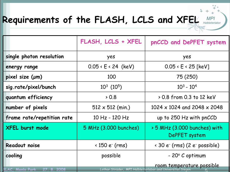
SLAC, Menlo Park 27. 8. 2008 Lothar Strüder, MPI Halbleiterlabor and Universität Siegen 5
Requirements of the FLASH, LCLS and XFEL
FLASH, LCLS + XFEL pnCCD and DePFET system
single photon resolution yes yes
energy range 0.05 < E < 24 (keV) 0.05 < E < 25 [keV]
pixel size (µm) 100 75 (250)
sig.rate/pixel/bunch 103 (105) 103 - 104
quantum efficiency > 0.8 > 0.8 from 0.3 to 12 keV
number of pixels 512 x 512 (min.) 1024 x 1024 and 2048 x 2048
frame rate/repetition rate 10 Hz - 120 Hz up to 250 Hz with pnCCD
XFEL burst mode 5 MHz (3.000 bunches) > 5 MHz (3.000 bunches) with DePFET system
Readout noise < 150 e- (rms) < 30 e- (rms) (2 e- possible)
cooling possible - 20o C optimum
room temperature possible
vacuum compatibility yes yes
preprocessing no (yes) ? possible upon request

SLAC, Menlo Park 27. 8. 2008 Lothar Strüder, MPI Halbleiterlabor and Universität Siegen 6
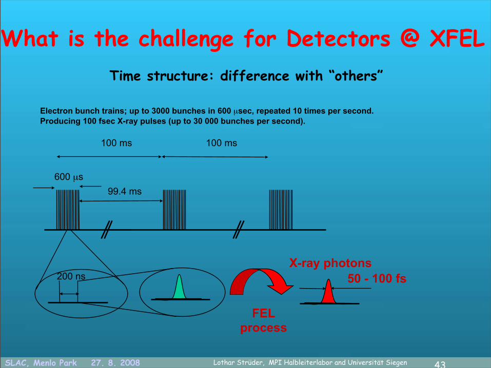
Time structure: difference with “others”
600 µs99.4 ms
100 ms 100 ms
200 ns
FELprocess
X-ray photons50 - 100 fs
Electron bunch trains; up to 3000 bunches in 600 µsec, repeated 10 times per second.Producing 100 fsec X-ray pulses (up to 30 000 bunches per second).
What is the challenge for Detectors @ XFEL ?

SLAC, Menlo Park 27. 8. 2008 Lothar Strüder, MPI Halbleiterlabor and Universität Siegen 6
Time structure: difference with “others”
600 µs99.4 ms
100 ms 100 ms
200 ns
FELprocess
X-ray photons50 - 100 fs
Electron bunch trains; up to 3000 bunches in 600 µsec, repeated 10 times per second.Producing 100 fsec X-ray pulses (up to 30 000 bunches per second).
What is the challenge for Detectors @ XFEL ?
30 000 bunches/sbut
99.4 ms (%) no photons

SLAC, Menlo Park 27. 8. 2008 Lothar Strüder, MPI Halbleiterlabor and Universität Siegen 7
What is limiting the quantum efficiency ?
The thickness of Silicon !!
Q.E. = 60 % @ 24 keVd = 2 mm
Q.E. = 22 % @ 24 keVd = 0.5 mm

SLAC, Menlo Park 27. 8. 2008 Lothar Strüder, MPI Halbleiterlabor and Universität Siegen 8
Thin entrancewindow
Silicon entrance windowwith x nm of SiO2
and y nm of Si3N4 plus
z nm of Al (optical shield)
optical light attenuation: 5 • 106
50 eV
Monolithic Integration of optical blocking filters
5 keV
SLAC, Menlo Park 27. 8. 2008 Lothar Strüder, MPI Halbleiterlabor and Universität Siegen 9
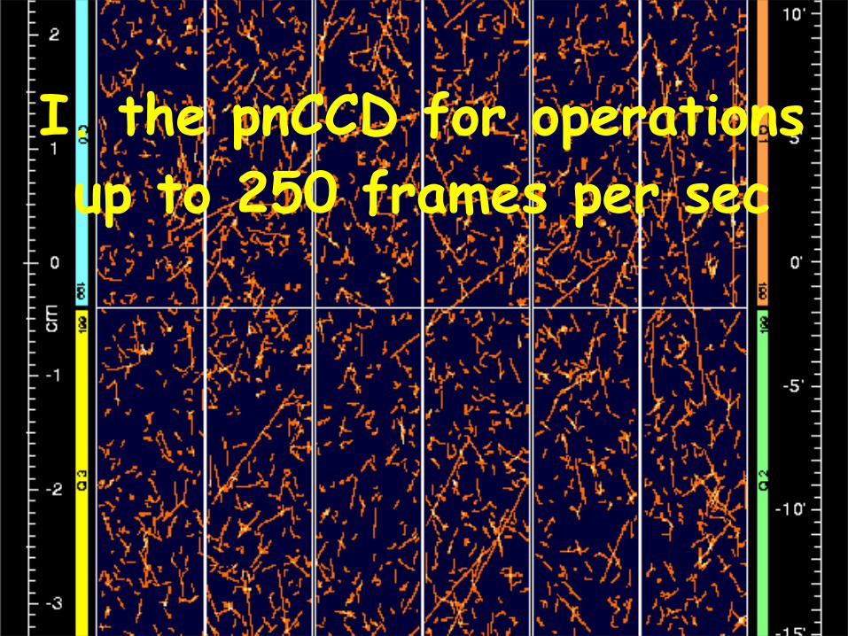
I. the pnCCD for operations up to 250 frames per sec

SLAC, Menlo Park 27. 8. 2008 Lothar Strüder, MPI Halbleiterlabor and Universität Siegen 9
II. the DePFET active pixel sensor for 200 ns frame acquisition time

SLAC, Menlo Park 27. 8. 2008 Lothar Strüder, MPI Halbleiterlabor and Universität Siegen 10
CCD basics
• full depletion (50 µm to 500 µm)• back side illumination• radiation hardness • high readout speed• pixel sizes from 36 µm to 650 µm• charge handling: more than 106 e-/pixel• high quantum efficiency

SLAC, Menlo Park 27. 8. 2008 Lothar Strüder, MPI Halbleiterlabor and Universität Siegen 11
How many charges can be stored
What determines the charge handling capacity in a pixel ?
pixel volume: 20x40x12 µm3 ≈ 1x104µm3
Doping: 102 P per µm3
CHC = 1 x 10⁶ per pixel
can be increased by external voltages
can be increased by doping

SLAC, Menlo Park 27. 8. 2008 Lothar Strüder, MPI Halbleiterlabor and Universität Siegen 12

SLAC, Menlo Park 27. 8. 2008 Lothar Strüder, MPI Halbleiterlabor and Universität Siegen 13
Hard X-ray SASE Free Electron Lasers
LINAC COHERENT LIGHT SOURCELCLS
SCSS SPring-8 Compact SASE Source
European XFEL Facility
2009
2010
2013
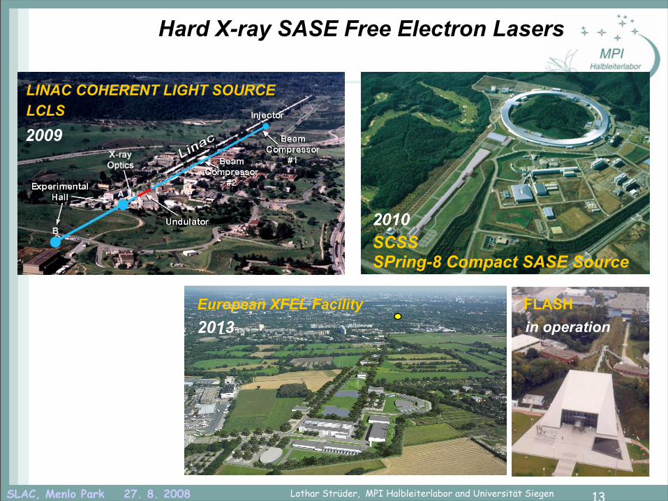
SLAC, Menlo Park 27. 8. 2008 Lothar Strüder, MPI Halbleiterlabor and Universität Siegen 13
Hard X-ray SASE Free Electron Lasers
LINAC COHERENT LIGHT SOURCELCLS
SCSS SPring-8 Compact SASE Source
European XFEL Facility
2009
2010
2013FLASHin operation

SLAC, Menlo Park 27. 8. 2008 Lothar Strüder, MPI Halbleiterlabor and Universität Siegen 13
Hard X-ray SASE Free Electron Lasers
LINAC COHERENT LIGHT SOURCELCLS
SCSS SPring-8 Compact SASE Source
European XFEL Facility
2009
2010
2013FLASHin operation
FLASH:the ice breaker for
XFELs

SLAC, Menlo Park 27. 8. 2008 Lothar Strüder, MPI Halbleiterlabor and Universität Siegen 13
Hard X-ray SASE Free Electron Lasers
LINAC COHERENT LIGHT SOURCELCLS
SCSS SPring-8 Compact SASE Source
European XFEL Facility
2009
2010
2013FLASHin operation
FLASH:the ice breaker for
XFELs
FLASH: 5 Hz, 10 Hz and 5 MHz
LCLS: 120 Hz
SCSS: 60 Hz
XFEL: 5 Hz, 10 Hz and 5 MHz

SLAC, Menlo Park 27. 8. 2008 Lothar Strüder, MPI Halbleiterlabor and Universität Siegen 14
Detectors for FLASH+LCLS+XFEL
insensitive gaps: ≈ 800 µm
Full Frame imagingarea per chip512 x 1024
pixel size75x75 µm2
Total sensitive system area:
59 cm
The full sensitive areaof the system is 59 cm2
with 75 µm pixels, 1024 x 1024
CMX
CMX
CMX
CMX
CMX
CMX
CMX
CMX
total areaper chip:29.5 cm2
readout time per frame: 4 ms i.e. 250 fps
can be triggered externally
device fabrication isfinished now
ADC
ADC
ADC
ADC
ADC
ADC
ADC
ADCADC
ADC
ADC
ADC
ADC
ADC
ADC
ADC ADC
ADC
ADC
ADC
ADC
ADC
ADC
ADC
ADC
ADC
ADC
ADC
ADC
ADC
ADC
ADC
16 ADCoutputs
16 ADCoutputs
hole diameter: 3 mm
transfer of signal charges
Chip 2: area 29.5 cm2
format: 1024 x 512
Chip 1: area 29.5 cm2
format: 1024 x 512

SLAC, Menlo Park 27. 8. 2008 Lothar Strüder, MPI Halbleiterlabor and Universität Siegen 15
pnCCD: 1024 x 512, 30 cm2
1024 p
ixel, 7.
8 cm
512 pixel, 3.7 cm
Area:
29.6 c
m2
for 6 keV X-rays the system delivers 4k x 4k resolution pointsin all the area with less than one photon per pixel (typ. 90 %)
Imaging 7.8 x 3.7 cm2 = 29.6 cm2
75 x 75 µm2
1024 parallel read nodes2 e- @ 250 fps

SLAC, Menlo Park 27. 8. 2008 Lothar Strüder, MPI Halbleiterlabor and Universität Siegen 16
Flex lead
Flex lead
Flex lead
Flex lead for - power - control - signal out - sequencing
ceramic carrier for thermal andstructural support
look at radiation entrancewindow side
CCD1
CCD2
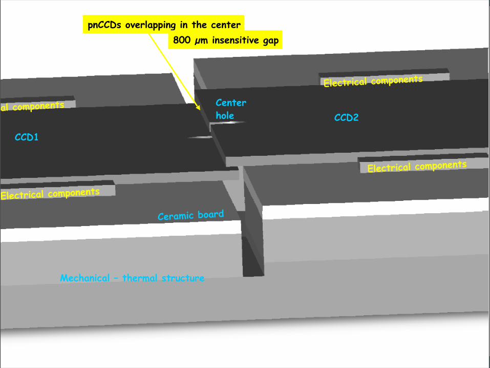
SLAC, Menlo Park 27. 8. 2008 Lothar Strüder, MPI Halbleiterlabor and Universität Siegen 17
CCD1
CCD2
Electrical components
Mechanical – thermal structure
Centerhole
Ceramic board
Electrical components
pnCCDs overlapping in the center
Electrical components
Electrical components
800 µm insensitive gap

SLAC, Menlo Park 27. 8. 2008 Lothar Strüder, MPI Halbleiterlabor and Universität Siegen 18
The CFEL-ASG Chamber
Reaction microscope: Many particle ion and electron imaging spectrometer Velocity map imagingAdditional feautures: Integration of jet-targets,ports for lasers, special injectors support structures for fixed targets, etc. . .

SLAC, Menlo Park 27. 8. 2008 Lothar Strüder, MPI Halbleiterlabor and Universität Siegen 19
The CFEL-ASG Chamber
Imaging system: For inside view the housing of C1 and C2 is drawn transparently. Detector 1 can have any position between Pmin with d(PIA;Pmin) = 5 cm
and Pmax with d(PIA;Pmax) = 300 mm. Detector 2 is mounted fixed at d(PIA;PD2) = 500 mm.

SLAC, Menlo Park 27. 8. 2008 Lothar Strüder, MPI Halbleiterlabor and Universität Siegen 20
The Imager of the CFEL-ASG Chamber
Imaging system: (a) format 1024x1024, pixel size 75x75 µm2, 8x8 cm2 focal surface
(b) center hole, typically 3 mm
Due to overlap of the two detectors, effective insensitive
area can be reduced to 1.6 mm, insensitive gaps: 0.8 mm
(c) movement in y-direction: up to 45 mm

SLAC, Menlo Park 27. 8. 2008 Lothar Strüder, MPI Halbleiterlabor and Universität Siegen 21
The Imager of the CFEL-ASG Chamber
System alignment: Detector 1 is movable in Y, Z and X (limited), 400 mm Ø Detector 2 is fixed, 250 mm Ø

SLAC, Menlo Park 27. 8. 2008 Lothar Strüder, MPI Halbleiterlabor and Universität Siegen 22
Detectors for FLASH+XFEL+PETRA III
Full Frame imaging,format per chip1024 x 1024
pixel size75x75 µm2
The full sensitive areaof the system is 239 cm2
with 75 µm pixels, 2048 x 2048
CMX
CMX
CMX
CMX
total area per chip:59 cm2, per system:
236 cm2
readout time per frame: ≈ 8 ms
i.e.≈ 125 fps
devices are scheduledfor fabrication end 2009ready: end 2010
ADC
ADC
ADC
ADC
ADC
ADC
ADC
ADCADC
ADC
ADC
ADC
ADC
ADC
ADC
ADC
16 ADCoutputs
Chip 1: area 59 cm2
format: 1024 x 1024
transfer of charges
This system is 3 – sidebuttable, can be extended toa 2048 x 2048 array
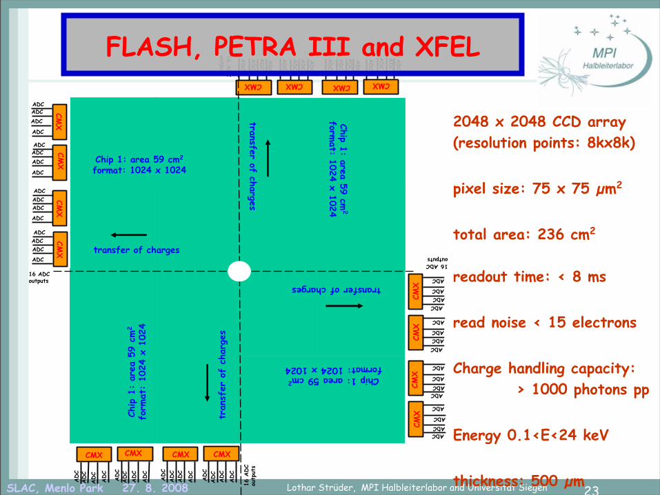
SLAC, Menlo Park 27. 8. 2008 Lothar Strüder, MPI Halbleiterlabor and Universität Siegen 23
2048 x 2048 CCD array(resolution points: 8kx8k)
pixel size: 75 x 75 µm2
total area: 236 cm2
readout time: < 8 ms
read noise < 15 electrons
Charge handling capacity: > 1000 photons pp
Energy 0.1<E<24 keV
thickness: 500 µm
operation temperature:-10oC
FLASH, PETRA III and XFEL

SLAC, Menlo Park 27. 8. 2008 Lothar Strüder, MPI Halbleiterlabor and Universität Siegen 24
Recent pnCCDs fabrications
prototype eROSITA version format: 256 x 256 x 2 pixel area: 3.7 cm2 + 2.5 cm2 pixel size: 75 x 75 µm2
flight type eROSITA versionformat: 384 x 384 x 2 pixel area: 8.4 cm2 + 5.6 cm2 pixel size: 75 x 75 µm2

SLAC, Menlo Park 27. 8. 2008 Lothar Strüder, MPI Halbleiterlabor and Universität Siegen 25
256 parallel low noise
readout channels with
2 or 4 output nodes
Frame store area
256 x 256 pixel
Imaging area256 x 256 pixel
Measurements with512x256 pnCCDs
@ FLASH + BESSY

SLAC, Menlo Park 27. 8. 2008 Lothar Strüder, MPI Halbleiterlabor and Universität Siegen 26
CAMEX block diagram
CD
S- fi
lter
JFET
- am
plifi
er
sam
ple
& h
old
cabl
e dr
iver
digital control
communication
seria
lizer
curr
ent s
ourc
e
IN
Vbst
Vsss
Sin
Stst
G1
G2
Sr1 S1 ... S8
Ss&hSmux
BW1 BW2
BW3
G4
Sr1
G3
pass
ive
low
pass
filte
r
Tst
OUT-
OUT+
Vdd
master reference DAC(s)Vref

SLAC, Menlo Park 27. 8. 2008 Lothar Strüder, MPI Halbleiterlabor and Universität Siegen 27
CAMEX eROSITA 128I-JD
CMX internal SEQ(shiftregister 16x64)
configurationregisters
differentialoutput buffer BIAS DACs BIAS master
reference
9153 um
6080
um
128 xcurrent source
128 xAMP &CDS-filter
S&HMUX

SLAC, Menlo Park 27. 8. 2008 Lothar Strüder, MPI Halbleiterlabor and Universität Siegen 2829
Development status: Flex lead + frontend PCB
- connects CCD module to front-end PCB by wedge bonds - front-end PCB: • analog output buffers (for the ADCs, one per CAMEX)• LVDS receivers • generators of the analog CCD clock pulses (PHI drivers) • connectors as electric interface to the camera electronics
DUO flex lead:→ performance testedeROSITA flex lead: → circuit diagram: under way→ layout: under way

SLAC, Menlo Park 27. 8. 2008 Lothar Strüder, MPI Halbleiterlabor and Universität Siegen 29
SLAC, Menlo Park 27. 8. 2008 Lothar Strüder, MPI Halbleiterlabor and Universität Siegen 30
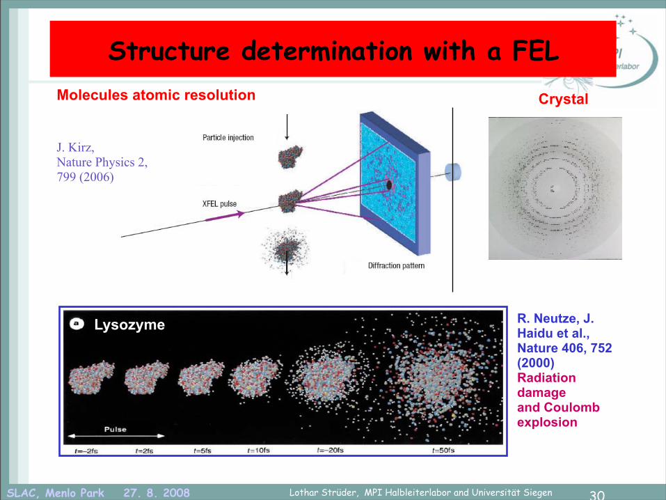
Molecules atomic resolution
Lysozyme R. Neutze, J. Haidu et al., Nature 406, 752 (2000)Radiation damageand Coulomb explosion
Structure determination with a FELCrystal
J. Kirz, Nature Physics 2, 799 (2006)

SLAC, Menlo Park 27. 8. 2008 Lothar Strüder, MPI Halbleiterlabor and Universität Siegen 31
Clusters “in the Flight”
FEL beam
MCP detector +phosphor screenskimmer
nozzle
CCD camera
beam dump
550 nm visible light
plane mirror
aperture
VUVscattered light
skimmer
cluster beam
aperture
Xe clusters CFEL Detectors
SLAC, Menlo Park 27. 8. 2008 Lothar Strüder, MPI Halbleiterlabor and Universität Siegen 32
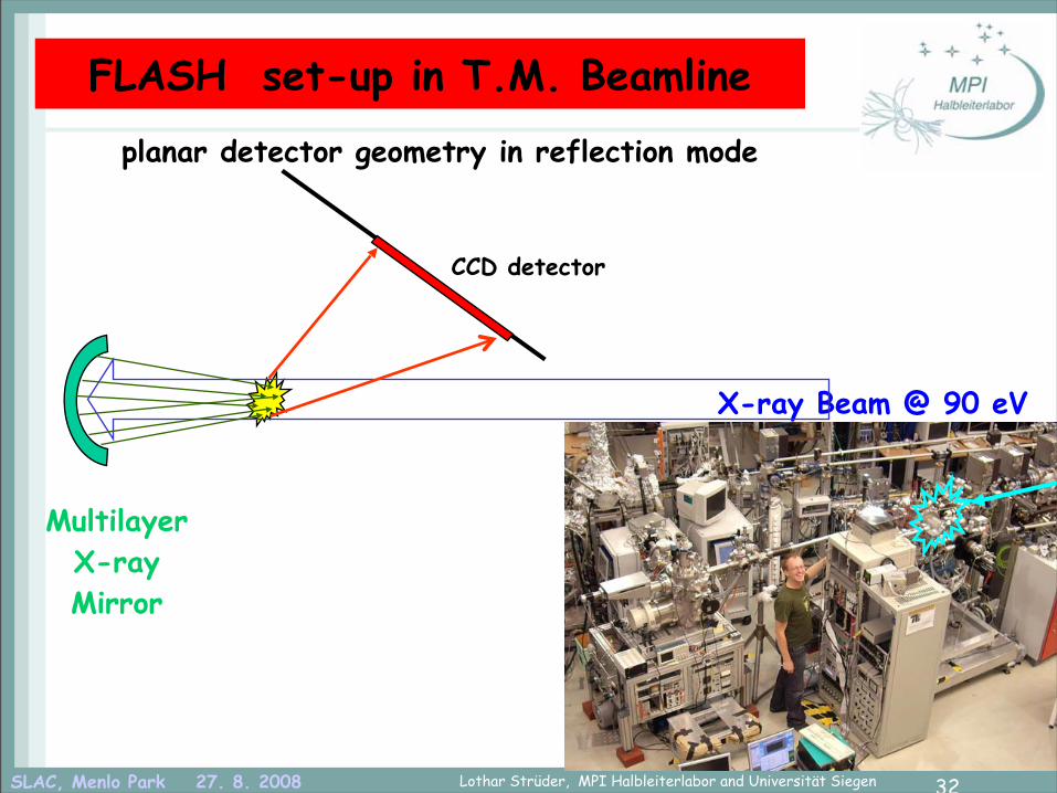
FLASH set-up in T.M. Beamline
planar detector geometry in reflection mode
X-ray Beam @ 90 eV
CCD detector
MultilayerX-rayMirror

SLAC, Menlo Park 27. 8. 2008 Lothar Strüder, MPI Halbleiterlabor and Universität Siegen 33
First observation of 32 nm Xe – nanocluster
simulation of 90 eV X-raysscattering at single Xenanoclusters with 32 nm size(C. Bostedt et al.)
field of view of the pnCCD during the experiment atthe FLASH X-ray free electronlaser facility at DESY, Hamburg

SLAC, Menlo Park 27. 8. 2008 Lothar Strüder, MPI Halbleiterlabor and Universität Siegen 34
90 eV X-rays in single photon counting mode !!!
FWHM: 38.9 eV
Spectrum from 4.000 frames with 0.05 photons/pixel/frame
T = -50° C
E = 90 eV➩25 ± 1.7 e-h pairsENC = 2.5 e- (rms)
trigger
threshold
30 eV

SLAC, Menlo Park 27. 8. 2008 Lothar Strüder, MPI Halbleiterlabor and Universität Siegen 35
Set-up in T.M. Beamline @ FLASH
pnCCD110o – 25o
pnCCD342o – 80o
pnCCD220o – 40o

SLAC, Menlo Park 27. 8. 2008 Lothar Strüder, MPI Halbleiterlabor and Universität Siegen 36
Clusters “in the Flight”
Collaboration: TU Berlin, MPI-HLL, MPI-K: Bostedt, Rupp, Adolph, Möller, Hartmann, Strüder, Rudenko, et al.

SLAC, Menlo Park 27. 8. 2008 Lothar Strüder, MPI Halbleiterlabor and Universität Siegen 37
Screen-Shots: To be evaluated!
Free Electron Lasers

SLAC, Menlo Park 27. 8. 2008 Lothar Strüder, MPI Halbleiterlabor and Universität Siegen 37
Screen-Shots: To be evaluated!
Free Electron Lasers

SLAC, Menlo Park 27. 8. 2008 Lothar Strüder, MPI Halbleiterlabor and Universität Siegen 38
Clusters “in the Flight”
Collaboration: TU Berlin, MPI-HLL, MPI-K: Bostedt, Rupp, Adolph, Möller, Hartmann, Strüder, Rudenko, et al.

SLAC, Menlo Park 27. 8. 2008 Lothar Strüder, MPI Halbleiterlabor and Universität Siegen 38
Clusters “in the Flight”
angle / deg
inte
nsity
/ pho
tons
per
pixe
l

SLAC, Menlo Park 27. 8. 2008 Lothar Strüder, MPI Halbleiterlabor and Universität Siegen 38
Clusters “in the Flight”
angle / deg
inte
nsity
/ pho
tons
per
pixe
l

SLAC, Menlo Park 27. 8. 2008 Lothar Strüder, MPI Halbleiterlabor and Universität Siegen 38
Clusters “in the Flight”
detector 1
detector 2 detector 3
angle / deg
inte
nsity
/ pho
tons
per
pixe
l

SLAC, Menlo Park 27. 8. 2008 Lothar Strüder, MPI Halbleiterlabor and Universität Siegen 38
Clusters “in the Flight”
detector 1
R = 83 nm
detector 2 detector 3
angle / deg
inte
nsity
/ pho
tons
per
pixe
l

SLAC, Menlo Park 27. 8. 2008 Lothar Strüder, MPI Halbleiterlabor and Universität Siegen 38
Clusters “in the Flight”
detector 1
R = 83 nm R = 80 nm
detector 2 detector 3
angle / deg
inte
nsity
/ pho
tons
per
pixe
l

SLAC, Menlo Park 27. 8. 2008 Lothar Strüder, MPI Halbleiterlabor and Universität Siegen 38
Clusters “in the Flight”
detector 1
R = 83 nm R = 80 nmWith strongly increased absorption!
detector 2 detector 3
angle / deg
inte
nsity
/ pho
tons
per
pixe
l Structure and Dynamics!

SLAC, Menlo Park 27. 8. 2008 Lothar Strüder, MPI Halbleiterlabor and Universität Siegen 39
In energy space: E = hc/(2*D*sin α)
E ≈ 6.2/(α*D)Peak distance : E n+1 – En ≈1/D
Bragg´s law in energy space
In angular space: λ=2 D sin α Peak distance : sinα n+1 – sinαn ≈ 1/DChanging footprint area
SLAC, Menlo Park 27. 8. 2008 Lothar Strüder, MPI Halbleiterlabor and Universität Siegen 40
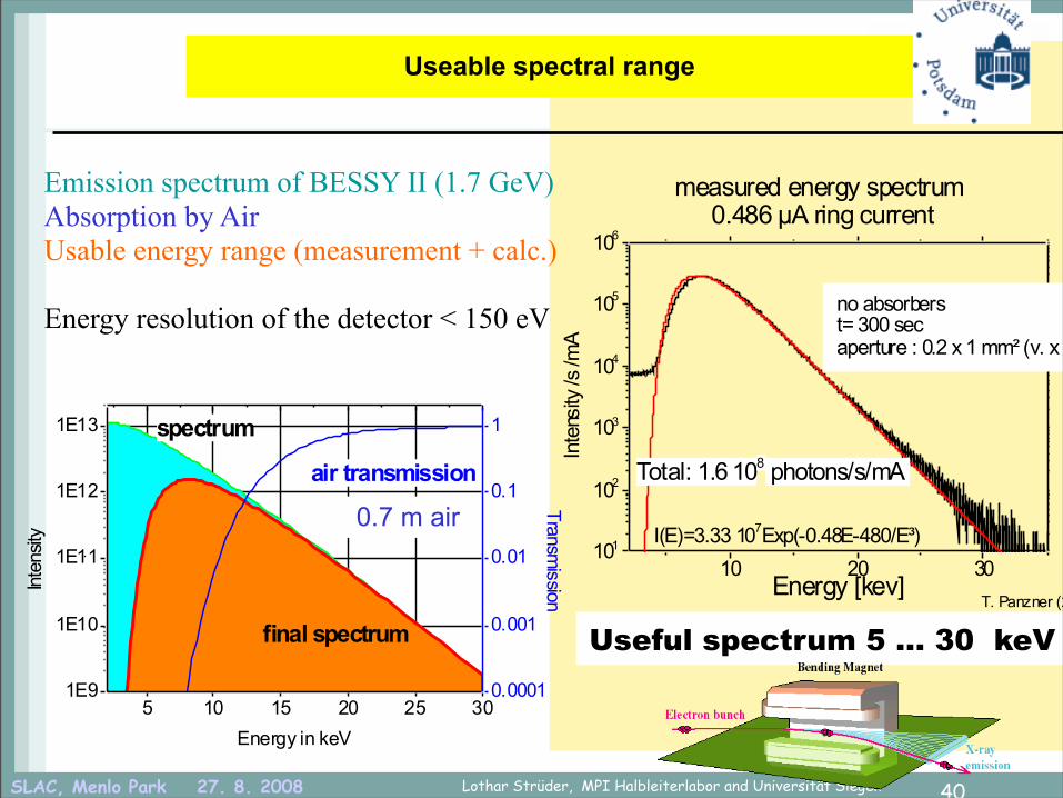
Useable spectral range
Emission spectrum of BESSY II (1.7 GeV)Absorption by Air Usable energy range (measurement + calc.)
Energy resolution of the detector < 150 eV
Useful spectrum 5 ... 30 keV
0.7 m air

SLAC, Menlo Park 27. 8. 2008 Lothar Strüder, MPI Halbleiterlabor and Universität Siegen 41
Langmuir-Blodgett-Filmfixed angle of incidenceFew minutes counting
1.000 to 10.000 photons per frame
400 to 1.000 frames per second
typical measurement times: 100 s to 1.000 s
position,time and energy resolvedphotons per spectrum: typ 108
αi = 0.8 deg

SLAC, Menlo Park 27. 8. 2008 Lothar Strüder, MPI Halbleiterlabor and Universität Siegen 42
pnCCD operating parameters
Parameter Frame Store pnCCD XMM type pnCCDpixel size 36 µm, 48 µm, 51 µm and 75 µm 150 µm
format 2562x2, 2642x2, 3842x2, 512x1024 64x200, 400x400
active area (image only) 3.9 cm2, 1.9 cm2, 8.3 cm2, 29 cm2 3 cm2, 36 cm2
sensitive depth 450 µm 300 µm
readout noise 2 – 2.5 electrons (rms) 5 electrons (rms)
Q.E. ≥ 90 % from 0.4 to 11 keV ≥ 90 % from 0.4 to 10 keV
charge handling ≥ 5 x 10⁵ electrons per pixel ≥ 5 x 10⁵ e per pixel
CTI @ 6 keV 1 x 10⁻⁵ 50 x 10-5
Δ E 40 eV @ 300 eV, 125 eV @ 6 keV -- , 150 eV @ 6 keV
readout time 10 µs or 20 µs per row 25 µs per row
pixel rate 13 Mpix or 25 Mpix per second 2.8 Mpix per second
frame rate up to 900 fps, 20 fps for eROSITA 14 fps
out-of –time events 0.2 % in the case of eROSITA 6%
power dissipation in FP eROSITA: 0.5 W per 9 cm2 0.7 W for 36 cm2
power dissipation per pix. eROSITA: 0.2 µJ per pixel readout 0.33 µJ per pixel readout
SLAC, Menlo Park 27. 8. 2008 Lothar Strüder, MPI Halbleiterlabor and Universität Siegen 43
Time structure: difference with “others”
600 µs99.4 ms
100 ms 100 ms
200 ns
FELprocess
X-ray photons50 - 100 fs
Electron bunch trains; up to 3000 bunches in 600 µsec, repeated 10 times per second.Producing 100 fsec X-ray pulses (up to 30 000 bunches per second).
What is the challenge for Detectors @ XFEL ?

SLAC, Menlo Park 27. 8. 2008 Lothar Strüder, MPI Halbleiterlabor and Universität Siegen 44
Vdrift ≈ 13 µm/ns (i.e. ~3.5V/30µm bias) Tdrift, max = 1000 ns
1.28 cm(64 pixels)
on-chip electr.
on-chip electr.
128 channels
128 channels
1.28 cm(64 pixels)
1 MHz frame
200µm pixel
E=2-20 keV
103 X-rays
QE>80%@10keV
ENC~50 el.
Expandable to:
512x512 (monolithic)
1000 ns
1000 ns (Δx=200µm,Δt=15 ns)
Original LSDD Concept: reduce number of readout channels by time multiplexing
Limitations of that concept: frame rate limited to 1 MHz limited dynamic range, limited occupancy system noise difficult to achieve @ 5 ns shaping

SLAC, Menlo Park 27. 8. 2008 Lothar Strüder, MPI Halbleiterlabor and Universität Siegen 45
esa´s, NASA‘sand JAXA‘sIXO missionin 2021
SLAC, Menlo Park 27. 8. 2008 Lothar Strüder, MPI Halbleiterlabor and Universität Siegen 46
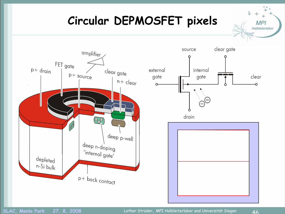
Circular DEPMOSFET pixels

SLAC, Menlo Park 27. 8. 2008 Lothar Strüder, MPI Halbleiterlabor and Universität Siegen 46
Circular DEPMOSFET pixels

SLAC, Menlo Park 27. 8. 2008 Lothar Strüder, MPI Halbleiterlabor and Universität Siegen 47
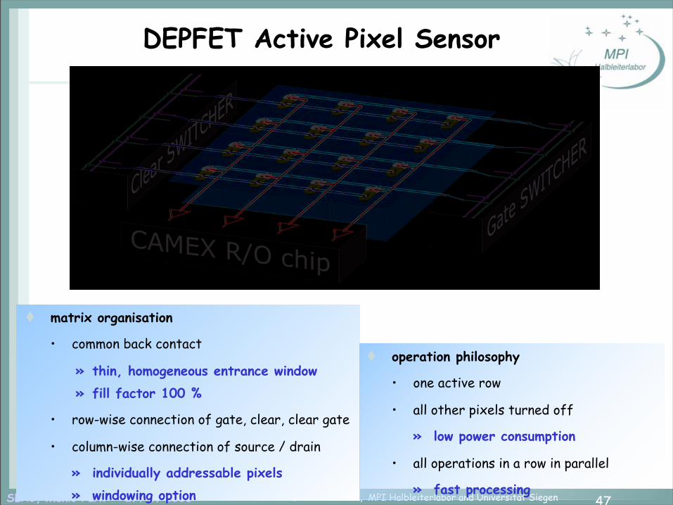
matrix organisation
• common back contact
» thin, homogeneous entrance window » fill factor 100 %
• row-wise connection of gate, clear, clear gate
• column-wise connection of source / drain
» individually addressable pixels » windowing option
DEPFET Active Pixel Sensor
operation philosophy
• one active row
• all other pixels turned off
» low power consumption
• all operations in a row in parallel
» fast processing

SLAC, Menlo Park 27. 8. 2008 Lothar Strüder, MPI Halbleiterlabor and Universität Siegen 47
matrix organisation
• common back contact
» thin, homogeneous entrance window » fill factor 100 %
• row-wise connection of gate, clear, clear gate
• column-wise connection of source / drain
» individually addressable pixels » windowing option
DEPFET Active Pixel Sensor
operation philosophy
• one active row
• all other pixels turned off
» low power consumption
• all operations in a row in parallel
» fast processing

SLAC, Menlo Park 27. 8. 2008 Lothar Strüder, MPI Halbleiterlabor and Universität Siegen 48
SIMBOL-X-Hybrid
3.2 cm
3.2 cm
SLAC, Menlo Park 27. 8. 2008 Lothar Strüder, MPI Halbleiterlabor and Universität Siegen 49
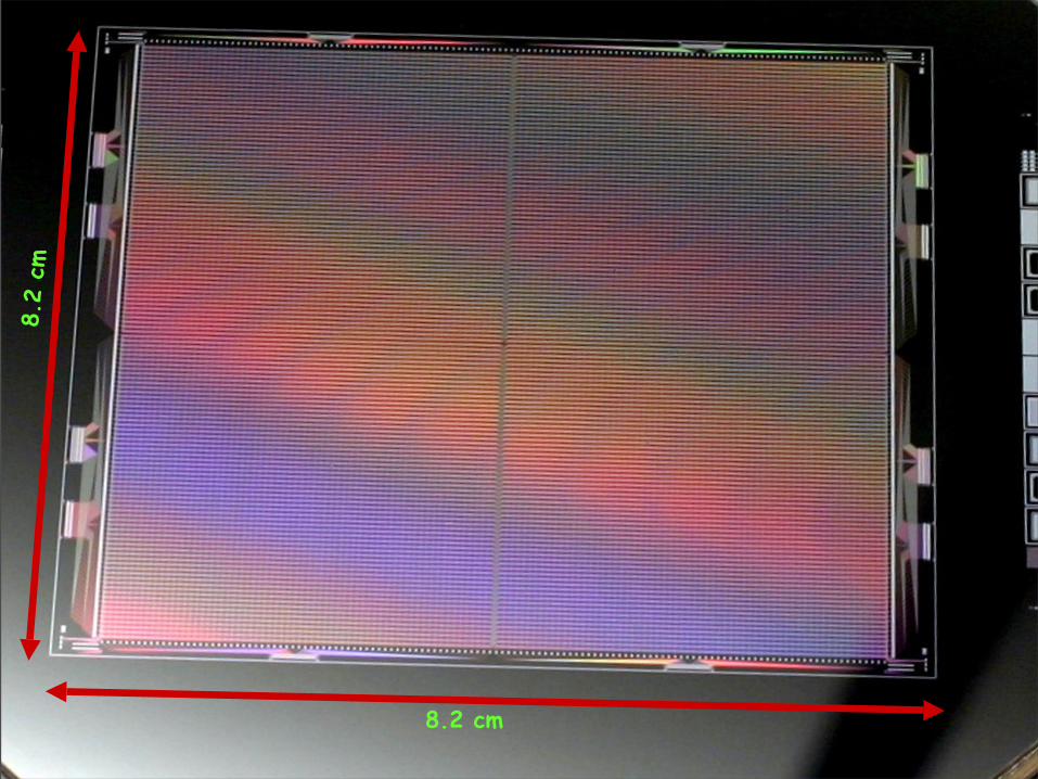
8.2 cm
8.2
cm

SLAC, Menlo Park 27. 8. 2008 Lothar Strüder, MPI Halbleiterlabor and Universität Siegen 50
DePMOS Active PixelSensor
Connecting Bumps• 1 per pixel
CMOS Layer• Signal processing• Signal storage & output
X-rays
Hybrid Pixel Detector Approach

SLAC, Menlo Park 27. 8. 2008 Lothar Strüder, MPI Halbleiterlabor and Universität Siegen 51
DePFET system overview

SLAC, Menlo Park 27. 8. 2008 Lothar Strüder, MPI Halbleiterlabor and Universität Siegen 52
Basic concept
Internal gate extends below large area source
Small signal charge is collected below transistor channel
Large signal charges distributed also over outer regions of internal gate; only the fraction below channel steers the transistor current efficiently
This arrangement leads to a non linear characteristics
The shape of this characteristics can be tuned by the doping profile of the internal gate
Clearing electrode is not shown in the picture

SLAC, Menlo Park 27. 8. 2008 Lothar Strüder, MPI Halbleiterlabor and Universität Siegen 53
pixel size: 200x200 µm2
can be realized from 75 x 75 µm2 to300 x 300 µm2
5 deep n implants for the graded internal gate
clear
source
drain
gate
drift ring

SLAC, Menlo Park 27. 8. 2008 Lothar Strüder, MPI Halbleiterlabor and Universität Siegen 54
Non-linear DEPFET: Simulation
37 consecutive steps of
10-14 C charge deposition were simulated: i.e.
37 x 62.500 e- = 2.312.500 e-
Resulting drain current
Δ I = 130 µA
and

SLAC, Menlo Park 27. 8. 2008 Lothar Strüder, MPI Halbleiterlabor and Universität Siegen 55
DePFET output characteristics
this corresponds to 40 × 6.25 x 104 e- = 2.5 x 10⁶ e-
i.e. 1.000 photons of 10 keV per pixel

SLAC, Menlo Park 27. 8. 2008 Lothar Strüder, MPI Halbleiterlabor and Universität Siegen 56
Timing behaviour of the DePFET

SLAC, Menlo Park 27. 8. 2008 Lothar Strüder, MPI Halbleiterlabor and Universität Siegen 57
Radiation damage tests
Generation and saturation of surface states

SLAC, Menlo Park 27. 8. 2008 Lothar Strüder, MPI Halbleiterlabor and Universität Siegen 58
Surface charge generation

SLAC, Menlo Park 27. 8. 2008 Lothar Strüder, MPI Halbleiterlabor and Universität Siegen 59
Charge cloud expansion
Plasma effects are not included
Deformation of the local electric field is not included

SLAC, Menlo Park 27. 8. 2008 Lothar Strüder, MPI Halbleiterlabor and Universität Siegen 60
potential
electronconcentrationafter50 ps
electronconcentrationafter1.3 ns
electron dynamics
injection of400.000 electrons
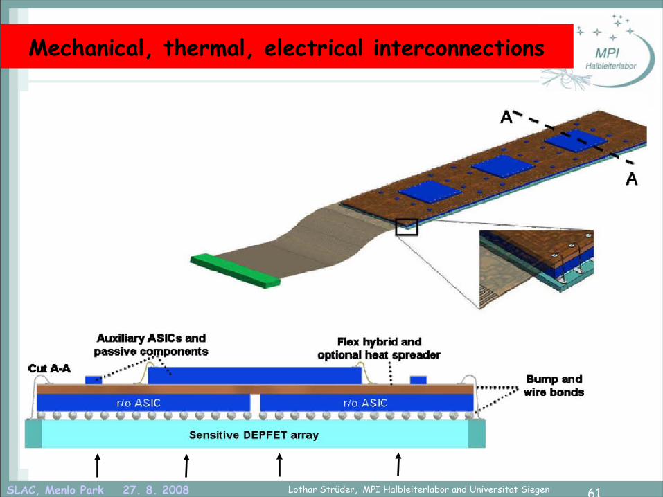
SLAC, Menlo Park 27. 8. 2008 Lothar Strüder, MPI Halbleiterlabor and Universität Siegen 61
Mechanical, thermal, electrical interconnections

SLAC, Menlo Park 27. 8. 2008 Lothar Strüder, MPI Halbleiterlabor and Universität Siegen 62
What is achieved (by simulation) up to now:
high dynamic range from single photon counting @ 1 keV up to 1.000 photons @ 10 keV in one single pixel
the maximum voltage swing at the on-chip amplifier never exceeds 1 V
highest resolution @ low signals, lowest resolution
@ the highest photon densities. Intensity resolution
is matched with the precision of the Poisson statistics
of the incoming photons
the charge collection, the signal processing and the charge

SLAC, Menlo Park 27. 8. 2008 Lothar Strüder, MPI Halbleiterlabor and Universität Siegen 63
Development system philosophy
prototype systemwith64 x 64 or128 x 128pixel
breadboard system with512 x 128pixel
full quadrant system with at least512 x 512 pixel

SLAC, Menlo Park 27. 8. 2008 Lothar Strüder, MPI Halbleiterlabor and Universität Siegen 64
Full DePFET system (1k x 1k)
one quadrant, composedby 4 ladders
fill factor: ≈ 90 %
a qualified prototypeshould be availablein 3 years
the breadboard systemin 4.5 years
and the full system in6 years from now

SLAC, Menlo Park 27. 8. 2008 Lothar Strüder, MPI Halbleiterlabor and Universität Siegen 65
Conclusions:1. the proposed DePFET detector covers • the dynamic range • the required noise performance • pixel size • area fill factor • charge collection, signal filtering and reset are within 200 ns
2. the anticipated pixel area of 200 x 200 µm2
allows for the integration of a pixelwise analog signal processing, digitization and data storage with a 130 nm process
3. radiation hardness for X-rays seem to be sufficient
4. mounting, interconnection and cooling can be realized with "conventional" techniques

SLAC, Menlo Park 27. 8. 2008 Lothar Strüder, MPI Halbleiterlabor and Universität Siegen 66
Conclusions
Phase I + II ❒ fast pnCCD systems will cover the parameter space for FLASH, LCLS, SCSS and XFEL
except for the 5 MHz operation Phase III ❒ DePFET type active pixel sensors will cover the ultrafast imaging modes up to 5 MHz frame rates in 2014
Both systems are: highly efficient, high speed, low noise and radiation hard