design of operational transconductance amplifier with ... papers/midem_47(2017)3p187.pdf187 original...
TRANSCRIPT
187
Original scientific paper
MIDEM Society
1 Introduction
In the paper, an integrated circuit including a symmet-rical Operational Transconductance Amplifier (OTA) with temperature compensation is described. The OTA can be presented as a voltage controlled current source. The ideal OTA has very high input and output impedances and a wide frequency bandwidth. The out-put current IOUT is proportional to the differential input voltage and is expressed as:
dmOUT VgI = (1)
where gm is the transconductance of the amplifier and Vd is the differential input voltage.
Design of Operational Transconductance Amplifier with Temperature CompensationDamjan Berčan, Aleksander Sešek, Janez Trontelj
University of Ljubljana, Faculty of Electrical Engineering, Laboratory for Microelectronics
Abstract: In this paper an operational transconductance amplifier [1] with temperature compensation is presented. It is a voltage-controlled current source, which operates in an open loop configuration with a single output connected to a resistive load. The amplifier is internally compensated to keep the gain stable over the -40 °C to 125 °C temperature range. It features low input voltage noise and operates at supply voltages from 3 V to 5.5 V. Additionally, an internal 1.21 V bandgap reference is used to ensure a stable internal voltage reference point. The active area of the proposed integrated circuit designed with 0.18 µm Bipolar, CMOS, DMOS (BCD) technology is 750 µm x 260 µm. It consumes 423 µA of current and it has 8.87 nV/SHz of input noise at 500 kHz. The resulting simulated voltage gain is 40 dB and variations are less than ±0.3 dB over the temperature range of -40 °C to 125 °C.
Keywords: Operational Transconductance Amplifier; Temperature compensated bias current; Temperature sensitivity optimization
Načrtovanje operacijskega transkonduktančnega ojačevalnika s temperaturno kompenzacijoIzvleček: V članku je predstavljen transkonduktančni ojačevalnik s temperaturno kompenzacijo. Na izhod odprto-zančnega ojačevalnika oziroma napetostno krmiljenega tokovnega vira je priključeno uporovno breme. Notranja kompenzacija skrbi za stabilno ojačenje v temperaturnem območju od -40 °C do 125 °C. Poleg tega ojačevalnik izkazuje majhen vhodni šum in deluje v napetostnem območju od 3 V do 5.5 V. Vezje vsebuje napetostno referenco, ki poskrbi za stabilno referenčno točko. Integrirano vezje je bilo načrtano v 0.18 µm BCD (Bipolar, CMOS, DMOS) tehnologiji, njegova aktivna površina znaša 750 µm x 260 µm. Poraba ojačevalnika znaša 423 µA, njegova šumna gostota na vhodu je 8.87 nV/SHz pri frekvenci 500 kHz. Napetostno ojačenje znaša 40 dB in v temperaturnem območju od -40 °C do 125 °C odstopa za manj kot ±0.3 dB.
Ključne besede: Transkonduktančni operacijski ojačevalnik; temperaturna kompenzacija delovnega toka; optimizacija temperaturne občutljivosti
* Corresponding Author’s e-mail: [email protected]
Journal of Microelectronics, Electronic Components and MaterialsVol. 47, No. 3(2017), 187 – 192
One of the major drawbacks of the OTA is its high tem-perature sensitivity, caused by inversely proportional temperature variations of gm [2, 3]. Transconductance of the Metal-Oxide-Semiconductor (MOS) transistor, using small signal model in saturation region is defined as follows:
Doxnm I
LWCg )(2µ= (2)
where µn is carrier mobility, Cox is oxide capacitance, W is width of the device, L is length of the channel and ID is drain current [4].

188
The root cause of temperature variations is the temper-ature dependent threshold voltage VT and the carrier mobility µn variations of the MOS transistor, according to equations (2) and (3):
)()()( 00 TTTVTV VTTT −+= α (3)
µα
µµ
=
00 )()(TTTT nn (4)
where T0 is the reference temperature (300 °K), αVT and αµ are negative values which vary with temperature [5]. As one of possible solutions, a circuit with output voltage Proportional To Absolute Temperature (PTAT) can be implemented to compensate the temperature variations of gm. The difference between the two base-emitter voltages in PTAT is expressed as:
)/ln( 12 JJVV tBE =∆ (5)
where Vt is thermal voltage and J1, J2 are different cur-rent densities of bipolar transistors. The PTAT circuit generates voltage which has a positive Temperature Coefficient (TC) [4].
The following section (Section 2) presents the OTA design method to overcome the mentioned problem. In section 3, simulation results for typical simulation conditions, pro-cess variations and Monte Carlo analyses are presented.
2 Ota circuit design
The block diagram of the OTA with temperature com-pensation is shown in Fig.1. The main advantage of the proposed solution is the temperature compensated bias current. The compensation circuit consists of two resistors (R1 and R2) having different TC. The block dia-gram also includes internal a 1.21 V voltage reference (Vref), biasing current generator (Ibias generator) which compensate the temperature variations of gm, two Op-erational Amplifiers (OPA1 and OPA2) for voltage to current conversion and OTA circuit. Our objective was to keep the gain of the OTA stable over the -40 °C to
Figure 1: Block diagram of integrated circuit.
Figure 2: The schematic of integrated circuit.
D. Berčan et al; Informacije Midem, Vol. 47, No. 3(2017), 187 – 192

189
125 °C temperature range, low input voltage noise and high Power Supply Rejection Ratio (PSRR).
2.1 Topology of the circuit
The schematic of the balanced OTA with temperature compensation is shown in the Fig. 2. The voltage to currents converters are used to convert the reference bandgap voltage to the corresponding current. Both converters are designed as classic two stage amplifi-ers with a N type Metal-Oxide-Semiconductor (NMOS) input differential stage and a common source output stage including compensation capacitor and resistor. To ensure precise conversion, the temperature stable reference voltage is employed. The voltage reference - bandgap circuit, maintains a stable voltage over the temperature range and power supply voltage varia-tions. The OTA consists of NMOS input differential stage and three current mirrors. Transistors M20 – M23 form the first current mirror stage, M25 – M28 form the sec-ond current mirror stage and M13, M14, M18 and M19 form the third current mirror stage. To increase the out-put impedance the cascode current mirrors are used. The gate of transistors are connected and biased as low voltage cascode, which keeps the minimum drain source voltages of transistor M13, M22 and M25 and also insures transistor saturation operation. The Length (L) of transistor M10 is higher in order to compensate the body effect of cascode transistors M14 and M18 [6].
2.4 Compensation circuit
The compensation circuit consists of transistors M9 and M10 and two resistors (R1 and R2) with different TC, which is calculated using the box-method [7], -1618 ppm/ᵒC and 1322 ppm/ᵒC, respectively. The Fig. 3 pres-ents the currents IR1 and IR2, determined by resistors R1 and R2, and bias current Ibias, flowing through M10.
The compensation circuit generates bias current Ibias which is stated as:
Figure 3: Generated currents.
21 RRbias III +−= (6)
The bias current Ibias increases with temperature com-pensating decreasing transconductance of OTA.
3 Simulation results
3.2 Results for typical simulation parameters
The typical process parameters simulations at 25 °C were performed for the supply voltages 3.3 V and 5 V, respectively. The simulation results are presented in Table 1. Input noise density was measured at 500 kHz.
Table 1: Simulation results at typical simulation condi-tions.
Param. \ Suppl. 3.3 V 5 V Units
Ivdda 423 540 µA
G 40.2 40.4 dB
BW 13.6 15.0 MHz
Input noise density 8.87 8.56 nV/√Hz
Input offset voltage 1.08 1.99 mV
CMRR -132 -142 dB
+SR 9.01 9.60 V/µs
-SR 9.23 9.72 V/µs
PSRR @ 100 Hz -73.5 -78.2 dB
Transconductance 778 737 µA/V
The input referred noise voltage can be further reduced by changing the channel W/L ratio of the M15 and M16 transistors or increasing the bias current Ibias. This ac-tion would lead to larger chip area (higher cost) and higher power consumption. To reduce the offset which effects the performance of the OTA, the auto-zeroing or chopping technique method could be used, adding complexity to the design. Precise matching strategies of the transistors and resistors devices must be used to minimize offsets and provide symmetry.
Typical performance characteristics for a 3.3 V supply voltage are shown from Figures 4 to 7. The input re-ferred noise voltage was measured at 500 kHz, while PSRR was measured at 100 Hz.
Fig. 4 shows the voltage gain vs. frequency at three temperatures (-40 °C, 25 °C, 125°C), which is 40 dB. The results show that the gain sensitivity to temperature variations are almost eliminated with the presented design. The bandwidth of the OTA varies from 14.1 MHz at -40 °C to 12.8 MHz at 125 °C.
D. Berčan et al; Informacije Midem, Vol. 47, No. 3(2017), 187 – 192

190
Figure 4: Voltage Gain vs. Frequency
Fig. 5 presents input referred noise voltage density as a function of frequency at temperatures (-40 °C, 25 °C, 125°C). The noise measured at 500 kHz increases with temperature from 8.16 nV/√Hz at -40 °C to 10.1 nV/√Hz at 125 °C.
Figure 5: Input Noise Voltage vs. Frequency
The Common Mode Rejection Ratio (CMRR) is meas-ured as the ratio of the common mode gain to differ-
ential mode gain. At lower frequencies the CMRR varies from -131 dB at -40 °C to -121 dB at 125 °C. The results are shown in Fig. 6.
Figure 6: CMRR vs. Frequency
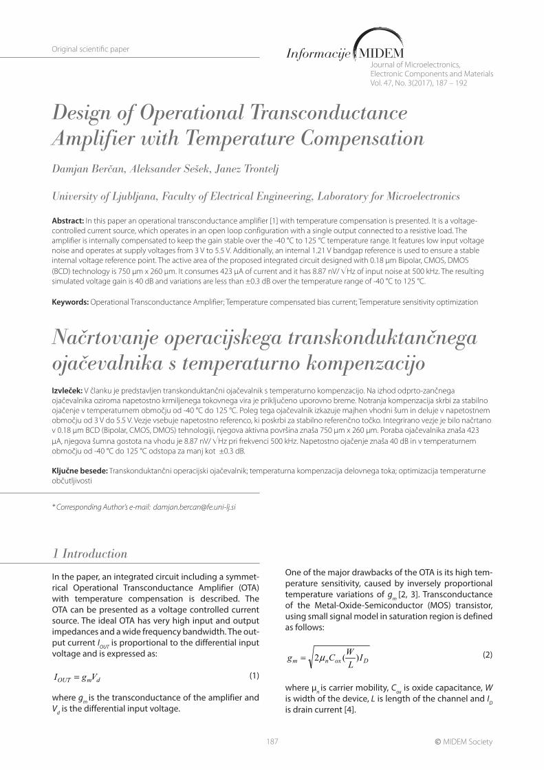
The PSRR is measured as the ratio of the OTA output variation vs. the supply voltage variation regardless the input signal. The PSRR varies from -78.2 dB at -40 °C to -62.9 dB at 125 °C, measured at 100 Hz. At higher fre-quencies, PSRR deteriorates. The results are shown in Fig. 7.
3.2.1 Corner analysis
The process variations of MOSFETs and resistors influ-ence on performance of fabricated integrated circuit. Therefore, the OTA was simulated for different process corners – four corner models (FF, SS, FS and SF). The re-sults at 25 °C are gathered in Table 2. The input noise density was measured at 500 kHz.
3.2.2 Monte Carlo simulation
In this section the results of the Monte Carlo (MC) anal-ysis are shown. The MC simulations were performed
Table 2: Corner analysis results
Parameters FF1 SS1 FS1 SF1 FF2 SS2 FS2 SF2 UnitsIvdda 485 374 430 416 621 476 550 530 µAG 41.3 39.2 40.2 40.1 41.5 39.4 40.45 40.32 dBBW 14.5 12.6 13.8 13.3 16.0 14.0 15.2 14.7 MHzInput noise density 8.25 9.43 8.81 8.92 7.95 9.13 8.50 8.62 nV/SHzOffset 1.57 0.71 1.16 1.00 2.72 1.37 2.11 1.89 mVCMRR -132 -130 -134 -129 -140 -144 -141 -143 dB+SR 10.28 8.02 9.06 8.95 10.97 8.54 9.66 9.54 V/µs-SR 10.54 8.19 9.3 9.13 11.1 8.65 9.79 9.66 V/µsPSRR @ 100 Hz -68.9 -78.5 -75.3 -72.1 -73.8 -83.5 -81.3 -75.8 dBTransconductance 856 715 785 770 816 672 737 737 µA/V
Note1: Supply voltage: 3.3 VNote2: Supply voltage: 5 V
D. Berčan et al; Informacije Midem, Vol. 47, No. 3(2017), 187 – 192
191
including mismatch and process variations at typical conditions (25 °C and 3.3 V) comprising 512 MC runs. The simulation results are presented in the following histograms.
Figure 7: PSRR vs. Frequency
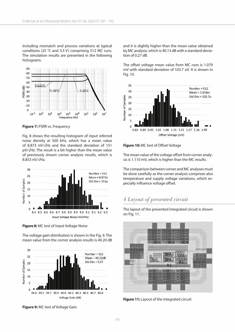
Fig. 8 shows the resulting histogram of input referred noise density at 500 kHz, which has a mean value of 8.873 nV/√Hz and the standard deviation of 151 pV/√Hz. The result is a bit higher than the mean value of previously shown corner analysis results, which is 8.853 nV/√Hz.
Figure 8: MC test of Input Voltage Noise
The voltage gain distribution is shown in the Fig. 9. The mean value from the corner analysis results is 40.20 dB
and it is slightly higher than the mean value obtained by MC analysis, which is 40.13 dB with a standard devia-tion of 0.27 dB.
The offset voltage mean value from MC runs is 1.079 mV with standard deviation of 103.7 uV. It is shown in Fig. 10.
Figure 10: MC test of Offset Voltage
The mean value of the voltage offset from corner analy-sis is 1.110 mV, which is higher than the MC results.
The comparison between corner and MC analyses must be done carefully as the corner analysis comprises also temperature and supply voltage variations, which es-pecially influence voltage offset.
4 Layout of presented circuit
The layout of the presented integrated circuit is shown on Fig. 11.
Figure 11: Layout of the integrated circuit
Figure 9: MC test of Voltage Gain
D. Berčan et al; Informacije Midem, Vol. 47, No. 3(2017), 187 – 192

192
The active area of the circuit, without bonding pads and supply connection rings, is 750 µm x 260 µm. The integrated circuit has been designed with the 0.18 µm BCD technology as a part of the System on Chip (SoC). The BCD technology allows mixed - signal design using low and high voltage transistors (DMOS) on the same die (reduces cost, area and power consumption). The voltage to current converter main part is presented by resistors R1 – N+ poly without salicide and R2 – N+ dif-fusion without salicide, which means that resistors do not have an additional process mask of salicide, reduc-ing the sheet resistance (Ω/sq) of the resistors. For ASIC area reduction, N – well resistors could be used, but they have high nonlinearity and larger parasitic capaci-tance between N – well and substrate. The integrated circuit has been sent to the fabrication factory.
5 Conclusions and next steps
The OTA was designed and analyzed using the 0.18 µm BCD technology. The temperature sensitivity of the OTA has been optimized and reduced, using the bias control technique and a stable internal voltage refer-ence. The proposed circuit shows voltage gain varia-tions lower than ±0.3 dB in the temperature range from -40 °C to 125 °C and lower than 0.5 dB when varying the supply voltage in the range from 3 V to 5.5 V. The equivalent input referred noise voltage is simulated to be lower than 10 nV/√Hz at 500 kHz and 25 °C, and volt-age offset lower than 2.8 mV. To overcome the problem of process variations, especially the resistors R1 and R2 which are used for compensation current generation and are one of the most critical elements in compen-sations circuit, the resistance of both R1 and R2 resis-tors will be precisely trimmed. The issue could be eas-ily solved by employing effective and uncomplicated trimming resistor stage for each of them separately and internal One-Time-Programmable (OTP) memory cells.
6 References
1. W. M. C. Sansen, Analog Design Essentials, let. 2006. Springer US.
2. W. Surakampontorn, V. Riewruja, K. Kumwachara, C. Surawatpunya, in K. Anuntahirunrat, „Tempera-ture-insensitive voltage-to-current converter and its applications“, IEEE Trans. Instrum. Meas., let. 48, št. 6, str. 1270–1277, dec. 1999.
3. T. Parveen, A textbook of operational transconduct-ance amplifier and analog integrated circuits. New Delhi: I. K. International Publishing House, 2012.
4. A. Pleteršek, Načrtovanje analognih integriranih vezij v tehnologijah CMOS in BiCMOS. Ljubljana: Fakulteta za elektrotehniko, 2006.
5. I. M. Filanovsky in A. Allam, „Mutual compensation of mobility and threshold voltage temperature effects with applications in CMOS circuits“, IEEE Trans. Circuits Syst. Fundam. Theory Appl., let. 48, št. 7, str. 876–884, jul. 2001.
6. T. C. Carusone, K. W. Martin, in D. Johns, Analog in-tegrated circuit design, 2nd edition. Hoboken, N.J.: John Wiley & Sons, 2011.
7. M. E. T. Instruments, „Voltage Reference Selection Basics“. Available at: http://www.ti.com/lit/wp/slpy003/slpy003.pdf. Accessed: [6.8.2016]
Arrived: 31. 08. 2017 Accepted: 11. 12. 2017
D. Berčan et al; Informacije Midem, Vol. 47, No. 3(2017), 187 – 192