design of an audio power amplifier with a notch in the output...
TRANSCRIPT

University of Twente
Faculty of Electrical Engineering, Mathematics & Computer Science
Design of an audio power amplifier with a notch in
the output impedance
Remco Twelkemeijer MSc. Thesis May 2008
Supervisors: prof. ir. A.J.M. van Tuijl
dr. ir. R.A.R. van der Zee ir. F. van Houwelingen
Report number: 067.3264
Chair of Integrated Circuit Design Faculty of Electrical Engineering, Mathematics & Computer Science
University of Twente P. O. Box 217
7500 AE Enschede


Abstract This report is about the research and design of an audio power amplifier with a notch in the output impedance. A notch in the output impedance could be beneficial if the amplifier is set in parallel with a class D amplifier. In this combination, the amplifier should remove the high frequency switching ripple of the class D amplifier. Investigation of the output impedance with a pole zero analysis determines the theoretical possibilities about a notch in the output impedance. A notch in the output impedance can be created by a peak filter in the amplifier. An amplifier containing a peak filter is designed with ideal components, like transconductances and inductors. Different filters are investigated to implement a peak filter in an IC process. These filters are created by ideal switches and capacitors. To evaluate their usability, simulations are done with amplifiers containing those filters in combination with a class D amplifier. The report shows that a notch can be created at the cost of some increase in the distortion. This can be compensated by increasing the power consumption of the amplifier. Also a small peak in the output impedance is introduced. The peak in the output impedance results in a ringing when a step response is applied. Simulations results in the conclusion that it seems not beneficial to use an amplifier with a notch in the output impedance, if the notch should remove the switching ripple of the class D amplifier.


Table of contents Abstract 1 Introduction .................................................................................................................... 7 2 Amplifier requirements ................................................................................................. 9
2.1 Gain in respect with stability.................................................................................... 9 2.2 Derivation of the output impedance ....................................................................... 11 2.3 Output impedance in respect with stability ............................................................ 13 2.4 Output impedance specification ............................................................................. 15
3 Output impedance using a Pole-Zero analysis .......................................................... 17 3.1 Standard amplifier.................................................................................................. 17 3.2 Adding two complex zeros to create a notch.......................................................... 19 3.3 Limitations while neglecting the third pole............................................................ 22
3.3.1 Length of the two poles with respect to DC................................................... 22 3.3.2 Shifting one real pole ..................................................................................... 25
3.4 Limitations in a realistic situation.......................................................................... 28 3.5 System Design......................................................................................................... 31
4 Amplifier design ........................................................................................................... 33 4.1 System Implementation........................................................................................... 33 4.2 Realizing the notch in the output impedance.......................................................... 34 4.3 Amplifiers in parallel.............................................................................................. 38 4.4 Amplifiers in parallel with an output stage ............................................................ 42
5 Filter implementation................................................................................................... 45 5.1 Continuous time filters ........................................................................................... 45 5.2 Switched capacitor filters....................................................................................... 47
5.2.1 Component simulation ................................................................................... 47 5.2.2 Digital second order Filter.............................................................................. 48 5.2.3 Peak filter using one capacitor ....................................................................... 50 5.2.4 Peak filter using eight equal capacitors.......................................................... 53
6 Simulations.................................................................................................................... 55 6.1 Amplifier structure ................................................................................................. 55 6.2 Different amplifiers ................................................................................................ 57 6.3 Results .................................................................................................................... 59
7 Conclusion..................................................................................................................... 61 References ............................................................................................................................. 63 Appendices ............................................................................................................................ 65
A. Derivation of the output impedance ........................................................................... 65 B. Coefficients of the Z filter........................................................................................... 66 C. Design of the five amplifiers....................................................................................... 67

Chapter 1 - Introduction
Remco Twelkemeijer Page 7 of 68
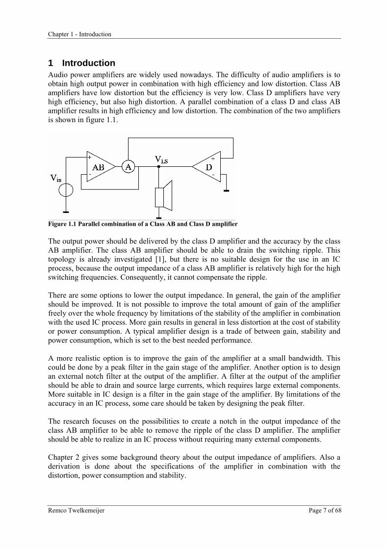
1 Introduction Audio power amplifiers are widely used nowadays. The difficulty of audio amplifiers is to obtain high output power in combination with high efficiency and low distortion. Class AB amplifiers have low distortion but the efficiency is very low. Class D amplifiers have very high efficiency, but also high distortion. A parallel combination of a class D and class AB amplifier results in high efficiency and low distortion. The combination of the two amplifiers is shown in figure 1.1.
Figure 1.1 Parallel combination of a Class AB and Class D amplifier The output power should be delivered by the class D amplifier and the accuracy by the class AB amplifier. The class AB amplifier should be able to drain the switching ripple. This topology is already investigated [1], but there is no suitable design for the use in an IC process, because the output impedance of a class AB amplifier is relatively high for the high switching frequencies. Consequently, it cannot compensate the ripple. There are some options to lower the output impedance. In general, the gain of the amplifier should be improved. It is not possible to improve the total amount of gain of the amplifier freely over the whole frequency by limitations of the stability of the amplifier in combination with the used IC process. More gain results in general in less distortion at the cost of stability or power consumption. A typical amplifier design is a trade of between gain, stability and power consumption, which is set to the best needed performance. A more realistic option is to improve the gain of the amplifier at a small bandwidth. This could be done by a peak filter in the gain stage of the amplifier. Another option is to design an external notch filter at the output of the amplifier. A filter at the output of the amplifier should be able to drain and source large currents, which requires large external components. More suitable in IC design is a filter in the gain stage of the amplifier. By limitations of the accuracy in an IC process, some care should be taken by designing the peak filter. The research focuses on the possibilities to create a notch in the output impedance of the class AB amplifier to be able to remove the ripple of the class D amplifier. The amplifier should be able to realize in an IC process without requiring many external components. Chapter 2 gives some background theory about the output impedance of amplifiers. Also a derivation is done about the specifications of the amplifier in combination with the distortion, power consumption and stability.
Chapter 1 - Introduction
Remco Twelkemeijer Page 8 of 68
The output impedance of the amplifier is derived in a pole zero analysis in chapter 3. The chapter deals with the stability in combination with a notch in the output impedance. During the derivation, some limitations were derived. The results and limitations of the pole zero analysis is translated to an amplifier design. This design is done with ideal components and results in an amplifier topology and is described in chapter 4. The amplifier topology contains some ideal components which are not suitable to implement in an IC process. Especially filters with inductors are not able to implement. In chapter 5, some filters are investigated to implement the topology in an IC process. In Chapter 6, simulations are done with the parallel combination of the AB amplifier and a class D amplifier. There are four ideal amplifiers designed which will be compared with an amplifier without a notch in the output impedance. The last chapter, chapter 7 contains the conclusion of the project.

Chapter 2 - Amplifier requirements
Remco Twelkemeijer Page 9 of 68
2 Amplifier requirements The parallel combination of a class AB and class D amplifier gives some more requirements to the class AB amplifier. The amplifier should be able to remove the switching residues of the class D amplifier. The switching frequency is relatively high compared to the audio bandwidth of 20 Hz to 20 KHz. First the gain of amplifiers is described with respect to stability. The output impedance should be low to remove the switching ripple; the limitations of the output impedance of amplifiers is described next. The output impedance of the amplifier has a relation with stability which is described in paragraph 2.3. Finally, the requirements are given when the amplifier has a notch in the output impedance.
2.1 Gain in respect with stability The design of audio amplifiers is widely described in literature and is not repeated in this section. This paragraph gives only a short summary about the gain of amplifiers in respect to stability. A two stage amplifier is shown in figure 2.1.1. First the Miller capacitance Cm1 is neglected. In that case, the amplifier contains two poles which are typically close to each other. Each pole contributing 90 degrees phase shifts and consequently the amplifier asymptotically approaches 180 degrees. The magnitude and phase characteristic of the amplifier is shown in figure 2.1.3a. The two poles without the miller capacitance are described by:
LLCRpv
CRp 11
211
1 ==
Figure 2.1.1 Two stage Amplifier Applying negative feedback, a part of the output is redirected to the input. If the output is fully redirected, a voltage buffer is created which is shown in figure 2.1.2. According to the stability criterion [8], the open loop gain has to cross the unity gain bandwidth (UGB) or zero dB before the phase shift reaches 180 degrees. The amplifier as sketched above without the Miller capacitance has a phase shift of 180 degrees at UGB. The Miller capacitance is needed which introduces a dominant pole. A bode plot containing Miller compensation is shown in figure 2.1.3b. The first pole is shifted more to the left, which results in zero dB gain before the phase shift reaches the 180 degrees.
Figure 2.1.2: Voltage buffer

Chapter 2 - Amplifier requirements
Remco Twelkemeijer Page 10 of 68
Figure 2.1.3 a) Bode and phase plot b) Bode and phase plot with Miller capacitance The Miller compensation can be extended to more than two stages. Theoretically, it is possible to extend the amplifier with an infinite number of stages. In literature different methods of Miller compensation is described, but it does not result in relatively high gain for high frequencies. In the most amplifier designs, the allowed phase is less than 180 degrees at UGB. The distance between the phase at UGB and 180 degrees is called phase margin (PM). The phase margin is indicated in figure 2.1.3b. Typical phase margins are around 45 or 60 degrees [8]. The unity gain bandwidth of the amplifier of figure 2.1.1, is described by [2]:
1
1
mCgm
UGB = .
An option to improve the gain is to increase the transconductance of the output stage. The output stage of the two-stage amplifier in figure 2.1.1 is gm2. The transconductance can be increased by increasing the quiescent current in the output transistors. This current leads to more power dissipation and is not attractive in a low power audio amplifier design.

Chapter 2 - Amplifier requirements
Remco Twelkemeijer Page 11 of 68
2.2 Derivation of the output impedance The interest in this report lies on the output resistance, because reducing the output impedance will also reduce the distortion and switching ripple [1]. The relation of the distortion and the output impedance can be easily determined using figure 2.2.1.
Figure 2.2.1 Relation between distortion and output impedance The amplifier is simplified by a voltage source with a resistance in series. The error or distortion signals are described by current source at the output. The error signal could be introduced by the amplifier itself, but also by external factors for example the class D amplifier in this case. If the output impedance is zero, the error signal is shortcut by the voltage source. If the output impedance is high, the error signal can not be dissipated by the voltage source and consequently the error signal is dissipated by the load. In this situation, the unwanted error current in the load results in distortion. The output impedance of the voltage buffer of figure 2.1.2 depending on the open loop gain
is described by [4]: oc
oout A
RZ
+=
1
The resistance “Ro”, is the open loop resistance at zero Hertz. Increasing the gain, results in decreasing of the output impedance and consequently in reducing the distortion. This is true in general, but it is also shown that it is possible to decrease the output impedance keeping the same open loop gain by influence of the feed back Miller capacitances [3]. Next, the output impedance of a simple amplifier topology is derived. The amplifier is shown in figure 2.2.2, the output is fed back to the input and a current source is applied to be able to derive the output impedance. In practice, there are a lot of variations possible, but the limitations are comparable.
Figure 2.2.2 Two stage amplifier

Chapter 2 - Amplifier requirements
Remco Twelkemeijer Page 12 of 68
The output impedance can be written by [2]:
( )
⎟⎟⎠
⎞⎜⎜⎝
⎛+
⎟⎟⎠
⎞⎜⎜⎝
⎛+
++
=
1
1
111
1
11
2
11)(
m
m
m
mout
Cgms
CCRs
CCC
gmsZ
Investigation of the output impedance equations shows that it contains some constants and a pole and a zero. The pole and zero is written by:
( ) 1
11
1111
1
nm Cgmpv
CCRz −=
+−=
For high frequencies, the output impedance is written by:
( )2
11
2
11
1gmC
CCgm
Zm
mout ≈
+=∞
Independent of the poles and zeros, the output impedance for high frequencies is always approximately 1/gm2, where gm2 is the transconductance of the output stage. To have lower output impedance at low frequencies, the zero should be set lower frequencies than the pole. The corresponding graph is shown in figure 2.2.3a. Also the situation is shown in figure 2.2.3b, when the pole is set to a lower frequency than the zero. In that case, the output impedance for low frequencies is much higher than the final value of 1/gm2 for high frequencies.
Figure 2.2.3 a) output impedance with z1<p1 b) output impedance with z1>p1 The low frequency output impedance is written by:
( )121
10Rgmgm
Zout =
To have as low output impedance as possible, gm1, gm2 and R1 should be as large as possible. As described in [2], this has some limitations. Increasing the resistance, results in decreasing the place of the first zero and results in more phase shift. The phase shift in respect to stability is described in the next paragraph. The transconductance gm2 is limited by transient current and consequently by the power dissipation.

Chapter 2 - Amplifier requirements
Remco Twelkemeijer Page 13 of 68
2.3 Output impedance in respect with stability The amplifier in paragraph 2.1 contains one zero and one pole. The corresponding phase shift is shown in figure 2.3.1. The phase shift is zero degrees for low frequencies, reaches the maximum value of +90 degrees and becomes zero degrees as well to high frequencies. A positive amount of phase shift acts inductive. Loading the output with a capacitor, there is a capacitor and inductor in parallel. This could results into oscillation and consequently in instability. In this paragraph, some limitations of designing an amplifier with respect to output impedance and stability are described.
Figure 2.3.1: Phase shift of an amplifier with one pole and one zero With one zero and one pole the phase shift is always between zero and +90 degrees. In practical designs, there are more poles and zeros and consequently it is possible to reach larger phase shifts. If the phase shift becomes negative, the amplifier acts like a capacitor. Zero degrees phase shift corresponds to a resistance. If the phase shift becomes more than +90 or less as -90 degrees, a negative resistance part is introduced.
Figure 2.3.2 a) example of Zout and a Zload b) impedances written as vectors A simplification of an amplifier with a load is shown in figure 2.3.2a. The current source with output impedance in parallel corresponds to the amplifier. In figure 2.3.2b, the impedances are written as admittances. The impedance is equal to 1/admittance. The total admittance is the sum of the two vectors. If the phase of the amplifier is +90 degrees and the load is capacitive (-90 degrees) and Yout=Yload, Ytotal is zero. The output impedance is 1/Ytotal, division by zero results in oscillation. Assuming the load can be every passive load, the phase of the load is always between +/- 90 degrees. If the amplifier never reaches +/-90 degrees, it is never possible to get oscillation and stability can be guaranteed for every passive load.

Chapter 2 - Amplifier requirements
Remco Twelkemeijer Page 14 of 68
In practical amplifier designs, the amplifier is only fully stable for limited loads [5]. With fully stable, it is meant that the amplifier does not resonate. The phase shift is normally zero or higher to get low output impedance for low frequencies. Consequently, the amplifier is limited for capacitive loads. A graph is made containing plot of the output impedance of an amplifier and two impedances of two capacitances, which are 1nF and 100nF. A capacitance of 1nF lies in the resistive part of the amplifier at 150 MHz. Increasing the capacitance, results in decreasing the impedance of the capacitor to high frequencies. The 100nF capacitance lies in the inductive part of the amplifier and the amplifier could resonate.
Figure 2.3.3 Output impedance of amplifier in combination with a capacitive load The phase of the system could exceed the +90 degrees maintaining a stable system. The resistive load should be larger than the negative resistance which is created by the amplifier. If the load is 1Ω, the phase could exceed the +90 degrees between 10-100 KHz in the example of figure 2.3.3. Especially for high frequencies when the output impedance is high, the phase should be smaller than +90 degrees to guarantee a stable system. The amount of resonance is dependence on the phase of the output impedance and the load. To be able to determine the stability of a system, a step response can be applied. A step contains all the frequency components. The step response displays overshoot and ringing. An example of a step response is shown in figure 2.3.4. The graph contains 3 lines with different step responses. The first line does not have ringing at all, the second line is damped out within 10 µs and the third line has a very long ringing time. The margin of the ringing time is not determined now, but a response like ‘line 3’ is not allowed.
Figure 2.3.4 Example of a step response
Chapter 2 - Amplifier requirements
Remco Twelkemeijer Page 15 of 68
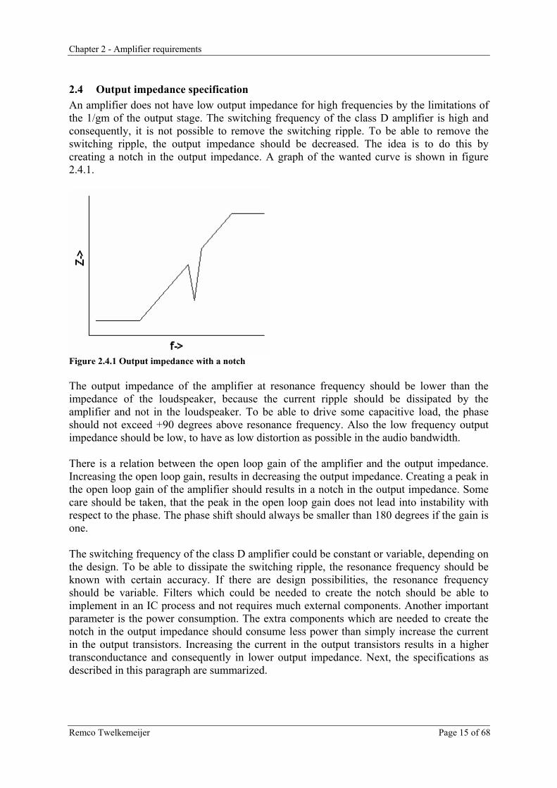
2.4 Output impedance specification An amplifier does not have low output impedance for high frequencies by the limitations of the 1/gm of the output stage. The switching frequency of the class D amplifier is high and consequently, it is not possible to remove the switching ripple. To be able to remove the switching ripple, the output impedance should be decreased. The idea is to do this by creating a notch in the output impedance. A graph of the wanted curve is shown in figure 2.4.1.
Figure 2.4.1 Output impedance with a notch The output impedance of the amplifier at resonance frequency should be lower than the impedance of the loudspeaker, because the current ripple should be dissipated by the amplifier and not in the loudspeaker. To be able to drive some capacitive load, the phase should not exceed +90 degrees above resonance frequency. Also the low frequency output impedance should be low, to have as low distortion as possible in the audio bandwidth. There is a relation between the open loop gain of the amplifier and the output impedance. Increasing the open loop gain, results in decreasing the output impedance. Creating a peak in the open loop gain of the amplifier should results in a notch in the output impedance. Some care should be taken, that the peak in the open loop gain does not lead into instability with respect to the phase. The phase shift should always be smaller than 180 degrees if the gain is one. The switching frequency of the class D amplifier could be constant or variable, depending on the design. To be able to dissipate the switching ripple, the resonance frequency should be known with certain accuracy. If there are design possibilities, the resonance frequency should be variable. Filters which could be needed to create the notch should be able to implement in an IC process and not requires much external components. Another important parameter is the power consumption. The extra components which are needed to create the notch in the output impedance should consume less power than simply increase the current in the output transistors. Increasing the current in the output transistors results in a higher transconductance and consequently in lower output impedance. Next, the specifications as described in this paragraph are summarized.

Chapter 2 - Amplifier requirements
Remco Twelkemeijer Page 16 of 68
Specifications
• The amplifier should be stable • Low output impedance in the audio bandwidth • Zout(ωpeak) << Zspeaker • Phase should not exceed +90 degrees above resonance frequency • The filter should be able to implement in an IC process • Power consumption should be low in comparison with increasing the
transconductance.
Chapter 3 - Output impedance using a Pole-Zero analysis
Remco Twelkemeijer Page 17 of 68
3 Output impedance using a Pole-Zero analysis This chapter gives some theory and methods about reducing the output impedance using a pole-zero analysis. First, a start is made with a standard amplifier described by a pole-zero map. Next, two poles and two zeros are added to create a notch in the output impedance. The notch gives some limitations to the output impedance. An approach while the last pole is neglected is first described. Next, the output impedance is investigated in a realistic situation, when the last pole is not neglected. Finally two examples of two system designs with respect to the tradeoff between the place of the poles and zeros is described.
3.1 Standard amplifier In this chapter the output impedance is derived in a very mathematical way. This means, there is a direct relation with an amplifier but the variables, poles and zeros can be set to every value. With this approach it is possible to determine the limitations about reducing the output impedance without using amplifier topologies. Designing an amplifier, it should deal with those limitations. The amplifier should have low output impedance at low frequencies as well as a certain resonation frequency. Starting with the amplifier in paragraph 2.1 of figure 2.1.1, the output impedance is described with some constants, one pole and one zero. Simplifying the output impedance to a general first order Laplace function, the output impedance is written by:
( ) ( )( )1
1
pszsKsZout −
−⋅=
K A certain proportionality factor for the output impedance. z1 First zero
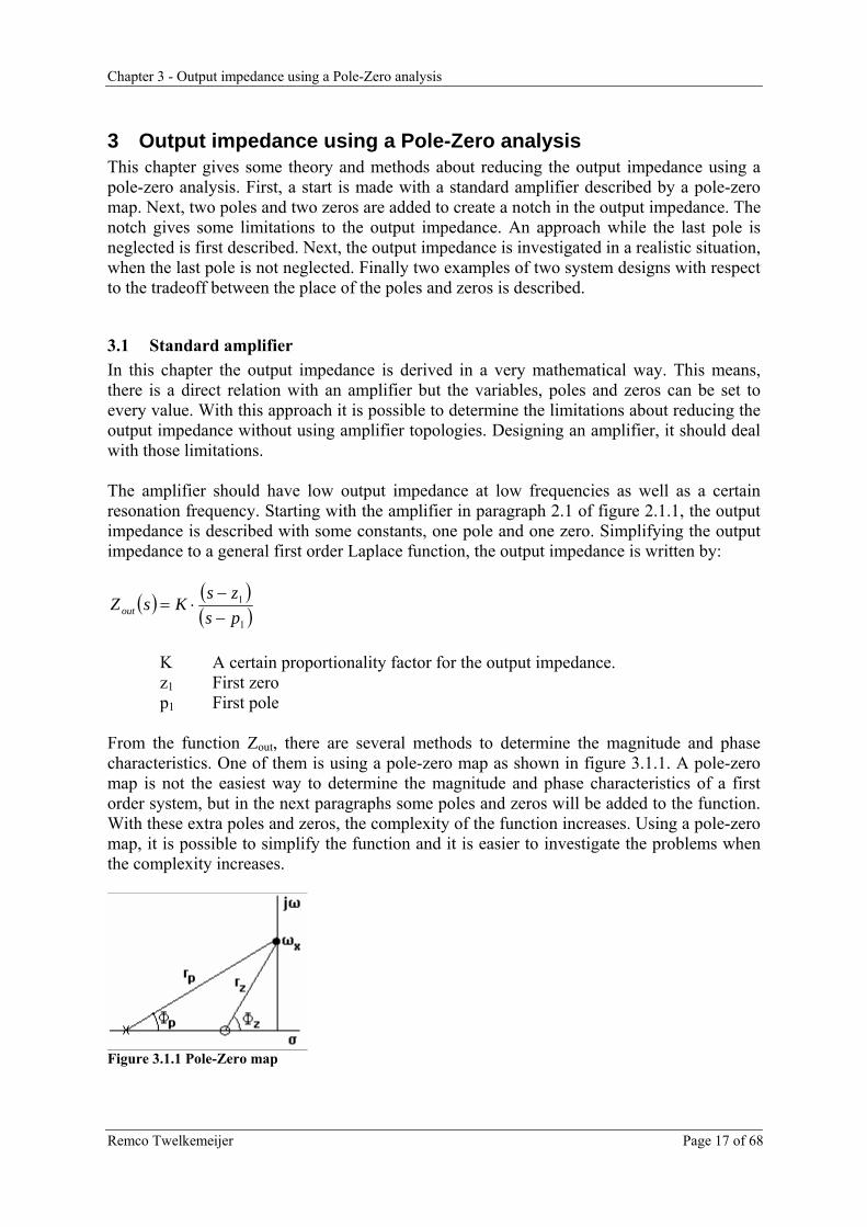
p1 First pole From the function Zout, there are several methods to determine the magnitude and phase characteristics. One of them is using a pole-zero map as shown in figure 3.1.1. A pole-zero map is not the easiest way to determine the magnitude and phase characteristics of a first order system, but in the next paragraphs some poles and zeros will be added to the function. With these extra poles and zeros, the complexity of the function increases. Using a pole-zero map, it is possible to simplify the function and it is easier to investigate the problems when the complexity increases.
Figure 3.1.1 Pole-Zero map

Chapter 3 - Output impedance using a Pole-Zero analysis
Remco Twelkemeijer Page 18 of 68
The output impedance at a frequency ωx is equal to the length of the vector of the zero divided by the length of the vector of the pole. The phase at this frequency is the angle of the vector of the zero Φz, minus the angle of the vector of the pole Φp.
( ) ( )( ) ( )( ) ( ) ( )ωωωωω
ω 111
1 , pzoutz
p
x
xxout Z
rr
Kpjzj
KZ Φ−Φ=Φ⋅=−
−⋅=
The length of the pole or zero is described as function of the frequency. It is the length of the vector from a pole or zero to a certain frequency. In figure 3.1.1, the length of the pole at frequency ωx is rp. Sometimes, the length of the vector is needed when the frequency is zero. This is described as the length at DC. Note that for real poles or zeros, the length at DC is equal to the poles and zeros. Starting at DC, ω is zero. The magnitude of the output impedance becomes:
( )1
10pz
KZout ⋅= . To get low impedance, it follows that the zero should be small and the
pole should be large. This corresponds to the magnitude characteristic of the output impedance as described in paragraph 2.2. The graph is repeated in figure 3.1.2.
Figure 3.1.2: Curve of the output impedance with one zero and one pole The contribution of a zero to the phase is +90 degrees and the contribution of a pole to the phase is -90 at maximum. Because the zero should be set to lower frequencies than the pole, the phase shift lies between zero and +90 degrees. Assuming the poles are real and the constant ‘K’ is one, the output impedance and phase shift depending on the frequency can be written by:
( ) ( )( ) ⎟⎟⎠
⎞⎜⎜⎝
⎛−⎟⎟
⎠
⎞⎜⎜⎝
⎛=Φ
+
+= −−
2
1
1
1
221
221 tantan,
pzZ
p
zZ outout
ωωωω
ωω
Chapter 3 - Output impedance using a Pole-Zero analysis
Remco Twelkemeijer Page 19 of 68
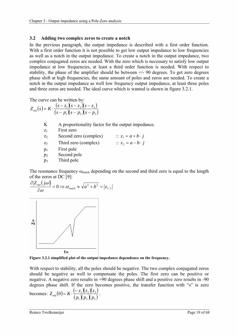
3.2 Adding two complex zeros to create a notch In the previous paragraph, the output impedance is described with a first order function. With a first order function it is not possible to get low output impedance to low frequencies as well as a notch in the output impedance. To create a notch in the output impedance, two complex conjugated zeros are needed. With the zero which is necessary to satisfy low output impedance at low frequencies, at least a third order function is needed. With respect to stability, the phase of the amplifier should be between +/- 90 degrees. To get zero degrees phase shift at high frequencies, the same amount of poles and zeros are needed. To create a notch in the output impedance as well low frequency output impedance, at least three poles and three zeros are needed. The ideal curve which is wanted is shown in figure 3.2.1. The curve can be written by:
( ) ( )( )( )( )( )( )321
321
pspspszszszsKsZout −−−
−−−⋅=
K A proportionality factor for the output impedance. z1 First zero
z2 Second zero (complex) :: jbaz ⋅+=1 z3 Third zero (complex) :: jbaz ⋅−=2
p1 First pole p2 Second pole
p3 Third pole The resonance frequency ωnotch depending on the second and third zero is equal to the length of the zeros at DC [9]:
( )2/1
220 zbajZ
notchout =+≈⇒=∂
∂ω
ωω
Figure 3.2.1 simplified plot of the output impedance dependence on the frequency. With respect to stability, all the poles should be negative. The two complex conjugated zeros should be negative as well to compensate the poles. The first zero can be positive or negative. A negative zero results in +90 degrees phase shift and a positive zero results in -90 degrees phase shift. If the zero becomes positive, the transfer function with “s” is zero
becomes: ( ) ( )( )( )( )( )( )321
3210pppzzzKZout
−⋅= .

Chapter 3 - Output impedance using a Pole-Zero analysis
Remco Twelkemeijer Page 20 of 68
The first pole z1 has a minus sign, a minus sign in the output impedance results in -180 degrees phase shift. A phase shift of -180 degrees results in a negative impedance, which could result in instability. With this approach it can be concluded that all the poles and zeros should be negative. Starting the third order system with the resonance frequency at 1 MHz and the first zero to 10 KHz and the third pole to 100 MHz, the poles can be directly determined. In paragraph 3.1, it was obtained that the poles should be as large as possible to retain low output impedance for low frequencies. Creating large poles, for example if one pole is larger than the resonance frequency and one pole is smaller than the resonance frequency. It directly follows that the phase becomes larger than +90 degrees to frequencies larger than resonance frequency. The first zero is compensated by the first pole. At resonance frequency the phase shift is +180 degrees at maximum by the two zeros and consequently more than +90 degrees. An example with a pole at 100 KHz and a pole at 10 MHz is shown in figure 3.2.2. The phase shift has the maximum value after 1 MHz and becomes nearly 180 degrees. At this frequency the phase shift should be less than 90 degrees to be able to drive some capacitive load.
Figure 3.2.2 Combination of the notch and the first order system in a third order system The magnitude characteristic of figure 3.2.2 corresponds to the wanted curve of figure 3.2.1. With respect to stability, it is not possible to create this curve. To be able to create a stable system, the second pole should also be set to lower frequencies than the resonance frequency. This situation is shown in figure 3.2.3. The two poles are able to compensate the two complex zeros if the system is designed properly. This results automatically in +90 degrees phase shift at maximum. In paragraph 3.1, it was obtained that the poles should be as large as possible to retain low output impedance for low frequencies. With the need for stability, the poles are decreased and the output impedance at low frequencies increases.
Figure 3.2.3 simplified plot of the output impedance dependence on the frequency.

Chapter 3 - Output impedance using a Pole-Zero analysis
Remco Twelkemeijer Page 21 of 68
With the first and second pole, large complex conjugated poles can be formed. This is shown in figure 3.2.4. Using the peaking behavior of the complex poles; it is possible to satisfy good output impedance at DC and a phase shift between +90 and -90 degrees. For low frequencies and keeping the real value of the poles constant, the vector of the two poles becomes larger if the poles complexity increases. Increasing the lengths of the poles, results in decreasing of the output impedance. From this approach it can be concluded that a peaking in the output impedance is needed if the low frequency output impedance has to be decreased.
Figure 3.2.4 simplified plot of the output impedance dependence of the frequency.

Chapter 3 - Output impedance using a Pole-Zero analysis
Remco Twelkemeijer Page 22 of 68
3.3 Limitations while neglecting the third pole It is seen that that the need for stability results in an increase of the output impedance for low frequencies or introduce a peak in the output impedance. One could ask how much the output impedance increase and how large should the peak in the output impedance be with a marginal lost in DC gain. In this paragraph, a derivation is done while the influence of the third pole is neglected. First the values of the poles are calculated to satisfy a stable system. Finally, the poles are supposed to be real. If the poles are real, they could be set to different frequencies. A calculation is done what happens to the output impedance at low frequencies as well at resonance frequency.
3.3.1 Length of the two poles with respect to DC With respect to stability, the values of the poles are limited by the zeros. Next these values will be calculated. The output impedance for a third order system with the constant ‘K’ is one can be written as:
( ) ( ) ( ) ( )( ) ( ) ( )ωωω
ωωωω321
321
ppp
zzz
rrrrrrH⋅⋅⋅⋅
=
The length of the poles is written by:
( ) ( ) ( )( ) ( ) ( ) 220Im22 ImRe ωωωω +=⎯⎯⎯ →⎯−+= =yxyx
pyxyxyx prppr yx
The angle is determined by subtracting the angle of the poles and adding the angle of the zeros which results in:
( )( ) ( ) ( ) ( ) ( ) ( ) ( )ωωωωωωω 321321 pppzzzZ Φ−Φ−Φ−Φ+Φ+Φ=Φ The angle of the poles is written by:
( ) ( )( )
( ) ( ) ⎟⎟⎠
⎞⎜⎜⎝
⎛=Φ⎯⎯⎯ →⎯⎟⎟
⎠
⎞⎜⎜⎝
⎛ −=Φ −=−
xpx
p
x
xpx pp
px
ωωωω 10Im1 tanRe
Imtan
The magnitude of the function corresponds to certain output impedance and should be as small as possible. The length of the poles should be as large as possible and the length of the zeros should be as small as possible. The place, and consequently the length of the poles and zeros are limited by the allowed phase shift. Starting again with the wanted curve shown in figure 3.2.1, the formula for the phase and magnitude can be simplified. Using a resonance frequency of 1 MHz, the first zero z1, is far away (for example 10Khz). The contribution of this zero results in +90 degrees phase shift. The third pole p3 is set to very high frequencies (for example 100MHz) which results in a contribution of zero degrees phase shift. The phase of the function can now be written as:
( )( ) ( ) ( ) ( ) ( )ωωωωω 213290 ppzzZ Φ−Φ−Φ+Φ+°≈Φ .

Chapter 3 - Output impedance using a Pole-Zero analysis
Remco Twelkemeijer Page 23 of 68
In the calculations, the +90 degrees is left out. To maintain +/- 90 degrees phase shift, the phase shift should be between -180 and 0 degrees. Also the contribution in magnitude of the first zero and last pole could be left out. This results in losing the low output impedance in the graphs, but the transfer function is still useful and simpler to read. If the transfer function becomes less than zero dB, there is some improvement and if the function becomes larger as zero dB the output impedance is decreased. The simplified output impedance is written as:
( ) ( ) ( )( ) ( )ωω
ωωω21
32
pp
zz
rrrrH⋅⋅
=
As described in paragraph 3.3.2, the two poles should have a smaller length than the zeros. This results in increasing the output impedance at low frequencies. Next, it is possible to calculate the influence of the place of the poles and zeros. Starting with complex conjugated zeros and complex conjugated poles, the real part of the poles can be derived to maintain a stable system.
Figure 3.3.1 Pole-Zero map In figure 3.3.1, a pole-zero map containing two complex zeros and the place of the resonance frequency on the imaginary axis is given. On the imaginary axis there is a second point, described as ‘x·ωp’. The variable ‘x’ is only a multiply factor and ωp is the resonance frequency. The contribution of the first pole to the phase of the system dependence on the variable ‘x’ can be described as:
( ) ⎟⎟⎠
⎞⎜⎜⎝
⎛ +⋅=Φ −
)Re()Im(
tan1
111 z
zxx p
z
ω
An example of the phase characteristics depending on the variable ‘x’ is shown in figure 3.3.2. The phase should be limited to -180 and zero degrees. At ‘x’ is 0.1, the phase is -180 degrees, around ‘x’ is one (resonation frequency), the phase goes to zero degrees. It reaches zero degrees asymptotically at ‘x’ infinity. In the calculations, the value ‘x’ should be large.

Chapter 3 - Output impedance using a Pole-Zero analysis
Remco Twelkemeijer Page 24 of 68
Figure 3.3.2 Phase characteristics depending on ‘x’. If ‘x’ becomes large (larger than 10), the contribution of the imaginary part to the phase becomes very small. The phase for two poles and two zeros should be between -180 and zero degrees. The contribution of the two poles can be equal to the contribution of the two zeros at high frequencies, to high values of ‘x’. The angle should be limited by:
0)Re(
)Im(tan
)Re()Im(
tan)Re(
)Im(tan
)Re()Im(
tan2
21
1
11
2
21
1
11 ≤⎟⎟⎠
⎞⎜⎜⎝
⎛ −⋅−⎟⎟⎠
⎞⎜⎜⎝
⎛ +⋅−⎟⎟⎠
⎞⎜⎜⎝
⎛ −⋅+⎟⎟⎠
⎞⎜⎜⎝
⎛ +⋅−−−−
ppx
ppx
zzx
zzx pppp ωωωω
If ‘x’ is much larger than ‘1’, the imaginary part can be neglected. The formula can be simplified to:
)Re()Re()Re()Re()Re(
tan2)Re(
tan2 11111
1
1
1 pzp
xz
xp
xz
x pppp ≥⇒⋅
≤⋅
⇒⎟⎟⎠
⎞⎜⎜⎝
⎛ ⋅≤⎟⎟
⎠
⎞⎜⎜⎝
⎛ ⋅ −− ωωωω
The real part of the zero should always be larger or at least equal as the real part of the pole. This solution is useful if the contribution of the phase of the poles should always be larger or at least equal than the contribution of the zeros. In a third order system, the phase can be larger by the influence of the first zero and third pole. The solution for this situation is described in paragraph 3.4. With the result that the real part of the zero should be larger or equal to the real part of the pole, it is possible to make a graph of the improvement in the output impedance. The graph is shown in figure 3.3.3 and contains 4 curves, two solid lines and two dotted lines. The two solid lines correspond to a system were the poles only contains a real part. The curve at DC and at resonance frequency is given. It shows clearly that if the zeros are very complex, the improvement at resonance frequency is nearly 80 dB. The improvement at DC is -160dB, which corresponds to an increase in output impedance with 160dB to low frequencies. This is unacceptable; also if the zeros become less complex the loss at DC is approximately 40dB. The dotted curves corresponds to a system containing two poles with a real part equal to the zero, but an imaginary part is introduced to keep the loss 3dB for low frequencies. Comparing the two curves at resonance frequency, the improvement at resonance frequency is decreased by approximately 10dB, but the loss is at low frequencies is only 3 dB.

Chapter 3 - Output impedance using a Pole-Zero analysis
Remco Twelkemeijer Page 25 of 68
Figure 3.3.3 Improvement of the output impedance
3.3.2 Shifting one real pole If the poles are complex, the real part of the poles is equal. Non complex poles have the possibility to have some “distance” between the poles. An example of three magnitude bode plots are shown in figure 3.3.4. The first pole is kept on the same place and the second pole is shifted to the left. This results in increasing the output impedance to low frequencies. The question is how much will the output impedance increase and what happens around the resonation frequency. A pole-zero map is shown in figure 3.3.5. It contains two complex zeros and two real poles. Starting at a point where the two poles are equal, the second pole can be decreased to zero at least. If the second pole decreases and the first pole is kept constant, the contribution of the poles to the phase is increases. From this, it follows that the complexity of the zeros can be increased and consequently the real part of the complex conjugated zeros can be decreased.
Figure 3.3.4 Magnitude plots with different distances between the poles The angle should be limited by:
⎟⎟⎠
⎞⎜⎜⎝
⎛⋅
⋅−⎟⎟
⎠
⎞⎜⎜⎝
⎛ ⋅=⎟⎟
⎠
⎞⎜⎜⎝
⎛ −⋅+⎟⎟⎠
⎞⎜⎜⎝
⎛ +⋅−−−−
1
1
1
1
2
21
1
11 tan)
tan)Re(
)Im(tan
)Re()Im(
tanp
xp
xz
zxz
zx pppp
γωω
βω
βω
Two new variables are introduced in this formula. The first one γ, is the decreasing factor of the second pole with respect to the first pole. The second pole is now described by p2= γ·p1. The range for γ could be one to zero. Starting with a γ of one and decreasing this value, the real part of the complex conjugated zeros can be decreased keeping the phase between +/- 90 degrees. This is done by the second new variable β.

Chapter 3 - Output impedance using a Pole-Zero analysis
Remco Twelkemeijer Page 26 of 68
Figure 3.3.5 Pole-Zero map with two real poles and two complex zeros Using the formula of the angle limitation, it is possible to solve the value for β. This results
in: ( ) ( )γβγβ +≈⇒>>+⎟⎠⎞
⎜⎝⎛ −≈ 1
)Re(1,111
)Re( 1
12
1
1
zp
xxz
p
The output impedance, dependence from ω can be written as the length of the zeros divided by the length of the poles. In general, the output impedance can be written for every second order system with two complex zeros and two real poles by:
( ) ( ) ( )22
222
1
22
22
21
21
21
21 )Im()Re()Im()Re(
ωω
ωωω
++
++−+==
pp
zzzzK
rrrr
KZpp
zzout
Putting the two poles and zeros in the formula and the constant factor ‘K’ is one, the follow function is obtained at resonance frequency:
( ) ( )
( )( )221
2221
22
1222
1
22
1222
1 )Re()Re()Re()Re(),(
pp
pppp
pout pp
zzzzZ
ωγω
ωβωβωβωβγω
++
⎟⎠
⎞⎜⎝
⎛⎟⎠⎞⎜
⎝⎛ +⋅−−⋅⎟
⎠
⎞⎜⎝
⎛⎟⎠⎞⎜
⎝⎛ +⋅−+⋅
=
The influence of the third pole is neglected in this approach, consequently the interest lies on
large values of ‘x’. For large values of ‘x’ and using ( )γβ +≈ 1)Re( 1
1
zp , the formula can be
simplified to:
( )1)Re(2),( 1 +⋅⋅≈ γϖ
γωp
poutpZ
Next, the output impedance can be compared with respect to γ is one (the first pole is equal to the second pole). This gives a relative improvement or reduction in the output impedance at resonance frequency, depending on the place of the second pole.
( ) 10,1
2),(
)1,(≥>
+≈ γ
γγω
ω
pout
pout
Z
Z

Chapter 3 - Output impedance using a Pole-Zero analysis
Remco Twelkemeijer Page 27 of 68
A graph of this formula is made and is shown in figure 3.3.6. Also a graph of the improvement in output impedance for low frequencies is given. For low frequencies, there is no improvement at all because the improvement factor is lower than one. It is clearly visible that if γ is approximately 0.1 (p2= 0.1·p1), the low frequency performance is decreased by 20dB and the benefit at resonance frequency is approximately 6 dB.
Figure 3.3.6 Improvement at resonate frequency and reduction at low frequencies. Result In general the output impedance around resonance frequency is improved if the second pole becomes smaller keeping the first pole constant. The output impedance at low frequencies increases too much, which is unacceptable. It can be concluded from figure 3.3.3 in paragraph 3.3.1 in combination with the approach in this paragraph, that the poles should be complex to maintain low output impedance for low frequencies. The real value of the poles should be equal or smaller than the real value of the zeros under the condition that the last pole is neglected.

Chapter 3 - Output impedance using a Pole-Zero analysis
Remco Twelkemeijer Page 28 of 68
3.4 Limitations in a realistic situation The approach while the last pole is neglected shows clearly the limitations of a notch filter. The poles should be complex to maintain low output impedance for low frequencies. Applying a step response to a system with two complex poles, resonance occurs. It seems not possible to design an amplifier without any resonation if it should have a notch and low output impedance at low frequencies and be stable for any passive load. One could ask, how complex should the poles be, using a good low frequency behavior and a deep notch. The phase limitation lies on high frequencies in paragraph 3.3.1. A practical value of the last pole could be around 10 MHz. It is not allowed to neglect the influence of the last pole with this value. The phase influence by the last pole is described by α. Next, the minimum complex conjugated poles will be simulated depending on the complex conjugated zeros and the variable α. The contribution of the first zero is 90 degrees again. This results in a phase of:
( )( ) ( ) ( ) ( ) ( ) °−Φ−Φ−Φ+Φ+°≈Φ αωωωωω 213290 ppzzZ The poles and zeros have a real and imaginary part. The resonate frequency (notch) is set to 1MHz. The resonate frequency of the poles (peak) should be smaller as 1MHz to maintain a system between +/- 90 degrees. This results in a loss of performance in the low frequency region. The length of the poles is set to a loss of 3dB in the output impedance at low frequencies. The length of the zeros divided by the length of the poles at ω=0 results in the loss in output impedance at low frequencies. A loss of 3dB and a resonate frequency of 1MHz results in the length of the poles:
( )( ) 42
2
2212321)0( ππ ⋅
=⇒==⋅
=MhzLdB
LMhzH poles
poles
With the length of the poles and zeros known, the poles and zeros are described by:
( ) ( )
( ) ( )22/1
22/12/12/1
22/1
22/12/12/1
ReRe
ReRe
pLjppLp
zjzzz
polespoles
notcnotch
−⋅±=⇒=
−⋅±≈⇒≈ ωω
Complex poles means resonation, if the poles become more complex, the resonance increases. The real part of the poles should be as large as possible to have as less resonation as possible. The phase of the system should be between +/-90 degrees, especially to high frequencies. Using this limitation, the maximum real part of the poles can be calculated dependence on the real values of the zeros. In this approach with the extra variable the angle α, it is not possible to solve the place of the poles depending on the zeros mathematically. But using the values of 1 MHz for the resonate frequency a loss of 3dB in the output impedance at low frequencies; it is possible to solve the equations numerically. In figure 3.4.1, four curves are shown, a real value of the zero of 103·2π, 104·2π, 105·2π and the maximum real value of the pole which is possible. The maximum real value of the pole is plotted dependence on the angle α. During the calculations, the length of the poles and zeros is kept constant.

Chapter 3 - Output impedance using a Pole-Zero analysis
Remco Twelkemeijer Page 29 of 68
Starting at α is zero, the corresponding real part of the poles are the same as the real part of the zeros. This proves that the calculations in paragraph 3.3.3 are correct, because the conclusion was )Re()Re( 11 pz ≥ under the condition α is zero which was not jet introduced at that moment. The graph shows a large increase in the real part of the pole to low values of α. When α becomes 5 to 10 degrees, the real part of the poles does not increase very vast anymore. The curve “maximum” value is equal to the length of the poles. The real part of the poles can never be larger as this value. At α is 45 degrees, none of the three curves will reach this maximum value of σp. From this, it can be concluded again that the poles are always complex and there will always be some ringing when applying a step response to the system.
Figure 3.4.1 Maximum real value of poles depending on the extra phase variable α In figure 3.4.2 a typical magnitude plot of the second order system is shown. There are three amplitudes given: ALF, Apeak and Anotch. This means the loss in output impedance in the low frequency region, the relative amplitude of the peak and the relative amplitude of the notch. Because the third order system is approached by a second order system with an extra phase variable α, the output impedance is zero dB to high frequencies and the loss value for low frequencies.
Figure 3.4.2 Different calculated amplitudes

Chapter 3 - Output impedance using a Pole-Zero analysis
Remco Twelkemeijer Page 30 of 68
Next, the amplitude of the second order function dependence on an extra phase is calculated. The results are shown in figure 3.4.3. It shows that an increase of the real value with a factor of 10, the notch decreases with a factor of 10. The difference of zero degrees and 45 degrees extra phase is approximately a factor of two at maximum. Extra phase does not result in a big improvement in the amplitude of the notch.
Figure 3.4.3 Anotch dependence of extra phase variable α In figure 3.4.4 the amplitude of the peak is shown. The peak should be as low as possible to have as less as possible resonation. The graph shows a large decrease in the peak value dependence by increasing α. For example, if σz is 103·2π, the peaking with α is zero degrees is more as 100. Increasing α to 20 degrees, the peaking left is only a factor of three. The extra phase results in less peaking. This is exactly what is wanted to be able to design an amplifier with a notch in the output impedance. Especially if the zeros are large complex, the difference is very large.
Figure 3.4.4 Apeak depending of extra phase variable α The calculations with the extra phase variable α results in the conclusion, that it is possible to design a system with a deep notch and a peak. The amplitude of the peak does not have to be as large as the notch if the system is designed in that way. With extra phase, it is not possible to compensate the loss in the low frequency region.

Chapter 3 - Output impedance using a Pole-Zero analysis
Remco Twelkemeijer Page 31 of 68
3.5 System Design With these results, it is possible to do a system design. A pole-zero map is made as shown in figure 3.5.1. In the map, there are also a pole and zero which results in low frequency gain. There is also a magnitude and phase plot in the figure. Those plots contain two curves, a dotted and solid line. The dotted line corresponds to a system which only has one pole and zero for the low frequency gain. This is putted in the graph for comparison purposes. The solid line has the same pole and zero as the system of the dotted line, but this system has also two complex poles and zeros to create to notch. The pole-zero map describes the system with the solid line. The zero is set to 104 Hz and the pole to 3106 Hz. This results in 70 degrees at 1 MHz as can be read in the dotted line in the phase plot. This gives 20 degrees phase. From figure 3.4.1, it can be read that with a real value of 103·2π of the zero results in approximately a real value to the pole of 7104·2π. From figure 3.4.3 it can be read that the improvement at 1 MHz is approximately 0.006 (-44dB). The amplitude of the peak is approximately a factor of three (9,5dB) which can be read from figure 3.4.4. The magnitude plot in figure 3.3.14 shows that these values correspond.
Figure 3.5.1 Pole-Zero map with corresponding magnitude and phase characteristics Another option is to decrease the phase of the system as shown in figure 3.5.2. The zeros are on the same place but the last pole is set to 3107·2π. To maintain a system between +/- 90 degrees phase shift, the real part of the complex poles should decrease to 3103·2π. This decrement result in a larger peak, but with approximately no change to the notch.
Figure 3.5.2 Pole-Zero map with corresponding magnitude and phase characteristics

Chapter 3 - Output impedance using a Pole-Zero analysis
Remco Twelkemeijer Page 32 of 68
For the systems of the pole zero maps as described in figure 3.5.1 and figure 3.3.2, a step response is applied. The result is shown in figure 3.5.3, the solid line correspond to the pole-zero map in figure 3.5.2 and the dashed line to the pole-zero map of figure 3.5.1. The placement of the last pole of the two systems differs, and consequently the gain. This results in a different maximum value of overshoot. To compare those two systems, the maximum amplitude of overshoot of the response is normalized. Comparing the two curves, the damping of the system with the higher real value is much larger and the step response becomes nearly zero within 10 μs. The other curve has low damping factor, which results in a very long ringing time.
Figure 3.5.3 Step response corresponding to the two pole-zero maps.

Chapter 4 - Amplifier design
Remco Twelkemeijer Page 33 of 68
4 Amplifier design The approach in the previous chapter determines the theoretical limitations of the amplifier. In this chapter practical topologies are described to create a notch in the output impedance. First the system implementation is described briefly. Next the topology of an amplifier to create a notch in the output impedance is described. With this amplifier a system design is done. Finally an implementation is done with a output stage.
4.1 System Implementation In the previous chapter it is determined that at least a third order output impedance is needed to create a notch in the output impedance. The output impedance should contain two complex poles and two complex zeros with one real pole and zero. Simplifying every amplifier stage as blocks, the amplifiers can be set in cascade or in parallel as shown in figure 4.1.1a and figure 4.1.1b respectively. In [2] it is proven with simulations that adding an extra cascade stage normally results in an extra pole and zero. This is under the assumption that the extra stage contains a capacitance and a resistance which is a first order function. From this, one of the two stages of the amplifier should contain two complex poles and two complex zeros if the amplifiers are set in cascade.
( )( )
( )( )( )( )
( )( )
( )( )( )( )32
32
1
11
32
32
1
11
pspszszs
pszsZZZ
pspszszs
ZvpszsZ
notchcascade
notch
−−−−
⋅−−
=⋅=
−−−−
=−−
=
Creating two amplifiers with only one stage, the output impedance of the two amplifiers are set in parallel. If the first amplifier has one pole and one zero and the second one has only two complex zeros and two real poles, the output impedance is written by a third order function which contains 2 complex poles and two complex zeros. This can be obtained from the formula Zparallel, the denominator contains the zeros z2 and z3 which are assumed to be complex. Solving the values of the three poles in the denominator, one real pole and two complex poles is obtained.
( )( )( )
( )( )( ) ( )( )( )132321
321
1
11 //
zspspszszspszszszs
ZZZZ
ZZZnotch
notchnotchparallel −−−+−−−
−−−=
+⋅
==
It seems easier to implement two amplifiers in parallel, because only two complex zeros should be created. Another reason could be that the first amplifier contains always a linear path, while the second amplifier can be designed with time discrete section in it without aliasing problems.
Figure 4.1.1 a) Amplifiers in cascade b) Amplifiers in parallel
Chapter 4 - Amplifier design
Remco Twelkemeijer Page 34 of 68
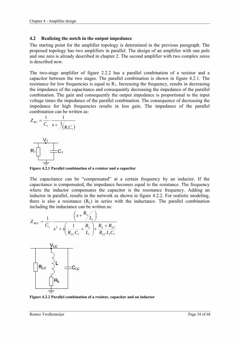
4.2 Realizing the notch in the output impedance The starting point for the amplifier topology is determined in the previous paragraph. The proposed topology has two amplifiers in parallel. The design of an amplifier with one pole and one zero is already described in chapter 2. The second amplifier with two complex zeros is described now. The two-stage amplifier of figure 2.2.2 has a parallel combination of a resistor and a capacitor between the two stages. The parallel combination is shown in figure 4.2.1. The resistance for low frequencies is equal to R1. Increasing the frequency, results in decreasing the impedance of the capacitance and consequently decreasing the impedance of the parallel combination. The gain and consequently the output impedance is proportional to the input voltage times the impedance of the parallel combination. The consequence of decreasing the impedance for high frequencies results in less gain. The impedance of the parallel combination can be written as:
( )111 1
11
CRsCZ RC
+⋅=
Figure 4.2.1 Parallel combination of a resistor and a capacitor The capacitance can be “compensated” at a certain frequency by an inductor. If the capacitance is compensated, the impedance becomes equal to the resistance. The frequency where the inductor compensates the capacitor is the resonance frequency. Adding an inductor in parallel, results in the network as shown in figure 4.2.2. For realistic modeling, there is also a resistance (RL) in series with the inductance. The parallel combination including the inductance can be written as:
1111
2
1
1 11
CLRRR
LR
CRss
LRs
CZ
LC
LCLL
LC
L
RLC ++⎟⎟
⎠
⎞⎜⎜⎝
⎛++
⎟⎠⎞⎜
⎝⎛ +
⋅=
Figure 4.2.2 Parallel combination of a resistor, capacitor and an inductor

Chapter 4 - Amplifier design
Remco Twelkemeijer Page 35 of 68
In figure 4.2.3 two bode plots are shown of the two parallel impedances which are indicated as ZRC and ZRLC. There also three resistances given, the impedance of ZRC is equal to R1 for low frequencies. The impedance of ZRLC is RL for low frequencies and ZLC (equal to R1 in this example) at resonance frequency. The impedance at resonance frequency of the ZRLC network is much higher than the ZRC network, this result in more gain.
Figure 4.2.3 Impedances of ZRC and ZRLC It is shown that adding an inductor in parallel results in a peak in the impedance at resonance frequency. Adding the inductor in a two stage amplifier, result in the topology as shown in figure 4.2.4. In practice it is not possible to use an inductor in an integrated circuit. The design of an inductor or a second order filter in an integrated circuit is described in chapter 5. The derivation of the output impedance is described in appendix A. The contribution of the Miller capacitance at high frequencies is ignored first.
Figure 4.2.4 Two stage amplifier with a RLC filter The output impedance is written by:
( ) ( )
⎟⎟⎠
⎞⎜⎜⎝
⎛+⎟⎟
⎠
⎞⎜⎜⎝
⎛+
+
++⎟⎟
⎠
⎞⎜⎜⎝
⎛+
++
+=
1
1
1
111
1
1111
2
1
11
2
111
m
L
m
L
L
m
m
mout
Cgms
LRs
CCLR
R
LR
RCCss
CCC
gmZ
Chapter 4 - Amplifier design
Remco Twelkemeijer Page 36 of 68
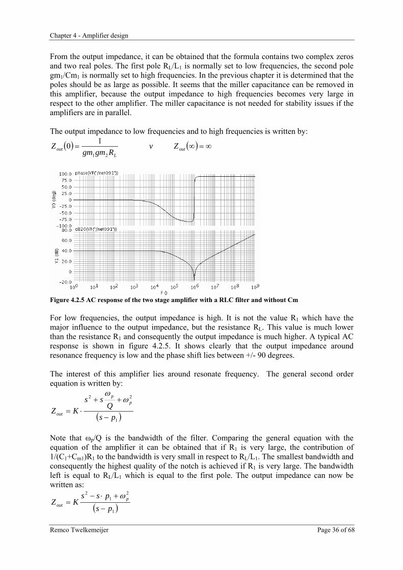
From the output impedance, it can be obtained that the formula contains two complex zeros and two real poles. The first pole RL/L1 is normally set to low frequencies, the second pole gm1/Cm1 is normally set to high frequencies. In the previous chapter it is determined that the poles should be as large as possible. It seems that the miller capacitance can be removed in this amplifier, because the output impedance to high frequencies becomes very large in respect to the other amplifier. The miller capacitance is not needed for stability issues if the amplifiers are in parallel. The output impedance to low frequencies and to high frequencies is written by:
( ) ( ) ∞=∞= outL
out ZvRgmgm
Z21
10
Figure 4.2.5 AC response of the two stage amplifier with a RLC filter and without Cm For low frequencies, the output impedance is high. It is not the value R1 which have the major influence to the output impedance, but the resistance RL. This value is much lower than the resistance R1 and consequently the output impedance is much higher. A typical AC response is shown in figure 4.2.5. It shows clearly that the output impedance around resonance frequency is low and the phase shift lies between +/- 90 degrees. The interest of this amplifier lies around resonate frequency. The general second order equation is written by:
( )1
22
psQ
ssKZ
pp
out −
++⋅=
ωω
Note that ωp/Q is the bandwidth of the filter. Comparing the general equation with the equation of the amplifier it can be obtained that if R1 is very large, the contribution of 1/(C1+Cm1)R1 to the bandwidth is very small in respect to RL/L1. The smallest bandwidth and consequently the highest quality of the notch is achieved if R1 is very large. The bandwidth left is equal to RL/L1 which is equal to the first pole. The output impedance can now be written as:
( )1
21
2
pspss
KZ pout −
+⋅−=
ω
Chapter 4 - Amplifier design
Remco Twelkemeijer Page 37 of 68
Where, the pole and resonance frequency is written by:
( )1111
11
1
mp
L
CCLv
LRp
+≈−= ω
With this approach, it can be obtained that the output impedance can only becomes zero if the first pole is zero. If the bandwidth becomes very small, it is very difficult to design the resonance frequency exactly at a certain frequency without any variations. The minimum bandwidth depends directly on how accurate it is possible to create the peak filter.

Chapter 4 - Amplifier design
Remco Twelkemeijer Page 38 of 68
4.3 Amplifiers in parallel A topology when the amplifiers are set in parallel is shown in figure 4.3.1. The output impedance is equal to the parallel impedance of the two amplifiers. The low frequency output impedance should be as low as possible. In chapter 3 it is described that a notch results in an increment in the output impedance, but this increment should be minimal.
Figure 4.3.1 Two stage amplifier The output impedance is written by:
( )( )( )( )( )( ) ( )( )( )132321
3211 //
zspspszszspszszszs
ZZZ notchparallel −−−+−−−−−−
==
The output impedance is now written in a more complex way which is not easy to solve. To see what happens, ideal simulations are done when only one component is changed. First the transconductance gmL1 is simulated with the values of 10μS, 35μS and 70μS. Values gm1 = 70 μS gmL1 = variable gm2 = gmL2 = -200μS R1 = 1.5MΩ C1 = 1pF Cm1 = 5pF CLC = 6 pF L = 4.22mH RL = 1kΩ RLC = ∞ The only frequency region where the output impedance of Znotch is lower than Z1 is around resonance frequency. Starting with a resonance frequency of 1 MHz, the two amplifiers can be compared separately. In figure 4.3.2a, three curves with a notch are shown and the last one is the output impedance of Z1 alone with gm1 is 94 μS. From the figure, it can be determined that increasing the transconductance of gmL1, results in lower output impedance around resonance frequency in comparison with Z1. The frequency when the output impedances are equal also increases with the transconductance. With gmL1=10 μS, the output impedance becomes equal around 1.1 MHz. Increasing the gmL1 to 70 μS it is increased to approximately 2 MHz.

Chapter 4 - Amplifier design
Remco Twelkemeijer Page 39 of 68
Figure 4.3.2 a) Output impedance amplifiers separately b) Output impedance amplifiers in parallel Combining the two amplifiers result in the graph as shown in figure 4.3.2b. In this graph, also four curves are shown. Three of them are the amplifier of figure 4.3.1. The last one is for comparison purposes and is only a two stage amplifier with the same values of Z1, except gm1 which is 94 μS. As can be obtained from the figure, increasing the notch in this way results in larger peaking and the output impedance is lower to high frequencies. The larger peaking results in a larger ringing time when a step response is applied. The last pole is shifted to the right when the output impedance is lower to high frequencies, because the final impedance is the same (approximately 1/gm2). Using the determined values in the simulations results in the conclusion that the third pole can be approximated by:
1
113
m
L
Cgmgmp +
−≈
The high frequency part of amplifiers is limited to be able to drive some capacitive load. Increasing the gain of the amplifier with the notch and keeping the third pole constant results in increasing of the low frequency output impedance. Another option is to increase the quality of the notch by decreasing the series resistance RL of the inductance. Simulating it with the values of 100Ω, 1kΩ and 2kΩ result in the graph as shown in figure 4.3.3a. In this graph the output impedance is determined separately again. Also the output impedance with gm1 = 94 μS is shown for comparison purposes. Values gm1 = 70 μS gmL1 = 70 μS gm2 = gmL2 = -200 μS R1 = 1.5MΩ C1 = 1pF Cm1 = 5 pF CLC = 6 pF L = 4.22mH RL = variable RLC = ∞ The figure shows clearly that increasing the quality of the notch only results in lower output impedance around 1 MHz, the high frequency behavior is the same for every quality factor. This suggests that this is also the case when the two amplifiers are combined. The graph of the amplifier is shown in figure 4.3.3b which shows that the output impedance to high frequencies is the same. The only disadvantage is that the peak becomes larger when the notch increases, but this is also expected from chapter 3.
Figure 4.3.3 a) Output impedance amplifiers separately b) Output impedance amplifiers in parallel

Chapter 4 - Amplifier design
Remco Twelkemeijer Page 40 of 68
Another important part of the stability of the amplifier is the frequency response of the open and closed loop gain. Applying a voltage source to the input and load the output with 1kΩ, results in the graph as shown in figure 4.3.4a. The gain is increased as expected at 1 MHz, which could lead to instability if the phase reaches -180 degrees. The resonance frequency results in a positive phase shift to approximately 60 degrees. The phase becomes -90 degrees after resonance frequency. This phase shift does not lead to instability. Designing the amplifier, some care should be taken at the increasing of the gain with respect to the UGB.
Figure 4.3.4 a) Open loop gain b) Closed loop gain In figure 4.3.4b, the closed loop gain of the amplifier is shown. The gain is 0dB to 1 MHz and decreases after this frequency. There is also a notch in the gain, which corresponds to the resonance frequency when a step response is applied to the amplifier. In chapter 3.4 it is seen that the increasing in the output impedance for low frequencies directly corresponds to the peaking frequency. Now, an approach is done to determine the peaking frequency. The peaking frequency and the notch is shown in figure 4.3.5. Keeping all the variables constant except gmL1+gm1, it is possible to determine a formula of the peaking frequency. Assuming the last pole is constant, gmL1+gm1 is constant. Increasing the notch, results in decreasing gm1 and consequently decreasing the peaking frequency because the low frequency output impedance is increased. With this approach and in combination with the results of chapter 3.4, the peaking frequency is written by:
gmgmgm
1L1
1
+= notchpeak ωω
Figure 3.3.5 Bode plot of the output impedance with a peak and a notch This is valid under the assumption that gm2=gmL2 and the output impedance of Zout is lower than Z1 around resonance frequency. With the results in this paragraph, a topology design can be done. Setting the first zero to 10 KHz, the resonance frequency to 1 MHz, the last pole to 3 MHz and the increasing in the output impedance to 3dB, results in the following values.

Chapter 4 - Amplifier design
Remco Twelkemeijer Page 41 of 68
Values of output impedance with notch gm1 = 66,5 μS gmL1 = 27,5 μS gm2 = gmL2 = -200μS R1 = 2.65 MΩ C1 = 1 pF Cm1 = 5pF CLC = 6 pF L = 4.22 mH RL = 500 Ω RLC = ∞ Values of output impedance without notch gm1 = 94 μS gm2 = -200μS R1 = 2.65 MΩ C1 = 1 pF Cm1 = 5 pF The magnitude and phase result of the simulation with these values is shown in figure 4.3.6a and 4.3.6b. The magnitude behavior of a two stage amplifier is also shown (gm1=94uS). The graph clearly shows the increase of 3dB to low frequencies. The peak is much smaller than the notch and the high frequency output impedance and phase are the same for both amplifiers. The peaking frequency is 835 KHz, calculating this frequency with the formula above result in 841 KHz which seems to be a good approximation. Also a pole and zero simulation is done, which shows that the calculated values are correspond to the simulated one.
Figure 4.3.6 a) Magnitude plot b) Phase plot Simulated poles and zeros p1 = -57.696 kHz + j 853.257 kHz z1 = -10.010 kHz p2 = -57.696 kHz - j 853.257 kHz z2 = -9.429 kHz + j 1.000 MHz p3 = -2.897 MHz z3 = -9.429 kHz – j 1.000 MHz
Chapter 4 - Amplifier design
Remco Twelkemeijer Page 42 of 68
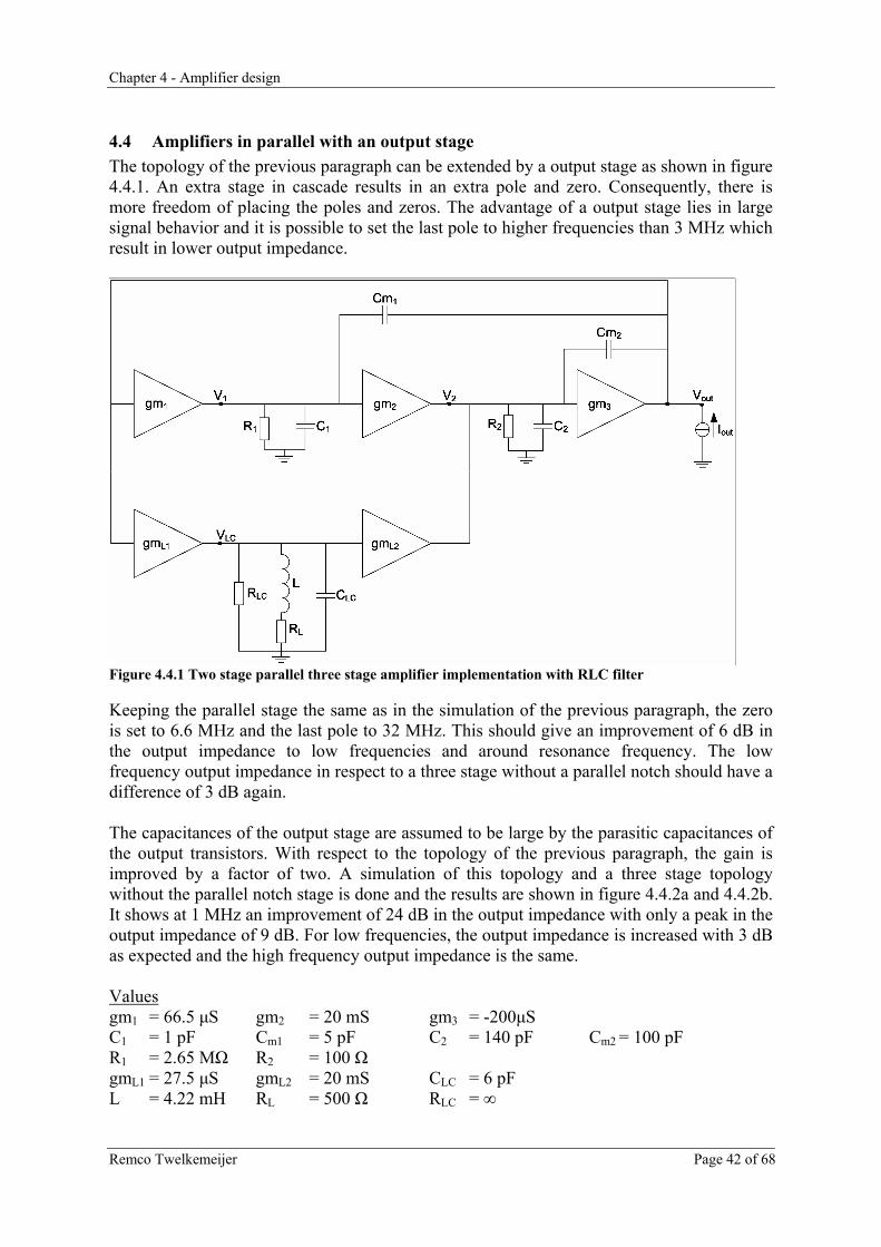
4.4 Amplifiers in parallel with an output stage The topology of the previous paragraph can be extended by a output stage as shown in figure 4.4.1. An extra stage in cascade results in an extra pole and zero. Consequently, there is more freedom of placing the poles and zeros. The advantage of a output stage lies in large signal behavior and it is possible to set the last pole to higher frequencies than 3 MHz which result in lower output impedance.
Figure 4.4.1 Two stage parallel three stage amplifier implementation with RLC filter Keeping the parallel stage the same as in the simulation of the previous paragraph, the zero is set to 6.6 MHz and the last pole to 32 MHz. This should give an improvement of 6 dB in the output impedance to low frequencies and around resonance frequency. The low frequency output impedance in respect to a three stage without a parallel notch should have a difference of 3 dB again. The capacitances of the output stage are assumed to be large by the parasitic capacitances of the output transistors. With respect to the topology of the previous paragraph, the gain is improved by a factor of two. A simulation of this topology and a three stage topology without the parallel notch stage is done and the results are shown in figure 4.4.2a and 4.4.2b. It shows at 1 MHz an improvement of 24 dB in the output impedance with only a peak in the output impedance of 9 dB. For low frequencies, the output impedance is increased with 3 dB as expected and the high frequency output impedance is the same. Values gm1 = 66.5 μS gm2 = 20 mS gm3 = -200μS C1 = 1 pF Cm1 = 5 pF C2 = 140 pF Cm2 = 100 pF R1 = 2.65 MΩ R2 = 100 Ω gmL1 = 27.5 μS gmL2 = 20 mS CLC = 6 pF L = 4.22 mH RL = 500 Ω RLC = ∞

Chapter 4 - Amplifier design
Remco Twelkemeijer Page 43 of 68
Values for comparison gm1 = 94 μS gm2 = 20 mS gm3 = -200μS C1 = 1 pF Cm1 = 5 pF C2 = 140 pF Cm2 = 100 pF R1 = 2.65 MΩ R2 = 100 Ω
Figure 4.4.2: a) Magnitude plot b) Phase plot Simulated poles and zeros p1 = -58.425 kHz + j 851.777 kHz z1 = -10.010 kHz p2 = -58.425 kHz - j 851.777 kHz z2 = -9.429 kHz + j 1.000 MHz p3 = -3.350 MHz z3 = -9.429 kHz - j 1.000 MHz p4 = -27.815 MHz z4 = -6.631 MHz p5 = -185.382 MHz At high frequencies (higher than 100 MHz), the output impedance shows a capacitive behavior. This corresponds to the fifth pole which is equal to 185 MHz. The pole is introduced by the high frequency influence of the miller capacitance. During the derivation of the output impedances in this report, the high frequency influence of the miller capacitance is always neglected. In practice the influence of this capacitance introduce an extra pole and could lead to instability [2]. The extra pole can be approximated by the intersection between the resistive part and the miller capacitance. The resistive part is the output impedance at high frequencies. The pole can be approximated by:
22
3
1
11
2
11
1 m
mmiller
mm
m
CCg
psCC
CCgm +
−=⇒≡+
A bode plot of the output impedance including the extra pole is shown in figure 4.4.3a. In this plot, the first pole and the pole of the miller capacitance are far away. Starting at low frequencies, this results in a resistive part, inductive part, a resistive part again and finally capacitive respectively.
Figure 4.4.3 a) Bode plot when pm>>p1 b) Bode plot when pm and p1 are complex

Chapter 4 - Amplifier design
Remco Twelkemeijer Page 44 of 68
The pole pm is an approximation which is valid if the poles are far away from each other. If the become closer to each other, the complete derivation should be done. The derivation is also done in [2]. The interest lies on the high frequencies and consequently on the two poles. The two poles are written by:
⎟⎟⎠
⎞⎜⎜⎝
⎛⋅⋅
−⎟⎟⎠
⎞⎜⎜⎝
⎛ −±
−−=
11
21
2
1
12
1
121 22
/CmCgmgm
Cgmgm
Cgmgm
pp m
From the two poles, it can be obtained that if the value of gm1 is close to gm2, complex poles are formed. A bode plot of the output impedance is shown in figure 4.4.3b when the poles are complex. The complex poles results in a peak in the output impedance, which results in resonation if a step response is applied. If gm1 becomes larger than gm2 the complex poles becomes positive, which causes the amplifier to be unstable. The complexity depends on how close gm2 and gm1 are. The output impedance for the two simulated amplifiers (with and without a notch in the output impedance) is the same for high frequencies. This results also in the same last pole and the same requirements to maintain a stable system.

Chapter 5 - Filter implementation
Remco Twelkemeijer Page 45 of 68
5 Filter implementation In the previous chapter, inductors are used in the amplifier. It is impossible to create inductors in an IC process, if the inductor should work around the frequencies of interest. This problem can be solved by filters which should have the same behavior as the function described in chapter 3 and 4. First, a start is made with continuous time filters to implement a filter in the amplifier. Finally switched capacitor filters are described in respect with some relevant amplifier topologies.
5.1 Continuous time filters The easiest way is to create a peak filter is an active component which acts like an inductor, This could be done by a gyrator loaded by a capacitor. A gyrator is an active component which gyrate a current into a voltage and a voltage into a current. Loading the gyrator results in an inverse capacitor which is actually a inductor. The inductor can just be replaced by the gyrator in the amplifier topology of figure 4.2.4. A traditional gyrator loaded with a capacitor is shown in figure 5.1.1. The impedance of the active inductor is written by:
eqinductor LsLsZ ⋅≡⋅=
Figure 5.1.1 Gyrator loaded with a capacitor using two OTAs The inductance Leq is written by [7]:
21
0
mmeq gg
CL =
The simulated inductance depends ideally on the capacitance and the two transconductance of the two Operational Transconductance Amplifiers (OTAs). Combining the simulated inductance into the formula for the resonance frequency:
10
21
1
1CCgg
CLmm
eqp ==ω
In an IC process there is a large spread of the transconductance of the amplifiers. Also the absolute values of capacitances contain a large spread. The resonance frequency depends on the absolute values of the capacitances and transconductance. If the total absolute spread is approximately 50%, the resonance frequency lies between 700 KHz and 1.2 MHz. The impedance of a peak filter with this variation is shown in figure 5.1.2a. It shows clearly that the notch should be much more accurate.

Chapter 5 - Filter implementation
Remco Twelkemeijer Page 46 of 68
Figure 5.1.2 a) Peak filter with +/- 50% accuracy b) Compensated filter with +/- 20% accurcacy To reach certain accuracy in the output impedance at resonance frequency, the peak should be reduced. An example of a compensated filter with 20 percent accuracy is shown in figure 5.1.2b. The difference in output impedance at resonance frequency is approximately 6 dB. It shows also the original curve with an output impedance of 1 MΩ around resonance frequency. The difference between the curves is very large and does not satisfy the requirements of the filter. In literature several other topologies of time continuous bandwidth filters are described, but these filters requires compensation methods like external bias currents to satisfy a high accuracy [10, 11]. It is also possible to design a filter without a direct relation ship of an inductor, but these filters depend on some way on the transconductance [7]. In chapter 4 it is determined that the quality of the filter should be as high as possible. It seems that continuous time filters does not satisfy this requirement.

Chapter 5 - Filter implementation
Remco Twelkemeijer Page 47 of 68
5.2 Switched capacitor filters Switched capacitor filters are normally used in IC design and are widely described in literature. The accuracy of the filters in an IC process is much higher than continuous time filters. Switched capacitor filters can be designed in several ways. The first one which is described act like a inductor. Another possibility is to design a Laplace or Z function which can be created in some way. A filter is described when only one capacitor is used to create the notch in the output impedance. Finally, the filter is extended with more capacitors to reach a higher quality factor.
5.2.1 Component simulation In component simulation, the inductors and resistances are simulated by active or passive SC networks. The design basically consists of replacing the inductors and resistors by these simulated networks. An example of the simulation of an inductor is shown in figure 5.2.1. The equivalent inductance is written by [6]:
1
2
16 CTLeq ⋅
=
Figure 5.2.1 Simulation of an inductor In comparison with the active gyrator in chapter 5.1, the capacitance is now in the denominator. Placing a capacitance C3 between Vi and ground, a parallel combination of an inductor and capacitance is created. This results in a relative dependence of the capacitances in the resonance frequency which results in a much better accuracy in an IC-process. The resonance frequency can now be written as:
3
141CC
TLCp ⋅==ω
If the sampling frequency is 10 MHz and the capacitance C1 is 1pF, the capacitance C3 should be 40.5pF to get a resonance frequency of 1 MHz. The capacitance of C2 is also 1pF, but this capacitance does not influence the resonance frequency.
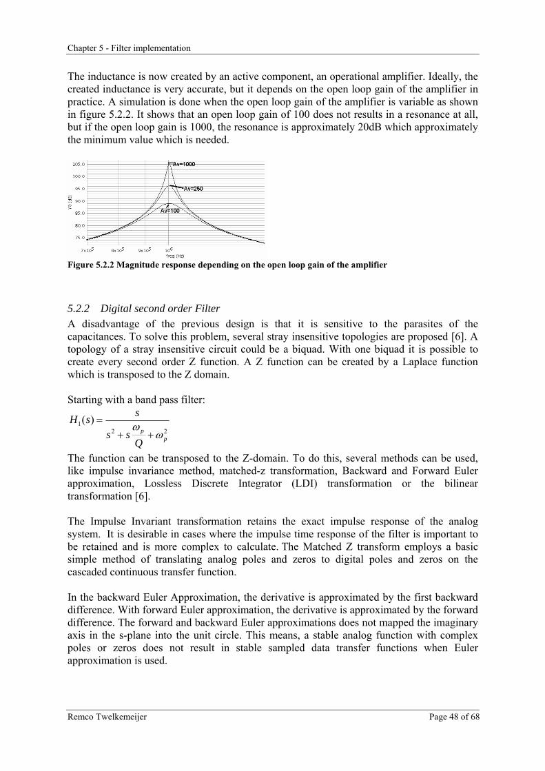
Chapter 5 - Filter implementation
Remco Twelkemeijer Page 48 of 68
The inductance is now created by an active component, an operational amplifier. Ideally, the created inductance is very accurate, but it depends on the open loop gain of the amplifier in practice. A simulation is done when the open loop gain of the amplifier is variable as shown in figure 5.2.2. It shows that an open loop gain of 100 does not results in a resonance at all, but if the open loop gain is 1000, the resonance is approximately 20dB which approximately the minimum value which is needed.
Figure 5.2.2 Magnitude response depending on the open loop gain of the amplifier
5.2.2 Digital second order Filter A disadvantage of the previous design is that it is sensitive to the parasites of the capacitances. To solve this problem, several stray insensitive topologies are proposed [6]. A topology of a stray insensitive circuit could be a biquad. With one biquad it is possible to create every second order Z function. A Z function can be created by a Laplace function which is transposed to the Z domain. Starting with a band pass filter:
221 )(
pp
Qss
ssHω
ω++
=
The function can be transposed to the Z-domain. To do this, several methods can be used, like impulse invariance method, matched-z transformation, Backward and Forward Euler approximation, Lossless Discrete Integrator (LDI) transformation or the bilinear transformation [6]. The Impulse Invariant transformation retains the exact impulse response of the analog system. It is desirable in cases where the impulse time response of the filter is important to be retained and is more complex to calculate. The Matched Z transform employs a basic simple method of translating analog poles and zeros to digital poles and zeros on the cascaded continuous transfer function. In the backward Euler Approximation, the derivative is approximated by the first backward difference. With forward Euler approximation, the derivative is approximated by the forward difference. The forward and backward Euler approximations does not mapped the imaginary axis in the s-plane into the unit circle. This means, a stable analog function with complex poles or zeros does not result in stable sampled data transfer functions when Euler approximation is used.

Chapter 5 - Filter implementation
Remco Twelkemeijer Page 49 of 68
The Bilinear uses trapezoidal integration to implement the digital Z transform. It is usually the most accurate digital implementation for filtering a continuous variable. However, significant warping of the frequency spectrum occurs. The LDI transformation is, just as the bilinear transformation, derived from trapezoidal integration method. But the LDI transformation uses midpoint integration. However, significant warping of the frequency spectrum occurs. It is not possible to do the backward and forward Euler approximation, because complex poles are needed. The bilinear and LDI transformation seems to be a good option. To solve the problem of warping of the frequency, pre-warping techniques are available for the bilinear and LDI transformation. In this paragraph, the bilinear transformation is used. Calculation of the pre-warped frequency and quality factor [6]:
( ) ( )⎟⎟⎟⎟
⎠
⎞
⎜⎜⎜⎜
⎝
⎛⎟⎠⎞
⎜⎝⎛
⋅−−
⎟⎟⎟⎟
⎠
⎞
⎜⎜⎜⎜
⎝
⎛⎟⎠⎞
⎜⎝⎛
⋅+⋅
⋅=
⎟⎟⎠
⎞⎜⎜⎝
⎛⋅⋅=
fs
Q
fs
Qfs
Q
ffs
pp
pp
pp
s
pp
2
211
tan2
211
tan
12
2tan2
\\
\\
\
ωω
ω
ωω
Setting the resonance frequency to 1 MHz and the quality of the filter to 20, a pre-warped frequency of 1,034 MHz and pre-warped quality factor of 18 is calculated. Next, the filter can be transposed by [6]:
1112)( 12
12
1
1
12 +⋅−⋅+⋅−⋅
=⎟⎟⎠
⎞⎜⎜⎝
⎛+−
⋅= −−
−−
−
−
zuzvpzqzr
zzfHzH s
In appendix B, the formulas for the variables are given. Solving the equation with a gain of 20 at resonance frequency, the formula results in:
21
2
2 968.0592.1132.032.0)( −−
−
⋅+⋅−⋅−
=zz
zzH
Figure 5.2.3 Frequency response of the Z-Filter

Chapter 5 - Filter implementation
Remco Twelkemeijer Page 50 of 68
The frequency response of the Z-filter is shown in figure 5.2.3. The graph shows clearly the resonance frequency of 1 MHz and the peak is approximately 20. Solving the capacitances in a biquad, results in the conclusion that the total capacitance is higher than 100 times the unit capacitances. This is much too high in comparison with the space which is needed for the capacitances.
5.2.3 Peak filter using one capacitor In literature, a simple but very good SC notch filter is described [12]. This filter is shown in figure 5.2.4a. The notch occurs exactly at sampling frequency. The voltage at V2 could never contain this frequency because the input voltage at V1 is every time the same. With this configuration it is very easy to control the notch frequency and the capacitance size is not very important. The transient response when the input frequency is equal to the sampling frequency is shown in figure 5.2.5a.
Figure 5.2.4 (a) SC notch filter; (b) SC peak filter. Changing the configuration into a periodically inverse capacitor as shown in figure 5.2.4b, a peak filter is created. In this case, the input is a current source at V1, V2 is grounded and the peak occurs at sampling frequency again. The idea is the same; the current over the positive half of the sine wave is integrated by the capacitor in the even phase. In the odd phase, the capacitor is inverted, and the voltage at V1 becomes negative. Together with the negative half of the sine wave, the capacitor becomes more negative. An ideal simulation is done and the result is shown in figure 5.2.5b. The graph shows an increment in the output voltage depending on the time. In comparison with the SC notch filter, this system has some disadvantages. The peak occurs exactly at Nyquist frequency and odd Harmonics of the sampling frequency will be transposed to the sampling frequency.
Figure 5.2.5 a) Transient response SC notch filter b) Transient response SC peak filter

Chapter 5 - Filter implementation
Remco Twelkemeijer Page 51 of 68
A simple amplifier topology which contains the SC peak filter of figure 5.2.4b is shown in figure 5.2.6. The resistor Rs simulates the switching resistance and is assumed to be low. Now it is possible to determine if this peak filter also generates a notch in the output impedance. Applying some current Iout to the amplifier, the voltage V1 is known because gm2 should drain this current. Switching the capacitance to the opposite direction results ideally in loading the capacitance with the required voltage directly. Consequently, the voltage over the capacitance is always known, and could not create a notch in the output impedance. The behavior of the SC peak filter can be described as a low pass filter in this situation [6]. This is exactly what happens if the output impedance is simulated in this situation as shown in figure 5.2.7a. The switching frequency is 1 MHz and the output impedance increases by the capacitance behavior for high frequencies.
Figure 5.2.6 Amplifier with SC peak filter. If the switching resistance is assumed to be much larger, for example 100kΩ and the capacitance is 10pF, a low pass configuration with a -3dB frequency of 160kHz is created. The voltage over the capacitance cannot be change with the sampling speed of 1 MHz and the voltage is kept constant when a signal of 1 MHz is applied. A simulation is done and the result is shown in figure 5.2.7b. It shows clearly a notch of several dB’s in the output impedance around resonance frequency. Also some odd harmonics are filtered, but much the notches of the harmonics are much smaller.
Figure 5.2.7 a) PAC Simulation with Rs=0Ω b) PAC Simulation with Rs=100kΩ The amplifier can be estimated as a 1 bit adder or subtractor in this situation. The voltage depends on the input amplitude. In the best case, the voltage over the capacitor becomes proportional to the average voltage of the sine wave over a half period.
( ) sin0
sin 2 AdttSinAVcapacitor ππ
π
∫ =⋅⋅∝
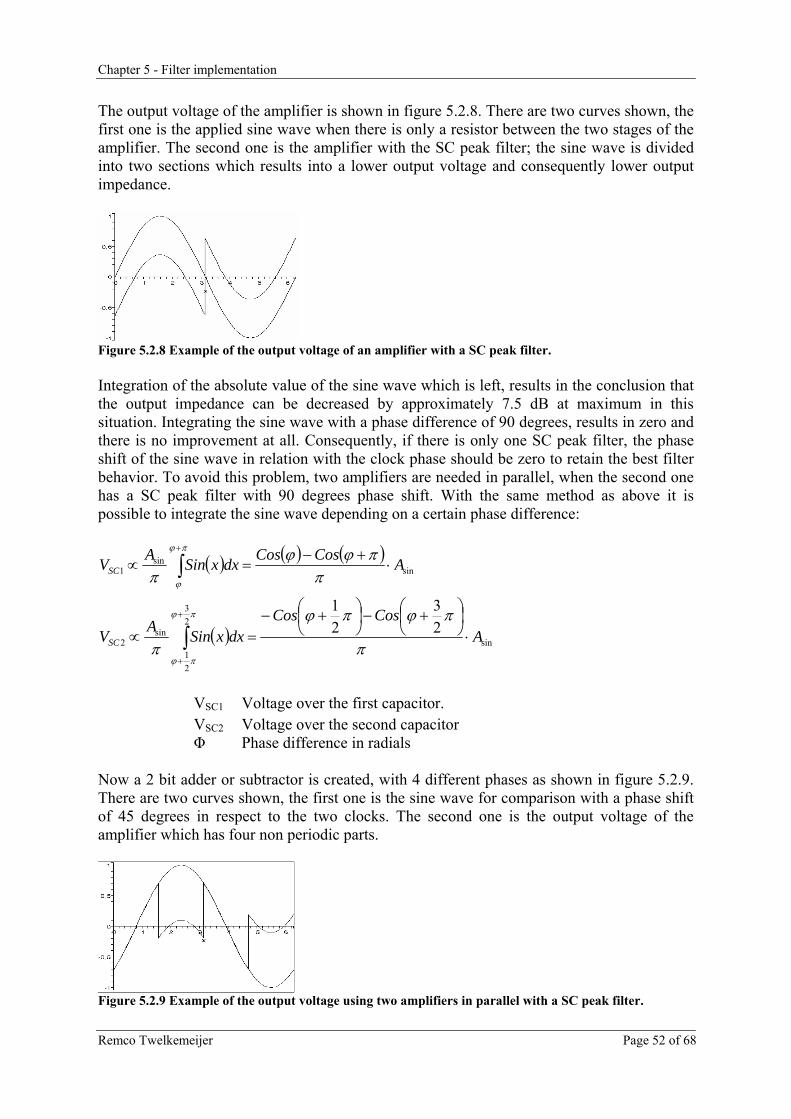
Chapter 5 - Filter implementation
Remco Twelkemeijer Page 52 of 68
The output voltage of the amplifier is shown in figure 5.2.8. There are two curves shown, the first one is the applied sine wave when there is only a resistor between the two stages of the amplifier. The second one is the amplifier with the SC peak filter; the sine wave is divided into two sections which results into a lower output voltage and consequently lower output impedance.
Figure 5.2.8 Example of the output voltage of an amplifier with a SC peak filter. Integration of the absolute value of the sine wave which is left, results in the conclusion that the output impedance can be decreased by approximately 7.5 dB at maximum in this situation. Integrating the sine wave with a phase difference of 90 degrees, results in zero and there is no improvement at all. Consequently, if there is only one SC peak filter, the phase shift of the sine wave in relation with the clock phase should be zero to retain the best filter behavior. To avoid this problem, two amplifiers are needed in parallel, when the second one has a SC peak filter with 90 degrees phase shift. With the same method as above it is possible to integrate the sine wave depending on a certain phase difference:
( ) ( ) ( )
( ) sin
23
21
sin2
sinsin
1
23
21
ACosCos
dxxSinAV
ACosCosdxxSinAV
SC
SC
⋅⎟⎠⎞
⎜⎝⎛ +−⎟
⎠⎞
⎜⎝⎛ +−
=∝
⋅+−
=∝
∫
∫
+
+
+
π
πϕπϕ
π
ππϕϕ
π
πϕ
πϕ
πϕ
ϕ
VSC1 Voltage over the first capacitor. VSC2 Voltage over the second capacitor Φ Phase difference in radials Now a 2 bit adder or subtractor is created, with 4 different phases as shown in figure 5.2.9. There are two curves shown, the first one is the sine wave for comparison with a phase shift of 45 degrees in respect to the two clocks. The second one is the output voltage of the amplifier which has four non periodic parts.
Figure 5.2.9 Example of the output voltage using two amplifiers in parallel with a SC peak filter.

Chapter 5 - Filter implementation
Remco Twelkemeijer Page 53 of 68
With two SC peak filters and a variable phase, the minimum improvement factor is not zero anymore. The improvement factor depends on the phase difference. Integrating the output function depending on the phase shift over the time, the benefit of this filter is calculated and shown is in figure 5.2.10. The phase shift could only difference from 0 to 90 degrees, because the phase of the two peak filters has a phase difference of 90 degrees and more phase difference results in just a minus sign. The maximum benefit is reached at 45 degrees phase difference and is 9dB at maximum. The minimum benefit of the SC peak filter is approximately 7.5 dB, which is the same for only one amplifier with a SC peak filter with a phase shift of zero degrees.
Figure 5.2.10 Improvement when two SC peak filters are set in parallel with 90 degrees phase shift.
5.2.4 Peak filter using eight equal capacitors Extending the peak filter of the previous paragraph with more capacitances, a high Q filter can be created [13, 14]. Now the capacitances are not periodically inverted anymore, but are set in parallel with a switch in series. Only one of the N switches is closed at a time. The proposed filter in [13, 14] is shown in figure 5.2.11 The filter has eight capacitances; this is a trade of between complexities in the control signals versus performance. The quality factor is written in a simplified form as:
OFCRNQ ⋅⋅⋅⋅= π
Figure 5.2.11 High Q peak filter The formula of the quality shows that increasing the capacitance, the resistance and the number of capacitors results in increasing the quality factor. The control signals, x1 to x8 are shown in figure 5.2.12. Only one of the eight signals is ‘one’ at a time. The signal x1 is only ‘one’ between 0 and 0.12 us. A whole cycle of x1 to x8 (To) is equal to the resonance frequency of the filter. In this case, the resonance frequency is set to 1 MHz. The design of the control signals is not described here, but it could be done with a ring oscillator with exclusive or gates.
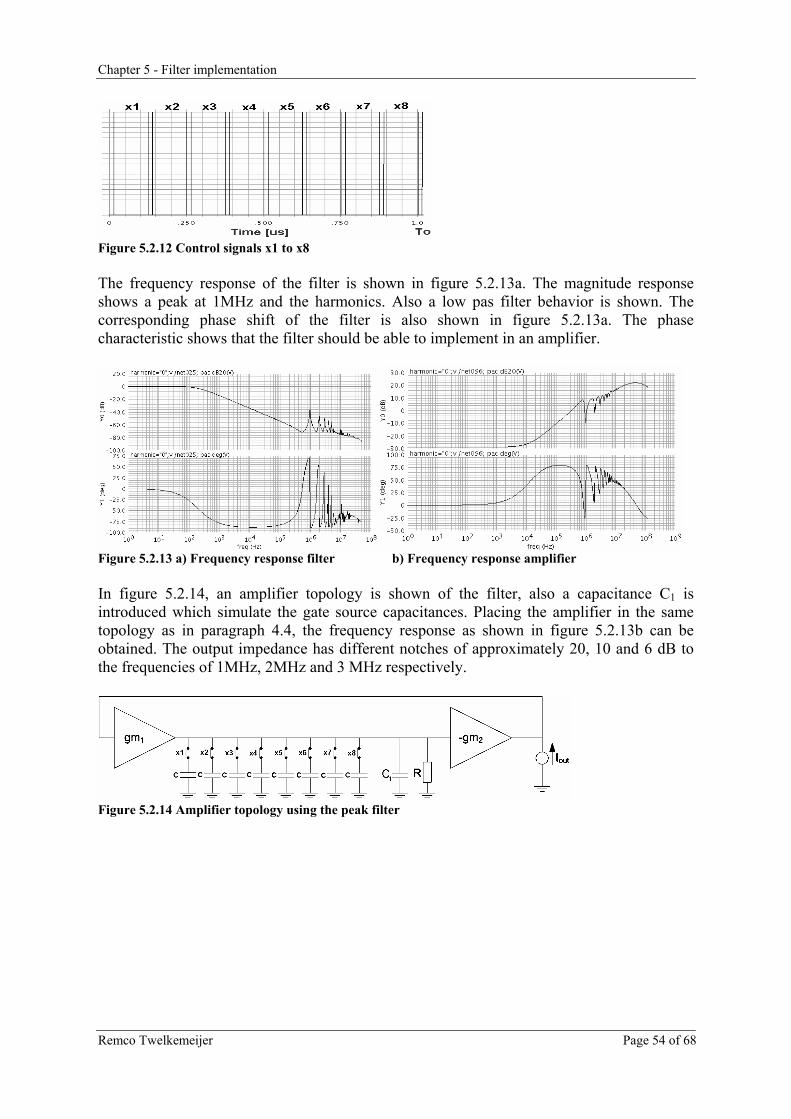
Chapter 5 - Filter implementation
Remco Twelkemeijer Page 54 of 68
Figure 5.2.12 Control signals x1 to x8 The frequency response of the filter is shown in figure 5.2.13a. The magnitude response shows a peak at 1MHz and the harmonics. Also a low pas filter behavior is shown. The corresponding phase shift of the filter is also shown in figure 5.2.13a. The phase characteristic shows that the filter should be able to implement in an amplifier.
Figure 5.2.13 a) Frequency response filter b) Frequency response amplifier In figure 5.2.14, an amplifier topology is shown of the filter, also a capacitance C1 is introduced which simulate the gate source capacitances. Placing the amplifier in the same topology as in paragraph 4.4, the frequency response as shown in figure 5.2.13b can be obtained. The output impedance has different notches of approximately 20, 10 and 6 dB to the frequencies of 1MHz, 2MHz and 3 MHz respectively.
Figure 5.2.14 Amplifier topology using the peak filter

Chapter 6 - Simulations
Remco Twelkemeijer Page 55 of 68
6 Simulations The previous chapters describe the theoretical limitations of the amplifier, some amplifier topologies and methods to implement the filters in an IC process. With these results, simulations can be done with the amplifier in combination with a class D amplifier. First, the amplifier structure used in the simulations is described. There are several filters described in chapter 5 which results in different amplifiers. The amplifiers used in the simulation are described next. With the structure and the amplifiers known, some simulations are done. The results of the simulations are described finally.
6.1 Amplifier structure A simple parallel combination of a class AB and a class D amplifier is shown in the introduction and repeated in figure 6.1.1. The class D amplifier in this structure is defined by the current delivered by the class AB amplifier. This is time independent, the class D switching frequency is variable which could be for example 40 KHz or 1 MHz. The filters which are designed in the previous chapter are not variable. Consequently, the class D amplifier should have a fixed switching frequency to be able to remove the switching ripple. The class AB amplifier should have a voltage source behavior and the class D amplifier should have a current source behavior, because it is difficult to have two voltage sources in parallel.
Figure 6.1.1 Parallel combination of a Class AB and Class D amplifier The switching frequency of the class D amplifier can be fixed if a pulse with modulator (PWM) is used. In a simple version, it is a comparator which compares a square wave with the output current of the class AB amplifier. Also if the output current is higher than the maximum value of the square wave, the class D amplifier should switch to satisfy a constant switching frequency. The class D amplifier is implemented as ideal switches with an inductor at the output to satisfy a current behavior. The linearity or the value of the inductance is not very important, because the accuracy is delivered by the class AB amplifier. The class AB amplifiers used in the simulations are described in the next paragraph. The amplifier structure which will be used in the simulations is shown in figure 6.1.2. The structure contains a PWM, a class AB and class D amplifier, an inductor and a loudspeaker. The switching frequency of the PWM is 1 MHz, the inductance of the inductor (L1) is 0,8mH and the loudspeaker impedance is assumed to be real and the resistance is 4Ω. The threshold of the PWM is set to 95mA. This means, if the amplifier delivers more than 95mA, the on time of the class D amplifier is maximal and satisfying a switching frequency of 1 MHz.
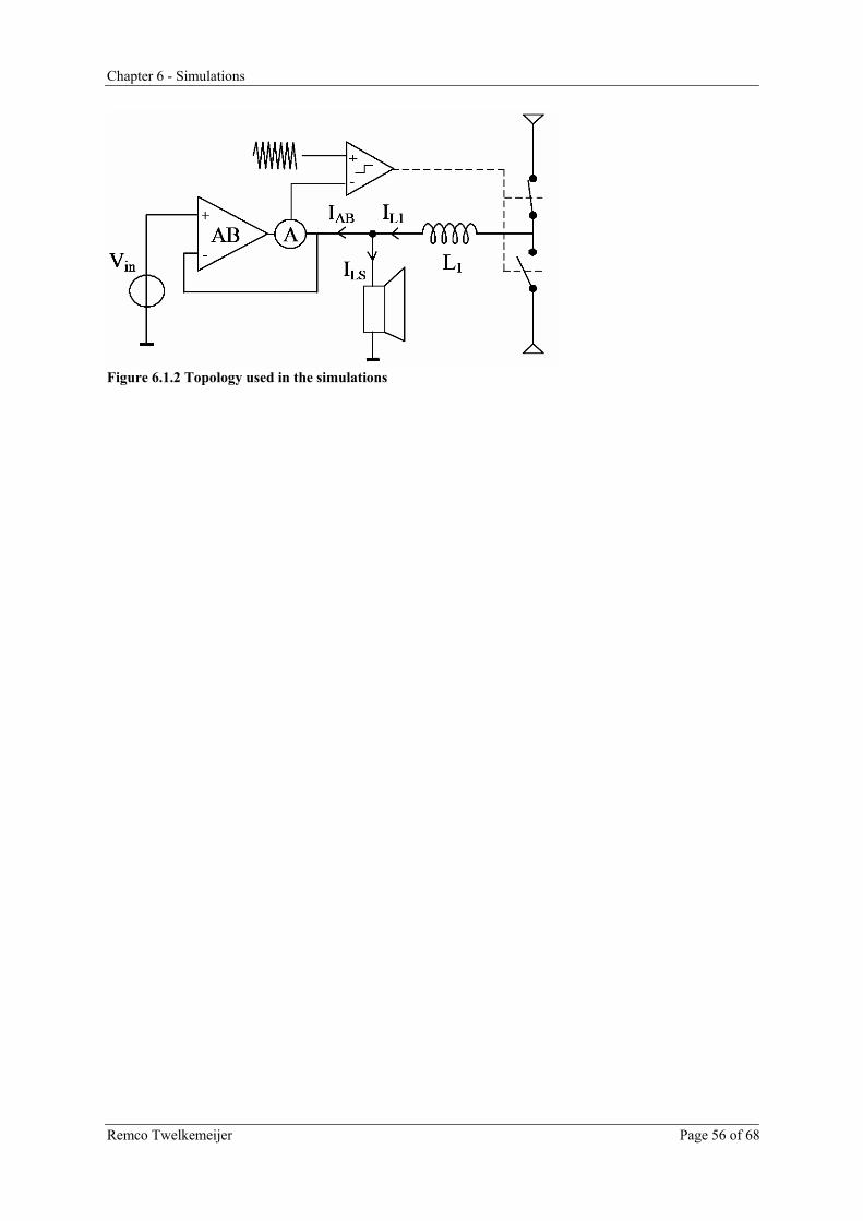
Chapter 6 - Simulations
Remco Twelkemeijer Page 56 of 68
Figure 6.1.2 Topology used in the simulations
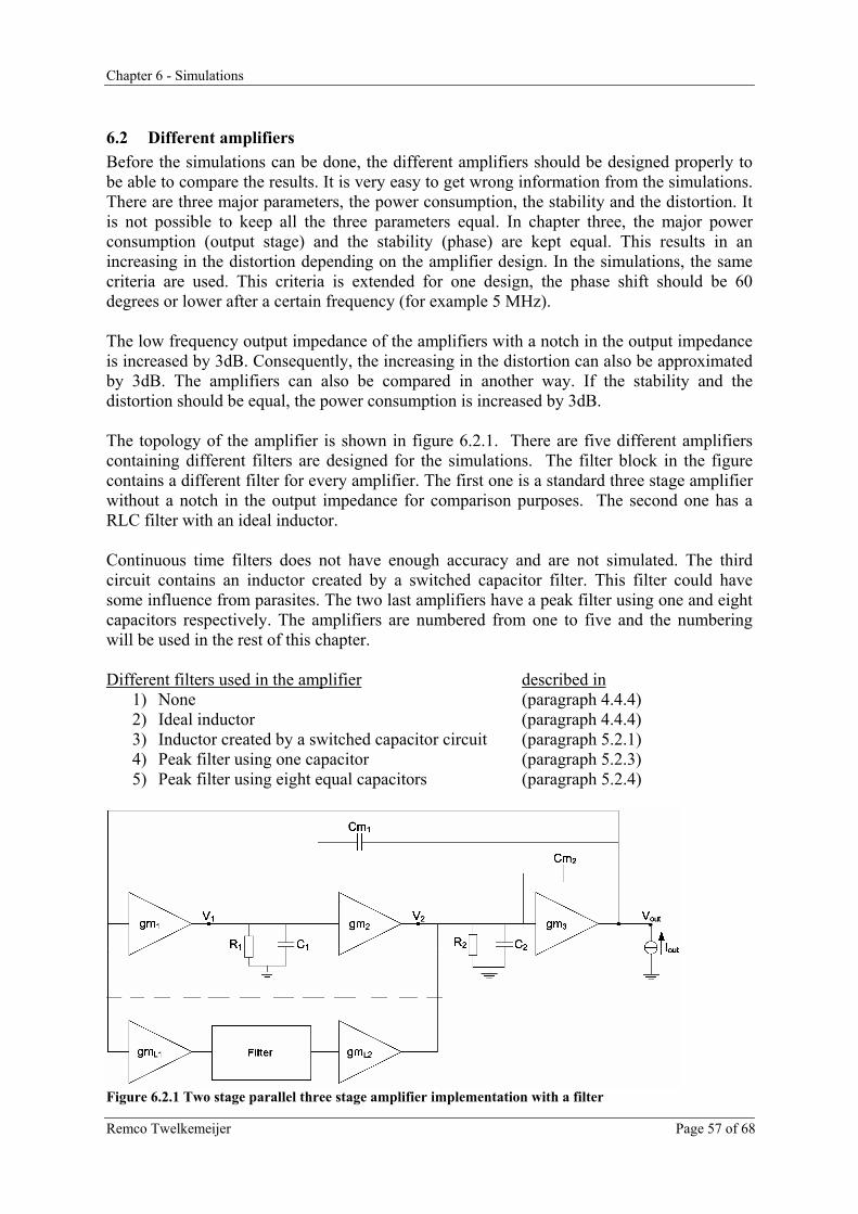
Chapter 6 - Simulations
Remco Twelkemeijer Page 57 of 68
6.2 Different amplifiers Before the simulations can be done, the different amplifiers should be designed properly to be able to compare the results. It is very easy to get wrong information from the simulations. There are three major parameters, the power consumption, the stability and the distortion. It is not possible to keep all the three parameters equal. In chapter three, the major power consumption (output stage) and the stability (phase) are kept equal. This results in an increasing in the distortion depending on the amplifier design. In the simulations, the same criteria are used. This criteria is extended for one design, the phase shift should be 60 degrees or lower after a certain frequency (for example 5 MHz). The low frequency output impedance of the amplifiers with a notch in the output impedance is increased by 3dB. Consequently, the increasing in the distortion can also be approximated by 3dB. The amplifiers can also be compared in another way. If the stability and the distortion should be equal, the power consumption is increased by 3dB. The topology of the amplifier is shown in figure 6.2.1. There are five different amplifiers containing different filters are designed for the simulations. The filter block in the figure contains a different filter for every amplifier. The first one is a standard three stage amplifier without a notch in the output impedance for comparison purposes. The second one has a RLC filter with an ideal inductor. Continuous time filters does not have enough accuracy and are not simulated. The third circuit contains an inductor created by a switched capacitor filter. This filter could have some influence from parasites. The two last amplifiers have a peak filter using one and eight capacitors respectively. The amplifiers are numbered from one to five and the numbering will be used in the rest of this chapter. Different filters used in the amplifier described in
1) None (paragraph 4.4.4) 2) Ideal inductor (paragraph 4.4.4) 3) Inductor created by a switched capacitor circuit (paragraph 5.2.1) 4) Peak filter using one capacitor (paragraph 5.2.3) 5) Peak filter using eight equal capacitors (paragraph 5.2.4)
Figure 6.2.1 Two stage parallel three stage amplifier implementation with a filter

Chapter 6 - Simulations
Remco Twelkemeijer Page 58 of 68
The parameters of the components and filters are given in appendix C. Also the characteristics of the output impedances are shown in the appendix. It shows clearly that the stability and power criteria are satisfied at the cost of an increase of 3 dB in the output impedance for low frequencies. Summarized, the peak of amplifiers 2 and 3 is approximately 10dB, including the loss of 3dB for low frequencies. The notch as an amplitude compared with amplifier 1 of: Amplifier Filter Notch 1 None - 2 Ideal inductor 21 dB @ 1 MHz 3 SC inductor 19 dB @ 1 MHz 4 One capacitor 1 dB @ 1 MHz 5 Eight capacitors 7 dB @ 1 MHz, 6dB @ 2 MHz, 3.5 dB @ 3MHz, 2.3 dB @ 4 MHz, 0.5 dB @ 5 MHz.
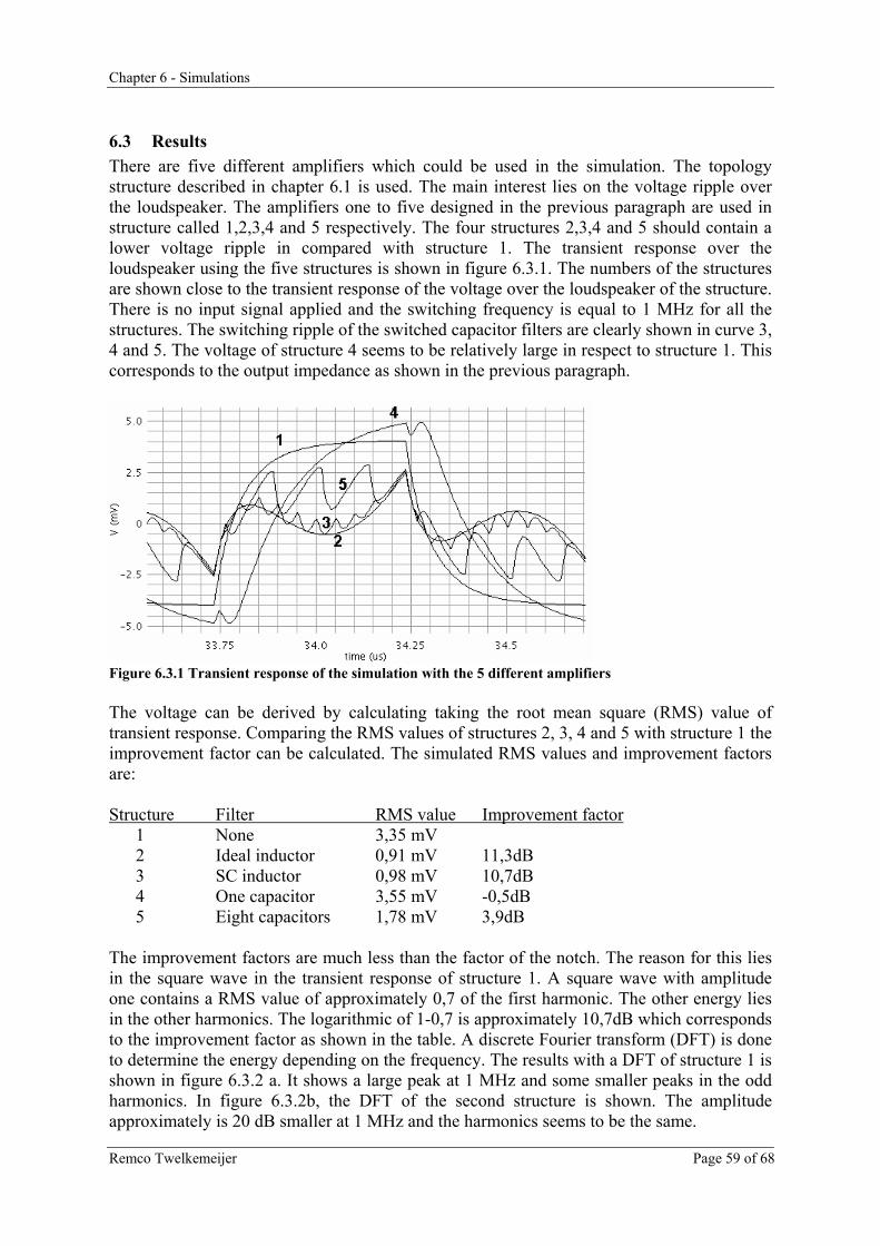
Chapter 6 - Simulations
Remco Twelkemeijer Page 59 of 68
6.3 Results There are five different amplifiers which could be used in the simulation. The topology structure described in chapter 6.1 is used. The main interest lies on the voltage ripple over the loudspeaker. The amplifiers one to five designed in the previous paragraph are used in structure called 1,2,3,4 and 5 respectively. The four structures 2,3,4 and 5 should contain a lower voltage ripple in compared with structure 1. The transient response over the loudspeaker using the five structures is shown in figure 6.3.1. The numbers of the structures are shown close to the transient response of the voltage over the loudspeaker of the structure. There is no input signal applied and the switching frequency is equal to 1 MHz for all the structures. The switching ripple of the switched capacitor filters are clearly shown in curve 3, 4 and 5. The voltage of structure 4 seems to be relatively large in respect to structure 1. This corresponds to the output impedance as shown in the previous paragraph.
Figure 6.3.1 Transient response of the simulation with the 5 different amplifiers The voltage can be derived by calculating taking the root mean square (RMS) value of transient response. Comparing the RMS values of structures 2, 3, 4 and 5 with structure 1 the improvement factor can be calculated. The simulated RMS values and improvement factors are: Structure Filter RMS value Improvement factor 1 None 3,35 mV 2 Ideal inductor 0,91 mV 11,3dB 3 SC inductor 0,98 mV 10,7dB 4 One capacitor 3,55 mV -0,5dB 5 Eight capacitors 1,78 mV 3,9dB The improvement factors are much less than the factor of the notch. The reason for this lies in the square wave in the transient response of structure 1. A square wave with amplitude one contains a RMS value of approximately 0,7 of the first harmonic. The other energy lies in the other harmonics. The logarithmic of 1-0,7 is approximately 10,7dB which corresponds to the improvement factor as shown in the table. A discrete Fourier transform (DFT) is done to determine the energy depending on the frequency. The results with a DFT of structure 1 is shown in figure 6.3.2 a. It shows a large peak at 1 MHz and some smaller peaks in the odd harmonics. In figure 6.3.2b, the DFT of the second structure is shown. The amplitude approximately is 20 dB smaller at 1 MHz and the harmonics seems to be the same.
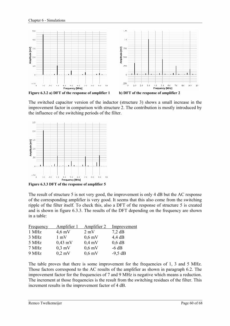
Chapter 6 - Simulations
Remco Twelkemeijer Page 60 of 68
Figure 6.3.2 a) DFT of the response of amplifier 1 b) DFT of the response of amplifier 2 The switched capacitor version of the inductor (structure 3) shows a small increase in the improvement factor in comparison with structure 2. The contribution is mostly introduced by the influence of the switching periods of the filter.
Figure 6.3.3 DFT of the response of amplifier 5 The result of structure 5 is not very good, the improvement is only 4 dB but the AC response of the corresponding amplifier is very good. It seems that this also come from the switching ripple of the filter itself. To check this, also a DFT of the response of structure 5 is created and is shown in figure 6.3.3. The results of the DFT depending on the frequency are shown in a table: Frequency Amplifier 1 Amplifier 2 Improvement 1 MHz 4,6 mV 2 mV 7,2 dB 3 MHz 1 mV 0,6 mV 4,4 dB 5 MHz 0,43 mV 0,4 mV 0,6 dB 7 MHz 0,3 mV 0,6 mV -6 dB 9 MHz 0,2 mV 0,6 mV -9,5 dB The table proves that there is some improvement for the frequencies of 1, 3 and 5 MHz. Those factors correspond to the AC results of the amplifier as shown in paragraph 6.2. The improvement factor for the frequencies of 7 and 9 MHz is negative which means a reduction. The increment at those frequencies is the result from the switching residues of the filter. This increment results in the improvement factor of 4 dB.
Chapter 7 - Conclusion
Remco Twelkemeijer Page 61 of 68
7 Conclusion The output impedance is investigated with a pole zero analysis. This approach shows that a notch in the output impedance results in a higher output impedance for low frequencies. Increasing the output impedance means increasing the distortion. The power in the amplifier should be increased if the same distortion should be reached. Also a peak in the output impedance is introduced, but the peak could be smaller than the notch. The quality factor of the notch should be as large as possible and depends on the accuracy of the filter. With these limitations, an ideal amplifier design is made. This means, ideal components are used, like inductors and transconductances. The first one contains two, two stage amplifiers in parallel. The final topology contains an extra output stage which could be beneficial for the power consumption or large signal behavior. Inductors are not able to implement in an IC process and some filters have been investigated. It is not possible to implement continuous time filters, because they have a very bad accuracy. The accuracy of switched capacitor filters is much better and three amplifiers have been designed. The simulations of the amplifiers in combination with the class D amplifier in parallel shows a decreasing in the output impedance of 11,3dB at the cost of 3dB extra power with the same stability and distortion. This result is obtained by an ideal amplifier with ideal components. The switched capacitor filter contributes some extra distortion by the switching of the capacitances itself. The maximum reached improvement with a amplifier containing a switched capacitor filter is approximately 10,5 dB. This factor corresponds to the expected energy in the first harmonic of a squire wave. A real design of the amplifier will normally results in less improvement. The advantages of removing approximately 11 dB energy of the switching ripple go at the cost of extra energy in the output stage to maintain the same distortion, extra space requirements on the chip by the capacitances and extra amplifier stages in parallel. It is possible to create more notches in the output impedance, but this requires extra power consumption to keep the distortion the same. The benefit of an extra notch is not very large, because most of the energy of a square wave lies in the first harmonic. It seems that the advantage of 11 dB not compensate the disadvantages. Under these conditions, it is not beneficial to design a real amplifier.

Conclusion
Remco Twelkemeijer Page 62 of 68

References
Remco Twelkemeijer Page 63 of 68
References [1] Zee, R.A.R. van der, “High efficiency audio power amps”, Ph.D Thesis, University of Twente, ISBN90-36512875, May 1999. [2] Schaink T., “Output impedance and stability of audio power amplifiers”, MSc. Report, Universiteit of Twente, November 2006. [3] Zee, R.A.R. van der, Heeswijk, R, “Frequency Compensation of an SOI Bipolar-CMOS-DMOS Car Audio PA", van. IEEE International Solid-State Circuits Conference (ISSCC), San Francisco, February 6-8, 2006. ISSCC Digest, pp. 346-347 [4] Hamble A. R., “Electronics”, Prentica-Hall International, Inc., ISBN 0-13-085765-3, 2000 [5] Zee, R.A.R. van der, “Frekwentiecompensatie van CMOS opamps met klasse AB eindtrap onder zware capacitieve en resistieve belasting”, MSc. Report, Universiteit of Twente, June 1994 [6] Mohan P.V.A., “Switched Capacitor Filters : theory, analysis, and design”, Prentice Hall International (UK) Ltd, ISBN 0-13-879818-4, 1995. [7] Theodore D., “Continuous-Time Active Filter Design”, CRC Press LLC, ISBN 0-8493-2573-0, 1999 [8] Razavi B., “Design of Analog CMOS integrated circuits”, Tata McGraw-Hill, Boston, ISBN0-07-238032-2, 2001. [9] Schrage J., “Regeltechniek voor HTO”, HBuitgevers, Baarn, ISBN 90-5574-275-9, 2000. [10] Maruyama Y. et all, Simple CMOS 1/jLω inductive transconductance amplifier, AP-ASIC, 2002. [11] Barthélemy H. and Fillaud M., A CMOS Current-Mode Band-Pass Filter with Small Chip Area, 2002. [12] Burt R. and Zhang J., A Micropower Chopper-Stabilized Operational Amplifier Using a SC Notch Filter With Synchronous Integration Inside the Continuous-Time Signal Path, IEEE Journal of solid-state circuits, vol 41, no 12, December 2006. [13] Paillot J.M. et all, Switched Capacitor Bandpass Filter Tuned by Ring VCO in CMOS 0.35um, IEEE Radio Frequency Integrated Circuits Symposium, 2003 [14] Paillot J.M. et all, Fully Integrated High-Q Switched Capacitor Bandpass filter with Center Frequency and Bandwidth Tuning, IEEE Radio Frequency Integrated Circuits Symposium, 2007

References
Remco Twelkemeijer Page 64 of 68

Appendices A - Derivation of the output impedance
Remco Twelkemeijer Page 65 of 68
Appendices A. Derivation of the output impedance In this appendix, the output impedance of the amplifier as described in chapter 4.2 is derived. During the derivations in this appendix, it is assumed that the miller capacitance will manifest itself at very high frequencies and therefore it is ignored.
Figure A.1 Amplifier with RLC filter
( )[ ] ( )
( )( )
( )( ) ( )( ) ( )
( )( )
( ) ( )
⎟⎟⎠
⎞⎜⎜⎝
⎛+⎟⎟
⎠
⎞⎜⎜⎝
⎛+
+
++⎟⎟
⎠
⎞⎜⎜⎝
⎛+
++
+=
++++++++
==
−−=++++
+⇒+=
+
+=⇒⋅−+⋅=
1
1
1
111
1
1111
2
1
11
2
111
1111111112
12
12
11111112
11111
1
1111111
111
11
//1//
1
m
L
m
L
L
m
m
mout
mL
LLm
out
outout
out
LL
LLRLC
mRLC
moutRLCmoutout
Cgm
sLR
s
CCLR
R
LR
RCCss
CCC
gmZ
sCgmRsLRRRRCmCLsCCLRs
RgmIV
Z
VgmIRRRRCLsCLRs
RsLRCRLRZ
sCZ
sCgmVVZsCVVVgmV
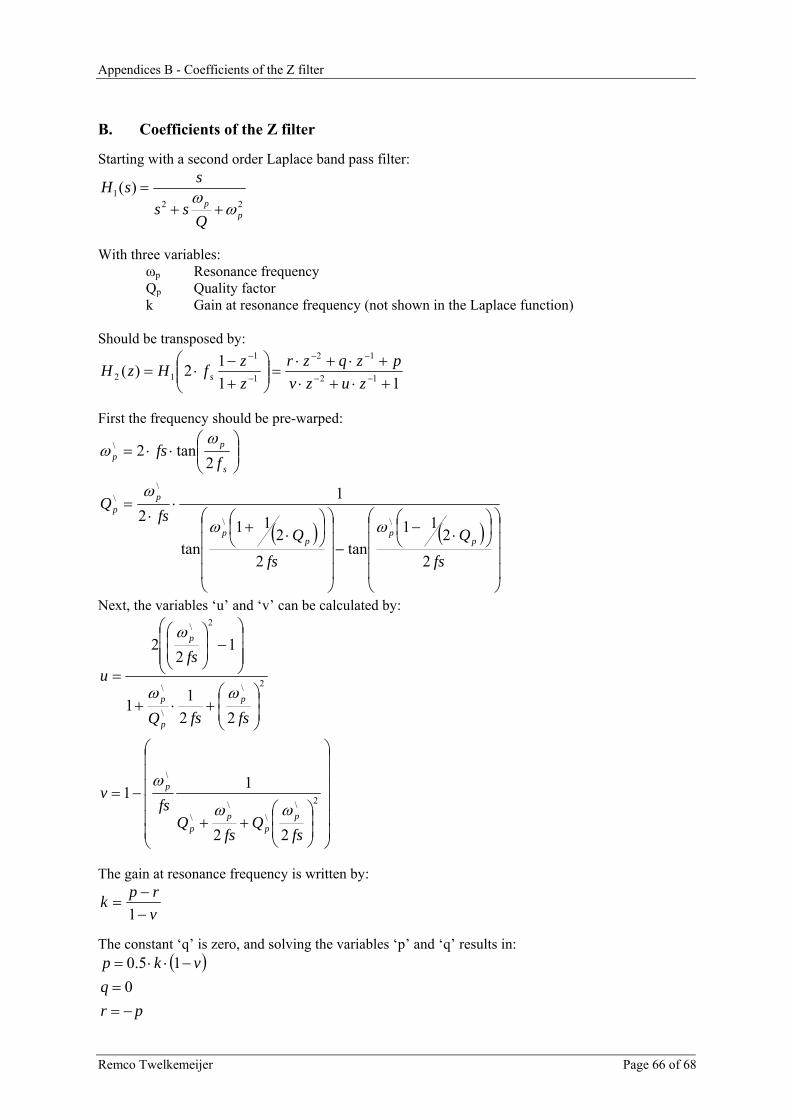
Appendices B - Coefficients of the Z filter
Remco Twelkemeijer Page 66 of 68
B. Coefficients of the Z filter Starting with a second order Laplace band pass filter:
221 )(
pp
Qss
ssHω
ω++
=
With three variables: ωp Resonance frequency
Qp Quality factor k Gain at resonance frequency (not shown in the Laplace function) Should be transposed by:
1112)( 12
12
1
1
12 +⋅+⋅+⋅+⋅
=⎟⎟⎠
⎞⎜⎜⎝
⎛+−
⋅= −−
−−
−
−
zuzvpzqzr
zzfHzH s
First the frequency should be pre-warped:
( ) ( )⎟⎟⎟⎟
⎠
⎞
⎜⎜⎜⎜
⎝
⎛⎟⎠⎞
⎜⎝⎛
⋅−−
⎟⎟⎟⎟
⎠
⎞
⎜⎜⎜⎜
⎝
⎛⎟⎠⎞
⎜⎝⎛
⋅+⋅
⋅=
⎟⎟⎠
⎞⎜⎜⎝
⎛⋅⋅=
fs
Q
fs
Qfs
Q
ffs
pp
pp
pp
s
pp
2
211
tan2
211
tan
12
2tan2
\\
\\
\
ωω
ω
ωω
Next, the variables ‘u’ and ‘v’ can be calculated by:
⎟⎟⎟⎟⎟⎟
⎠
⎞
⎜⎜⎜⎜⎜⎜
⎝
⎛
⎟⎟⎠
⎞⎜⎜⎝
⎛++
−=
⎟⎟⎠
⎞⎜⎜⎝
⎛+⋅+
⎟⎟⎟
⎠
⎞
⎜⎜⎜
⎝
⎛−⎟
⎟⎠
⎞⎜⎜⎝
⎛
=
2\\
\\
\
2\
\
\
2\
22
11
2211
12
2
fsQ
fsQ
fsv
fsfsQ
fsu
pp
pp
p
p
p
p
p
ωω
ω
ωω
ω
The gain at resonance frequency is written by:
vrpk
−−
=1
The constant ‘q’ is zero, and solving the variables ‘p’ and ‘q’ results in:
( )
prq
vkp
−==
−⋅⋅=0
15.0
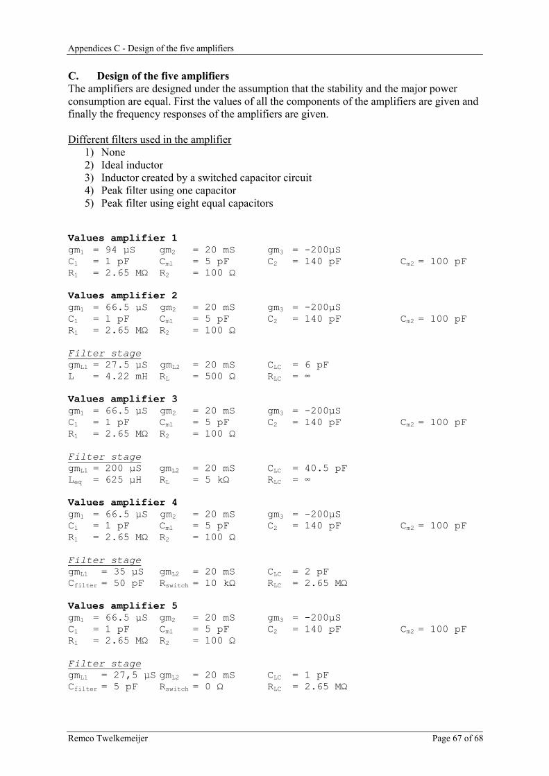
Appendices C - Design of the five amplifiers
Remco Twelkemeijer Page 67 of 68
C. Design of the five amplifiers The amplifiers are designed under the assumption that the stability and the major power consumption are equal. First the values of all the components of the amplifiers are given and finally the frequency responses of the amplifiers are given. Different filters used in the amplifier
1) None 2) Ideal inductor 3) Inductor created by a switched capacitor circuit 4) Peak filter using one capacitor 5) Peak filter using eight equal capacitors
Values amplifier 1 gm1 = 94 μS gm2 = 20 mS gm3 = -200μS C1 = 1 pF Cm1 = 5 pF C2 = 140 pF Cm2 = 100 pF R1 = 2.65 MΩ R2 = 100 Ω Values amplifier 2 gm1 = 66.5 μS gm2 = 20 mS gm3 = -200μS C1 = 1 pF Cm1 = 5 pF C2 = 140 pF Cm2 = 100 pF R1 = 2.65 MΩ R2 = 100 Ω Filter stage gmL1 = 27.5 μS gmL2 = 20 mS CLC = 6 pF L = 4.22 mH RL = 500 Ω RLC = ∞ Values amplifier 3 gm1 = 66.5 μS gm2 = 20 mS gm3 = -200μS C1 = 1 pF Cm1 = 5 pF C2 = 140 pF Cm2 = 100 pF R1 = 2.65 MΩ R2 = 100 Ω Filter stage gmL1 = 200 μS gmL2 = 20 mS CLC = 40.5 pF Leq = 625 μH RL = 5 kΩ RLC = ∞ Values amplifier 4 gm1 = 66.5 μS gm2 = 20 mS gm3 = -200μS C1 = 1 pF Cm1 = 5 pF C2 = 140 pF Cm2 = 100 pF R1 = 2.65 MΩ R2 = 100 Ω Filter stage gmL1 = 35 μS gmL2 = 20 mS CLC = 2 pF Cfilter = 50 pF Rswitch = 10 kΩ RLC = 2.65 MΩ Values amplifier 5 gm1 = 66.5 μS gm2 = 20 mS gm3 = -200μS C1 = 1 pF Cm1 = 5 pF C2 = 140 pF Cm2 = 100 pF R1 = 2.65 MΩ R2 = 100 Ω Filter stage gmL1 = 27,5 μS gmL2 = 20 mS CLC = 1 pF Cfilter = 5 pF Rswitch = 0 Ω RLC = 2.65 MΩ
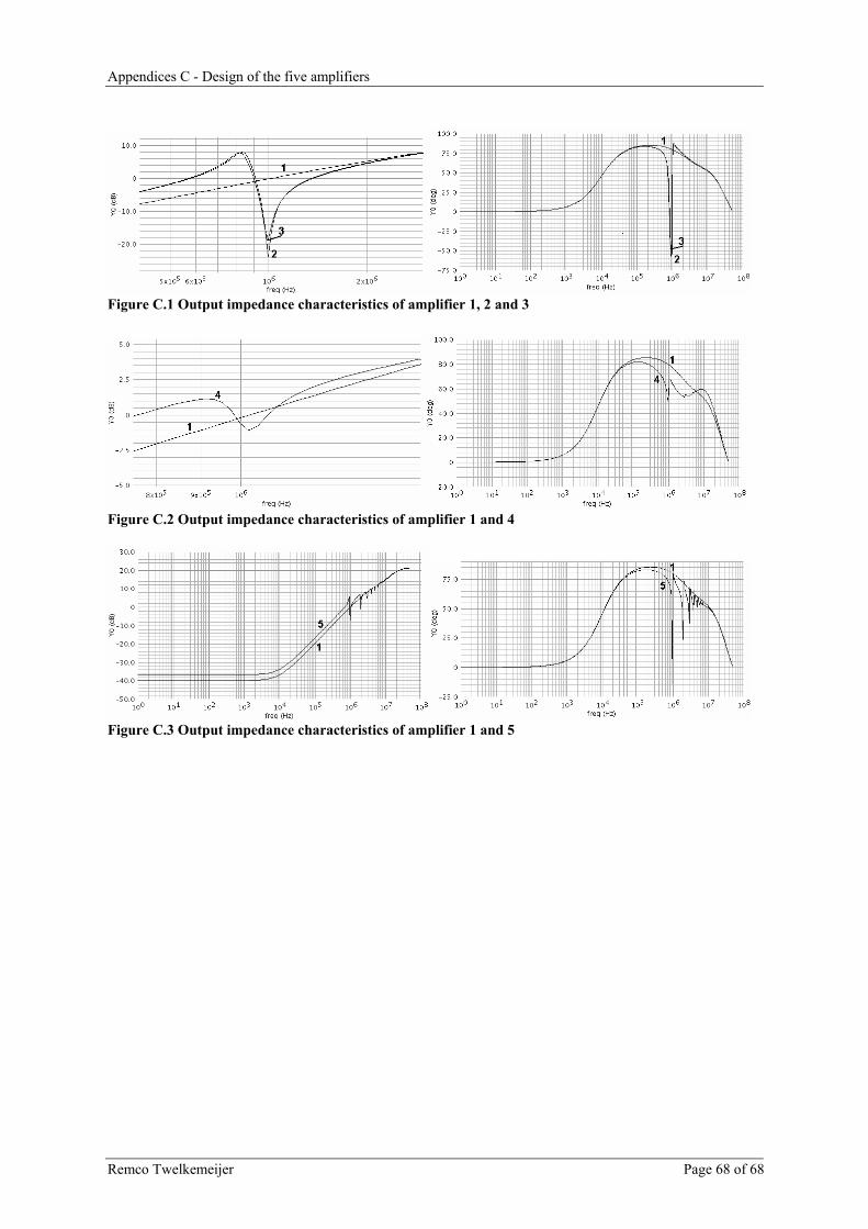
Appendices C - Design of the five amplifiers
Remco Twelkemeijer Page 68 of 68
Figure C.1 Output impedance characteristics of amplifier 1, 2 and 3
Figure C.2 Output impedance characteristics of amplifier 1 and 4
Figure C.3 Output impedance characteristics of amplifier 1 and 5