design, experimentation and fabrication of a low cost ...ic version 4.30 31 tests, precautions and...
TRANSCRIPT

Design, Experimentation and Fabrication of a Low Cost Controller Board for Robotic Applications
by
Rajendra Singh
Submitted to The School of Software Engineering and Data Communications ‘SEDC’, Faculty of Information Technology in partial fulfilment of
the requirements for the degree of
Master of Information Technology
at the
QUEENSLAND UNIVERSITY OF TECHNOLOGY
March 2005
© Queensland University of Technology 2005
Signature of the Author……………………………………………………………….. Rajendra Singh
Certified by …………………………………………………………………………... Dr Fredric Maire
Thesis Supervisor
Certified by …………………………………………………………………………... ASPRO Joaquin Sitte Thesis Co-supervisor
Accepted by…………………………………………………………………………...
Prof Mark Looi HOS-SEDC, FIT, QUT
Accepted by…………………………………………………………………………... Director of Research, FIT, QUT

2
Statement of Original Authorship
The work presented in this thesis has not been previously submitted to meet
requirements for an award at this or any other institution of higher education. To the
best of my knowledge and belief, the thesis contains no material previously published
or written by another person except where due reference is made.
Rajendra Singh Signature …………………………. Date ……………………………….

3
Design, Experimentation and Fabrication of a Low Cost Controller Board for Robotic Applications
by
Rajendra Singh
Submitted to The School of Software Engineering and Data Communications ‘SEDC’, Faculty of Information Technology on March 29th 2005
in partial fulfilment of the requirements for the degree of Master of Information Technology
Abstract This thesis presents the design, construction and experiments done on a micro-
controller board called ‘SMARTY BOARD’ targeted at small mobile robot
applications. The primary motivation for this work was the lack of commercially
available and cheap controller boards that would have all their components including
interfaces on a single board. Having a single board simplifies the construction of
programmable robots that can be used as platforms for teaching and learning robotics.
Reducing the cost of the board as much as possible was one of the main design
objectives. The target user groups for this device are the secondary and tertiary
students, and hobbyists. Previous studies have shown that equipment cost is one of the
major obstacles for teaching robotics in Australia.
The other design objectives were robustness, reliability and functionality of the board.
Most of the early technological learners such as high school students lack experience
and expert knowledge for interfacing a controller board with other components. To
prevent the learners from making errors, connectors on our board have been made
foolproof (the user cannot damage the components of the board by plugging cables in
the wrong sockets). Commercially available designs lack these essential features.
After reviewing the commercially available micro-controller boards with respect to
their suitability as teaching tools, we concluded that none of the existing micro-
controller boards met our requirements. We then designed a new controller board
based on previous boards. The main advantage of this new controller board is that it

4
is a single board whereas the other controller boards are multi-board. Moreover, it is
more foolproof.
The new controller board was demonstrated at high-school seminars. In these
demonstrations the new controller board was used for controlling two robots that we
built. These robots are available as kits. The response from the high school teachers
was very positive. The board has been selected as the platform for a robotic
competition.
Rajendra Singh Faculty of Information Technology Queensland University of Technology

5
Acknowledgments The development of a project is rarely a single person job. A team of people assisted and
helped me at different phases of this project. Dr Alan Tickle had the initial idea of sourcing an
affordable robotic controller for high school teaching. I was just a medium to make it happen.
Dr Frederic Maire and Aspro Joaquin Sitte have always been part of my supervisory team for
most of my technical projects at QUT. They make themselves available to me at very short
notices and so has been the case in this project. I have always enjoyed the freedom to exercise
my casual experimenting ideas with my supervisors. Thanks to Aspro Alan Underwood for
approving the funding of the project and Prof Bill Caelli for giving me the leave from normal
work for a semester so that I could get time to conduct experiments.
This project would not have gone off the ground without the help of the following technical
staff of School of Electrical Engineering of Faculty of Built Environment & Engineering:
Mr. Bob Jenson – Laboratory Manager
Mr. Wolfgang Maier – Senior Technician
Mr. Anthony Tofoni – Senior Technician
Mr. Darren Paul Stacey – Workshop Technician
My sincere appreciation also goes to the management and staff of my previous workplaces.
Thorn EMI Services Australasia, Queensland Deport and NEC Australia, Brisbane office, for
letting me use their facilities and technical resources. I would also like to send my
appreciations to those friends that I have made on line at MIT, Cambridge, MA, USA who
have helped me in doing some of the work that initially I thought were impossible.
Initially, the idea of recycling electronic materials was given to me by two hobbyists whom I
had met in the fall semester in year 2000 at an electronic instrument show in Southern
California. They wish to stay anonymous but I wish to send them my warm appreciation.
I would also like to thank my family for managing the problems I was creating in the house
while working late at nights.
Finally I would like to thank all those persons who have not been mentioned here and have
helped me in some form or another in terms of ideas, thoughts, support and constructive
criticisms.

6
Contents 1 Introduction 9 The Goals of this Thesis 10 Why Teach Robotics in Schools 12 Thesis Contributions 14 Thesis Summary 14 2 Controller Board Designs 16 Controller Board Basics 16 Micro-controller 17 Requirement Specifications 19 EAS Finger Board 20 Allen Systems CP-11 21 MIT’s Handy Board 23 Finalising our Design 25 3 Avenues for Reducing Cost 26 Recycling of Components 26 Other Ways of Reducing Cost 27 Cost of Smarty Board 28 4 Software and Programming 29 The Firmware 29 Interactive C Language 30 IC Version 4.30 31 Tests, Precautions and Errors 32 5 Schematic Design 34 Experimenting for Schematic Design 34 RS232 Circuit 35 CAD Systems Used in Design 39 Finishing Schematic Design 42 6 Prototyping the Board 45 The Prototyping Process 45 Layout and Planning 46 Routing the Tracks and Finishing the Board 49 Testing the Board 50 7 The Main Board Design 55 Cost Reduction Measures 55 Layout of Components 57 Board Routing 58 Final Board 60 8 Experimenting and Testing the Board 62 Smarty-Basic 62 Smarty-Standard 67 9 Discussion and Conclusion 73 Glossary 77 Appendices 78 A. Specifications, Bill of Materials & Manufacturing Constraints. 78 B. Schematics and Artwork 86 C. Smarty Programs 93 D. Smarty Projects: Assembly Materials and Tools 99 Bibliography 110

7
List of Figures Fig 1.1.1 The Smarty-Standard Robot at Work 11 Fig 2.2.1 MC68HC11 series Micro-controller 18 Fig 2.4.1 Finger Board 11 21 Fig 2.5.1 CP-11 Single Board Computer 22 Fig 2.6.1 MIT’s Handy Board 24 Fig 5.2.1 RS232 Circuit 36 Fig 5.2.2 RS232 Board 37 Fig 5.2.3 RS232 Circuit using MAX232 38 Fig 5.3.1 Necessary Fields of a Component 40 Fig 5.3.2 Schematic Symbol 41 Fig 5.3.3 Footprint 42 Fig 5.4.1 Smarty Board Block Diagram 44 Fig 6.2.1 Modified Footprint 47 Fig 6.2.2 Top Overlay Layer of the Smarty Proto Board 48 Fig 6.4.1 Schematic and Built Basic Signal Injector 50 Fig 5.4.3 Basic Logic Probe 51 Fig 6.4.4 Serial Communication Cable 53 Fig 6.4.5 Completed Smarty Proto Board 54 Fig 7.2.1 Component Layout: Smarty Board 58 Fig 7.4.1 Manufactured Bare Board 60 Fig 7.4.2 Completed Smarty-Board 61 Fig 8.2.1 Assembled Smarty-Basic 65 Fig 8.4.1 Maze Test 68 Fig 8.5.2 Assembled Smarty-Standard 70 Fig A.4.1 Bare Small Panel 84 Fig A.4.2 Completed Small Panel 85 Fig B.1.1 Schematic Smarty Board A 87 Fig B.2.1 Schematic Smarty Board B 88 Fig B.3.1 Schematic Handy Board 89 Fig B.4.1 Schematic Finger Board 90 Fig B.5.1 PCB Artwork: Top layer 91 Fig B.5.2 PCB Artwork: Bottom layer 92 Fig D.1.1 Two Gear-headed Motors 100 Fig D.1.2 A Rechargeable Battery 100 Fig D.1.3 Eight 2.5mm X 30mm Machine Screws 101 Fig D.1.4 Suitable Brackets to Mount the Motors and Trailing Wheel 101 Fig D.1.5 Chassis made from Plywood with Holes Drilled 102 Fig D.1.6 Smarty Controller Board 102 Fig D.1.7 Micro-switches as Sensors 103 Fig D.1.8 Wheels cut from Wood 103 Fig D.2.1 Metal prepared Chassis 104 Fig D.2.2 Bumper Bar with four Sensors 104 Fig D.2.3 Wheel Components: Dismantled 105 Fig D.2.4 Wheel Components: Assembled 105 Fig D.2.5 Motors: Gear Headed 106 Fig D.2.6 Motor Mounting Brackets 106 Fig D.2.7 Bracket for Mounting Controller Board 107 Fig D.2.8 9.6V NiMH Rechargeable Battery Pack 107 Fig D.2.9 V IR Sensor for Line Following 108 Fig D.2.A Smarty Controller Board with LCD 108 Fig D.3.1 Tool Kit 109

8
List of Tables Table 2.7.1 Comparison of Features of Reviewed Boards 25 Table 6.4.2 Connectivity of Major Nets (pin numbers on parts) 52 Table 7.3.1 Width and Clearance Constraints for Design Rules 59 Table 8.3.1 Algorithm for Programming Smarty Basic 66 Table 8.5.1 Input Output Connections: Smarty Standard 69 Table 9.0.1 Diversions from Handy Board to Smarty Board 74 Table 9.0.2 Motorola 68HC11 series Micro-Controllers 74 Table 9.0.3 Static RAMs with Identical Packages and Pins 75 Table 9.2.1 Table of Abbreviated and Technical Terms 77 Table A.1.1 Board Specifications 79 Table A.2.1 Bills of Materials of the PCB 81

9
Chapter 1
Introduction It all started in an afternoon in April of year 2000 while I was returning from a visit to
the Central Library of University of California in Berkeley. I was walking with a
friend on University Avenue when we came to an unknown electronic parts shop. I
saw a sign on the window of the shop saying “Motorola on Sale…$1”. We were
curious to know more about the sale. So we went inside and found out that
68HC11A1FN Motorola micro-controller was on sale. I did not know much about this
processing unit then, but since it was cheap I bought five of them. Later when I had
gone through the datasheets of this controller in Motorola manuals, I discovered that it
was more than just a microprocessor. I began experimenting with this controller unit
because it had almost all the components constructed inside the chip for making a
small but complete processing unit. I was not aware at that time that playing with this
micro-controller chip was giving me the knowledge I would require years later to
design a new micro-controller board.
When I was given the task of designing a low cost controller board for teaching
robotics in Queensland high schools, I already knew a component for the board that
was suitable for this application. This controller unit has much functionality all inside
a single chip including analog to digital conversion (ADC). As for most of robotic
applications analog sensors of either infrared or ultra-sonic type are used for distance
sensing, this facility on a chip is critical as it avoids using extra parts. Motorola
68HC11 also has a serial communication interface (SCI) and a serial peripherals
interface (SPI) included. SCI is used to communicate with other devices such as a
computer for downloading programs into the robotic controller (another essential
feature). The other attractive property of the 68HC11 is that it can address up to 64K
locations. This is needed for the applications where external memory has to be large
enough to hold moderate size programs. The most important and attractive feature of
the 68HC11 is its cost.

10
We designed the new board presented in this thesis using this micro-controller and
other parts mostly from recycling of discarded electronic equipment. The boards were
later used together with actuators and sensors (shown in Appendix D) to construct
robots. These robots were demonstrated to teachers and students of Queensland high
schools. The demonstration took place in the year 2004 at a major annual event of
information technology for the schools, the event is known as ‘Share IT’. Share IT for
that year was held at Ferny Grove High School on the 11th of August. Our
presentation was very successful; even the organizers had not anticipated such a large
turnout. Following the presentation, we received many inquiries from teachers
regarding the project. Many were interested in including their schools in our trial pilot
study if we were to conduct one.
1.1 The Goal of the Thesis The goal of this thesis was to design and build a small controller circuit board for
robotic applications. Originally the board was to be used to teach programming of
small robots to students in Queensland high school. During the designing and building
phases we realized that a wider group could be targeted. Undergraduate students and
interested hobbyists in robotics could also be included in the group. We revised our
plan with the following ideas:
• High school students would be given completely built and tested boards. Their
work activities would consist in only assembling robots with these boards. The
students would cut wheels, mount motors/sensors and program the unit.
• Tertiary students (first and second year) may be actually building the controller
boards and experiment with them and test them. Since this project was done at a
university, we found that a huge amount of resources (old computers and other
electronic gear) are always around for recycling. This would be a great learning
experience and also reduce the cost of learning.
• Senior tertiary students could be involved at an advanced level. As in [1] this
board could be modified in a way to suit other types of applications. Most of what
applies to tertiary students also applies to hobbyists
Many existing designs and commercially available products were considered for this
application. None of them actually suited our requirements and hence a new design

11
was required. The construction and maintenance of the board hardware should not
require any special tools or equipment. The interfacing should not call for special
skills so that young learners could use it without causing serious errors and damage.
The new controller board was to satisfy the following requirements;
• The cost of the board had to be as low as practically possible and affordable to the
learners.
• The design of the board had to be simple and robust.
• All the components of the controller had to be centralized on a single board.
• The connectors had to be basic and foolproof when interfacing with other units.
This thesis focuses on the documentation, experimentation, design and the building of
the controller board. The board was named “Smarty Board” when finally completed
and released. The work was taken beyond this point; the completed board was
actually placed on two different models of small robots for thorough testing. The
robots known as “Smarty-Basic” and “Smarty-Standard” were also designed and built
during the course of this project. Documentation related to testing of the board on
these robots is also included in this thesis in Chapter 8.
Fig 1.1.1 The Smarty-Standard Robot at Work The robot follows the edges of a complex shape ‘S’ as the author observes its behaviour.

12
1.2 Why Teach Robotics in Schools We all live in the digital age, no matter what profession one belongs to, he/she has to
deal with electronics and computer technology to some level. Technology is here to
stay. Microelectronics has penetrated into almost all works of life. Researchers such
as Robert Burns had made recommendations about the importance of technology
education mainly electrification in 1995 [2]. Even today our education system rarely
provides appropriate stimulation to universally engage learners with different ability
and motivation into science and technology. So far technological and engineering
subjects are not available in Queensland high schools as major learning units [3].
Some units have the face value of technology but the students are mainly taught how
to use some software applications like MS-Word or MS-Excel [4, 5]. Only a few
schools have introduced programmes in robotics studies. Other countries such as
Israel that have similar size economies as Australia have made technology education
as their main educational framework [6]. We believe that units dealing with
engineering sciences should be made mandatory in middle and senior schools and be
well facilitated through educational authorities. Engineering and technology education
if started in the middle school level could equip learners with the basic understanding
of technology. In senior school, students should be able develop a clear
understanding, for technology is part of the human culture. This is for the young
learners who will have to live with technological culture for the remainder of their
lives in the future work places [2].
We as teachers wish to see that our students are interested and well engaged in their
work. It is not desirable to ‘push’ a learner to make him/her work. When I was a high
school student I had experienced some teachers trying to do their best to make us
learn some technological phenomenon from a book. But hardly anyone took interest
in because the methodology was far too theoretical. Making the topic accessible and
interesting is the hardest part in teaching. The learning processes could be made lot
simpler by introducing engineering subjects through learning about robotics. As
explained by Fred Martin in [7], young students need to be introduced with something
at a level familiar to them in visual terms. Robotic studies can be a very good
introductory subject for a wide range of technological studies. Another work by the

13
same researcher [8] discusses in great depth how technology could be introduced to
young learners in classrooms of elementary and high school learners using robots.
Robotic education offers a wide range of technological experience. By going through
the building and assembling process of robotic hardware, the learners could
experience learning engineering mechanics, technical approximation and manual
skills. Later they will program the unit using a high level programming language; this
will teach them programming and debugging skills. The completion of a robotic
project always fills the students with exhilarating satisfaction. This psychological
reward is also an incentive to continue the technological journey. They are likely to
take up another learning adventure, progressively with less assistance, slowly getting
into managing their own learning as they become adults [9]. Another problem we as
teachers face in the classroom is the problem of behaviour management. Behaviour
problems of learners are very closely related to lack of interest in the learning content
[10]. Robotic studies could arouse that interest and provide a pathway for problem
students to learning progress.
As evidenced by educational initiatives such as Robocup Junior in Australia, at
present the schools that cater robotic studies in Queensland mostly use LEGO RCX
brick as the controller [11]. The brick together with other LEGO blocks does offer
robotic learning for upper elementary and middle school levels. But it does not expose
the technology for upper high school and tertiary learners. We believe that such
learners should actually engage in real technological materials/activities such as
PCBs, hardware fabrication and screws/nuts and not materials that look like toys.
More activities such as Robocup Junior should be organized for upper levels to
encourage higher-level robotic learners and more affordable hardware should be made
available.

14
1.3 Thesis Contributions This thesis makes contributions in the following areas:
• Clear and simple design of a robotic controller board with all the electronics on a
single printed circuit board.
• Exploration of avenues for reducing the cost of board manufacturing through
careful selection of electronic components available in recycled appliances.
• Tutorial on basic electronic tools building for designing and testing.
• Tutorial on ways of building robotic kits with materials easily and readily
available.
• Tutorial on prototyping and debugging techniques.
• The thesis also provides how such a low cost board might be used in schools
1.4 Thesis Summary
The outline of the rest of the thesis is as follows;
• Chapter 2 reviews some previous work on embedded system board designs.
Three boards were taken into consideration for detailed analysis and compared
to decide whether a new micro controller board was needed. This chapter also
explains the role of the controller board in a robotic unit.
• Chapter 3 discusses about cost reducing measures that can be used to make a
controller board more affordable.
• Chapter 4 covers the software and programming part of our project. The
firmware, p-code and programming environment used are covered here as
well.
• Chapter 5 presents the process of schematic design for this project.
• Chapter 6 covers the making and testing of the prototype board. The reason
for prototyping is also explained here.

15
• Chapter 7 explains the cost cutting methods used for making the main board.
The final board planning and routing methodology and purposes are given
here as well.
• Chapter 8 covers the testing of Smarty Board. The making of Smarty-Basic
and Smarty-Standard Robots and testing them using Interactive C programs.
This chapter also provides links to access presentations of video clips of some
demonstrations.
• Chapter 9 provides the conclusion; recommendations and directions for future
modifications on this project have been laid here.
• Appendix A covers the specifications of Smarty Board, bill of materials table
and manufacturing constraints for the main board.
• Appendix B has the schematic diagrams for Smarty Board, Finger Board and
Handy Board.
• Appendix C has the test programs that have been tried on Smarty Robots.
• Appendix D displays the figures of all the components needed to build the
robots mentioned in Chapter 8 together with tools required.

16
Chapter 2
Controller Board Designs In this chapter the requirements specifications of our proposed controller board are
discussed. The modules that make up the board are explained. After reviewing the
basics of micro-controller, we review controller boards that have properties relevant
to our requirements. Many more educational controller boards including Mekatronix
as in [12] were studied that are not described here, only those that were very close to
our design requirements were chosen for review.
2.1 Controller Board Basics
Robotic hardware for educational purposes has to be simple and easy to follow,
especially if it is to be used by early technical learners. Here in this section the
controller board is divided into its four major modules and the purpose of each
module is explained:
• The units that produce (actuate) the outputs such as moving, walking lifting etc. are
called actuators. The wheels or arms that get actuated could also be part of this
module.
• The inputs provide information to the robotic unit to act upon. The inputs can be the
sensors or switches that see or feel the environment of the robot and send
information to it about a job activity or problems.
• The power section provides the energy to the entire unit. It may be a battery in a
mobile robot, associated with a power conditioning, filtering and recharging unit.
There can be more than one power units for a robot, for example one for running the
system processes, one for memory backup and one for supplying the energy to the
actuators.
• The last unit is where all the ‘information processing’ takes place and the decisions
are made. The outputs of this unit are the commands for the actuators. This module
is the brain of the robot, and is called the controller.

17
In larger robotic machines, the electrical/electronics hardware for the modules
mentioned above may be on separate boards. In small robots such as those used for
educational purposes it may not be so. In the modern educational robots such as those
discussed in [13] and [14] most of the stationary parts are centralized to a common
board. The centralized boards are often called the controller boards, embedded
computers or embedded systems controllers. In smaller robots the controller board can
have all the electrical and electronic components associated with the driving of
actuators, processing of sensor information, regulating of power and system processor
circuits. System processor circuits can become very large. In smaller controller
boards, micro-controllers are used to reduce the amount of components for that
section.
2.2 Micro-controller
A micro-controller is actually a microprocessor built together with some memory
devices, signal converters, clock oscillator circuits and more as shown in Fig 2.2.1.
For small applications such as for controlling domestic alarm systems a micro-
controller could be used as a single chip computer with a small amount of associated
components built around it on a board as explained in [15] in Section 2. This could be
the most basic controller board system, but its application would be very limited.
Single chip versions of Motorola 68HC11 controllers are also available in kit format
such as in [16] from general electronics commercial outlets.
A controller board such as that needed for robotics work might not fit in that category.
The controllers needed for robotics work need a much larger memory than that are on
micro-controllers. This is because a robotic system has moderate size software
running on the hardware and all these programs (applications and firmware) have to
reside in the memory. Unlike bigger personal computers these ones do not have
permanent storage devices or discs for saving the software programs.
Apart from MC68HC11 other micro controllers were also considered for this
application. They were versions of Microchip’s PIC and Hitachi H8 series. We did not
get any chance of experimenting with them since they couldn’t be obtained from any
of the sources locally as well as worldwide on line. Though we were successful in

18
tapping some of the vital information such as in [29, 30] to learn about these
controllers.
Fig 2.2.1 MC68HC11 series Micro-controller
The block diagrams of Motorola MC68HC11 series micro-controller such as the one used in our project. The unit has small memory devices built in it so it can be built as a single chip computer with a small amount of parts needed. Source: Motorola [15].
As given in [30] PIC controllers like PIC16F877 has some similar features to
MC68HC11 with extra 256 bytes of flash storage. This flash was too small for our
application. Very little was available for sourcing PIC so we wrote to Microchip’s
Asia-Pacific office in Hong Kong but failed to get a reply within reasonable time. As
information available in [29] H8 (H8/3292) seems to be a suitable unit having similar
resources to MC68HC11 with 16KB of extra ROM. But it is in a surface mount
package not suitable for our application as explained in Chapter 5 of this thesis.
H8/3292 has been used on LEGO RCX in [29] so reusing any part of this design was

19
not possible. We didn’t have much time in hand as we were keen to meet our target
deadline for the purpose explained in Chapter 1 of this thesis. Finally because of a
very narrow and tight resource availability of these controllers we finalised to rely on
MC68HC11 as our favourite micro controller for our board.
2.3 Requirements Specifications
We needed the following facilities in our controller board:
• Power Conditioning Circuit
Our controller board is to take in unregulated power source of 9V-12V, 0.5A-1A such as
those available from general-purpose power packs. All the power conditioning such as
regulation, filtering and noise suppression has to be on board. The board should also be able
to run by these circuits without the battery.
• Battery & Charging
The board will normally run from a 9.6V rechargeable battery both for logic circuits and
actuators energy supply. The board should have all the parts for charging the battery (no extra
board).
• Analog and Digital Inputs
Our new controller board is to have at least eight analog inputs on board for detecting a range
of values from sensors. At least eight digital sensor inputs should be available on board for
simple sensors like micro-switches for limit sensing.
• SCI
Our controller board should be able to communicate with a PC through the communication
ports of the PC for user interaction and downloading of software programs.
• Displays and Feedback
A LCD display on board for user feedbacks and LEDs for conditions (battery charging, reset,
power-on, signal flow for Tx & Rx of SCI and actuator outputs) indicators are needed.
Moreover an audible feedback of multi-tone for signalling alarms and error conditions should
be included.
• Output Drivers
The board should directly drive two small motors (< 7 Watts), two solenoid drivers (< 6
Watts).
• User Control
A switch to turn on/off power supply on board, and keys to start and stop programs.

20
• Memory on Board
Static RAM of at least 32KB with facilities to keep this memory alive, even when power
switch is turned off.
In the following sections three controller boards are discussed. We searched for
designs and architectures that were similar to what we had decided for our design. Our
search was based on facilities available in already tested designs and the electronic
components used for generating those facilities. The boards that are reviewed here
are: EAS Finger board, Allen Systems CP-11 and MIT’s Handy Board. I have chosen
these three because they all use our favourite micro-controller the MC68HC11s.
2.4 EAS Finger Board
There are two versions of the EAS Finger Board manufactured by the Embedded
Acquisition Systems company. We will discuss the most recent version, which is the
second version. It is a micro controller board using Motorola MC68HC11 ‘A’ or ‘E’
chips. This board was designed for running the C compiler/interpreter Interactive C
(discussed in Section 4.2) on small mobile robots like the Rug Warrior robot. Finger
Board can be used for other types of robotic applications as well. This version has two
boards, the processor and the serial communication boards. All the other interfacing
such as sensor inputs and motor driver outputs has to be done through expansion
boards. EAS, the organization that supplies the Finger Board also supplies
information on how to construct the expansion boards. The information is in form of
schematic diagrams and assembly manuals [17].
To make a complete system out of Finger Boards a number of expansion boards may
be needed. How many expansion boards one would need would depend upon the type
of requirements. The main idea of breaking down electronics into many small boards
was for the user to just purchase what is needed for the project, if all was included
into one board a user may have unutilized components on board taking up space and
resources. Embedded Acquisition Systems does not supply all of the expansion
boards. Finger Boards could be purchased either in kit form or fully assembled and
tested. Apart from that, one could also purchase a Finger Board printed circuit board
only and source all the electronic components from elsewhere.

21
Fig 2.4.1 Finger Board 11 Finger Board 11 comes in two parts, the serial communication board and the processor board. They can be easily attached together side by side. The user controls such as manual reset and data load are on the serial communication board. The processor board has all the interface headers for expansion boards including I/O and ADC and more. Source: Embedded Acquisition Systems [17]
Finger Board Specifications:
CPU: Motorola MC68HC11x micro controller running at 8MHz Clock
Memory: Dallas battery backed module 32KByte
Dimensions: 2.00 inches X 4.00 inches
Display: LCD 16 characters X 2lines
I/O: Network capable serial interface,
Expansion ports (8 digital, 8 analog).
Power Requirements: 7V – 18V DC
Suitable Compilers: Interactive C, Small C, ICC11, Sbasic and as11.
2.5 Allen Systems CP-11
The second board that was studied was the CP-11 board from Embedded Products
and Design Services a branch of Allen Systems. This organization designs and
markets many different types of single board computers for embedded system
applications. CP-11 is a much larger board when compared to the Finger Board. It
also had much wider functionalities such as extra 32KBytes of EPROM and an
88c681 DUART chip on board. Through this DUART chip an extra fifteen digital I/O
lines and a serial I/O with RS232 facility are also available. In the fifteen I/O are one
eight-bit output port and a seven-bit input port.

22
Fig 2.5.1 CP-11 Single Board Computer
Apart from I/O, CP-11 does not have any other facilities on the board such as ADC.
For such additional functions, Allen Systems have optional daughter boards. Two of
the common such boards are AC332 and DIGI-DIAC [14]. AC332 is an analog
daughter board providing analog to digital and digital to analog capabilities for many
single board computers. The resources on board include an auto calibrating four
channels, twelve-bit ADC and dual monolithic twelve-bit multiplying DAC. The
ADC chip used on board is an ADS7832BP that has internal sample/hold and 8.5
microsecond conversion time. The DAC chip used on board is a DAC7801LP that is a
dual monolithic CMOS [14]. The board has a very efficient design for low current
consumption. DIGI-DIAC is a motion control daughter board that provides DAC and
Digital I/O capabilities for many single board computers. It has 24 digital I/O and 6
DACs. The chip on board to provide these facilities of Digital I/O is an 82C55 that is
TTL compatible. The DAC is derived from a DAC2815 chip that is 12-bit digital to
analog converter. Just like AC332 this daughter board is a very efficient and
consumes very little power.
Specifications for CP-11:
CPU: Motorola MC68HC11 micro controller running at 8MHz Clock
Memory: 32KByte EPROM & 32KByte SRAM
Dimensions: 3.50 inches X 5.50 inches

23
I/O: 88C681 DUART Chip with 2 Serial and 15 Digital I/O
RS232 buffering on serial A of DUART
8 ADC on MCU
Power Requirements: 5V DC Regulated at 100mA
Suitable Compilers: Interactive C
Other: Supervisory circuit with manual reset.
All CPU lines (Except 2 crystal pins) are brought out to a 50-pin header
2.6 MIT’s Handy Board
Handy Board was designed and built in the mid 1990s by Fred G Martin at the Media
Laboratories of Massachusetts Institute Technology [18]. Professor Martin now with
the University of Massachusetts has been involved with robotic education for all his
life and had made a lot of contributions from elementary schools to tertiary level. His
Handy Board has been very successful; it has been used by universities all over USA
and other parts of the world in wide range of robotic studies [19, 20]. It has been more
than ten years now since its release and it is still very popular. It was fully
documented and released with open source license [21]. The open source licensing
has encouraged people all over the world to use it in whichever way they wished and
the detailed documentation had facilitated the users to understand its design.
Maintenance of Handy board can be very easily done through its documentation and
the most important element is the understanding of its schematic design.
We have used different portions of Handy Board’s schematic to design our controller
board. There are so many attractive features in Handy Board such as I/O and
expansions facilities. All of the I/Os are on the main controller board and it has room
for expansion through expansion headers.
Handy Board is not just used in robotics applications. Educational institutions around
the globe have adopted it to operate for many different applications. At Dartmouth
College, the department of music has been using it in electronic music for MIDI data
processing [20]. This board could be used for multiple applications and this could be
another reasons for the success of this board. Colby Leider of Dartmouth College has
also compiled a wide range of MIDI libraries to be used with Handy Board [22],
which can be freely accessed at http://music.dartmouth.edu/~colby/hb.html.

24
Fig 2.6.1 MIT’s Handy Board
Handy Board version 1.2 was designed in mid 1990s at Media Laboratory of Massachusetts Institute of Technology. It is still
used for educational purposes in USA and abroad. It is available under free licensing.
Specifications
CPU: Motorola 68HC811A1 clocking at 8MHz.
I/O: Inputs- 7 analog, 9 digital
Outputs- 4 actuators
Controls: 2 switches- push button (STOP and START).
Power switch - slide
Feedback: LCD 16 characters X 2 lines
Battery low indicator LED
Power on indicator LED,
Signal Rx LED
Motor Forward/Reverse LEDs
Battery charge indicator LED
Multi tone buzzer
Memory: SRAM 32KB
Power Requirements: 12V DC, 500mA power plug-pack
9.6V rechargeable battery (NiCad or HiMH),

25
2.7 Finalising our Design
Out of all the three boards that were reviewed, Handy Board has most of the features
that we needed on our board to be designed. The only facility that is not on Handy
Board is the RS232 interface; this is on another separate board. Table 2.7.1 displays
the features we needed and features that are available on the reviewed boards. We
chose Handy Board to conduct experiments and testing to begin our controller board
design. Schematics were built through these experiments as explained in Chapter 5
and PCB was built from the schematics as explained in Chapters 6 and 7.
Desired Features Features on Boards Reviewed
EAS Finger Board Allen Systems CP-
11 Handy Board
Power Conditioning Cct (power regulators on board) Regulator on board Not available
2 Regulators on board, one for the memory (un_switched) the other for logic circuits
Battery & Charging (Input: unregulated DC, battery charging cct)
Separate circuit needed Not available
Slow charging available on board. Fast charging through Zap board
Analog Inputs (at least 8 analog inputs)
Port E wired to a header
Port E wired to a header
7 Analog Inputs pulled high ready for sensor connections
Digital Inputs (at least 8 digital inputs) Not available
15 Digital channels through DUART
9 Digital Channels pulled high ready for connections
SCI (RS232 circuit on board)
Available on small board
Available on DUART
Not available on main board, available on Zap Board
Displays and Feedback (a LCD and LEDs for conditions and signal flow feedback)
16 characters X 2 LCD display
16 characters X 2 LCD display
16 characters X 2 LCD display, LED displays for Power/TX, Reset, Motor-forward and reverse.
Output Drivers (2 motor drivers, 2 solenoid drivers) Not available Not available
Motor Controllers on Board – up to 4 DC motors can be driven
User Control Power switch, start key, stop key)
Reset_Button Load_Button Not available
Start_Button Stop_Button
Memory on Board (32KB SRAM)
32K SRAM - battery backed
32K SRAM 32K EPROM
32K SRAM - battery backed
Table 2.7.1 Comparison of Features of Reviewed Boards Handy Board has most of the features when compared to other reviewed boards. CP-11 also has many attractive features but it comes at an expense of a DUART chip, not desired for our low coast design.

26
Chapter 3
Avenues for Reducing Cost
This chapter surveys some cost reduction methods used for obtaining electronic parts.
The electronic parts are one of the important elements that makeup the cost of a
board. A controller board is a small computer with almost all its associated parts
centralized closely into either a single board or into several smaller boards, as seen in
Chapter 2. Computers of this type normally have a common selection of electronic
components. This includes a microprocessor or a micro-controller, some memory
units, communication units and motor controller units. To interface these main units
some additional components such as associated logic circuits, discrete and passive
components are also needed. Most of these major units are expensive to obtain and it
is difficult to find the required type. One of the options for cost cutting is to recycle
electronic components as explained in section 3.1. The other option for making
electronics affordable is to use older micro-controllers and memory devices that are
very cheap and readily available.
3.1 Recycling of Components
Electronic components can be taken out of equipment that is not needed any more and
the components can be reused. Many organizations write-off old electronic gear and
nearly all of useful electronic materials normally end up at the tip or in landfills. A lot
of these could be recycled and electronic parts extracted for reuse. These include old
computer boards and domestic electronic gear such as stereos, television circuit
boards and radios. A lot of logic gates could be unplugged from sockets of computer
boards and be reused. The main advantage of such a process is the cost of the parts is
almost nothing, since people discarding them actually will be happy for someone to
collect and take it away. The only change from the standard procedure of designing is
that the design process has to be based on the components already in hand. In a
standard case of electronic designs desired functions are decided first and then
suitable parts are sourced. Older computer boards have a lot of electronic parts
available on them that could be fit in a controller board. One of such parts is the static

27
RAM used as cache RAM on 386 and 486 and earlier Pentium mother boards. These
SRAMs are normally of 256 kilobits organized as 32K 8bit words which is a suitable
property for standard designing. They are also in DIP standard or skinny 28pin chips
packages normally plugged on IC sockets on main boards. They could be easily
unplugged and reused without the need for complex de-soldering. Apart from RAMs
many 74xx series logic circuits are also available on these boards.
At Queensland University of Technology we found that there was a lot of electronic
gear getting written off every season. We arranged a method of collecting them and
taking out whatever parts that could be reused. We had examined a lot of older
electronic boards and began collecting parts. We were surprised with our collection;
in a period of a fortnight we had collected over 900 pieces of static RAM that were
used as cache. Over 1000 pieces of logic gates and about 2000 pieces of tri-colour and
single colour Light Emitting Diodes. We had also collected a lot of hardware such as
several large containers full of IC sockets, screws, nuts gears motors and much more.
This gave us a very clear picture of this new ‘power of recycling’ as applied to
research and development. We came to know this method of parts collection through
experimenters/hobbyist in California, USA.
3.2 Other Ways of Reducing Cost
One of the other means of bringing the cost down of a project is to use components
that are cheap. The prices can vary in a wide range when shopping for electronic
components as we found out through our research. We began searching on electronic
materials locally as well as globally through the web. Though we found so many
micro-controllers that could be employed in our project, our favourite remains the
Motorola 68HC11 for two reasons. One of the reasons is its functionality the other is
its price. The A1 version (MC68HC11A1) was available for $US5.99 at Mr. Robot an
online store: http://www.mrrobot.com. That was its normal price with them, in fact
when on special it is reduced to $1.00. To compare we had another supplier in
Australia who quoted us $A52.50 for the same unit. This controller comes in two
different packages, 48pin DIL and 52pin PLCC. The DIL package has reduced
functionalities and is normally cheaper, but here Mr. Robot was selling the PLCC
package at that price. As mentioned earlier in Chapter 1, I had purchased this

28
controller unit for the same price at another outlet in Berkeley, California and there
could be more places to buy it from. This makes the MC68HC11 very suitable for our
low cost project.
Another method of reducing costs was to use components that are easily available.
This method does not just reduce the cost during initial construction and design but
also makes it cheaper during the maintenance processes. Some technologists with
whom I had discussed about project maintenance regard electronic units as those that
fail very easily and require a lot of spares and repairs to stay in working condition.
This means we also need the parts even after initial construction and we should get
them quickly, so that there is a maximum utilization of the unit. These days due to the
miniaturization push a lot of parts are normally integrated together in a single
package. This is good for mechanized assembly in mass production but if one of the
units malfunctions or fails during operation, the whole package unit has to be replaced
and that increases the cost. Because of this factor we had plans of not using such
packages. One of those packages are resistor packs, we planned only those resistor
packs that were easily available and to use standard single resistors for the majority of
cases in our project.
3.3 Cost of Smarty Board
By using our cost reduction methods we are able to produce a Smarty Board for about
$A30. The major cost cutting element is recycling but the PCB design (explained in
Chapter 7) also plays a significant role. Please note that this is a ‘Do It Yourself” type
of project activity. All the tasks of removing the parts from older PCs, testing the parts
and assembling of the Smarty Board is not included in the cost. Also older unwanted
PCs are collected at no cost to us. If we were to outsource the assembling of the board
(new components, no recycling), the total price for an assembled Smarty Board would
be about $A197. The cost of the PCB only of the Smarty Board is below $A10
(provided we order more than 1200 boards) due to our cost cutting design methods.
Detailed cost figures are given in Table A.2.1 of Appendix A.

29
Chapter 4
Software and Programming This chapter deals with the software of the embedded controller board. In Motorola
systems, a firmware known as ‘S19’ file gets first loaded in the memory of the
controller and then the user programs are downloaded. The firmware is discussed in
Sections 4.1. The applications that run on the host computer for interacting and
downloading of the programs on the controller board are discussed in Sections 4.2 and
4.3 of this chapter. The application IC 2.8 is a DOS based interactive ‘C’ language
initially used with MIT robotic platforms. IC 4.30 is an interactive C application from
KISS Institute for Practical Robotics. IC 4.30 is intended to be used with a wide range
of robotic applications and is available for free on the web for educational purposes at
http://www.botball.org. We have used IC 4.30 in our robotics project.
4.1 The Firmware
The embedded system computers operate in a slightly different way than standard
personal computers. A program known as firmware gets first started on the embedded
machine to make the unit ready for utilizing all the other hardware or devices
connected around the micro controller. In electronics the devices are known by their
address of connection, a library file with a particular compiler would also be needed
to translate the physical address values to some logical names. For example a call
such as “motor(1,50)” is a call with Interactive C for switching on a motor connected
to motor 1 port at a speed of 50% of the maximum. The compiler will translate such a
call and pass the raw information to the hardware. Sometimes this raw information is
tapped and read in binary or in HEX format for debugging the hardware/software
problems. In the embedded system the software code is normally written, checked and
tested on a PC first and then downloaded onto the system where the firmware is
already running. Since the firmware is the software component that brings an
embedded computer alive, problem arises as to how to load the firmware software
onto the embedded system computer, for it is not alive at that stage. Micro-controllers
have different modes of operation, and one of those is this firmware-loading mode. In
Motorola systems it is known as bootstrap mode where the micro-controller gets
30
ready to receive data on its serial communication channel and storing it at a particular
location of the memory. As soon as the load of firmware completes the system can be
reset so that it can “boot” on the loaded firmware. The rest of the software can be
loaded after the booting process completes. At times these firmware programs on
Motorola systems are called S19 files since these files have the extension as
“filename.S19”. Another commonly used name for firmware is ‘p-code’. Two of the
common firmware files for Motorola are listed below:
• For using on Rug warrior platform on Motorola 68HC11 system on a controller
such as a Finger Board written by Randy Sargent of Media Laboratories, MIT:
Pcode_RW.S19.
• For Handy Board or similar system the firmware written by Fred G. Martin and
Randy Sargent of Media Laboratories, MIT: Pcode_HB.S19.
4.2 Interactive C Language
Interactive C (IC) is a simplified C language compiler and a run-time machine
language interpreter together in one module. The compiler can run interactive
command-line compilation and debugging. Just like ANSI C, IC implements control
structures (for, while, if, else), local and global variables, arrays, pointers and
structures. It also supports 16-bit and 32-bit integers, and 32-bit floating-point
numbers. IC can be used with different hardware-processors because it does not
compile directly into native code for a particular processor. It compiles into pseudo-
code for a custom stack machine and the run-time machine language program then
interprets this pseudo-code. Writing a compiler in this format is a lot easier than
writing compiler for a typical processor [23] since the pseudo-code is machine
dependent, using the compiler with another processor does not need any change in it,
only change needed is in the interpretation. The interpretation here takes place during
run time and this also protects against some programming errors [23]. There are many
other advantages as well. The resulting object code is much smaller for the stack
machine when comparing with native code representation. Since it is stack based, the
process’s state is fully dependent on the stack and the program counter and hence it

31
can offer multitasking. In a case such as small single board computing where the
clocking speed is only a few megahertz execution speed is important. IC offers that,
through this unusual design [23].
Professor Fred Martin of Massachusetts Institute of Technology initially wrote IC.
Version 2.8 was released with Handy Board 1.2. In this version the interaction from
the user on the host PC to the embedded computer was similar to command line
interface, the interactive session started after loading of the firmware. This version of
IC had a separate downloader that was used to download firmware and programs in
the memory of the controller boards.
4.3 IC Version 4.30
The present version of IC is IC 4.30, written by Randy Sargent and Mark Sherman of
the KISS Institute for Practical Robotics. Portions of the code and the libraries are
based on the earlier public distribution of IC 2.8 written by Fred Martin. This new
version not only works for handy Board but also for Lego RCX. When IC is running
and has a connection to a compatible processor board such as the Handy Board or
RCX, C expressions, function calls, and IC commands may be typed in the command
entry portion of the interaction window. When this expression is entered from the
interaction window, it is compiled by the console computer and then downloaded to
the attached system for evaluation. The connected board then evaluates the compiled
form and returns the result, which is printed on the display section of console
interaction window. To evaluate a series of expressions, create a C block by beginning
with an open curly brace ‘{‘ and ending with a close curly brace ‘}’.
Apart from the interaction window IC 4.3 also has a file open window. This window
is a text file editor. Here an already written C file can be opened, edited or created for
downloading on the processor board. When the file is saved the file will have a
default ".ic" extension but could be changed to “c” extension. To download the active
file, simply click the download button. The remaining tool bar operations are common
to other windowing application facilities such as saving a file, creating a new file or
editing a file. In some ways IC is different from C for there is no need for importing
libraries with #include statement as in standard C. As with IC 4.3 the library gets

32
loaded just after loading of firmware as a single batch. The library will be available to
the programs without any include statement. Apart from this difference the remaining
programming parts of syntax, control flow and ending could be regarded as standard
C.
Though the IC language is somewhat based on ANSI C, there are significant
differences. The authors of IC have claimed that these distinctions are to make IC
safer than standard C [23]. The other reason is to make IC smaller, simpler and
efficient so that it could be loaded on smaller boards where the resources are not as
much. For more details of IC and the full set of functions please refer to IC
Programmers Manual in [23]. The entire library functions for using it on a RCX or on
a Handy Board are very clearly explained in this manual.
4.4 Tests, Precautions and Errors
Precaution about IC 4.3 when using pointers in a program: If a program is written and
then loaded on the memory of a controller and if that program did not perform what it
was intended to do, it may corrupt the firmware. In such a case the firmware has to be
reloaded. In IC 4.3 there is an option for downloading the firmware at any time under
the settings toolbar. When writing a program in IC window there is a facility for
checking for errors. Though the check only is limited to syntax errors. But this tool is
very useful, in case of errors the line numbers where the errors are get reported, the
edit button provides a go-to line option. Note this is an approximate reporting; the
error may be on that line or in nearby lines. There is a feature in IC 4.3 for
automatically formatting the written program and this formatting option is turned on
as a default when it is installed, it can be turned off if required. If this facility is on, it
formats keywords, library functions, text strings inside “” and comments as highlights
in different colours. IC also supports parenthesis-balance-highlighting. When the
cursor is placed to the right of any right parenthesis, bracket, or brace its matching
pair gets highlighted.
For the testing process of a board, some test functions can be written in a program and
the program can be downloaded on the board. Each of these functions could be called
for running the test from the IC interaction console in IC window on the PC. We

33
found this facility really important when we used IC in our testing of the board. For
those who are familiar with C the next two cases of information are very important.
Unlike C in IC the function “main()” is the function that starts automatically when the
board is reset and the function “printf()” displays the text on the boards LCD screen.
To make it clear, these functions are not intended to show any activity on the PC’s
screen but on the controller board’s LCD screen. We found this very handy; to
automatically start an activity on a robot when switched on and activity responses get
displayed on the screen during trial of a program.

34
Chapter 5
Schematic Design The schematic design of Smarty Board has been inspired largely by the Handy Board
with modifications to suit our requirements. In this chapter the practice of schematic
design of our board is explained. It was desired that all the electronics of the
controller onto a single board. Also most of the components for the board were to be
the ones we had obtained from our recycling cost reduction method. The schematic
was designed using a CAD system where the net data could be ported over from
Schematic to PCB mainly for the physical connectivity of the nets. The entire
schematic was based on components with footprints of ‘hole-through’ type. The main
reason for avoiding ‘surface-mount’ components was simpler board construction and
easier maintenance.
5.1 Experimenting for Schematic Design
We could not find a design that could meet all our requirements. The design that came
closest was the Handy Board though the other models that were studied gave us
plenty of ideas. Handy Board was the best design that we came across, it had many
features that we needed and over all it has been tested and proved to be one of the top
robotic controllers over many years. In short Handy Board had almost all the facilities
that we needed, but the properties that we needed to look at or modify were:
• It came with at least two boards for covering most of our requirements but we
wanted a single board.
• It had been designed with an expensive memory chip and not readily available, we
were to use our memory chips collected from recycled boards.
• It had an RS232 converter chip but on a separate board, we needed to build it on
our main board.
• It had resistor packs used for all pull-up, voltage dividing and biasing, many
values were not common ones and almost impossible to source. We were to use
single resistors for most of the applications and only use commonly available
resistor packs.

35
We came to the conclusion that we should use Handy Board to start our pilot
experiments and build our design from there. We purchased a Handy Board’s main
PCB from Mr. Robot, the online store on the web to begin our project
experimentation. We did not purchase the second board for we had a plan to work out
things differently as explained later in section 5.2 of this chapter. Most of the
electronic components that were needed we had collected through recycling and there
were just few odd ones to be purchased. We had the micro-controller that I had
purchased in Berkeley and a lot of other hardware was in our toolbox. Handy Board’s
main board had most of the components on it for experiments except the SCI voltage
level converter. The SCI converter was on another board together with the power and
high charging unit. The two boards get connected together by RJ11 connectors on
both sides. Finally this second board gets connected to the host computer by a DB25
connector to the serial communications port of the host PC. That meant the RJ11
connectors brought in the send and receive lines of the SCI well as the unregulated
power to the Handy Board. The name given to this second separate interface board by
Professor Martin was Zap Board.
Assembling the Handy Board was simple and clear. Professor Fred Martin in [13]
very clearly explains step by step how to go about assembling and testing the board at
every step. Moreover if the testing does not produce the required result; he also
provided debugging procedures. We did not have many problems; in fact we were
going in a ‘slow motion’ for I had two more students assisting me, and they were
learners learning about electronic assembly at the same time. They were getting first
hand visual information about working on practical electronics. As in [24], students
find it much easier to capture ideas by actually viewing the practical processes of
work. The moment we were placing components on the board, we were also gathering
information on the changes that we were to make when designing our project. The
board was finally ready for programming in about 2 days.
5.2 RS232 Circuit
The Zap board of the Handy Board was to be done before the main board. This is
because each step of the testing of Handy Board required communication with the
host computer. As we did not purchase the Zap board but made our own small board

36
with RS232 level conversion using discrete components to satisfy the SCI
requirements by the main Handy Board. The design experience we had in
microelectronics was really helping us here at that stage. We came up with a simple
but working circuit that used some of the resources from the signal being sent to it.
The schematic of our circuit is shown in Fig 5.2.1 and the actual assembled unit is
displayed in Fig 5.2.2
Fig 5.2.1 RS232 Circuit This circuit uses discrete electronic components to perform RS232 voltage level conversion. The Embedded system computer boards have signal levels from 0V to 5V for logic 0 to 1 but PC’s serial communication has –12V for logic 0 and +12V for logic 1. A circuit such as this would be needed to interface embedded systems to PCs.
The circuit in Fig 5.2.1 does not generate any of the +12V and –12V as is normally
done in specially designed RS232 chips. Integrated circuits such as MAX232 from
Maxim generate those voltages in them together with some external capacitors [18].
We thought to use the incoming signal of –12V from the host PC and store it in a
capacitor C1 and reuse it as our –12V when sending the negative signal to the PC.
Initially we had a normal diode in place of L1 for rectification but later we replaced it
with a LED so that it serves two purposes, rectification as well as indication display
for the signal arriving from the PC. The application software Interactive C that is used
by Handy Board as the working platform needs this signal indication [18]. As for
+12V supply, we did not find it was necessary in our case. We found that the signal
sent to the host as +5V registers as logic high anywhere so we thought to keep it

37
simple. Our circuit worked without any hitches. We did not design a printed circuit
board for our RS232 circuit, we found the circuit was too small and could be made on
a Vero-board with 0.1inch grid holes. The completed board is shown in Fig 5.2.2. We
found that the generic Vero-boards are very handy for quick construction of circuits
during experimentation. Finally the connecting plugs and wires were placed into the
board, a DB9 for connection to the PC and an RJ11 to the Handy board. This circuit
construction not only removes the requirement of the separate Zap board, but also is
used in the main schematic design of Smarty Board.
Fig 5.2.2 RS232 Board The small circuit constructed on Vero-board. It uses 2 transistors, 5 resistors, a capacitor and a LED for circuit operation. A small 5V regulator was also needed for the +5V supply to circuit since the voltage that came through Handy Boards RJ11 connector was direct battery supply of 9.6V.
To compare the performance of our RS232 board with the performance of a specially
designed integrated circuit for that type of work, we also had constructed a similar
board using Maxim’s MAX232 IC. This IC requires four external capacitors as part of
the voltage conversion processes. The completed Maxim board is shown in Fig 5.2.3.
As we understand the two circuits operate differently but we found no difference in

38
performance when tested with Handy Board. Removing the necessity of an additional
communication board such as the Zap Board was our first modification. As Handy
Board’s has low charging circuit together with main power supply on Main Board we
were quite comfortable with that so we did not need a fast charger for experiments.
Fig 5.2.3 RS232 Circuit using MAX232 Maxim’s MAX232 requires additional electrolytic capacitors as seen on this board. To regulate the supply a 78L05 voltage regulator was also needed. This unit was needed to compare the results with the results of our RS232 board.
When finally experimenting with Handy Board we found that this board had all the
programming and I/O facilities. Also the display system used was good enough for
programming and debugging. However we had some problems that we needed to
address, they were as follows:
• As mentioned earlier we needed to put the entire electronics on to a single board.
The schematic design of Handy Board did not decouple the power supply rails at
every active component so in our case we placed a 0.1uF capacitor across the +5V
and ground pins of every integrated circuit.
• During our testing we had connected a variety of small motors to be driven by the
board’s motor controllers. We found that the programs froze when driving some
motors, especially when switching them either ON or OFF by the programs. We
had tried many modifications and found that placing capacitors across motor

39
supply and motor ground and also across logic supply and motor ground of motor
controller chips solved the problem. The theoretical ideas of noise reduction
described in electronic textbooks that are normally overlooked during practical
work, these ideas were finally employed here as a remedy.
5.3 CAD Systems Used in Electronic Design
In the early days of electronics, the schematics and printed circuit boards were
designed manually on a drawing table. Circuit connections from schematic to printed
circuit were to be transferred manually and so were all the properties of components
like component ID and footprints. That was a very difficult process and was never
free from errors. Especially when a circuit contains thousands of components, and
many of the components have a large number of pins. CAD systems came in and
made the life of electronic design engineers a lot easier. But it came with a ‘cost’ and
that was to learn to use the new system. Learning CAD and becoming familiar with its
operations is a complete course of study of its own. It demands a very different
learning methodology and is not something to be learned in a classroom by
chalkboard and books. It is an innovative process and progressed by practicing and
working through it. There are many CAD systems for electronic design work and they
all function in different ways. For our schematic and printed circuit board design we
had used Protel Design Systems known as Protel99SE.
Protel is a very powerful tool that has a lot of automatic functions and one has to take
time to become familiar with it to exploit its functions. Here the entire design of a
project is kept in a single database. The entire design could be separated into two
major sections, the schematic and the PCB [25]. In this section, we will mostly
discuss the schematic design and make reference to PCB where applicable. In
electrical terms the schematic is the circuit diagram of a project showing how
components are connected together, see Fig B.1.1 (page 87) for example. In Protel a
component is similar to a record, just like record with fields used as data structures in
computer programming but here fields are known as ‘Attributes’. A component has
many attributes; some of the mandatory ones are Designator, Library Ref, Footprint
and Part Type [26]. Designator and Footprint are absolutely necessary since the
former is the key field of the component or ‘Component ID’ and Footprint defines the

40
components residence on the PCB, it carries information as dimensions, shape and
more. The Lib Ref is picked up from the library file where the name was given to it
when building the library. Required footprints could be stacked in a library and later
used as the component gets placed in a schematic diagram, this simplifies the
schematic design process. Fig 5.3.1 shows the snapshot of computer screen while a
component was placed on the schematic diagram of Smarty Board; the dialog box
opened and necessary fields were inserted during schematic design. In this case the
component is the micro-controller (Motorola MC69HC11A1) that used in our project.
Fig 5.3.1 Necessary Fields of a Component Attributes of a component when placed in a schematic diagram of Protel Design System. The footprint can be selected from a library that is already opened and available to the application. In the schematic the component looks like a block representation of the unit with the
connecting pins available outside the block. Wires get connected through these pins to
the other parts of the circuit in the schematic diagram. Fig 5.3.2 and 5.3.3 show the

41
schematic symbol and the footprint of the component being inserted above. The
footprint for that device is a Pin Grid Array (PGA) type with 52 pins for outside
connections. The footprint field has to carry a lot of information such as pin numbers,
pad size and shape, pin separation and more. During our design we used Motorola
Libraries in Protel for the component schematic symbol for MC68HC11A1 but there
were no suitable footprints available for that component. We made our own footprints
for this part as well as many other parts that we had used in our design.
In Protel anything that gets placed on the schematic gets treated very much like a
component including connectors, wires, ground or earth connection and power lines.
The nets also have an ID, the designer may give a suitable name to a net for easier
tracking of connections, if no name is given Protel assigns a net number as net ID.
Protel is very flexible system where designers can build their own collections of
libraries, component blocks and even unique systems for their own needs.
Fig 5.3.2 Schematic Symbol Schematic Symbol of Motorola MC68HC111A1, a 52 pin Micro-controller that was used in this Smarty Board design.

42
Fig 5.3.3 Footprint Footprint of Motorola MC68HC11A1, This chip actually comes in 52 pin PLCC package but a PLCC to 52 pin PGA socket is used for conversion on Smarty Boards.
5.4 Finishing Schematic Design We did not redesign the entire schematic because we recycle most of the schematic of
the Handy Board. All the changes that we were to make could be easily implemented
in this design. Another reason for our choice was because it comes under free
licensing thanks to Professor Fred G. Martin. There were no over-heads as are in
cases of commercial designs. With this package comes the freeware software such as
IC4.30 (see Chapter 4), which requires no adaptation with Smarty Board (although we
have plans to replace it with something of our own: see Chapter 9). Furthermore the
Handy Board design has been used for the past ten years and has been popular – all
the problems in functionalities that have been found, have been addressed. The other
change was that our design was to use recycled components such as memory devices,
discrete components, passive components and logic circuits and the components that
were easily available. This was a cost cutting measure; most of the hobbyists and
learners at schools and teaching institutions could easily collect and use them.

43
MC69HC11A1 micro-controller comes in 52-pin PLCC package, since in our design
we were to use all hole through components, we could not use PLCC since it is of
surface mount type. We used a PLCC to PGA converting socket to satisfy our need.
While drawing the schematic of the memory addressing and data part we had used the
schematic example given in the Motorola manual for expanded mode operation. In the
MC69HC11A1 the lower eight address lines are multiplexed with the data lines, so
the address has to be separated from data. We had used a 74HC373 latch to store the
lower byte address and combine it with the upper byte address bus. Though we were
using a lot of schematic from Handy Board designs, we still had to redraw all in Protel
system. We had a lot of changes to accommodate as well; changes like including
RS232 circuit in the main board to make it a single board with no dependency on any
other boards. Also single resistors were used in place of Handy Boards resistor packs.
We used the same motor controllers (L293D of Unitrode) as used in Handy Boards as
well as the digital input circuitry. Peripheral selector circuit using 74HC138 chip and
IR communication circuits were also taken from the Handy Board. The power supply
circuit was changed to add in a better filtering for high and low frequency noises.
Fig 5.4.1 shows the block diagram of our schematic design. The blocks in this
diagram represent the integrated circuits used and the bus/nets connected to them for
signal flow. Only major nets are shown here, many others including power nets are
omitted for simplification. For detailed connections please refer to the schematic
diagrams of Fig B.1.1 and Fig B.2.1 (pages 87-88). There are two versions of our
schematics, one with discrete components used for RS232 and the other with Maxim’s
MAX232 chip. We outlaid our schematic in a different way from all the circuit design
studied in Chapter 2 including the Handy Board. We wanted to display the wiring as
far as possible and not showing segmented blocks only with net-labels. The completed
schematics are shown in Appendix B together with schematic designs of Finger
Board, in Fig B.3.1 and Handy Board, Fig B.4.1. Schematic of CP-11 was not
available for commercial reasons from Allen Systems.

44
Fig 5.4.1 Smarty Board Block Diagram
The block diagram of Smarty Board showing the bus connections and the connectivity of major nets. The power and ground nets are omitted for simplification

45
Chapter 6
Prototyping the board In this chapter we explain the testing procedure that we applied to the schematic
presented in Chapter 5 through the process of prototyping. Prototyping is necessary in
electronics design for testing the net connectivity. Layout and planning of components
on a PCB is different for the prototype board than that of the final board for the two
are for different purposes. Our prototyping was done using a board making facility
local to the university. Since this facility did not have the provisions for making
‘plated through holes’ the pads of footprints were modified. Finally the board was
routed and tested for schematic design functionalities. Special techniques were used
for testing the nets without any commercial test equipment. Simple signal injectors
and probes were built during this process.
6.1 The Prototyping Process
Prototyping in electronics is a process in between the schematic design and final
board making. This is a very important phase in an industrial situation and if not done
in a planned manner may become very costly during the maintenance phase. When
using CAD systems for designing this phase plays an important role. During the
completion the schematic design a connectivity file is normally generated and ported
to the PCB design for assisting in track connectivity. This file is called NetList in
Protel [26]. All the wiring of the circuit having the same physical connectivity or that
is assigned to a common node here is called a Net. A name or a label is normally
given to a Net. During the days of manual drafting of circuit board tracks, the process
was complicated and took a lot of time, manpower and other resources to get the
tracks connections matching the connections of schematics. In this automated digital
age the information is translated just by a click of a button.
During this prototyping the connectivity is tested by actually making the complete
physical circuit. Schematic is a theoretical process and may not produce the desired
result. The road between the theory and practical work is built here through
experimentation. During this process of making and testing of a prototype,
adjustments can be made to obtain the desired result and the schematic modified to

46
match. After adjustments, Netlist is updated to reflect the change. Also the prototype
board must have some room for changes to be accommodated when experimenting
with it, as would be seen later in section 6.2 the layout and planning. Once all the
changes have been made and final Netlist is generated, it is then ported to the main
board’s PCB design. It should be noted at this stage that there is only one final Netlist
for the two boards, the prototype PCB and the main PCB and that is the one made up
through the process of prototyping.
6.2 Layout and Planning
We had decided to make the prototype board much larger than the actual main Smarty
Board. We named it as Smarty Proto, naming becomes important in technical work
for referrals and referencing. Since this was for experimenting and trials, extra space
was needed giving room to place extra hanging components and modification.
Engineers, who have gone through these routines, appreciate that extra room, (for
example the hanging components and wires around M2 project at MIT in [27]).
Our Smarty Proto measured 8000mils by 6000mils (about 230mm by 150mm) this
gave us enough working space. The board was also designed using Protel 99SE.
Before we began the layouts we had to create another set of footprints for this Proto
Board. The change for this was for technical reasons of getting the board
manufactured. To save cost and most importantly time our board was to be made
locally at the university. Our university has a PCB making facility by cutting the
copper tracks coated on fibreglass boards through engraving. The engraving machine
accepts Protel design files with some limitations. This engraver did not cater for very
small footprints, vias, pads and clearances. Also by this process facility of plated
through holes is not possible. Some of the problems that we had to solve and the way
we worked through the board construction were as follows:
• Since there was no way of plating through holes and we were to use IC socket
for component mounting of IC1 we decided to change the footprint from
multi-layer to bottom layer only. This was because it was impossible to solder
the pins of PGA52 socket on the top layer. We made the same change for all
the connecting header sockets for the same reason.

47
• We modified the footprint pad shapes from round to oblong for all the other
DIL packaged ICs including the memory for easier soldering as shown in Fig
6.2.1. All the ICs were mounted through sockets on the board so that they
could be easily removed during experiments.
• No plated through holes also means no vias-connectivity from top layer to
bottom layer, all the vias were to be manually constructed by placing a wire
through the hole and soldering them on both sides
Fig 6.2.1 Modified Footprint The footprint for DIL packages were modified so that there were more soldering spaces available in prototyping PCB.
The above change produced a large number of vias on the board, and all were to be
manually constructed since plated through holes were not available. For this we
needed a fair amount of space around IC1 and we did that in our layout. Other part of
our layout and planning was the placing of headers for input and output connections
together with associated circuit parts. We placed the motor outputs at the bottom of
the board, analog inputs on the bottom left side and the digital input on the bottom
right side. The other main header connection was for the display, we wanted the
display on the top of the board together with the power switch and serial interface
socket. The charging input power socket was placed on the top right on the board
together with the battery connector and charging circuit with charge indicator LED.
The other displays as power indicator and power fail indicator with control switches
were placed on the mid left of the board. All the remaining parts were spread out
uniformly throughout the board taking care so that there was a shortest path for wiring
the tracks. Several layouts were tried with small changes and simulated on Protel to
find the best setup. At each trial the amount of vias created and complexity of wiring
created was noted and saved for final comparison and decision-making. Finally we

48
found the setup that was the best, it is shown in Fig 6.2.2, and this is the component
layout of our Proto Board.
Fig 6.2.2 Top Overlay Layer of the Smarty Proto Board The component layout of the Proto Board. The left side is the top of the board, this layout produced the lowest complexity of tracks and vias on the board. Note that not all the components can be seen on the layout, the decoupling capacitors
for each of the DIL packaged ICs (except for the memory) are missing, this was
another modification on the Proto Board. Here special capacitors were used that could
be plugged in into the sockets before the IC components. These are high-grade
capacitors of special construction and available for DIL-14, DIL-16 and DIL-20
packages at military grade outlets in US. We had them in our stock so it was not a
load on our project budget.
49
6.3 Routing the Tracks and Finishing the Board
One of the most time saving facilities on CAD systems is auto-routing, many board
systems such as Express PCB do not offer that but Protel does. Before auto-routing
can be done in Protel, Routing Design Rules and constraints such as clearance and
width of tracks have to be defined [28]. Together with that routing topology, layers,
corners and some finer settings have to be made. In the days of manual routing this
process used to take several days to complete a medium size board. But nowadays
with CAD system it is done in a fraction of a second after a proper setup.
We auto-routed our board after setting up all the required constraints and settings. We
needed some of our tracks such as those carrying power supply and earth to be wider
than others for higher current travelling in them. We defined all the clearance
according to the board engraver requirements and keeping in mind that it will be
going through tough time during testing and modifications. Auto routing is machine-
defined job running under a certain algorithm inside CAD systems; the final outcome
might not be what an engineer is looking for. There is a saying in the electronic design
industry; I was told this when I was an apprentice “No board is completely routed till
it is manually routed”. At first I disagreed with that saying but as I got involved
deeper in designing and experimenting the message became very clear. Once the auto-
router finished its work, our touch-up job started. This was the input from the human
point of view; this included some small changes in component location on the board
that could reduce the length of the tracks and number of vias needed. Also a
predefined track could not pass through a certain space so the router took a long way;
just reducing the width of the track by a few mils for a certain length solved the
problem. Experimentation and practical experience are some of the ways of learning
these techniques.
After we were satisfied with the routing we got the board engraved, and began placing
and soldering the vias on the board. After the vias, next was IC sockets and then
finally all the remaining passive components. All the components were placed except
for the ICs, the ICs were to be placed in the sockets after some of testing of the boards
connectivity was completed.

50
6.4 Testing the Board
When the board came in for testing; the first test was the testing of the major nets.
Major nets here are those that provide communications in the signal processing part of
the circuit. These are all the lines of Address/ Data Buses and associated circuits
around the micro-controller. We had to work out a reliable method for doing this test.
The tools needed were a digital signal injector and a signal tracer such as a logic
probe. We could not hire them in the required time so we quickly build them up from
the components we had in our toolbox. The signal injector is shown in Fig 6.4.1 and
the logic probe in Fig 6.4.3
Fig 6.4.1 Schematic and Built Basic Signal Injector With the help of these tools and the connectivity chart of major nets shown in Table
6.4.2 we began our tests on the board. Please note that all of these developed tools
have to be powered from the power supply on the board. The chart displays the
connection made by individual nets at the pins of different ICs on the board. First
short circuit tests were conducted on every pin with adjacent pins of all the ICs, in
case of a short the problem was cleared. Then the board was powered by a power pack
and a rechargeable battery connected. A check revealed that the battery was charging
and power supply regulation working. Note that there were two 5V regulators on
board, one direct and the other switched after the power switch. Also we found that
power was available on appropriate pins of all the ICs on the board and the auto reset
chip working as the power was switched on. After that we began the bus connectivity
tests. For each net to be tested a suitable signal injection point needs to be selected
and the remaining pins on the net become test points. For D0 we found pin 9 of IC5 as
a suitable point to inject in signal for it was close to 5V supply of digital sensor supply
header. The remaining data bus nets are on different pins of IC5 so the injector power
supply could stay connected for the rest tests of D1-D7. The probes power supply can

51
be connected to any suitable point and stay there for the entire tests. We had
connected the probe supply to the headers of analog sensor supply. This was done by
poking two wires through the female headers and clamping the clips of the probe on
the wires.
Fig 6.4.3 Basic Logic Probe This basic probe is for testing the state of digital signal on a particular track. If the signal is logic high red indicator glows, in case of logic low green indicator glows, and in case of train of pulses, amber indicator glows. If there is no signal at all none of the indicators glow. The probe is powered from the 5V supply from the board being tested; clips make the power connection To continue to test D0 the needle of the probe is connected to each of the pins of
different ICs as shown in Table 6.4.2 to check the state of the signal. Later by pressing
the push button switch on the signal injector, the signal state gets changed; the logic
probe should reflect that change. If the change did not show on the probe would likely
mean a short circuit on the net with another, possibly the power supply nets. Please
note that this is not just a continuity test. A lot of technicians rely on continuity test
with a resistance meter, that may not be good enough for the situation as above, for
such a test would pass in the above case. But as with our test set-up it will fail because
of the short. The remaining nets were tested in a similar fashion and as soon as a fault
was discovered, it was logically located and fixed. We had experienced a lot of
connectivity problems on our board and they were mostly on IC sockets, since our
board was not a plated-through-hole type. The socket pins need to be properly
soldered on both sides. There were also some problems on soldering of the vias. We
had prepared the chart of Table 6.4.2 during our tests as we had gone along so to our
knowledge once the connectivity gets established as per the chart the major hurdle can
be regarded as over.

52
PIN NUMBERS on COMPONENTS
NETS IC1 MC68HC11 IC2 W24257A IC3 74HC373 IC4 74HC374 IC5 74HC244 J3 LCD
D0 9 11 3 13 9 7 D1 10 12 4 8 12 8 D2 11 13 7 7 7 9 D3 12 15 8 14 14 10 D4 13 16 13 17 16 11 D5 14 17 14 4 5 12 D6 15 18 17 3 18 13 D7 16 19 18 18 3 14
IC6 74HC138 IC9 74HC04
A0 * 10 2 * * * A1 * 9 5 * * * A2 * 8 6 * * * A3 * 7 9 * * * A4 * 6 12 * * * A5 * 5 15 * * * A6 * 4 16 * * * A7 * 3 19 * * * A8 42 25 * * * 5 A9 41 24 * * * 4 A10 40 21 * * * * A11 39 23 * * * * A12 38 2 * 2 * * A13 37 26 * 3 * *
IC10 74HC132
A14 36 1 * * 13 12 A15 35 * * 5 * 12 AS 4 * 11 * * * E 5 * * 6 * 13
Rs 17 * * * * 9 MemE 20 * * * 8
D3 IN914 J5 ANALOG MODA 3 * * 1 * * AN0 43 * * * * * AN1 45 * * * 1 * AN2 47 * * * 2 * AN3 49 * * * 3 * AN4 44 * * * 4 * AN5 46 * * * 5 * AN6 48 * * * 6 * AN7 50 * * * 7 *
Table 6.4.2 Connectivity of Major Nets (pin numbers on parts) This connectivity table shows major NETS of address bus, data bus analog bus and some control bus lines that need to be tested and connectivity established. Data D0-D7, address A0-A15 and control AS E Rs MemE bus signals have to be error-free for the controller to communicate with the memory.

53
After we were satisfied with the above tests we went ahead with the next task. The
next IC1 the MC68HC11A1 micro-controller was plugged in and power switched on
to check if the clock oscillator was running; again it was done with the logic probe but
this time for testing the pulses. The next step was to check the serial communication
circuit. IC11 was plugged in, all its associated components were placed earlier so
there was no more soldering left to be done. The board was connected to a PC through
a specially made cable with DB9 connector on PC side and 3 way mini phone plug on
the Proto Board side as shown in Fig 6.4.4.
Fig 6.4.4 Serial Communication Cable The cable is a DB9 to a 3-way mini phone plug, the Proto and Smarty Boards have a 3way mini phone sockets for communication with the host computer by this cable When IC 4.30 was loaded on the host computer and was directed through the
communication port to connect to the board, the serial Rx indicator L3 was ‘ON’ on
the Proto Board. This shows that the communication has been made with the host PC.
Now all the remaining ICs were plugged in together with the LCD display. The board
was connected to the host PC where IC4.30 was running. The Board was placed into
bootstrap mode and the firmware of MIT for Motorola 86HC11 series (pcode_hb.s19)
and some libraries downloaded on the board. When the Proto Board was put to ‘reset’
it booted through the firmware and displayed the message “Interactive C 4.3” on the
LCD display of the board our board was finally working. We were elated; we knew
that we had reached a major milestone.
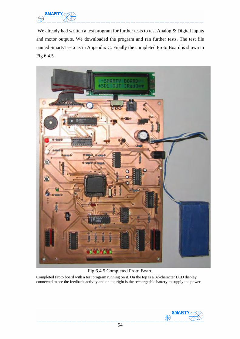
54
We already had written a test program for further tests to test Analog & Digital inputs
and motor outputs. We downloaded the program and ran further tests. The test file
named SmartyTest.c is in Appendix C. Finally the completed Proto Board is shown in
Fig 6.4.5.
Fig 6.4.5 Completed Proto Board Completed Proto board with a test program running on it. On the top is a 32-character LCD display connected to see the feedback activity and on the right is the rechargeable battery to supply the power

55
Chapter 7
The Main Board Design The main Smarty Board is a manufactured board with all the facilities of a
commercially available PCB. It was designed with cost saving measures and had a
high density of components on it. The shape and size of the board was similar to
PC104 standard used for embedded system computers. Unlike Smarty Proto it was
made with ‘plated-through’ holes having 666 holes altogether. This board has all the
components of a small robot on a single board including the RS232 interface.
7.1 Cost Reduction Measures
Cost cutting techniques were used wherever possible throughout the design. When
designing the main Smarty Board a lot of other factors were considered that were not
done during prototyping. The reason for this consideration being that the main board
was to be manufactured away from the university facilities at an industrial
environment. Here all the industrial manufacturing factors were to be included in the
design to make it cost efficient. In Appendix A a list of the manufacturing constraints
is given from our PCB manufacturer. After analysing these constraints, we found that
there were several variables to be taken into account for manufacturing the boards at a
low cost. The important factors are:
• The size of the board
• Number of plated through holes in the board
• Number of tracklayers on the board
• Type of non tracklayers
• Tooling and routing
• Colours of masks
• Number of boards per panel
We did not need our board to be of any special shape to fit into a particular chassis so
we had a freedom of keeping it to basic rectangle shape. We chose the following
options after a careful consideration of the manufacturing constraints:
• 10600mils by 16600mils panel size

56
• Double sided board
• 5-day mode
• Solder mask and Overlay
• Less than 15 tools
• Less than 8000 holes
• No stacking of panels
These options were best for pricing since we did not require any special features. The
size of the panel and the amount of holes in it were major factors for us to work on.
We did not want to waste any space that we were paying for and we used all the
facilities that were available at no extra cost. We came up with a workable size of the
board that would fit exactly twelve times in the panel taking into account the
separation-routing (cutting) space. The best size of what later became the Smarty
Board was 4000mills by 3400mills. Since there were twelve boards in a panel and the
panel had to have not more than of 8000 holes, each board should have less than or
equal to 666 holes. In Appendix A, Fig A.4.1 shows the structure of a PCB
manufacturing panel with 10600mils by 16600mils usable space for placing all
PCB’s. Fig A.4.2 displays how 12 Smarty Boards were fitted in that space with a
small amount of routing clearance for separating the boards from the panel and one
another.
The number of holes (8000) was determined in the following way: the board was
simulated first using a reliable practical algorithm on Protel and the track routings
were known. The algorithm was based on two factors, the first being the design rules
given in Table 7.3.1 and second an entity called flexibility. The flexibility was to
instruct the simulator to accept some pre-routed tracks before auto-routing. These
tracks were placed on those places were auto-router might not pass through because of
the set design rules. It meant that the layout and planning processes that are explained
later in Section 7.2 and board routing in Section 7.3 of this chapter were actually done
earlier. Protel offers this technology and more, the actual proposed board could be
previewed with full colours and components in this simulation. Having a double sided
board with hole through components and the density of the components were known
to us we ran the simulation program several times each time with minor adjustments
57
in component layout. The best we came up with was 670 holes. We saved all the
coordinates of component placing and orientation for that simulation as our final
layout. Since 666 is very close to 670 we knew that we will straighten few tracks and
corners manually to reduce it down by four. Past experiences actually help in these
types of situations. This saving in cost was important for a large amount of boards
were to be made later and for distribution throughout schools for pilot study.
7.2 Layout of Components
As it may have been clear that the processes of component laying and routing was
actually done earlier as mentioned in Section 7.1 while we were simulating the board
to get the amount of holes. But in that section only the manufacturing constraints were
mentioned. Other constraints for board making are given here. The components were
to be mounted on specific locations on the board so that all the accessibility and
interfacing to outside connections as sensors, motors, power input, battery and host
computer be easily done. Also power switch, control buttons, LCD display and other
LEDs were to be in suitable places. The placing of the components should be such
that all the required tracks must physically pass through and all connections to be
established on the board. Since we were to make a board only with two tracklayers the
layout of components and orientation of parts were the only variables we could ‘fine
tune’. A slight change in component co-ordinates actually changed the tracks passing
and hence changed the number of holes on the board. We ran many simulations with
slight changes in component layout and saved the properties for each one of them.
Finally the layout that produced the best track passing and had the lowest number of
holes was selected as our layout design. The set-up that was the final became the
component layout of Smarty Board. Since we had the components only on the top
layer of our board the ‘top overlay’ layer became the component layout, as shown in
Fig 7.2.1

58
Fig 7.2.1 Component Layout: Smarty Board The top overlay layer of main Smarty Board. The component density was high on this board so complexity of tracks was expected to be dense for there are only two tracklayers.
7.3 Board Routing
As mentioned in Section 7.2 board routing was also done during simulation of cost
cutting measures for manufacturing. There we had focused on manufacturing
limitations and constraints, here we will discuss about the board routing matters. As
this board was much different from the Proto board, design rules had changed
altogether. Here unlike the proto board there was a facility of plated through holes,
which was an advantage, but at the same time there was a huge reduction in available
space. Also there were more components on this board for all the decoupling
capacitors that were plugged in under the IC sockets had to surface as separate
components on the top layer. To make all this possible, the signal tracks had to be
made thinner and the via size smaller. Also the footprints of most of the ICs reduced
to small round in shape (please note that only pin 1 of the IC pads are kept square in

59
shape for component orientation purposes). To satisfy these needs a new footprint
library was made just for this board.
The saved Netlist from the prototyping process was ported over to make the
connectivity on this board. This is the most important task, for any change in Nets will
cause problems. The saved NetList was the final configuration of the working
prototype. Normally in the workplace situation in the industry this Netlist file gets
saved and date and time recorded; and the file properties set so that it cannot be
changed. If there are team of members accessing design files security could be used as
given in Protel Design Explorer [25] regarding tracks of members and usage.
After the net connectivity was available the design rules for the boards track/vias
were set as shown in Table 7.3.1. The properties of pads of components are already
defined in Protel during making of the Footprints so they are not included in this
table. After setting was complete the board was auto-routed several times and the best
routing output was selected. This output came up with a total of 670 for pads, vias,
and other holes such as board and component mounting. Later we manually fine-tuned
and straightened some tracks and reduced the holes to our magic number of 666.
Table 7.3.1 Width and Clearance Constraints for Design Rules The nets that carry higher current need wider copper conductor than normal signals; this has to be set before routing the board. Power circuits are the nets that carry highest current on a board.
Design Rules Variable Name Properties Set
Clearance 10mil for the entire board Routing Vias Round, Hole = 15mil (10 - 20)mil, Size 30mil Routing Topology Shortest path Net- GND 30mil (20min - 30max)mil Net- VCC 30mil (20min - 30max)mil Net- MGND 30mil (20min - 30max)mil Net- VSS 30mil (20min - 30max)mil Power Nets 40mil (30min - 40max)mil Net- Board 10mil (10min -12max)mil for the remaining nets on board

60
7.4 Final Board
After all the routing was done, work of CAD operation was over. The files were
emailed for manufacturing, we requested for a single panel run initially. Since we had
selected the 5-day mode (another cost saving exercise) with our manufacturer we had
5 clear days of working on something different; we began writing programs for
running on our future-testing phase.
As the boards came in we found that they had something extra, they were gold plated,
we did not opt for that option. The bare board is shown in Fig 7.4.1. We soldered the
IC sockets first and all the remaining components later. We did not plug the ICs in the
sockets yet. As a precaution we ran the connectivity tests of Chapter 6, Section 6.4 to
see if everything was as we had requested for manufacturing. The board passed the
test and we plugged in all the ICs and began running the test programs that we written
few days earlier. The completed board is shown in Fig 7.4.2.
Fig 7.4.1 Manufactured Bare Board The manufactured board is with double sided tracks and has plated through holes. The white colour displays the top overlay layer (a copy of board component layout) and the green colour is the top solder mask. Gold plating was a bonus from our manufacturer.

61
Fig 7.4.2 Completed Smarty Board After all the soldering the integrated circuit chips were plugged into the sockets to complete the board. It was a complete single robotic controller board with all the peripherals required including communication with the host computer. The set up here is for controlling two motors, with option to control two more by an extra chip, the chip could be inserted in the vacant socket just top/right of the micro-controller.
62
Chapter 8
Experimenting and Testing the Board Once we had assembled a complete Smarty Board we began testing it for its various
functionalities. The beginning tests were mostly with the chassis that I had developed
when experimenting with Handy Board. Two robots were built, one on wooden
chassis another on specially fabricated metal chassis. The one with wooden chassis
was a very simple robot called Smarty-Basic, made with few components including
micro-switches as sensors. The second robot was the Smarty- Standard. This was a
very different from the Smarty-Basic for it uses IR sensors that the basic robot did
not. The building, programming and testing of these robots are discussed in this
chapter.
8.1 Smarty – Basic
When I was visiting high schools to present them with the progress of this robotic
project I took some of these test modules to give them demonstrations of what they
may be involved in a near future. The participants of these demos included both the
teachers and some students who had keen interest in robotic work. During these
activities a student gave me suggestions of what he might do if he had a chance of
making of his own project using a Smarty controller board. Initially I had no keen
interest in that student’s idea, but later for the sake of learning feedbacks from
learners to me as an instructor, I had qualitatively interviewed the student. This
particular interview became one of the most important steps in developments of
Smarty Basic. He had put forward to me the making of a programmable mobile robot
with a very small number of mechanical components. He was a grade nine student
therefore I did not expect much detailed ideas from him. After I had analysed the
student’s ideas and merged with practical possibilities, I had a clear picture of what
needs to be done. His suggestion was to make a robot with two drive motors as
actuators and just two switches as sensors for sensing obstacles, mounted in front of
it. This basic unit was just to dodge any obstacles that came in front of it and keep
moving around, all that was to be taken care of by the programming part of the

63
project. The student did not explain much about the wheel drive mechanism to be
employed in his design and I did not pose all those complexities to him at that stage.
Actually I facilitated him with some parts that I had in my toolbox for him to show me
as to how he might attach the wheels to the robot. The student tried to mount the
wheels directly to the motor shaft, giving me an indication of what the student
understood about robotic locomotion. As from my experience the drive system is the
most troublesome area in robotic design. Here the wheel speed and motor speed has to
be matched to get enough torque and control in movement.
When I summed up all the innovative ideas of the student as he demonstrated to me
by his sketches and ‘show-&-tell’, I began refining it to make a design that could be
practically implemented. To use mechanical switches as sensors was a very bright
idea because it would be very simple and easily interfaced through digital inputs of
the controller board. Also there would be no need for the LCD after the programming
has been tested and finalized since there would be no need for initialization of sensor
input levels. As in Smarty Standard (Section 8.2 of this chapter) analog sensors of IR
type were used and they were to be initialized for different lighting environments. The
only area that needed to be worked out was the wheel drive mechanism. I began
looking for small motors that had a gearbox head with suitable reduction ratio. Also
the motors had to be suitable to be driven with the motor controller used on Smarty
Board. I did not want to complicate the design issues of this basic robot by mounting
gears around the wheels and posing a difficulty to learning issues. I wanted to keep it
as simple as possible the way this student had put forward to me. With the help of
MIT’s researchers I found a motor with a suitable gear head reduction ratio and drive
current. I disassembled one of those motors after purchasing few of them for study
purposes and found the gears inside in them were made from metal and not of fast
wear materials such as plastic as is the case in most of the products in the market
today. With this motor assembly the wheel could be directly attached to the output
shaft since it made about one revolution per second when used with an 8.2volts or
9.6volts supply as the battery supply used on Smarty Board. The motor assembly unit
could be easily purchased on the web at a fairly small cost. Designing the Smarty
Basic was straightforward since there are very few parts in it, they included:
• A Smarty Controller board.

64
• A battery (rechargeable 8.2V Nicad or NiMH recommended for longer
experiments and reuse).
• Two micro-switches as sensors wired with a miniature 2 pin plug spaced 100mil
(2.5mm) apart.
• Two brackets made from metal to hold the motor assembly.
• A small trailing wheel to keep balance. This could be made from any basic
material as plastic since there very little pressure exerted here.
• Two wheels made from wood and rubber tubing placed over them for better grip
(the tubing was a small piece of bicycle tube of suitable thickness).
• Nine 2.5mm in diameter, 25mm long machine screws with nuts.
• The only other thing needed was to mount all of the above parts together. I
began with making a suitable chassis for mounting all parts including the
controller board. I used a plywood measuring 85mm by 110mm and 5mm thick.
All of the above materials are shown in Figs D.1.1 to D.1.8 in Appendix D.
8.2 Assembling Smarty-Basic
Care was taken when designing the parts layout to keep it simple and minimize the
quantity of mounting screws used. Layout was made in way so that two or more units
could be fastened together on the chassis by a common screw. One end of each motor
brackets and sensors are tightened together by the same screw. The assembly was
started with drilling the holes on the chassis with counter sinking all screw heads to
keep surface clearance available for other units. On top of the wooden chassis was the
Smarty Board with a clearance of about 15mm. In the clearance space the battery
could be housed. To keep this clearance, spacers made from plastic tubing such as
housing of old ballpoint pens cut to size, any plastic tubing material could be used.
These types of spacers are easily available and could also provide insulation in case of
metal chassis was used. At the bottom side of the board the sensor switches were
mounted together with the motor assembly and the trailing wheel.

65
Wiring was very simple, the left motor was connected to motor_0 port and the right
motor to motor_1 port. The signals: the left sensor switch was connected to digital_7
port and the right to digital_8. The battery was connected to the battery port of the
controller board. We used a 8.2V NiMH rechargeable battery for economical reasons.
Since the basic unit uses only two motors, mounting only one motor controller chip on
controller board could further bring down cost. It took me about two hours in all to cut
and shape the wheels, cut the chassis to size with drilling and counter sinking, cutting
spacers, soldering the wires and assembling the entire basic unit together. That was
after all planning, designing and layouts. Shown below is the final assembly of
Smarty- Basic with all the connections made and ready to go for the programming
phase.
Fig 8.2.1 Assembled Smarty-Basic Smarty-Basic board can have only one of the two motor controllers plugged into the board as shown above. This is because one L293D controller can control two motors in both forward and reverse directions.

66
8.3 Programming Smarty-Basic Only one type of testing has been done so far with this basic unit. The test had been
on simple obstacle avoidance. The algorithm for this program was based on the
following logic levels available on sensors:
Left Sensor Right Sensor Action to be taken 0 0 Move forward 1 0 Go back ‘n’ steps and turn right 0 1 Go back ‘n’ steps and turn left 1 1 Go back ‘n’ steps and turn right (or left)
Table 8.3.1 Algorithm for Programming Smarty Basic One would imagine that ‘steps’ in Table 8.3.1 would be based on distance moved, but
that was not the case here, since stepper motors would be required for such a job. The
value for ‘n’ here is translated in time value (in seconds) since normal DC motors
were used in this project. The value could be altered in the program in case a different
motor is used or the wheel diameter gets changed to another size. Larger diameter
would reduce the value of ‘n’ and a smaller wheel diameter would need an increase.
This is because the larger wheel would cover a longer distance in a revolution in given
time. The test program written in Interactive C can be found in from Appendix C.
Tests done on Smarty Basic proved that this basic unit performed much better that
what was aimed at the beginning of this testing phase. A complete live movement of
the demonstration could be seen from the following link:
http://sky.fit.qut.edu.au/~singhr/smartyboard/Avoid_Basic.mpg.
This basic unit was capable of performing more than just obstacle avoidance. With an
IR mounted at a suitable point pointing downwards could make it into a line following
robot. Smarty Basic is aimed for middle school learners where basic construction of
mechanical parts mostly from wood and some metal shaping is involved. Assembly is
quick and effective; learners will not get bored and stay focused with the progressing
steps. Programming will be fun for them, since this would be the longest phase in
their problem solving, experimenting and learning with robotics.

67
8.4 Smarty - Standard
Some of the experimentation and development work on Smarty-Standard was carried
on the Handy Board. At that time Smarty Board was still on the drawing table. To
begin with, a suitable chassis was designed and constructed out of metal. The idea
was to make a robot chassis as flexible as possible with an open mind so that it could
be developed and modified in any direction that the experiments would show possible.
The chassis was to support the motor and drive assembly, space for mounting of the
controller board and enough space to house the battery. It was not to support any
cosmetic extensions such as outer cover/jacket or anything to improve the looks of the
unit. At that stage our efforts were directed to solve the technical and design problems
and make something simple that functions as required. Since there is no covering over
the robot all the parts and wires could be easily accessed when working with the unit.
The fabrication of the chassis was simple i.e. a piece of sheet metal folded at 90
degrees at the sided and holes drilled and threaded to mount screws as shown in
Appendix D. Two small motors with a small gear-head were chosen to provide drive
actuations. The speed reduction ratios in these motors were not enough to drive the
wheels directly, so these motors drive a final gear that was used to drive the wheels.
The wheels assembly is also shown in Appendix D (Figs D.2.3 and D.2.4).
Smarty-Standard was designed to perform more complex tasks than Smarty-Basic.
When designing the chassis parts care was taken to include some flexibility features in
case of changes were to be made to chassis. One of those was the inclusion of a
bumper bar in from of the robot as a separate attachment to the chassis. If the
experiments that were carried out would suggest changes or alterations to be made,
would only affect the bar and not the whole chassis. Throughout the experimentation
process, three different bumper-bars were made in all. The first one carried only two
sensors as shown in the robot of Fig 8.4.1. The idea was to keep the design as simple
as possible with minimum number of parts. I had an idea of trying out its
functionalities with only two sensors for sensing the obstacles in the front. The twin
sensor setup did have a good performance when the robot did a maze test but it was
not very effective for sensing all the obstacles in front of the robot.

68
Fig 8.4.1 Maze Test
The video clip of Maze test could also be viewed at this link:
http://sky.fit.qut.edu.au/~singhr/smartyboard/MazeTest.mpg
The next step was to build a bumper bar with four sensors. Two sensors were
mounted in the front and the other two on the sides. The front ones were to sense the
obstacles seen in the front and the side ones were to keep the robot a certain distance
away from the side obstacles. The assembled and wired bumper bar is shown in Fig
D.2.2 in Appendix D.
8.5 Assembling Smarty-Standard
All that is required to assemble a Smarty-Standard Robot is displayed in Appendix D.
(Fig D.2.1- D.2.A). As this was different from the Smarty-Basic and has more parts
though the wheels were made in the same way as in the Smarty-Basic. But the wheels
were assembled with a large speed reduction gear on a drive shaft of steel of about
3mm in diameter as shown. This was needed since here a different set of gear-head
motors were used. The Robot assembly begins from the chassis fabrication of mild
steel. The assembled wheels just fit in the chassis from sides as the drive shafts make
their way in the holes made in the chassis. There were no bearings used in this case to
keep it cost effective and simple. Small pins made from metal such as 1mm thick
paper clip lock in the wheel shafts. Remember that there is a third trailing wheel also

69
to be mounted for keeping balance. The chassis was turned over and the remaining
parts are fitted on top. To begin, the top components the bumper bar was placed in the
front and motors were mounted by mounting brackets as shown; note the brackets
have oblong holes so that the motors gears teeth match with the wheel gears teeth by a
small adjustment by sliding the brackets. The screws of the motor brackets also fasten
the bumper bar.
A bracket was used to mount the controller board, view the board mounting in the
photograph (Fig 8.5.2) and the bracket in Fig D.2.7 (page 107). A special ‘V’ IR
sensor was mounted on the bumper bar in the front, this sensor points downwards to
sense the information from the floor. The battery just fits behind the motors under the
board to complete the assembly. Electrical connections for this setup are given in
Table 8.5.1. The completed Smarty Standard is shown in Fig 8.5.2.
Port Connection Motor 0 Left Motor Motor 1 Right Motor
Analog 6 Floor Sensor Analog 5 Left-Front Sensor Analog 4 Left Sensor Analog 3 Right-Font sensor Analog 2 Right Sensor
Table 8.5.1 Input Output Connections: Smarty-Standard All the sensors that were mounted on the bumper bar of Smarty-Standard get connected to the analog ports of the board. Also the two motors are connected to motor port 0 and 1. Note that other analog ports are still available for any other expansion.

70
Fig 8.5.2 Assembled Smarty-Standard Smarty-Standard has 4 sensors for managing obstacles in front and sides. It has one sensor to scan the floor, which can be used to follow a dark line. Many different functions could be achieved through skilful programming techniques on this robot.

71
8.6 Programming Smarty-Standard
A number of programs were successfully run on this setup. They included inverted
pole balancing, line following and some basic levels of obstacle avoidance. The most
exciting was the line following. The code for this line following can be seen in
Appendix C of this thesis; we used a very unusual step for this robotic function. As it
may have been clear from the report so far that there was only one sensor used for
floor information in building this robot. Most of the robots that do line following use
two sensors to sense the line, one on each of the edges of the line and the line
thickness has to match the sensor separation on the robot. We managed to do
something better and more economical in our design. Better in a way that our Robot
could be able to follow any line regardless of thickness and economical that it would
use a single sensor device and not two. The trick to our case was not to sense the
entire thickness but just one of the fine edges of the line; we achieved that in our
programming. The algorithm for line following was as follows:
• The analog norm position to be initialized at the edge of the line that is
to be followed to start with.
• As far as the robot senses norm value (with a small tolerance) it keeps
moving straight ahead.
• As soon as the sensed value increases above norm, one of the wheels
runs slower than the other so that it can turn towards the line (Robot
had gone in less darker space).
• As soon as the sensed value droops below norm, one of the wheels
runs slower than the other so that it can turn away from the line (Robot
had gone in more darker space).
Our tests showed that the demonstration of this program worked better than what was
expected. The code of this program is in Appendix C. To view the line following here
is the movie clip: http://sky.fit.qut.edu.au/~singhr/smartyboard/LineTrace.mpg. The
demo became even more interesting when we decided to make Smarty to follow a
more complex line with sharp turns. We found the robot very efficiently negotiated

72
the corners and continued following the line with no errors. The movie clip for that
demo is here: http://sky.fit.qut.edu.au/~singhr/smartyboard/LineSTrace.mpg.
At this time we are trying more experiments with Smarty-Standard; there are some
experiments not completed yet. The idea was to provide this robot with some
autonomy of travel in an environment such as a walled room; it was to find its way
out of the room. A video clip of this partially completed experiment can also be
viewed here at this link: http://sky.fit.qut.edu.au/~singhr/smartyboard/ObstaclAvoidS.mpg.
73
Chapter 9
Discussion and Conclusion
A paper on Smarty Board has been submitted and accepted by The Third International
Symposium on Autonomous Minirobots for Research and Edutainment to be held in
Fukui, Japan in September 2005. Our robotic projects received a wide coverage in the
media. Articles with photos appeared in ‘The Age’ and ‘Sydney Morning Herald’ on
28th of June 2005 and in different editions of Quest Community News outlets in
Queensland in 2nd and 3rd weeks of June 2005. A live interview about discussions on
Smarty was also broadcast on ABC Radio nationwide on 28th June 2005 at 1330hrs
Eastern Australian Time.
Though the design of the Smarty Board was inspired by the schematics of the MIT’s
Handy Board, we made some significant modifications as shown in Table 9.0.1.
These changes required redrawing of the schematic as shown in Appendix B together
with schematics of Handy Board and Finger Board. There are two schematics of
Smarty Board given, the first one ‘Smarty Board A’ is the one that has been used in
most of the discussions throughout this thesis and the second ‘Smarty Board B’ is the
one we started with. The main difference between the two is that the second schematic
uses transistors and passive components for RS232 level conversion whereas the first
schematic used Maxims MAX232 chip. Initially we were not able to source the
Maxim chip but later we found them cheaply and as well as on old electronic boards.
Both of these circuits efficiently perform the tasks.
We have mostly relied on the Motorola MC68HC11A1 micro-controller throughout
our discussion in this thesis. That does not mean that other micro-controllers in that
range cannot be used. We had used the A1 series for it is the most economical in the
range and its performance is adequate in this particular case. Table 9.0.2 displays
others in that range that can be used except for MC86HC711D3. This particular unit
does not have the analog to digital conversion facility that is required in out design.

74
Table 9.0.1 Diversions from Handy Board to Smarty Board
MC68HC11 Series ADC EPROM ROM RAM EEPROM CONFIG MC68HC11A8 8x8bit * * 256 512 $0F MC68HC11A1 8x8bit * * 256 512 $0D MC68HC11A0 8x8bit * * 256 * $0C MC68HC811A8 8x8bit * * 256 8K+512 $0F MC68HC11E9 8x8bit * 12K 512 512 $0F MC68HC11E1 8x8bit * * 512 512 $0D MC68HC11E0 8x8bit * * 512 * $0C MC68HC11E2 8x8bit * * 256 2K $FF MC68HC711E9 8x8bit 12K * 512 512 $0F MC68HC711D3 * * 4K 192 * N/A MC68HC711F1 8x8bit * IK 512 $FF MC68HC11K4 8x8bit * 24K 768 640 $FF MC68HC711K4 8x8bit 24K * 768 640 $FF MC68HC11L6 8x8bit * 16K 512 512 $0F MC68HC711L6 8x8bit 16K * 512 512 $0F
Table 9.0.2 Motorola 68HC11 series Micro-Controllers When using a micro-controller from this listing please note the config register values when downloading to the board in strap-mode. Some Interactive C applications automatically configure this but IC4.30 does not.
Modified Item Handy Board Smarty Board
Boards 2 boards (Zap board and a Main board) Single Main board
Main Board Dimensions
3.25"(83mm) X
4.37" (111mm)
3.4"(86mm) X
4.0"(102mm)
Memory IC 32KB Static RAM
62256CL-100 DIP-28
32KB Static RAM W24256AK-15
P-DIP 28 SKINNY Passive Resistor
Components SIL Resistor packs Resistor packs and discrete resistors
Exclusion ZAP - Fast battery charging circuit
Inclusion Supply decoupling capacitors for every
IC Serial comms. port
Connector RJ11 to Zap Board
to DB25 3 way mini phone
socket
RS232 Circuit Placed on Zap Board
Placed on Main Board

75
In Chapter 2, we had discussed about the recycling of components from older
computer boards, we had collected large quantities of static RAMs and we had used
some of them in our design. In our discussions we mostly relied on Winbond’s
W24257AK–15 but later when we had some spare time we began collecting
datasheets and testing out others from our large pile of static RAMs. In fact most of
them worked, a list of different memory chips that could be directly fitted into the
board (identical pin connections to Winbond) is given in Table 9.0.3.
Manufacturer Chip Source
Alliance AS7C526 - 15PC 486 MainBoard cache Mosel MS62256A - 25FN 386 MainBoard cache AT&T ATT7C185P - 20 486 MainBoard cache Sony CXK5863P - 25 386 MainBoard cache Texas Instrument CY7C199 - 20PC 486 MainBoard cache Winbond W24256AK-15 486 MainBoard cache
Table 9.0.3 Static RAMs with Identical Packages and Pins These memory devices that could be used in Smarty Board directly. The column in right shows the computer boards and location they were removed from.
9.1 Recommendations for Future Modifications
We would like to make the following recommendations. We found some limitations
during the testing phase when we tried to put our robots into tougher and longer
activities. Also we want our project to evolve into new directions. Here we are stating
the recommendations and the reason we found for this future activity:
• At present the sensor supply of our board is connected directly to the 5V rail.
During testing and experimentation we found that the battery drain due to LED
supply to sensors was very high. The battery did not last for very long for sensor
LEDs are on all the time from the moment the board is switched on. We would
like to recommend that in the future designs this could be looked into to increase
the efficiency of the design. If the sensor LEDs gets switched on just few
microseconds before the IR sensors are read and switched off after the reading, the
battery drain would be very small for sensor LED load. As we understand this
modification would be both on the hardware as well as on the software. A small

76
hardware switching circuit would supply the 5V to sensor LEDs and the circuit
could be software switched.
• Another recommendation is to add a brake facility to motors. As at present neither
the hardware has braking facilities nor do the Interactive C applications support
any sort of solutions. We believe that the hardware circuits associated with the
motor controllers have to be changed and then the braking programs included in
the software.
• At present the motor controllers are to drive small motors only. This is good
enough for applications that we had targeted for. The time we had finished this
version of the work, we began experimenting for longer periods to test the
strengths of our robots. The present version of our robots barely can carry their
own weight if the battery used is large (as we had placed a larger battery for
experimenting for longer periods). In a near future a larger robot would be needed
that can carry itself as well as some instruments such as a robotic arm. For such
applications a bigger drive motors with suitable motor controllers would be
needed. Some work has been done in [1] for this area with Handy Board; a more
centralized design is recommended.
Finally anyone who has done a moderate size project in electronics would know that
there is more than ninety percent chance the project will not work when turned on for
the first time. This is one of the reasons why so many electronic engineering graduates
do not become engineers. They are disheartened by their first unsuccessful
experience, and rapidly they lose faith and avoid practical work. Their initial intention
was to become a practical engineer but they end up having to take up a semi-technical
profession. A proper set of testing procedures and parameters are required to locate
and rectify errors through small steps before powering the entire project unit. The
methodology of these test procedures varies from engineer to engineer; there is no
standard rule for this type of activity. Our methodology through this thesis would give
some insight for future learners of practical microelectronics. To learn technology one
has to enjoy making his/her hands ‘dirty’ by actually making the technological
commodity, as stated in [11] “….the most powerful way to learn technology is to
become a creator of technology”.

77
Glossary ADC Analog to Digital Converter Cct Circuit (electrical connectivity) CMOS Complementary Metal Oxide Semiconductor CPU Central Processing Unit DAC Digital to Analog Converter DIL Dual In Line package DUART Dual Universal Asynchronous Receiver and Transmitter EEPROM Electronically Erasable Programmable Read Only Memory EPROM Erasable Programmable Read Only Memory Footprint Copper circuit on a PCB for an electronic component to be placed on Hole through Type of component footprint that is connected to two or more layers IC Integrated Circuit I/O Input Output IR Infra Red LCD Liquid Crystal Display LED Light Emitting Diode MCU Micro Controller Unit MIDI Musical Instrument Digital Interface Mil Unit measurement used in Protel.(DIL pin separation =100mils) Net A node or junction for electrical connections Netlist Centralised collective information of all the nets of a schematic Pad A plated through hole on a PCB for external connection PC Personal Computer PCB Printed Circuit Board PGA Pin Grid Array PLCC Plastic Leaded Chip Carrier RAM Random Access Memory ROM Read Only Memory Rx Receiver SCI Serial Communication Interface SPI Serial Peripherals Interface SRAM Static Random Access Memory Surface Mount Type of component footprint that is just on one side of the board Tx Transmitter TTL Transistor-to-Transistor Logic Vias Holes on PCB (with holes or blind) that are plated through with copper, providing connections in between track layers Table 9.2.1 Table of Abbreviated and Technical Terms

78
Appendix A A.1 Specifications 79 A.2 Bill of Materials 81 A.3 Manufacturing Constraints 82

79
A.1 Specifications General Board Name: Smarty Board Version: Version 1.0 Release Date: 01-08-2004 CAD used for design: Protel Design Systems PCB Filename: SmartyBoard1.pcb Schematic ref: SmartyBoard1.sch Designed by: Raj Singh Mechanical Board shape: Rectangular Dimensions: Keep-out-layer 3400mils X 4000mils (86.4mm X 101.6mm)
Mounting holes-120mils dia.(approx 3mm) inside Keep- Out-Layer 3100mils X 3700mils (78.5mm X 93.6mm)
Track Layers: Double sided Components Density: 17 Integrated Circuits on board Component mount type: Plated through holes Electrical Micro Controller: Motorola 68HC811A1 clocking at 8MHz. I/O: Inputs- 7 analog, 9 digital Outputs- 4 actuators (motors and solenoids) Output Level Control: Pulse-width-modulated- forward and reverse -10 steps Input Control: 2 switches- push button (STOP and START) Power switch - slide Display and Feedback: LCD 16 characters X 2 lines, Battery low indicator LED Power on indicator LED, Signal Rx LED Motor Forward/Reverse LEDs, Battery charge LED Multi tone buzzer External Memory: SRAM 256Kbits (organized as 8bit words X 32K) Power Requirements Powered by 9.6Volts rechargeable battery (NiCad or NiMH), 12Volts DC, 350mA unregulated power plug-pack Other Facilities Battery Charging: Onboard battery charging circuit PC Interface: Onboard RS232 circuit Connects to PC through Communications port using DB9 to 3mm mini-phone plug, 3 way cable for download and upload of data from the board Data Backup: Memory backs-up as long as battery stays alive. Table A.1.1 Board Specifications

80
A.2 Bill of Materials Designator FootPrint Count++ PartType Source Cost
Recycled Other with
Recycle Actual IC1 PGA52-9 1 68HC11A1 * Purchased $US1.00 5.95 IC2 FDIP28 2 W24257A X * * 21.00 IC3 FDIP20 3 74HC373 X * * 2.50 IC4 FDIP20 4 74HC374 X * * 2.50 IC5 FDIP20 5 74HC244 X * * 2.05 IC6 FDIP16 6 74LS138 X * * 1.75 IC7 FDIP16 7 L293D * Purchased $US2.50 3.99 IC8 FDIP16 8 L293D * Purchased $US2.50 3.99 IC9 FDIP14 9 74HC04 X * * 0.95 IC10 FDIP14 10 74HC132 X * * 0.95 IC11 FDIP16 11 MAX232 X * * 4.45 IC12 FTO92 12 78L05 X * * 0.75 IC13 REG 13 7805 X * * 0.80 IC14 FTO92 14 DS1233 * Purchased $US0.75 2.25 IC15 FTO92 15 ZTX614 * Purchased $US0.75 0.75 IC16 DIP-2X 16 IR-Tx X * * 1.95 IC17 SIP-3 17 IR-Rx X * * 2.55 C1 CAP-L 18 470uF X * * 0.80 C2 DIP-2X 19 104M X * * 0.10 C3 SIP-2 20 22pF X * * 0.10 C4 SIP-2 21 22pF X * * 0.10 C5 CAP-S 22 10uF X * * 0.20 C6 CAP-S 23 10uF X * * 0.20 C7 CAP-S 24 10uF X * * 0.20 C8 CAP-S 25 10uF X * * 0.20 C9 DIP-2X 26 0.0068uF X * * 0.25 C10 SIP2 27 104M X * * 0.10 C11 SIP2 28 104M X * * 0.10 C12 DIP-2X 29 22uF Tant X * * 0.35 C13 DIP-2X 30 22uF Tant X * * 0.35 C14 SIP2 31 104M X * * 0.10 C15 SIP2 32 104M X * * 0.10 C16 SIP2 33 104M X * * 0.10 C17 SIP2 34 104M X * * 0.10 C18 SIP2 35 104M X * * 0.10 Cm1 SIP2 36 104M X * * 0.10 Cm2 SIP2 37 104M X * * 0.10 Cm3 SIP2 38 104M X * * 0.10 Cm4 SIP2 39 104M X * * 0.10 R1 RES4 40 47R X * * 0.22 R2 RES4 41 100R X * * 0.22 R3 RES4 42 2.2M X * * 0.22 R4 RES4 43 1K X * * 0.22 R5 RES4 44 1K X * * 0.22 R6 RES4 45 1K X * * 0.22 R7 RES4 46 1K X * * 0.22 R8 RES4 47 2.2K X * * 0.22 R9 RES4 48 47K X * * 0.22 R10 RES4 49 47K X * * 0.22 R11 RES4 50 1K X * * 0.22 R12 RES4 51 1K X * * 0.22 R14 RES4 52 1K X * * 0.22 R13 RES4 53 1K X * * 0.22 R15 RES4 54 1K X * * 0.22 R16 RES4 55 1K X * * 0.22 R17 RES4 56 47K X * * 0.22 R18 RES4 57 1K X * * 0.22 R19 RES4 58 47K X * * 0.22 R20 RES4 59 10K X * * 0.22 R21 RES4 60 10K X * * 0.22 R22 RES4 61 3.83k X * * 0.22

81
R23 RES4 62 47K X * * 0.22 RP1 SIP-8 63 47K-7 X * * 0.90 RP2 SIP-10 64 47K-9 X * * 0.90 D1 DIP-2X 65 IN914 X * * 0.55 D2 DIP-2X 66 IN914 X * * 0.55 D3 DIP-2X 67 IN914 X * * 0.55 D4 DIP-2X 68 IN4004 X * * 0.80 L1 FSIP2 69 CHARGE X * * 0.14 L2 FSIP2 70 PWR-TX X * * 0.14 L3 FSIP2 71 RX X * * 0.14 L4 FSIP2 72 RESET X * * 0.14 L5 FSIP2 73 M1F X * * 0.14 L6 FSIP2 74 M1R X * * 0.14 L7 FSIP2 75 M2F X * * 0.14 L8 FSIP2 76 M2R X * * 0.14 L9 FSIP2 77 M3F X * * 0.14 L10 FSIP2 78 M3R X * * 0.14 L11 FSIP2 79 M4F X * * 0.14 L12 FSIP2 80 M4R X * * 0.14 L13 FSIP2 81 IR-Tx X * * 0.14 F1 DIP-2X 82 1A Fuse X * * 0.90 RV1 POT 83 22k X * * 0.24 J1 PWR-IN 84 Power In X * * 1.20 J2 PHONE-J 85 Coms In X * * 2.50 J3 BSIP-16 86 LCD X * * 0.70 J4 SIP-2 87 Battery X * * 0.70 J5 BSIP-7 88 ANALOG X * * 0.70 J6 BSIP-9 89 DIGITAL X * * 0.70 J7 BMOTOR-4 90 MOTOR X * * 0.70 J8 SIP-10 91 X * * 0.70 J9 SIP-6 92 SS X * * 0.70 J10 BSIP-9 93 DIGITAL + X * * 0.70 J11 BSIP-9 94 DIGITAL - X * * 0.70 J12 BSIP-7 95 ANALOG+ X * * 0.70 J13 BSIP-7 96 ANALOG- X * * 0.70 BZ1 CAP-L 97 BUZZER X * * 2.99 SW1 SWITCH 98 PWR ON X * * 1.95 SW2 SW-PB 99 START X * * 0.45 SW3 SW-PB 100 STOP X * * 0.45 X1 DIP-2X 101 8.00 MHz X * * 2.75 LCD1 *** 102 MTC-C162 * Purchased $US9.50 15.95 JxIC1 PGA52-9 103 Socket * Purchased $US1.00 1.95 JxIC2 FDIP28 104 Socket X * * 0.99 JxIC3 FDIP20 105 Socket X * * 0.99 JxIC4 FDIP20 106 Socket X * * 0.99 JxIC5 FDIP20 107 Socket X * * 0.99 JxIC6 FDIP16 108 Socket X * * 0.80 JxIC7 FDIP16 109 Socket X * * 0.80 JxIC8 FDIP16 110 Socket X * * 0.80 JxIC9 FDIP14 111 Socket X * * 0.62 JxIC10 FDIP14 112 Socket X * * 0.62 JxIC11 FDIP16 113 Socket X * * 0.80 Battery *** 114 9.6V battery X * * 19.95 Power Pack *** 115 12V 350mA X * * 26.45 Smarty PCB *** *** PCB * * * 9.17 Board Assembly * * * * * * 20.00 Totals * 115 * 108 7 $US17.50 A197.21 Table A.2.1 Bill of Materials of the PCB Notes:
• The cost of the parts (actual costs - last column) is based on purchasing the components in packs of ten from local and international stores through the web.
• The cost of the Smarty PCB is based on manufacturing 100 panels (1200 circuit boards) with standard plating and colors.
• The cost of assembly is based on a single board (arranged by the PCB manufacturer).

82
A.3 Manufacturing Constraints BEC Manufacturing Pty Ltd
7 Walter Crescent, Lawnton, 4501 or PO Box 5282, Brendale Q 4500 Australia Ph 61 (07) 3881 1321 Fax 61 (07) 3205 5879 ACN: 070 998 284
Email [email protected] Web Site: www.becman.com ABN: 72 070 998 284
Price Effective on orders placed after 1 September, 2003
Prices DO NOT INCLUDE GST
Any job received after 12 pm (Brisbane time) will be considered to have been received the next day.
10.6" x 16.6" panels (usable area) TURNAROUND 6 DAY 6 DAY
6 Layer Solder Mask SM and Overlay Full Engineering setup (new jobs) $ 372.00 $ 412.00 OR Production setup (repeat jobs) $ 77.00 $ 104.00 PLUS Panel Cost $ 146.00 + BBT $ 148.00 + BBT BBT: depends on design and number of different circuits in the panel. As a guide, multiple identical PCBs on a panel usually calculates at $140-$170. Specific quote required. 4 Layer Solder Mask SM and Overlay Full Engineering setup (new jobs) $ 310.00 $ 350.00 OR Production setup (repeat jobs) $ 77.00 $ 104.00 PLUS Panel Cost $ 108.00 + BBT $ 110.00 + BBT BBT: depends on design and number of different circuits in the panel. As a guide, multiple identical PCBs on a panel usually calculates at $140-$170. Specific quote required. TURNAROUND 4 DAY 5 DAY 5 DAY Double-sided Bare, tinned* Solder Mask SM and Overlay Engineering setup (new jobs) $ 202.00 $ 249.00 $ 290.00 OR Production setup (repeat jobs) $ 44.00 $ 55.00 $ 82.00 PLUS Panel cost $ 63.00 ea $ 70.00 ea $ 72.00 ea Single-sided Bare, tinned* Solder Mask SM and Overlay Engineering setup (new jobs) $ 128.00 $ 162.00 $ 200.00 OR Production setup (repeat jobs) $ 22.00 $ 47.00 $ 74.00 PLUS Panel cost $ 55.00 ea $ 58.00 ea $ 60.00ea
14.6" x 16.6" panels (usable area) TURNAROUND 5 DAY 5 DAY 5 DAY Double-sided Bare, tinned* Solder Mask SM and Overlay Engineering setup (new jobs) $ 209.00 $ 259.00 $ 312.00 OR Production setup (repeat jobs) $ 44.00 $ 55.00 $ 82.00 PLUS Panel cost $ 83.00 ea $ 91.00 ea $ 93.00 ea Single-sided Bare, tinned* Solder Mask SM and Overlay Engineering setup (new jobs) $ 129.00 $ 165.00 $ 216.00 OR Production setup (repeat jobs) $ 22.00 $ 47.00 $ 74.00 PLUS Panel cost $ 69.00 ea $ 74.00 ea $ 76.00 ea *Note: Bare, tinned not suitable for track width/spacing less than 0.015inch.Freight: $12.00 per 3kg overnight satchel (Approx. 7 small panels or 5 large panels cut to satchel size) $16.50 per 5kg overnight satchel The above prices include routing, and assume the following: material 0.8, 1.2 or 1.6mm FR-4, green or white soldermask, white overlay, 1 oz (35μm) copper, 15 or fewer different sized tools (drills), AND

83
Cont…… 10.6 x 16.6 panel 14.6 x 16.6 panel max 30 boards on panel max 40 boards on panel max 4000 holes in panel max 5500 holes in panel For other combinations, please contact us for a quotation. The following charges apply to variations to the above conditions: DRILLING –Number of holes (To be charged for every stack of 1-4 panels)
10.6 x 16.6 PANELS 14.6 x 16.6 PANELS 4000 – 5500 $10.00 5500 – 7000 $10.00 5500 – 7000 $20.00 7000- 8500 $20.00
$10 for every 1000 holes thereafter (Please note that to have 4 panels per stack, hole sizes must be larger than 0.75mm)
TOOLING Over 15 tools (drill sizes) - $17.00 (one time charge per order) ROUTING or VEE-GROOVING 10.6 x 16.6 Panels – 31-60boards/panel, add $10.00 per panel. More than 60 POA 14.6 x 16.6 Panels – 41-70 boards/panel, add $10.00 per panel. More than 70 POA HAND FINISHING If boards are to be “routed out” and hand ground, then the following charges apply.
10.6 x 16.6 PANELS – add $5.00 per panel over 30 14.6 x 16.6 PANELS - add $7.00 per panel over 40
COPPER PLATING (FINAL THICKNESS SHOWN) 2 oz 4 oz
10.6 x 16.6 PANELS – $38 for 1-8 panels $60 for 1-8 panels 14.6 x 16.6 PANELS - $38 for 1-4 panels $60 for 1-4 panels. Other conditions, POA
MATERIAL THICKNESS 0.2mm 0.4mm 2.4mm 3.2mm
10.6 x 16.6 PANELS 0.00 0.00 $10.00 per panel $15.00 per panel 14.6 x 16.6 PANELS N/A N/A $15.00 per panel $20.00 per panel SOLDER MASK For colours other than Green or white, a flat rate charge of $40.00 per colour applies.
EXTRA SCREENPRINTING
Second Overlay – $40.00 setup plus $2.00 per panel Carbon Printing - $70.00 setup plus $2.50 per panel
GOLD PLATING 1-4 Panels - $145.00 5-15 Panels - $180.00 DRILLED & ROUTED BLANK PCBS
Blank laminate drilled & routed to the pattern of your pcb. FOR SMALL PANELS LARGE PANELS $50.00 $65.00

84
Fig A.4.1 Bare Small Panel Bare panel with manufacturing mounting space and 10600mil X 16600mil PCB usable space.

85
Fig A.4.2 Completed Small Panel
Small Panel with usable space filled up with PCBs. A total of 12 boards fit in the panel with no space wasted. Each board measures 3400mils X 4000mils, a small space of about 100mils is allowed in between as routing space for separating the boards.

86
Appendix B Schematics
B.1 Smarty Board A 87
B.2 Smarty Board B 88
B.3 Handy Board 89
B.4 Finger Board 90
Art Works
B.5 Top layer/Bottom layer 91/92

87
Fig B.1.1 Schematic – Smarty Board A

88
Fig B.2.1 Schematic – Smarty Board B

89
Fig B.3.1 Schematic – Handy Board

90
Fig B.4.1 Schematic – Finger Board

91
Fig B.5.1 PCB Artwork: Top layer

92
Fig B.5.2 PCB Artwork: Bottom layer

93
Appendix C
Smarty Programs
C.1 Smarty Test Program 94
C.1 Smarty Music 95
C.2 Smarty Basic (Avoidance) 96
C.4 Smarty Line Following 98

94
/********************************************************************** SmartyTest Program
Author: Raj Singh, SDL, QUT, Brisbane. There are three functions in this program, when this program is loaded on the Smarty Board in IC-4.3 environment, each of these functions can be called as interactions from the host computer. These functions are to test the I/O of the board *************************************************************************/ void smarty_digital() /*This function is to test the digital inputs, note: the inputs are numbered from 7-16, 9 of them altogether. By default the inputs are pulled to +5V by ‘pull-up-resistors’ so the display would show “111111111”. By connecting a jumper to any of the inputs and ground, they can be brought to logic 0 and hence the display would change accordingly*/ { int i; while (!stop_button()) { /* Press the STOP button on the board anytime to stop the test */ for (i=7;i<16; ++i){ printf("%d",digital(i)); } printf("\n"); sleep(0.2); } printf(" \n"); } /**********************************************************************/ void smarty_analog() /*This function is to test the analog inputs note: the inputs are numbered from 0 to 6, 7of them altogether. A variable resistor can be wired and plugged in the analog inputs and values in range of 0-255 displayed. By default the pull-up-resistors would make the inputs to 255 */ { int i; while (!stop_button()) { /* Press the STOP button on the board anytime to stop the test */ for (i=2;i<7; ++i){ printf("%d ",analog(i)); } printf("\n"); sleep(0.2); } printf(" \n"); } /**********************************************************************/ void smarty_motor() /* This function is to test the motor outputs note: the outputs are numbered from 0 to 3, 4 of them altogether; the motors are tested in forward and then in reverse. The motor LEDs would display the activity as well as the activities on the connected motors. */ { int i; while (!stop_button()) { /* Press the STOP button on the board anytime to stop the test */ for (i=0;i<4; ++i){ printf("Motor%d Forward\n",i); motor(i,100); sleep(0.5); } for (i=0;i<4; ++i){ printf("Motor%d Reverse\n",i); motor(i,-100); sleep(0.5); } printf(" \n"); alloff(); } } /**********************************************************************/

95
/********************************************************************** Smarty Music
Author: Raj Singh, SDL, QUT, Brisbane. Smarty Board can produce different tones as audio feedback too and can be used in programming for different purposes such as warnings, completion of a task etc. To test this facility a simple music was composed.
**********************************************************************/ void music() { printf(" -SMARTY BOARD- *SDL QUT (Raj)*\n"); while (!stop_button()) { /* the test can be stopped anytime by pressing the STOP button on the board */ int count=0; while ((!stop_button())&&(count != 4)) { tone(200.0,0.12); sleep(0.1); tone(200.0,0.12); sleep(0.1); tone(700.0,0.12); sleep(0.1); tone(200.0,0.12); sleep(0.1); tone(200.0,0.12); sleep(0.1); tone(200.0,0.12); sleep(0.1); tone(600.0,0.12); sleep(0.1); tone(700.0,0.12); sleep(0.1); ++count; } tone(800.0,0.12); sleep(0.1); tone(800.0,0.12); sleep(0.1); tone(600.0,0.12); sleep(0.1); tone(600.0,0.12); sleep(0.1); tone(400.0,0.12); sleep(0.1); tone(400.0,0.12); sleep(0.1); tone(300.0,0.12); sleep(0.1); tone(180.0,0.12); sleep(0.1); if (stop_button()) printf("Stop PRESSED\n"); } } /**********************************************************************/ void main() { while (!stop_button()) { music(); } printf("All Over, Switch OFF S1\n"); } /**********************************************************************/

96
/* ******************************************************************* Smarty Basic – Obstacle avoidance
Author: Raj Singh, SDL, QUT, Brisbane. This program is for Smarty Basic with two switches as sensors. Wiring: Motor 0 = Left motor with white as positive and grey as negative. Motor 1 = Right motor with white as positive and blue as negative. sensor 7 = left sensor (no polarities). sensor 8 = Right sensor (no polarities). Modification to the board: 2 X 10⁴ caps placed on L293D across pins 16-13 and 8- 4 works well....... Raj 12-09-2004 ..13:00hrs NOTE: The user can stop the Robot anytime by pressing STOP button on the controller **********************************************************************/ void back_t_right() /* If the left sensor reports problems than take a few steps backwards and then turn right */ { while (((digital(7))&&(!digital(8)))&&(!stop_button())) { printf("Turning Right\n"); motor(0,-50); motor(1,-50); sleep(1.0); motor(0,50); motor(1,0); sleep(1.5); } } /**********************************************************************/ void back_t_left() /* If the right sensor reports problems than take a few steps backwards and then turn left */ { while (((digital(8))&&(!digital(7)))&&(!stop_button())) { printf("Turning Left\n"); motor(0,-50); motor(1,-50); sleep(1.0); motor(0,0); motor(1,50); sleep(1.5); } } /**********************************************************************/ void back_off() /* If there is no way to go (all the sensors report problems) then go back where you came from */ { while (((digital(7))&& (digital(8)))&&(!stop_button())){ printf("Backing off\n"); motor(0,-50); motor(1,-50); sleep(1.0); motor(0,50); motor(1,0); sleep(1.5); } }

97
/**********************************************************************/ void go_straight() /* Keep going straight ahead till either the user strops the Robot or there is an obstacle on the way */ { while (((!digital(7))&&(!digital(8)))&&(!stop_button())) { motor(0,50); motor(1,50); printf("Forward\n"); sleep(0.1); } } /**********************************************************************/ void main() { while (!start_button()) { printf("Press Start to BEGIN...\n"); sleep(0.3); } while (!stop_button()) { go_straight(); back_t_right(); back_t_left(); back_off(); } motor(0,0); motor(1,0); printf("All Over, Switch OFF S1\n"); } /**********************************************************************/
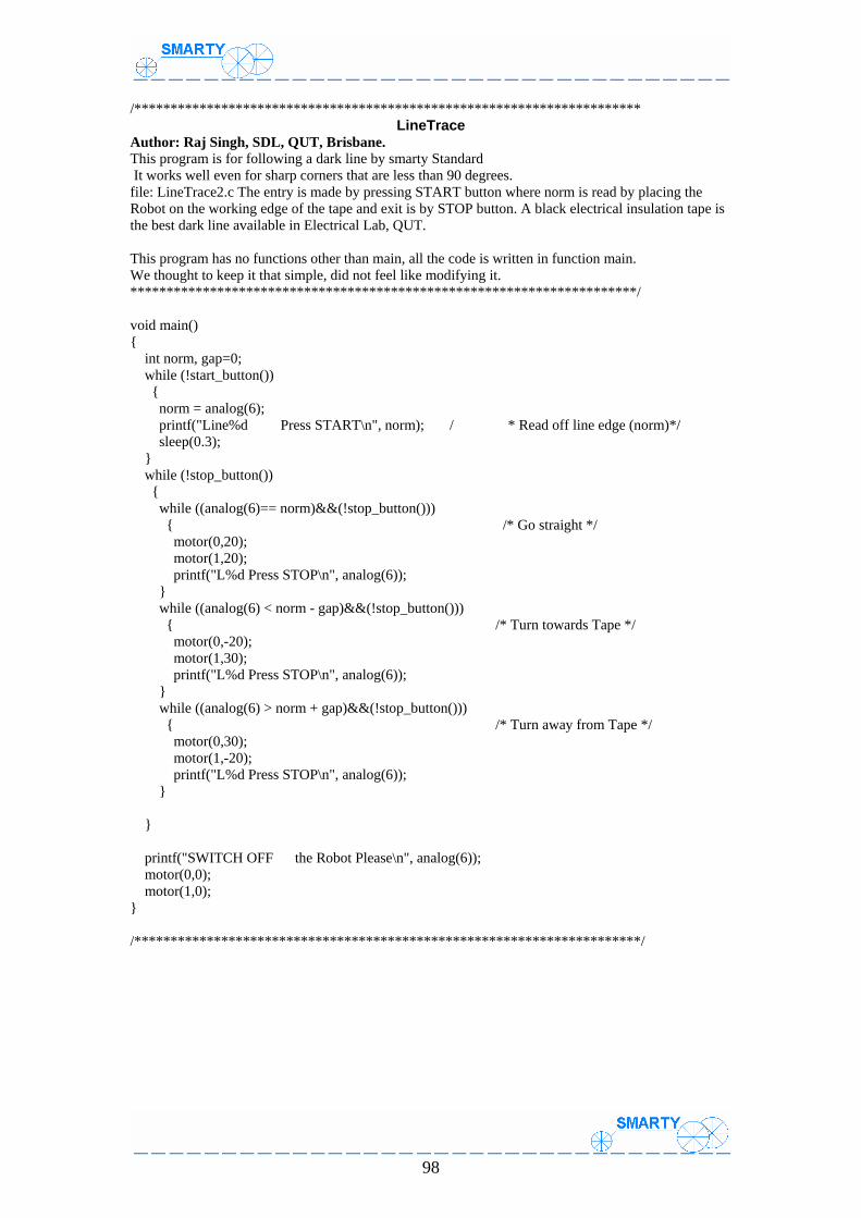
98
/********************************************************************** LineTrace
Author: Raj Singh, SDL, QUT, Brisbane. This program is for following a dark line by smarty Standard It works well even for sharp corners that are less than 90 degrees. file: LineTrace2.c The entry is made by pressing START button where norm is read by placing the Robot on the working edge of the tape and exit is by STOP button. A black electrical insulation tape is the best dark line available in Electrical Lab, QUT. This program has no functions other than main, all the code is written in function main. We thought to keep it that simple, did not feel like modifying it. **********************************************************************/ void main() { int norm, gap=0; while (!start_button()) { norm = analog(6); printf("Line%d Press START\n", norm); / * Read off line edge (norm)*/ sleep(0.3); } while (!stop_button()) { while ((analog(6)== norm)&&(!stop_button())) { /* Go straight */ motor(0,20); motor(1,20); printf("L%d Press STOP\n", analog(6)); } while ((analog(6) < norm - gap)&&(!stop_button())) { /* Turn towards Tape */ motor(0,-20); motor(1,30); printf("L%d Press STOP\n", analog(6)); } while ((analog(6) > norm + gap)&&(!stop_button())) { /* Turn away from Tape */ motor(0,30); motor(1,-20); printf("L%d Press STOP\n", analog(6)); } } printf("SWITCH OFF the Robot Please\n", analog(6)); motor(0,0); motor(1,0); } /**********************************************************************/

99
Appendix D Smarty Projects: Assembly Materials and Tools
D.1 Smarty-Basic 100
D.2 Smarty-Standard 104
D.3 Smarty Tools 109

100
D.1 Components Needed for Smarty Basic
Fig D.1.1 Two Gear-headed Motors
Fig D.1.2 A Rechargeable Battery

101
Fig D.1.3 Eight 2.5mm X 30mm Machine Screws
Fig D.1.4 Suitable Brackets to Mount the Motors and Trailing Wheel

102
Fig D.1.5 Chassis made from Plywood with Holes Drilled
Fig D.1.6 Smarty Controller Board

103
Fig D.1.7 Micro-switches as Sensors
Fig D.1.8 Wheels Cut from Wood with a hole-saw and edges rounded. A small piece of rubber cut from bicycle tube shoved on the prepared for grip.

104
D.2 Components Needed for Smarty-Standard
Fig D.2.1 Metal Prepared Chassis
Fig D.2.2 Bumper Bar with four Sensors

105
Fig D.2.3 Wheel Components: Dismantled
Fig D.2.4 Wheel Components: Assembled

106
Fig D.2.5 Motors: Gear Headed
Fig D.2.6 Motor Mounting Brackets

107
Fig D.2.7 Bracket for Mounting Controller Board
Fig D.2.8 9.6V NiMH Rechargeable Battery Pack

108
Fig D.2.9 V IR Sensor for Line Following
Fig D.2.A Smarty Controller Board with LCD

109
D.3 Tools Kit used for Robotic Work
Fig D.3.1 Tool Kit

110
Bibliography
[1] J. Munro, "Controlling the Magnevation Motor Driver Board with Handy Board,",, 05-2002 ed: Seattle Robotics Society Available: http://www.seattlerobotics.org/encoder/200205/magnevation.htm13-01-2005].
[2] R. Burns, The Adult Learner at Work. Sydney: Business & Professional Publishing,
1995. [3] "Study Area Specification (SAS) Resources: Years 11 & 12,", vol. 2002: Queensland
Studies Authority Available: http://www.qsa.qld.edu.au/yrs11_12/sas/index.html [2002, 20/01/2005].
[4] "Engineering Technology Subject Guide (2004 syllabus): Years 11 & 12,", vol. 2004:
Queensland Studies Authority Available: http://ww.qsa.qld.edu.au/yrs11_12/subjects/engineering.html [2004, 20/01/2005].
[5] "Technology: Years 1 to 10 Syllabus," Queensland Studies Authority 2002. [6] M. Barak, "Learning Good Electronics or Coping With Challenging Tasks: The
Priorities of Excellent Students," Journal of Technology Education, vol. 14, pp. 20-34, 2002.
[7] F. G. Martin, D. Butler, and W. M. Gleason, "Design, Story-Telling, and Robotics
in Irish Primary Education," presented at IEEE Systems, Man and Cybernetics Conference, Nashville, TN, 2000.
[8] F. G. Martin, "Kids Learning Engineering Science Using LEGO and the
Programmable Brick," presented at Annual Meeting of the American Educational Research Association, New York, NY, 1996.
[9] B. L. Delahaye, Human Resource Development: Principles and Practices, 1st ed.
Brisbane: John Wiley & Sons, 2000. [10] L. Porter, Student Behaviour: Theory and Practice for Teachers, 2nd ed. St
Leonards, NSW: Allen & Unwin, 2000. [11] P. Wyeth, M. Venz, and G. Wyeth, "Scaffolding Children's Robot Building and
Programming Activities," Robocup 2003, vol. 3020, pp. 308-319, 2004. [12] "Intelligent, Autonomous Mobile Robot Kits for Education, Entertainment &
Commercial,", vol. 2005: Mekatronix Available: http://www.mekatronix.com [2005, 21/02/2005].
[13] F. G. Martin, "Assembling the Handy Board," Massachusetts Institute of
Technology, Cambridge, MA, Project Assembly Manual 02-01-1997 1997. [14] "Embedded Products and Design Services,", vol. 2005: Allen Systems Available:
http://www.allen-systems.com/cp11.htm [2005, 13-01-2005]. [15] "Motorola M68HC11 Reference Manual 1991,".: Banta Co., 1995.
111
[16] K. L. Doty, "MSCC11 Single Chip MC68HC11 Microcontroller Board: Assembly Manual," Mekatronix, Gainesville, FL, Assembly Manual 08-09-1999 1999.
[17] "Embedded Acquisition Systems latest Finger Board 2.,", vol. 2005 Available:
http://www.embeddedtronics.com/computers.html [2005, 20-01-2005]. [18] F. G. Martin, "The Handy Board Technical Reference," Massachusetts Institute of
Technology, Cambridge, MA 2000. [19] K. Lynch, "ME 333 Introduction to Mechatronics Lab: The Handy Board,", vol.
2005: Northwestern University, Available: http://lims.mech.northwestern.edu/~lynch/courses/ME333/labs/lab3.pdf [2005, 13-01-2005].
[20] C. Leider, "Interactive Art with the MIT Handy Board," Dartmouth College
(Department of Music) 2003. [21] F. G. Martin and G. J. Pantazopoulos, "Designing The next Generation Handy
Board," presented at Symposium of American Association for Artificial Intelligence, Stanford, CA, 2004.
[22] C. Leider, "Realtime Midi Library for the MIT Handy Board: Functional
Reference,", vol. 2005: Department of Music, Dartmouth College Available: http:/music.dartmouth.edu/~colby/hb.htm [2005, 13-01-2005].
[23] R. Sargent, "IC 4 Programmers Manual," Kiss Institute for Practical Robotics 2003. [24] C. Savander-Ranne and S. Kolari, "Promoting the Conceptual Understanding of
Engineering Students through Visualisation," Global Journal of Engineering Education, vol. 7, pp. 189-200, 2003.
[25] "Protel 99SE Training Manual: Design Explorer and Document Editor Basics.,"
Protel International Limited 2001. [26] "Protel 99SE Training Manual: Schematic Capture," Protel International Limited
2001. [27] D. J. Paluska, "Design of Humanoid Biped for Walking Research," in Department of
Mechanical Engineering. Cambridge, MA: Massachusetts Institute of Technology, 2000, pp. 54.
[28] "Protel 99SE Training Manual: PCB Design," Protel International Limited 2001. [29] F. V. Polpeta, "LEGO RCX Hitachi H8/3292,", vol. 2004 Available:
http://www.lisha.ufsc.br/~guto/teaching/ish/processors/h8/overview.pdf [12-01-2004].
[30] "PIC FAQ "Frequently asked questions for Mcrochip PIC 8 bit Microcontroller
Programming,", vol. 2004 Available: http://www.electronic-engineering.ch/microchip/faq/faq.html [23-06-2004].