design and clocking of vlsi multipliers - · pdf filedesign and clocking of vlsi multipliers...
TRANSCRIPT

DESIGN AND CLOCKING OF VLSI MULTIPLIERS
Mark Ronald Santoro
Technical Report No. CSL-TR-89-397
October 1989
Computer Systems LaboratoryDepartments of Electrical Engineering and Computer Science
Stanford UniversityStanford, CA 94305
This thesis presents a versatile new multiplier architecture, which canprovide better performance than conventional linear array multipliers at afraction of the silicon area. The high performance is obtained by using a newbinary tree structure, the 4-2 tree. The 4-2 tree is symmetric and far moreregular than other multiplier trees while offering comparable performance,making it better suited for VLSI implementations. To reduce area, a partial,pipelined 4-2 tree is used with a 4-2 carry-save accumulator placed at itsoutputs to iteratively sum the partial products as they are generated.Maximum performance is obtained by accurately matching the iterative clockto the pipeline rate of the 4-2 tree, using a stopp:able on-chip clock generator.
To prove the new architecture a test chip, called SPIM, was fabricated in a1.6 pm CMOS process. SPIM contains 41,000 transistors with an array sizeof 2.9 X 5.3 mm. Running at an internal clock frequency of 85 MHz, SPIMperforms the 64 bit mantissa portion of a double extended precision floating-point multiply in under 120 ns. To make the new architecture commerciallyinteresting, several high-performance rounding algorithms compatible withIEEE standard 754 for binary floating-point arithmetic have also beendeveloped.
pev Words and muhipliers, multiplication, VLSI multipliers, 4-2multipliers, 4-2 trees, iterative, VLSI, Clocking.

0 Copyright 1989 by Mark Ronald SantoroAll Rights Reserved

To
My Parents
Ron and Bunny
My Brothers
Tom, Steve, and Jimmy
and
To all the friends and loved ones who stood by me throughout the many longyears of my continuing education.
. . .111


Acknowledgements
The journey through the Ph.D. program at Stanford is a long and difficult
one, often creating doubt in the minds of those who attempt it. Support and
help from friends, family, and faculty can be invaluable to the success and
mental well being of the student along the way. To begin with, I cannot
stress enough that the single most important person contributing to the
success of the student is the principle dissertation advisor. It is important to
pick an advisor who is both interested and knowledgeable in the chosen
research area. With this in mind, I would like to thank Mark Horowitz for
his help and guidance. Mark’s extensive knowledge of circuits and keen
insight into VLSI design were major assets. He asked hard questions, but
searching for the answers produced some of the more interesting results in
this thesis.
I am also grateful to the many people who influenced me throughout my
career at Stanford (sorry if I missed any of you). I guess the first person I
should thank, or blame, is Norman Jouppi, who talked me into taking my
first VLSI design class. John Newkirk and Robert Mathews did such an
excellent job of teaching the class that it really did change my life. I’ll never
forget the many all-nigh&s spent with my design partner Jay Duluk. Over
the years the numerous hours spent doing VLSI design with Jay and Jim
Gasbarro have destroyed my eyesight, body and mental faculties. But, all
kidding aside, it has truly been an, um, enlightening experience, and I am
V

thankful for having the opportunity to work with both of them. More
recently, I would like to thank Jim Burr for his input regarding 4-2 multiplier
trees. Thanks also to William McAllister and Dan Zuras for discussions on
multiplication and clocking. My special thanks and acknowledgements go to
Gary Bewick, who helped extensively with the IEEE rounding chapter. Gary
was even foolish enough to read an early copy of this thesis, making
numerous comments which greatly improved the final presentation. I would
also like to thank Mark Horowitz, Allen Peterson, Bruce Wooley, and Teresa
Meng, for serving on my orals committee, and additional thanks to Mark,
Bruce, and Teresa for reading copies of this thesis.
Last, but certainly not least, I would like to thank my family and the dear
friends and loved ones who stuck by me throughout the years. I will not
name you all, but I am eternally grateful. Words cannot express the warmth
and gratitude I feel for each of you.
This work was supported by the Defense Advanced Project Research Agency
(DARPA) under contract NO00 14-87-K-0828. Fabrication support through
MOSIS is also gratefully acknowledged.
vi
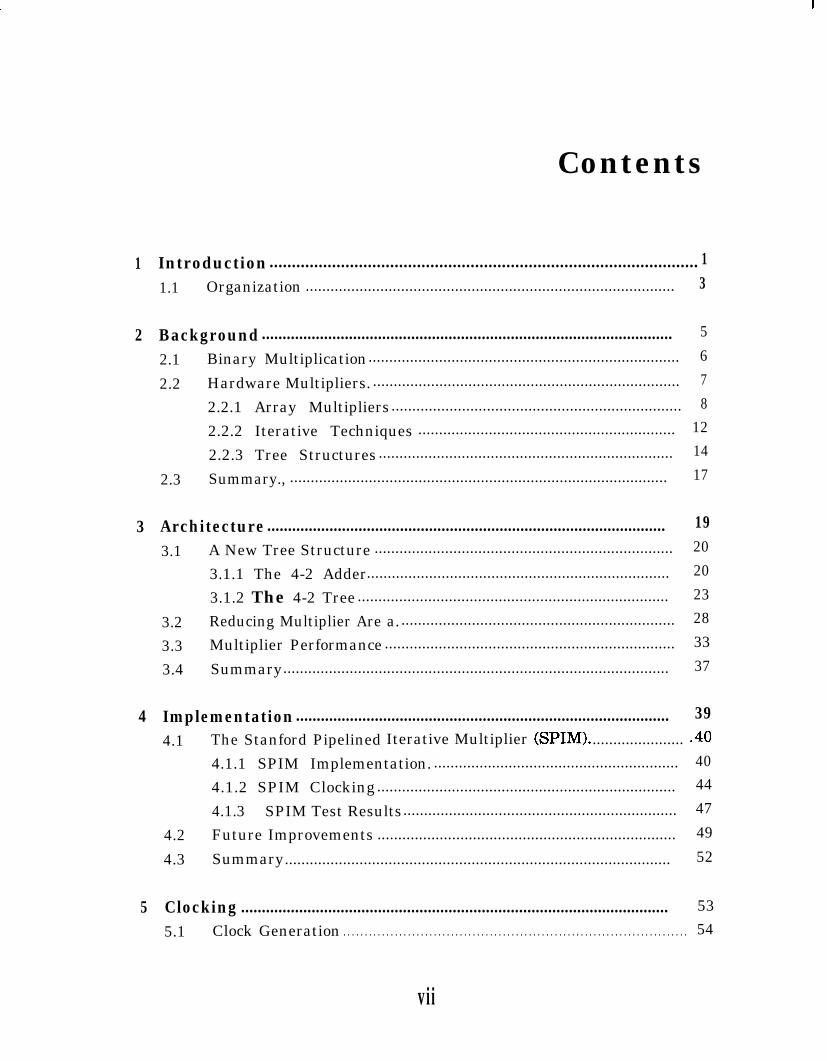
Contents
1
2
3
4
5
Introduction ................................................................................................ 11.1 Organization ......................................................................................... 3
Background ................................................................................................... 5
2.1 Binary Multiplication........................................................................... 6
2.2 Hardware Multipliers. .......................................................................... 7
2.2.1 Array Multipliers...................................................................... 8
2.2.2 Iterative Techniques .............................................................. 12
2.2.3 Tree Structures ....................................................................... 14
2.3 Summary., ........................................................................................... 17
Architecture ................................................................................................ 193.1 A New Tree Structure ........................................................................ 20
3.1.1 The 4-2 Adder......................................................................... 203.1.2 The 4-2 Tree ........................................................................... 23
3.2 Reducing Multiplier Are a. .................................................................. 28
3.3 Multiplier Performance ...................................................................... 33
3.4 Summary............................................................................................. 37
Implementation .......................................................................................... 394.1 The Stanford Pipelined Iterative Multiplier (SPIM). ...................... .40
4.1.1 SPIM Implementation. ........................................................... 404.1.2 SPIM Clocking ........................................................................ 444.1.3 SPIM Test Results.................................................................. 47
4.2 Future Improvements ........................................................................ 494.3 Summary............................................................................................. 52
Clocking ....................................................................................................... 535.1 Clock Generation . . . . . . . . . . . . . . . . . . . . . . . . . . . . . . . . . . . . . . . . . . . . . . . . . . . . . . . . . . . . . . . . . . . . . . . . . . . . . . . . 54
vii
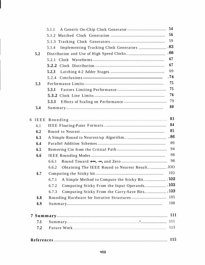
5.2
5.3
5.4
5.1.1 A Generic On-Chip Clock Generator..................................... 545.1.2 Matched Clock Generation .................................................... 565.1.3 Tracking Clock Generators .................................................... 595.1.4 Implementing Tracking Clock Generators .......................... .63Distribution and Use of High Speed Clocks.. ................................... .665.2.1 Clock Waveforms .................................................................... 675.2.2 Clock Distribution .................................................................. 675.2.3 Latching 4-2 Adder Stages. ................................................... 695.2.4 Conclusions ............................................................................ .74Performance Limits............................................................................ 755.3.1 Factors Limiting Performance............................................... 755.3.2 Clock Line Limits ................................................................... 765.3.3 Effects of Scaling on Performance ......................................... 79
Summary............................................................................................. 80
6 IEEE Rounding . . . . . . . . . . . . . . . . . . . . . . . . . . . . . . . . . . . . . . . . . . . . . . . . . . . . . . . . . . . . . . . . . . . . . . . . . . . . . . . . . . . . . . . . . . 836.16.26.36.46.56.6
6.7
6.86.9
IEEE Floating-Point Formats.. ......................................................... 84Round to Nearest. ............................................................................... 85A Simple Round to Nearest/up Algorithm.. ..................................... .86Parallel Addition Schemes................................................................. 89Removing Cin from the Critical Path................................................ 94IEEE Rounding Modes....................................................................... 986.6.1 Round Toward +w, -00, and Zero ............................................ 986.6.2 Obtaining The IEEE Round to Nearest Result.. ............... .lOOComputing the Sticky bit................................................................. 1026.7.1 A Simple Method to Compute the Sticky Bit.. ................... .1026.7.2 Computing Sticky From the Input Operands.. .................. .1036.7.3 Computing Sticky From the Carry-Save Bits.. .................. .103Rounding Hardware for Iterative Structures ................................. 105Summary........................................................................................... 108
7 Summary. . . . . . . . . . . . . . . . . . . . . . . . . . . . . . . . . . . . . . . . . . . . . . . . . . . . . . . . . . . . . . . . . . . . . . . . . . . . . . . . . . . . . . . . . . . . . . . . . . . . . 1117.1 Summary. . . . . . . . . . . . . . . . . . . . . . . . . . . . . . . . . . . . . . . . . . . . . . . . ..*........................................ 1117.2 Future Work . . . . . . . . . . . . . . . . . . . . . . . . . . . . . . . . . . . . . . . . . . . . . . . . . . . . . . . . . . . . . . . . . . . . . . . . . . . . . . . . . . . . . 113
References . . . . . . . . . . . . . . . . . . . . . . . . . . . . . . . . . . . . . . . . . . . . . . . . . . . . . . . . . . . . . . . . . . . . . . . . . . . . . . . . . . . . . . . . . . . . . . . . . . . . . . . 115
. . .vlll
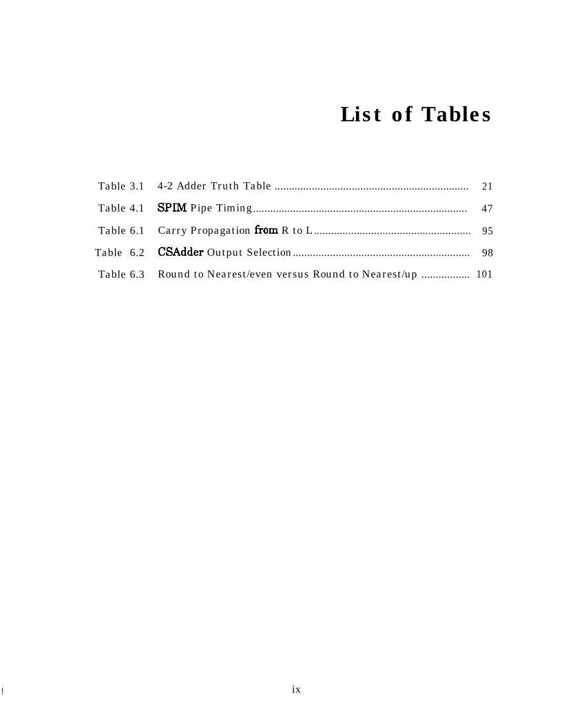
List of Tables
Table 3.1 4-2 Adder Truth Table .................................................................... 21
Table 4.1 SPlM Pipe Timing........................................................................... 47
Table 6.1 Carry Propagation from R to L....................................................... 95
Table 6.2 CSAdder Output Selection.............................................................. 98
Table 6.3 Round to Nearest/even versus Round to Nearest/up ................. 101
ix


List of Figures
Figure 2.1
Figure 2.2
Figure 2.3
Figure 2.4
Figure 2.5
Figure 2.6
Figure 2.7
Figure 3.1
Figure 3.2
Figure 3.3
Figure 3.4
Figure 3.5
Figure 3.6
Figure 3.7
Figure 3.8
Figure 3.9
Figure 3.10
Figure 3.11
Figure 3.12
Figure 3.13
Figure 4.1
Figure 4.2
Basic Multiplication Data Flow.. ................................................... .6
Two Rows of an Array Multiplier.. ................................................ .9
Data Flow Through a Pipelined Array Multiplier.. .................... . l l
Minimal Iterative Structure......................................................... 12
Partial Linear Array ..................................................................... 13
Linear Array versus Tree Structure ............................................ 14
A 6 Input Wallace Tree Slice ........................................................ 16
4-2 Adder Block Diagram ............................................................. 21
4-2 Adder CSA Implementation ................................................... 21
A Row of 4-2 Adders.. ................................................................... 23
An 8 Input 4-2 Tree (Front View). ............................................... .24
An 8 Input 4-2 Tree Slice (Front View). ...................................... 25
Multiple 4-2 Tree Slices Form a 4-2 Multiplier.. ........................ 26
An 8 Bit 4-2 Multiplier Bit Slice Layout.. ................................... 27
A Pipelined 4-2 Tree.. ................................................................... 29
The 4-2 Carry-Save Accumulator.. .............................................. 30
4-2 Tree and Accumulator vs. Partial Linear Array.. ................ .31
An 8 Input Partial 4-2 Tree and 4-2 Accumulator.. .................... .32
Architecture Comparison Plot...................................................... 34
Latency and Throughput vs. Partial Tree Size.. ........................ -36
SPIM Block Diagram .................................................................... 41
SPIM Die Microphotograph.. ....................................................... .43
xi
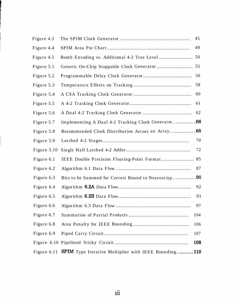
Figure 4.3
Figure 4.4
Figure 4.5
Figure 5.1
Figure 5.2
Figure 5.3
Figure 5.4
Figure 5.5
Figure 5.6
Figure 5.7
Figure 5.8
Figure 5.9
Figure 5.10
Figure 6.1
Figure 6.2
Figure 6.3
Figure 6.4
Figure 6.5
Figure 6.6
Figure 6.7
Figure 6.8
Figure 6.9
The SPIM Clock Generator .......................................................... 45
SPIM Area Pie Chart.................................................................... 49
Booth Encoding vs. Additional 4-2 Tree Level ............................ 50
Generic On-Chip Stoppable Clock Generator.............................. 55
Programmable Delay Clock Generator........................................ 56
Temperature Effects on Tracking ................................................ 58
A CSA Tracking Clock Generator ................................................ 60
A 4-2 Tracking Clock Generator................................................... 61
A Dual 4-2 Tracking Clock Generator ......................................... 62
Implementing A Dual 4-2 Tracking Clock Generator.. .............. .66
Recommended Clock Distribution Across an Array.. ................. .68
Latched 4-2 Stages....................................................................... 70
Single Half Latched 4-2 Adder..................................................... 72
IEEE Double Precision Floating-Point Format........................... 85
Algorithm 6.1 Data Flow .............................................................. 87
Bits to be Summed for Correct Bound to Nearest/up.. ............... .90
Algorithm 6.2A Data Flow............................................................ 92
Algorithm 6.2B Data Flow............................................................ 93
Algorithm 6.3 Data Flow .............................................................. 97
Summation of Partial Products .................................................. 104
Area Penalty for IEEE Bounding............................................... 106
Piped Carry Circuit. .................................................................... 107
Figure 6.10 Pipelined Sticky Circuit ............................................................. 108
Figure 6.11 SPIM Type Iterative Multiplier with IEEE Bounding.. ........... 110
xii

Chapter 1
Introduction
/ ‘
i
The growing market for fast floating-point co-processors, digital signal
processing chips, and graphics processors has created a demand for high-
speed, area-efficient multipliers. Current architectures range from small,
low-performance shift and add multipliers, to large, high-performance array
and tree multipliers. Conventional linear array multipliers achieve high
performance in a regular structure, but require large amounts of silicon. Tree
structures achieve even higher performance than linear arrays but the tree
interconnection is more complex and less regular, making them even larger
than linear arrays. Ideally, one would want the speed benefits of a tree
structure, the regularity of an array multiplier, and the small size of a shift
and add multiplier.
1
Chapter 1. Introduction
This thesis presents a new tree multiplier architecture which is smaller and
faster than linear array multipliers, and more regular than traditional
multiplier trees. At the heart of the architecture is a new tree structure, the
4-2 tree. The regular structure of the 4-2 tree is the result of using a 4-2
adder as the basic building block. A row of 4-2 adders can be used to reduce
four inputs to two outputs. In contrast, the carry-save adders used in
Wallace trees reduce three inputs to two outputs. The 240-1 reduction of the
4-2 adders produces a binary tree structure which is much more regular than
the, 3-to-2 structure found in Wallace trees. As such, 4-2 trees are better
suited for VLSI implementations than traditional multiplier trees.
To reduce the size of the multiplier a partial tree is used together with a 4-2
carry-save accumulator placed at its outputs to iteratively accumulate the
partial products. This allows a full multiplier to be built in a fraction of the
area required by a full array. Higher performance is achieved by increasing
the hardware utilization of the partial 4-2 tree through pipelining. To ensure
optimal performance of the pipelined 4-2 tree, the clock frequency must be
tightly controlled to match the delay of the 4-2 adder pipe stages. To
accomplish this, an on-chip clock generator is proposed which can accurately
match, and track, the delay of the 4-2 multiplier logic. To demonstrate the
feasibility of 4-2 pipelined iterative multipliers a test chip, called SPIM, was
implemented in a 1.6 pm CMOS technology.
Finally, there is more to multiplication than just summing partial products.
To facilitate the construction of fast floating-point multipliers, several new
rounding algorithms, compatible with IEEE standard 754 for binary floating-
point arithmetic, have been developed. While these rounding algorithms are
2
Chapter 1. Introduction
useful for many multiplier architectures, the iterative 4-2 multiplier’s use of a
partial tree means it requires significantly less additional rounding hardware
than full trees, with no performance penalty.
1.1 OrganizationThe next chapter provides background information on the basics of binary
multiplication. The advantages and disadvantages of various hardware
multiplier architectures including linear arrays, trees, and iterative
techniques are discussed.
Chapter 3 introduces a new multiplier architecture consisting of a pipelined
4-2 tree and 4-2 carry-save accumulator. The 4-2 adder, which is the basic
building block used to construct 4-2 trees, is presented. Next, it will be
shown how rows of 4-2 adders can be used to form the regular binary
structure of the 4-2 tree. The advantages of 4-2 trees over traditional
multiplier trees are then discussed. To reduce area, a partial 4-2 tree is
pipelined and used in conjunction with a 4-2 carry-save accumulator. The
performance and size of iterative 4-2 multipliers is then compared to
conventional linear array multipliers, demonstrating the advantages of the
new architecture.
Chapter 4 presents a test chip, the Stanford Pipelined Iterative Multiplier
(SPIM), which was fabricated to demonstrate the feasibility of the new
architecture. SPIM implements the mantissa portion of a double extended
precision (80 bit) floating-point multiply. By using a partial, pipelined 4-2
3
Chapter 1. Introduction
!
tree and accumulator, SPIM provides over twice the performance of a
comparable conventional full array at l/4 of the silicon area. Future
improvements based upon information learned from measurements and
observations on the SPIM chip are then presented.
Chapter 5 discusses the issues involved in clocking high-speed multipliers.
To ensure optimal performance, the 4-2 tree must be clocked at a rate equal
to the combinational delay of the 4-2 stages. To achieve such tight control on
the fast iterative multiplier clock, an on-chip clock generator is proposed that
can accurately match, and track, the delay of the 4-2 multiplier logic.
Techniques for the distribution and use of high-speed multiplier clocks will
then be presented. Finally, performance limits based upon current and
future technologies will be discussed.
Chapter 6 presents several high-performance rounding algorithms that
adhere to IEEE standard 754 for binary floating-point multiplication. It will
then be shown that partial tree iterative multipliers require less additional
rounding hardware than full trees, with no performance penalty.
Finally, Chapter 7 presents a summary of the contributions of this thesis, and
describes directions for future investigations.
4
Chapter 2
Background
Webster’s dictionary defines multiplication as “a mathematical operation that
at its simplest is an abbreviated process of adding an integer to itself a
specified number of times”. A number (multiplicand) is added to itself a
number of times as specified by another number (multiplier) to form a result
(product). In elementary school, students learn to multiply by placing the
multiplicand on top of the multiplier. The multiplicand is then multiplied by
each digit of the multiplier beginning with the rightmost, Least Significant
Digit (LSD). Intermediate results (partial-products) are placed one atop
the other, offset by one digit to align digits of the same weight. The final
product is determined by summation of all the partial-products. Although
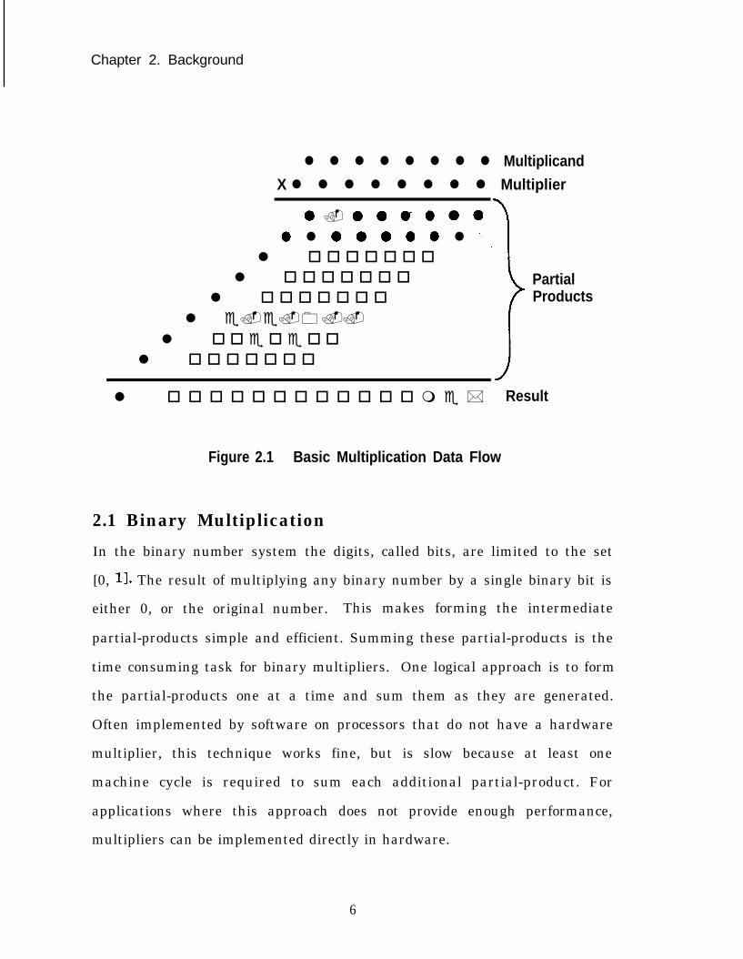
most people think of multiplication only in base 10, this technique applies
equally to any base, including binary. Figure 2.1 shows the data flow for the
basic multiplication technique just described. Each black dot represents a
single digit.
5
Chapter 2. Background
l l l l l l l l MultiplicandX l l l l l l l l Multiplier
l . ..~...0 l 0 0 0 0 0 l 1
l o o o o o o ol o o o o o o o
I
Partiall o o o o o o o Products
l e.e.0..l o o e o e o o
l o o o o o o o
l o o o o o o o o o o o o m e * Result
Figure 2.1 Basic Multiplication Data Flow
2.1 Binary MultiplicationIn the binary number system the digits, called bits, are limited to the set
[0, 11. The result of multiplying any binary number by a single binary bit is
either 0, or the original number. This makes forming the intermediate
partial-products simple and efficient. Summing these partial-products is the
time consuming task for binary multipliers. One logical approach is to form
the partial-products one at a time and sum them as they are generated.
Often implemented by software on processors that do not have a hardware
multiplier, this technique works fine, but is slow because at least one
machine cycle is required to sum each additional partial-product. For
applications where this approach does not provide enough performance,
multipliers can be implemented directly in hardware.
6
Chapter 2. Background
2.2 Hardware MultipliersDirect hardware implementations of shift and add multipliers can increase
performance over software synthesis, but are still quite slow. The reason is
that as each additional partial-product is summed a carry must be
propagated from the least significant bit (lsb) to the most significant bit
(msb). This carry propagation is time consuming, and must be repeated for
each partial product to be summed.
One method to increase multiplier performance is by using encoding
techniques to reduce the the number of partial products to be summed. Just
such a technique was first proposed by Booth [BOO 511. The original Booth’s
algorithm ships over contiguous strings of l’s by using the property that: 2” +
2(n-1) + 2(n-2) + . . . + 2hm) = 2(n+l) - 2(n-m). Although Booth’s algorithm
produces at most N/2 encoded partial products from an N bit operand, the
number of partial products produced varies. This has caused designers to use
modified versions of Booth’s algorithm for hardware multipliers. Modified 2
bit Booth encoding halves the number of partial products to be summed.
Since the resulting encoded partial-products can then be summed using any
suitable method, modified 2 bit Booth encoding is used on most modern
floating-point chips [LU 881, [MCA 861. A few designers have even turned to
modified 3 bit Booth encoding, which reduces the number of partial products
to be summed by a factor of three IBEN 891. The problem with 3 bit encoding
is that the carry-propagate addition required to form the 3X multiples often
overshadows the potential gains of 3 bit Booth encoding.
7
Chapter 2. Background
To achieve even higher performance, advanced hardware multiplier
architectures search for faster and more efficient methods for summing the
partial-products. Most increase performance by eliminating the time
consuming carry propagate additions. To accomplish this, they sum the
partial-products in a redundant number representation. The advantage of a
redundant representation is that two numbers, or partial-products, can be
added together without propagating a carry across the entire width of the
number. Many redundant number representations are possible. One
commonly used representation is known as carry-save form. In this
redundant representation two bits, known as the carry and sum, are used to
represent each bit position. When two numbers in carry-save form are added
together any carries that result are never propagated more than one bit
position. This makes adding two numbers in carry-save form much faster
than adding two normal binary numbers where a carry may propagate. One
common method that has been developed for summing rows of partial
products using a carry-save representation is the array multiplier.
2.2.1 Array Multipliers
Conventional linear array multipliers consist of rows of carry-save adders
(CSAj.1 A port’ion of an array multiplier with the associated routing can be
seen in Figure 2.2. In a linear array multiplier, as the data propagates down
through the array, each row of CSA’s adds one additional partial-product to
the partial sum. Since the intermediate partial sum is kept in a redundant,
lC!any save adders are also often referred to as full adders or 3-2 counters. Each CSA takesin three inputs of the same weight and produces two outputs, a sum of weight 1 and a carryof weight 2.
8

Chapter 2. Background
carry-save form there is no carry propagation. This means that the delay of
an array multiplier is only dependent upon the depth of the array, and is
independent of the partial-product width. Linear array multipliers are also
regular, consisting of replicated rows of CSA’s. Their high performance and
regular structure have perpetuated the use of array multipliers for VLSI
math co-processors and special purpose DSP chips, for example WAR 821.
II II II .L-.L-
7t7t 7777 7777A B C A B CA BC A BC
trytryA B C A B CA B C A B C
CSACSA CSACSA CSACSA CSACSACarry Sum Carry Sum Carry Sum Carry Sum
I 1 I I I I I
Carry Sum 1 Carry Sum I Carry Sum I Carry Sum
CSA CSA CSA CSACarry Sum Carry Sum Carry Sum Carry Sum
1 I I
Figure 2.2 Two Rows of an Array Multiplier*
The biggest problem with full linear array multipliers is that they are very
large. As operand sizes increase, linear arrays grow in size at a rate equal to
2The large black dots represent the bits of the partial products to be summed. The partialproducts can be formed by any of several methods including: a logical AND of the multiplierand multiplicand bits, or by Booth encoding.
9

Chapter 2. Background
the square of the operand size. This is because the number of rows in the
array is equal to the length of the multiplier, with the width of each row
equal to the width of multiplicand. The large size of full arrays typically
prohibits their use, except for small operand sizes, or on special purpose math
chips where a major portion of the silicon area can be assigned to the
multiplier array.
Another problem with array multipliers is that the hardware is underutilized.
As the sum is propagated down through the array, each row of CSA’s
computes a result only once, when the active computation front passes that
row. Thus, the hardware is doing useful work only a very small percentage of
the time. This low hardware utilization in conventional linear array
multipliers makes performance gains possible through increased efficiency.
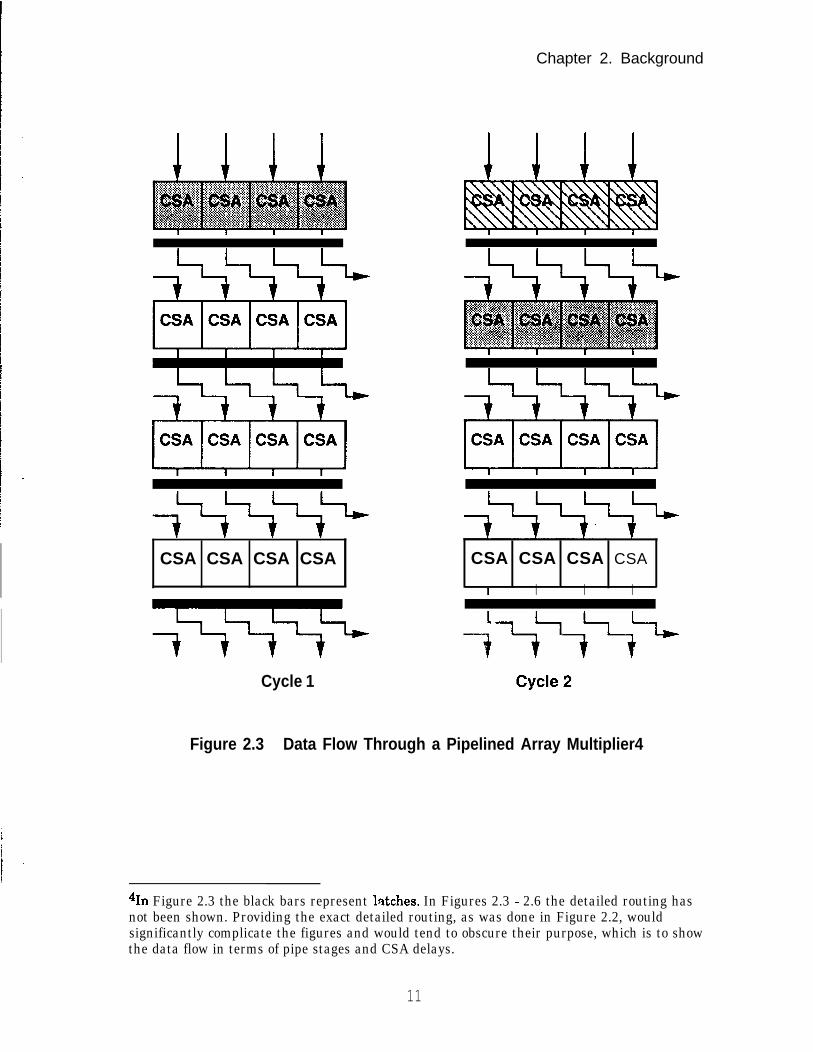
For example, by overlapping calculations pipelining can achieve a large gain
in throughput [NOL 861. Figure 2.3 shows a full array pipelined after each
row of CSA’s. Once the partial sum has passed the first row of CSA’s,
represented by the shaded row of GSA’s in cycle 1, a subsequent multiply can
be started on the next cycle. In cycle 2, the first partial sum has passed to the
second row of CM’s, and the second multiply, represented by the cross
hatched row of CSA’s, has begun. Although pipelining a full array can
greatly increase throughput, both the size and latency are increased due to
the additional latches .s While high throughput is desirable, for general
purpose computers size and latency tend to be more important; thus, fully
pipelined linear array multipliers are seldom found.
3Adding latches after each row of C&i’s, as in Figure 2.3, typically increases both the sizeand latency from 30 to 50 96. Due to the large latch overhead, more than one row of CM’s isusually placed between latches.
10
Chapter 2. Background
CSA CSA CSA CSA CSA CSA CSA CSA
I I I I
Cycle 1
Figure 2.3 Data Flow Through a Pipelined Array Multiplier4
41n Figure 2.3 the black bars represent latches. In Figures 2.3 - 2.6 the detailed routing hasnot been shown. Providing the exact detailed routing, as was done in Figure 2.2, wouldsignificantly complicate the figures and would tend to obscure their purpose, which is to showthe data flow in terms of pipe stages and CSA delays.
11

Chapter 2. Background
2.2.2 Iterative Techniques
To reduce area, some designers use partial arrays and iterate using a clock.
At the limit, a minimal iterative structure would have one row of CSA’s and a
latch (see Figure 2.4).5 Clearly, this structure requires the least amount of
hardware, and has the highest utilization since each CSA is used every cycle.
An important observation is that iterative structures are fast if the latch
delays are small, and the clock is matched to the combinational delay of the
CSA’s. If both of these conditions are met, iterative structures approach the
same throughput and latency as full arrays. The only difference in latency is
due to the latch and clock overhead. Although they require very fast clocks, a
few companies use iterative structures in their new high-performance floating
point processors [ELK 871.
CSA CSA CSA CSA
Figure 2.4 Minimal Iterative Structure
51n fact, one rarely finds a multiplier array that consists of only a single row of CSA’s. Likethe pipelined linear array, the latch overhead with only a single row of CM’s between latchesis extremely high.
12
Chapter 2. Background
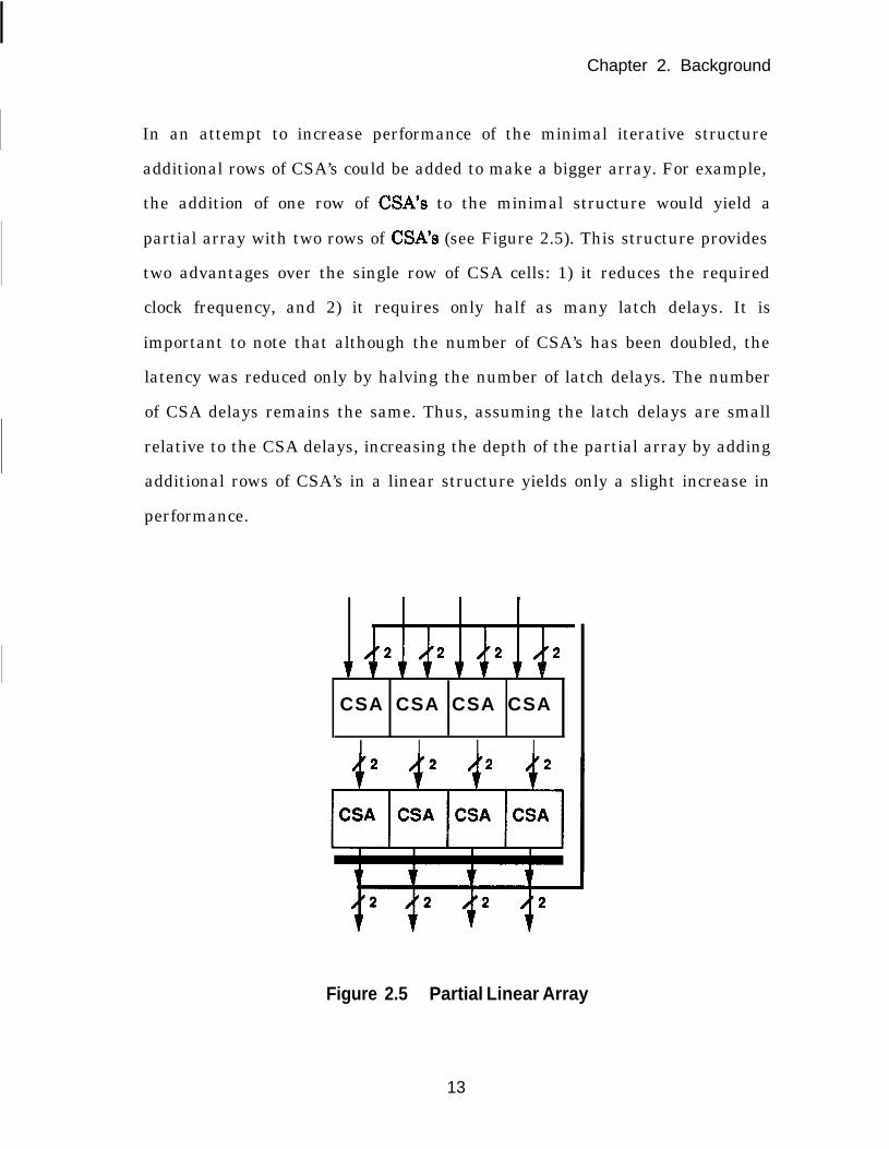
In an attempt to increase performance of the minimal iterative structure
additional rows of CSA’s could be added to make a bigger array. For example,
the addition of one row of CM’s to the minimal structure would yield a
partial array with two rows of CM’s (see Figure 2.5). This structure provides
two advantages over the single row of CSA cells: 1) it reduces the required
clock frequency, and 2) it requires only half as many latch delays. It is
important to note that although the number of CSA’s has been doubled, the
latency was reduced only by halving the number of latch delays. The number
of CSA delays remains the same. Thus, assuming the latch delays are small
relative to the CSA delays, increasing the depth of the partial array by adding
additional rows of CSA’s in a linear structure yields only a slight increase in
performance.
‘ICSA CSA CSA CSA
I I I I
Figure 2.5 Partial Linear Array
13

Chapter 2. Background
To achieve additional increases in performance one obvious step is to make
the CM’s faster. Another powerful technique for increasing performance is
to reduce the number of series additions required to sum the partial-products
by using tree structures.
2.23 Tree Structures
Trees are an extremely fast structure for summing partial-products. In a
linear array, each row sums one additional partial product. As such, linear
arrays require order N stages to reduce N partial-products. In contrast, by
doing the additions in parallel, tree structures require only order log N stages
to reduce N partial products (see Figure 2.6).
t
Binary TreeDepth 01 IogN
Figure 2.6 Linear Array versus Tree Structure
14
Chapter 2. Background
Although trees are faster than linear arrays they still require one row of
CSA’s for each partial-product to be summed, making them large. Additional
wiring required to gather bits of the same weight makes trees even larger
than linear arrays. The additional wiring required of full trees over linear
arrays has caused designers to look at permutations of the basic tree
structure to ease the routing [ZUR 861. Unbalanced or modified trees make a
compromise between conventional full arrays and full tree structures. They
reduce the routing required of full trees, while slightly increasing the
serialization of the partial-product summations.
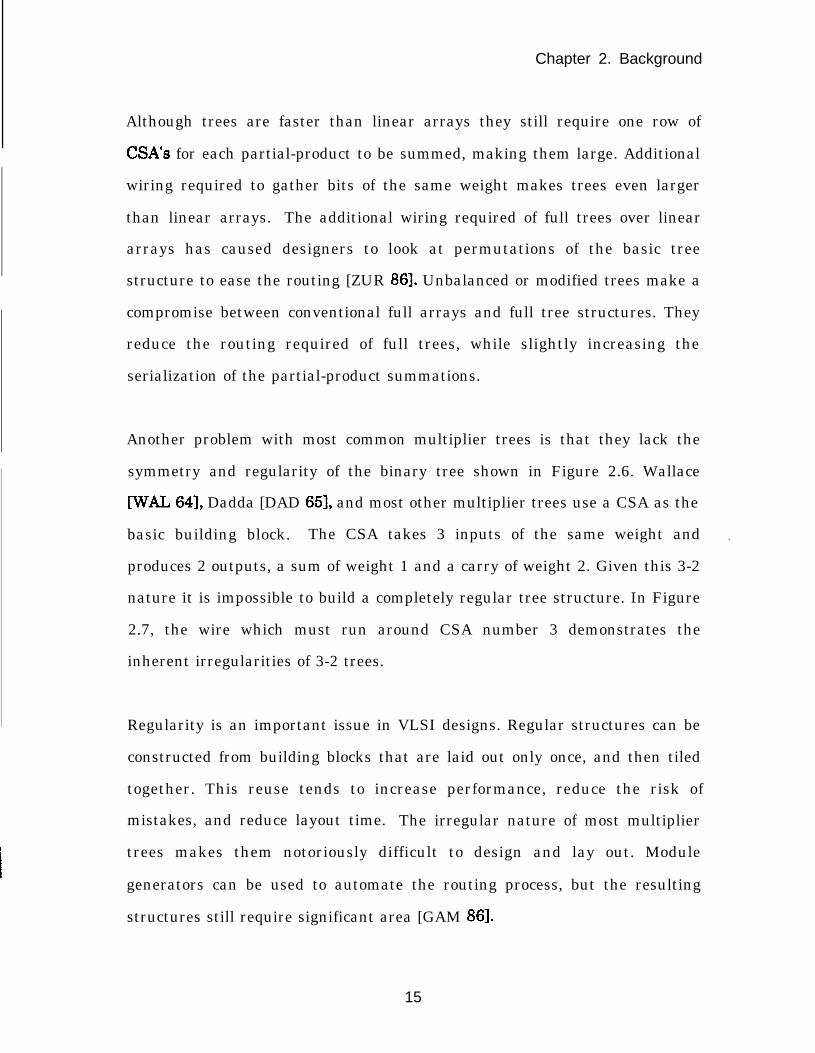
Another problem with most common multiplier trees is that they lack the
symmetry and regularity of the binary tree shown in Figure 2.6. Wallace
[WAL 641, Dadda [DAD 651, and most other multiplier trees use a CSA as the
basic building block. The CSA takes 3 inputs of the same weight and .
produces 2 outputs, a sum of weight 1 and a carry of weight 2. Given this 3-2
nature it is impossible to build a completely regular tree structure. In Figure
2.7, the wire which must run around CSA number 3 demonstrates the
inherent irregularities of 3-2 trees.
Regularity is an important issue in VLSI designs. Regular structures can be
constructed from building blocks that are laid out only once, and then tiled
together. This reuse tends to increase performance, reduce the risk of
mistakes, and reduce layout time. The irregular nature of most multiplier
trees makes them notoriously difficult to design and lay out. Module
generators can be used to automate the routing process, but the resulting
structures still require significant area [GAM 861.
15
Chapter 2. Background
PCSA CSAL2CI
csCl+1
TJclI’ ’ LI CSA
4cs
b-
Figure 2.7 A 6 Input Wallace Tree Slice
To produce a more regular tree structure, multipliers based upon redundant
representations other than carry-save form have been presented [HAR 871.
In an attempt to reduce both the size and complexity of the wiring, one
architecture uses a radix 4 redundant form to produce a binary like tree, then
encodes the signals using multiple-valued logic to reduce wire
interconnections [RAW 881. To reduce wiring, the DEC MultiTitan multiplier
uses higher order counters which reduce the partial products more rapidly
than the 3-2 reduction factor found in Wallace trees [JOU 881. The higher
order counters perform a 2-to-1 compression to achieve a binary tree
structure. To reduce area, the MultiTitan multiplier uses a half tree which is
“double pumped” on alternate phases of the system clock.
16

Chapter 2. Background
No matter which type of tree structure is used, full trees are big. One method
to reduce tree size is to use a partial tree and iteratively accumulate the
partial products. This technique was first used on the IBM 360 Model 91
floating point unit which uses a partial 3-2 tree, and then iteratively
accumulates the partial products using a carry-save accumulator [AND 671.
One problem with the Model 91 architecture is that the 3-2 tree structure is
not regular. In addition, the fast iterative clocks require tight control over
pipe stage delays. The irregular tree structure, combined with the fact that
the multiplier was implemented at the board level, made signal routing and
balancing the separate pipe stages difficult. Still, the Model 91 multiplier
demonstrated the advantages of partial iterative trees. The next chapter will
demonstrate how the advantages of partial iterative trees can be applied to a
regular tree structure, which is integrated on a single VLSI chip, to provide
the performance advantages of trees in a smaller, more regular structure.
2.3 SummaryVirtually all high-performance multipliers use a redundant number
representation to eliminate intermediate carry propagate additions when
summing partial products. Array multipliers are fast and regular, and, as
such, are well suited for VLSI implementations. Trees have even higher
performance, but the lack of a regular structure makes them difficult to
design and lay out. Regular tree structures can improve layout density,
increase performance, and reduce layout time. Ideally, one would want the
performance benefits of trees in a small, regular structure. An architecture
which provides these benefits will be discussed in the next chapter.
17


Chapter 3
Architecture
The last chapter showed that tree structures are an extremely fast method for
summing partial products. Though fast, most commonly used multiplier
trees are very large, and irregular. This chapter introduces a new tree
structure, the 4-2 tree, which is similar to a binary tree in nature, and, is
therefore, both symmetric and regular. It will then be shown that pipelining
a partial 4-2 tree and iteratively accumulating the resulting partial products
can provide the performance advantages of trees in a significantly smaller
size. The result is a flexible multiplier architecture in which the partial tree
size can be adjusted to meet area and performance constraints.
19
Chapter 3. Architecture
3.1 A New Tree StructureThe 2-to-1 nature of binary trees makes them symmetric and regular. The
fact is, any basic building block which reduces partial products by a factor of
two will yield a regular and symmetric tree. The most basic 2-to-1 reduction,
reducing two binary numbers to one, requires a carry propagate adder.
Although a regular structure would result, the long carry propagation time
makes this structure too slow to be useful in a high-performance multiplier
core. A redundant number representation can be used to overcome the carry
propagation problem; however, numbers in carry-save form require two bits
to represent each single bit position. As a result, reducing two carry-save
numbers to one carry-save number requires an adder which takes in four
inputs and sums them to produce two outputs. This redundant binary adder
can be efficiently constructed from a basic building block known as the 4-2
adder. Using 4-2 adders a new tree structure, the 4-2 tree, can be
constructed. The redundant number representation makes the 4-2 tree fast,
and, because it is a binary tree, it is also symmetric and regular.
3.1.1 The 4-2 Adder
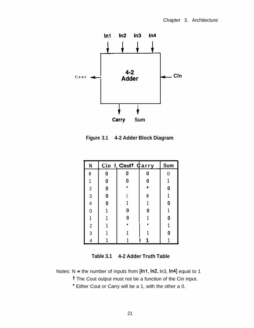
Figure 3.1 is a block diagram of the 4-2 adder. The corresponding 4-2 adder
truth table is shown in Table 3.1.
20
Chapter 3. Architecture
In1 In2 In3 In4
C o u t e4-2
Adder J Cln
I It t
Carry Sum
Figure 3.1 4-2 Adder Block Diagram
N Cin I C_ __ _0 01 02 03 04 00 11 12 13 14 1
Joutt C a r r y0 00 0l 4
1 01 10 00 1l l
1 11 I 1
Sum0101010101
Table 3.1 4-2 Adder Truth Table
Notes: N = the number of inputs from [Inl, ln2, ln3, In41 equal to 1t The Cout output must not be a function of the Cin input.* Either Cout or Carry will be a 1, with the other a 0.
21

Chapter 3. Architecture
The 4-2 adder has occasionally been implemented, either intentionally or
coincidentally, using two CSA’s in series (see Figure 3.2). This configuration
is not optimal, but is quite efficient. 6 Although implementing a 4-2 adder
directly from its truth table can produce a faster structure, few attempts have
been made at direct 4-2 adder implementations, with one exception [SHE 781.
In1 In2 In3 In4
Cout
7 ,CSA
c s4 J
7CSA
, c S
Cin
Carry Sum
Figure 3.2 4-2 Adder CSA Implementation
Although the 4-2 adder actually has five inputs and three outputs, the name
is derived from the fact that a row of 4-2 adders reduces 4 numbers to 2 (see
Figure 3.3). The name also serves to distinguish the 4-2 adder from a 5-3
counter. Both the 4-2 adder and 5-3 counter take in 5 inputs of the same
61mplementing the 4-2 adder with two CSA’s is also useful as a metric for comparisons toother architectures. In this dissertation comparisons with other architectures are often madebased on CSA delays. This provides a fair comparison since it is both technology and circuitindependent.
22
Chapter 3. Architecture
weight; however, a 5-3 counter produces 3 outputs of different weights, while
the 4-2 adder produces a sum of weight 1 and two carries of weight 2. Also,
the Cout output of a 4-2 adder must not be a function of the Cin input, or a
ripple carry could occur when using a row of 4-2 adders to construct a
redundant binary adder.
In1 in2 In3 In4 In1 In2 In3 In4 In1 In2 In3 In4 In1 In2 In3 In4
4-2 4-2 4-2 4-2-cold Cln * Cout Cln * Cout Cln * Cout Cln W-
Carry S u m Carry S u m Carry Sum Carry Sum
4 I
Figure 3.3 A Row of 4-2 Adders
3.1.2 The 4-2 Tree
The 4-2 adder is the basic building block used to construct 4-2 trees. An
example of an 8 by 8 bit 4-2 tree is shown in Figure 3.4. Three 8 bit deep
rows of 4-2 adders are used to form the 4-2 tree. In the 4-2 tree, for every
four inputs taken in at one level, two outputs are produced at the next lower
level. Since each level of the the 4-2 tree reduces two redundant numbers to
one redundant number the 4-2 tree can also be viewed as a redundant binary
tree. Its binary nature makes the 4-2 tree regular, and as such better suited
for VLSI implementations than 3-2 trees.
23

Chapter 3. Architecture
u-u8 8 8 8
8 bit deeprow of 4-2
Adders
u-i-i8 8 8 8
8 bit deeprow of 4-2
Adders
Figure 3.4 An 8 Input 4-2 Tree (Front View)
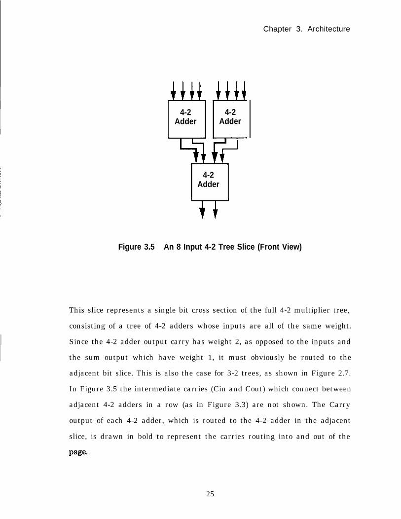
To simplify the diagrams, typically only a single slice of the complete
multiplier tree is shown. The slice is taken at one bit position where all of the
inputs to the adders are of the same weight. An example is the Wallace tree
slice that was shown in Figure 2.7. To form the complete multiplier at least
one tree slice is required for each operand bit, with the intermediate carries
communicating between adjacent slices. A single 4-2 adder wide slice of the
4-2 tree is shown in Figure 3.5.
24
Chapter 3. Architecture
4-2 4-2Adder Adder
4-2Adder
Figure 3.5 An 8 Input 4-2 Tree Slice (Front View)
This slice represents a single bit cross section of the full 4-2 multiplier tree,
consisting of a tree of 4-2 adders whose inputs are all of the same weight.
Since the 4-2 adder output carry has weight 2, as opposed to the inputs and
the sum output which have weight 1, it must obviously be routed to the
adjacent bit slice. This is also the case for 3-2 trees, as shown in Figure 2.7.
In Figure 3.5 the intermediate carries (Cin and Cout) which connect between
adjacent 4-2 adders in a row (as in Figure 3.3) are not shown. The Carry
output of each 4-2 adder, which is routed to the 4-2 adder in the adjacent
slice, is drawn in bold to represent the carries routing into and out of the
page.
25
Chapter 3. Architecture
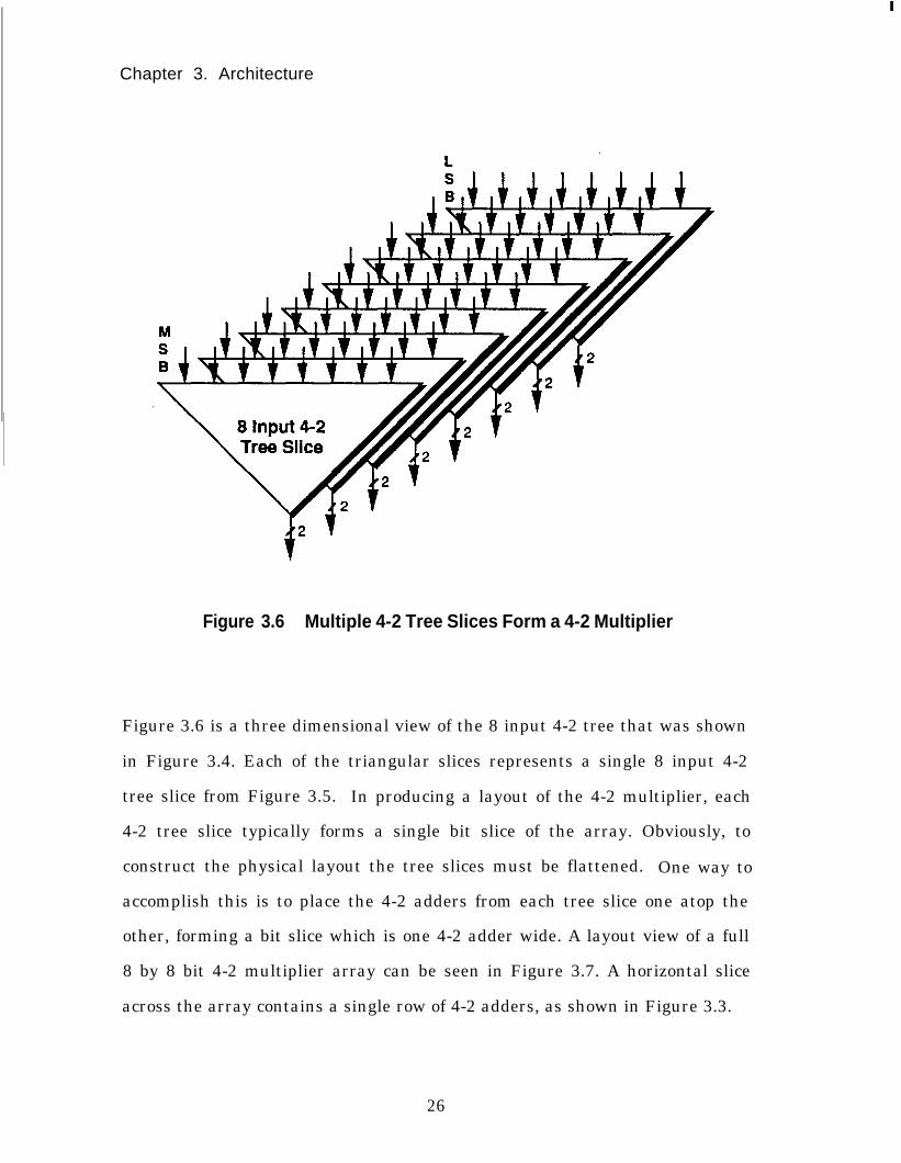
Figure 3.6 Multiple 4-2 Tree Slices Form a 4-2 Multiplier
Figure 3.6 is a three dimensional view of the 8 input 4-2 tree that was shown
in Figure 3.4. Each of the triangular slices represents a single 8 input 4-2
tree slice from Figure 3.5. In producing a layout of the 4-2 multiplier, each
4-2 tree slice typically forms a single bit slice of the array. Obviously, to
construct the physical layout the tree slices must be flattened. One way to
accomplish this is to place the 4-2 adders from each tree slice one atop the
other, forming a bit slice which is one 4-2 adder wide. A layout view of a full
8 by 8 bit 4-2 multiplier array can be seen in Figure 3.7. A horizontal slice
across the array contains a single row of 4-2 adders, as shown in Figure 3.3.
26

Chapter 3. Architecture
FlrstTreeLevel
(2 row
SecondTreeLevel
(1 rw
4-2 4-2 4-2 4-2
SlngleRow of
4-2Adders
4-2 TreeSlice
Figure 3.7 An 8 Bit 4-2 Multiplier Bit Slice Layout
Like all trees the 4-2 tree is fast. A 4-2 tree sums N partial products in
logz(N/2) 4-2 stages, whereas a Wallace tree requires logl.a(N/2) 3-2 stages.
Though the 4-2 tree might appear faster than the Wallace tree, the basic 4-2
cell is more complex than a single CSA, so the speeds are comparable. The
regularity of 4-2 trees over 3-2 trees does, however, tend to contribute to
increased performance. One reason is that regular structures have
predictable wire lengths. This means that buffers can be more easily, and
accurately, tuned to match the wire loads.
Another advantage of 4-2 trees over 3-2 trees is that they can be more easily
pipelined. This is partially due to the more regular structure. Pipelining a
4-2 tree is a simple matter of adding a latch after each 4-2 adder. Pipelining
provides maximum throughput with only a small increase in latency, which is
caused by the additional latches. In the next section it will be shown how
27
Chapter 3. Architecture
pipelining can also be important in reducing the size of the multiplier while
still achieving high performance.
3.2 Reducing Multiplier Area
Wallace trees and linear arrays both require approximately one CSA for each
partial product to be reduced. Similarly, 4-2 trees require one 4-2 adder for
every two partial products. Thus, like the other structures, 4-2 trees are
large. One solution to the size problem is to use a partial 4-2 tree. As an
example, a 64 bit operand could be multiplied in four pieces using a 16 X 64
bit partial 4-2 tree. The four partial results are then summed to form the
complete result. One performance limiting factor of this method is the
latency through the 4-2 tree. The first 16 X 64 bit partial multiply must flow
through the entire 4-2 tree before the next partial multiply can be started
down the array.
The solution to the latency problem lies with better hardware utilization.
Just as the pipelined linear array greatly increases throughput by increasing
utilization, pipelining a 4-2 tree after each level of 4-2 adders greatly
increases its throughput (see Figure 3.8). Although the latency for the first
partial multiply through the tree would be slightly longer due to the added
latches, subsequent partial results arrive on each 4-2 cycle thereafter. The
result is that much less time is required to generate all of the partial results.
As an example, the pipelined 16 X 64 tree shown in Figure 3.8 would require
6 cycles to generate all four 16 X 64 bit partial results, where each cycle
consists of a 4-2 adder and a latch. In contrast, a 16 X 64 tree which is not
28

Chapter 3. Architecture
pipelined would require 12 4-2 adder delays. Assuming the latch delays are
small relative to the 4-2 adder delays, the pipelined structure would be about
twice as fast.
4-2Adder
I I
4-2Adder
4-2Adder
4-2Adder
4-2 4-2Adder Adder
I I I I
4-2Adder
Figure 3.8 A Pipelined 4-2 Tree
The problem with generating the partial results at such a fast rate is that the
accumulator needs to operate at the same frequency as the pipelined 4-2
adder stages, so it can sum the partial products as they are generated. A
carry propagate adder is clearly too slow, but a 4-2 carry-save accumulator
can operate at this rate.
29
Chapter 3. Architecture
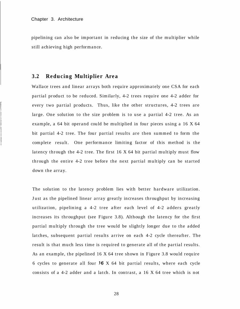
The 4-2 carry-save accumulator is constructed from a row of latched 4-2
adders. Two of the 4-2 adder inputs are used to sum the previously latched
outputs, while the other two inputs are used for the new partial sum. Since
each partial sum generated by the partial 4-2 tree is more significant than the
previous partial sum, the latched accumulator outputs must be shifted to
align with the new partial sum. For example, an 8 input partial 4-2 tree
requires an 8 bit shift in the accumulator to align bits of the same weight.
Figure 3.9 shows a 4 bit 4-2 carry-save accumulator.
shift
Figure 3.9 The 4-2 Carry-Save Accumlator
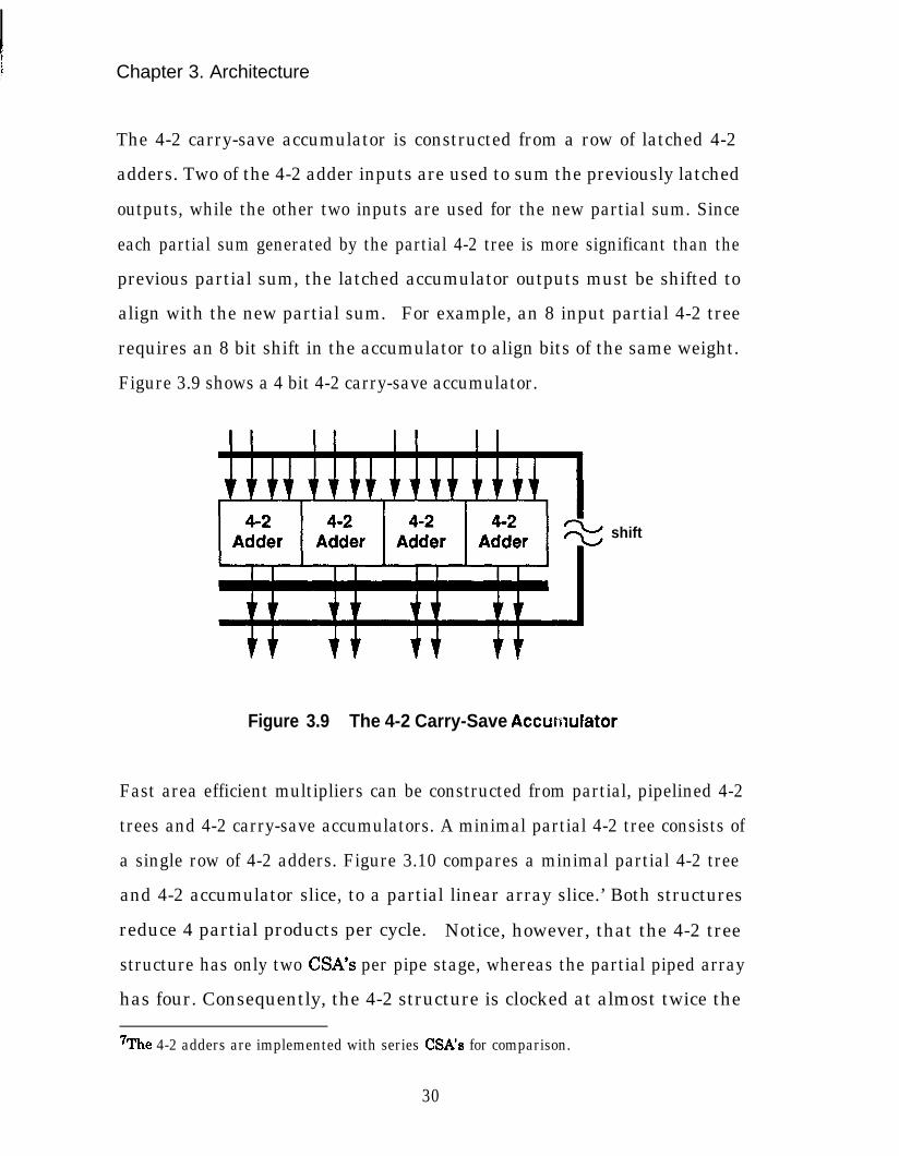
Fast area efficient multipliers can be constructed from partial, pipelined 4-2
trees and 4-2 carry-save accumulators. A minimal partial 4-2 tree consists of
a single row of 4-2 adders. Figure 3.10 compares a minimal partial 4-2 tree
and 4-2 accumulator slice, to a partial linear array slice.’ Both structures
reduce 4 partial products per cycle. Notice, however, that the 4-2 tree
structure has only two CSA’s per pipe stage, whereas the partial piped array
has four. Consequently, the 4-2 structure is clocked at almost twice the
‘The 4-2 adders are implemented with series CSA’s for comparison.
30

Chapter 3. Architecture
frequency of the partial piped array. The result is a much faster multiply.
For example, to reduce 32 partial products the partial linear array would
require 8 cycles, for a total of 32 CSA delays. In contrast, the partial 4-2 tree
would require 9 4-2 cycles, one cycle to pass through the 4-2 tree and 8 cycles
to accumulate the 32 partial products, for a total of 18 CSA delays. Thus, the
4-2 adder and accumulator is almost twice as fast as the partial piped array,
while using roughly the same amount of hardware.
4-2Carry-Save
Accumulator
CSA
I I
Y-3CSA
75CSA
Figure 3.10 4-2 Tree and Accumulator vs. Partial Linear Array
31
Chapter 3. Architecture
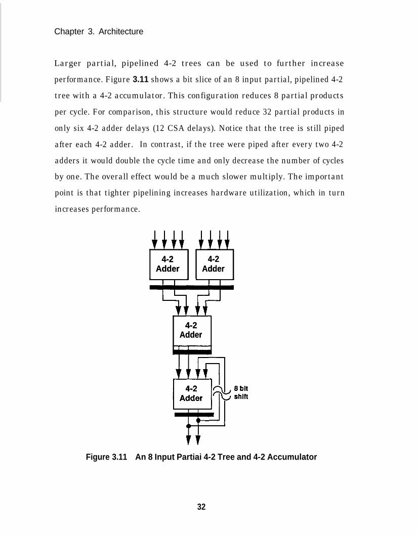
Larger partial, pipelined 4-2 trees can be used to further increase
performance. Figure 3.11 shows a bit slice of an 8 input partial, pipelined 4-2
tree with a 4-2 accumulator. This configuration reduces 8 partial products
per cycle. For comparison, this structure would reduce 32 partial products in
only six 4-2 adder delays (12 CSA delays). Notice that the tree is still piped
after each 4-2 adder. In contrast, if the tree were piped after every two 4-2
adders it would double the cycle time and only decrease the number of cycles
by one. The overall effect would be a much slower multiply. The important
point is that tighter pipelining increases hardware utilization, which in turn
increases performance.
4-24-2 4-24-2AdderAdder AdderAdder
4-24-2AdderAdder
Figure 3.11 An 8 Input Partiai 4-2 Tree and 4-2 Accumulator
32
Chapter 3. Architecture
3.3 Multiplier PerformanceThere are two important metrics of multiplier performance, latency and
throughput. Latency is usually more important in most general purpose
multiplier applications, though throughput is important for applications such
as digital signal processing. In a conventional array multiplier the latency is
linearly proportional to the number of partial products to be reduced. In
other words, a linear array requires N CSA delays to reduce N partial
products. In contrast, the latency of the partial, pipelined 4-2 tree multiplier
is equal to the depth of the partial 4-2 tree plus the number of cycles needed
to accumulate the complete product. As previously stated, the depth of a K
bit 4-2 tree is loga(W2) cycles. Given a K bit partial tree, K partial products
would be summed by the accumulator each cycle. Thus a total of N/K cycles
would be required to accumulate the full N partial products. To summarize,
given a K bit partial 4-2 tree, the number of 4-2 cycles latency required for a
4-2 multiplier to reduce N partial products would be:
Latenw4.2 cycles) = logs(KI2) + (N/K) (3.1)
Like the linear array, a partial 4-2 tree which reduces K partial products per
cycle requires K CM’s per bit-slice (K/2 4-2 adders). The cycle time of the 4-2
structure is, of course, much less, resulting in much higher performance for
the 4-2 multiplier. Notice that although a partial tree is used in place of a
full tree, the logarithmic nature of the tree structure still makes the partial
4-2 tree multiplier much faster than a conventional linear array of the same
size. The size and speed advantages of different sized partial, pipelined 4-2
33

Chapter 3. Architecture
trees with 4-2 accumulators over conventional linear arrays can be seen in
Figure 3.12.
It4 Array n Full Array
4 input Plped tree
8 Input Piped tree
n Conventionalpartial arraystructures
‘I Piped partialtree structures I
vm-7 Full Tree
I
l/4
I
l/2
I
314
I wi Size
(CSA celW32)
Figure 3.12 Architecture Comparison Plot8
8ThF plot assumes 32 rrtial products are to be reduced. Latency is in terms of CSA delays,and mcludes latches w lch have been assumed equivalent to l/3 of a CSA delay. Size is interms of the number of CSA’s, and has been normalized such that 32 rows of CSA’s (a fullarray) has a size of 1 unit. Size does not include latch or wiring area.
34
Chapter 3. Architecture
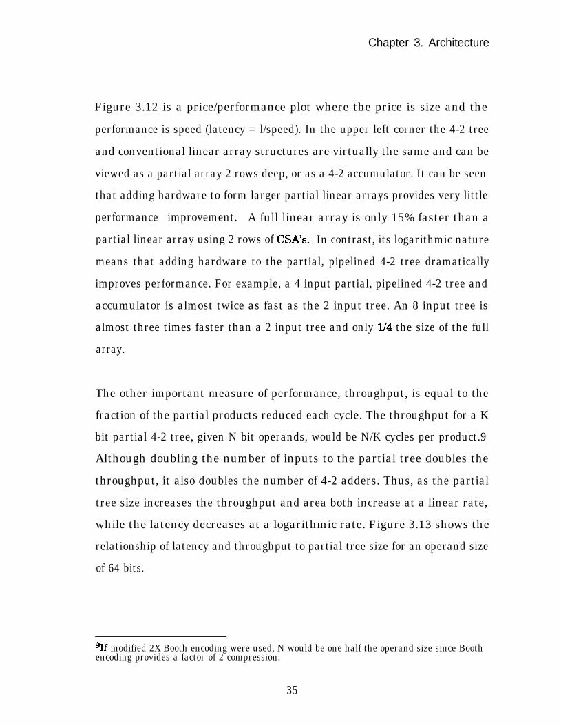
Figure 3.12 is a price/performance plot where the price is size and the
performance is speed (latency = l/speed). In the upper left corner the 4-2 tree
and conventional linear array structures are virtually the same and can be
viewed as a partial array 2 rows deep, or as a 4-2 accumulator. It can be seen
that adding hardware to form larger partial linear arrays provides very little
performance improvement. A full linear array is only 15% faster than a
partial linear array using 2 rows of CSA’s. In contrast, its logarithmic nature
means that adding hardware to the partial, pipelined 4-2 tree dramatically
improves performance. For example, a 4 input partial, pipelined 4-2 tree and
accumulator is almost twice as fast as the 2 input tree. An 8 input tree is
almost three times faster than a 2 input tree and only l/4 the size of the full
array.
The other important measure of performance, throughput, is equal to the
fraction of the partial products reduced each cycle. The throughput for a K
bit partial 4-2 tree, given N bit operands, would be N/K cycles per product.9
Although doubling the number of inputs to the partial tree doubles the
throughput, it also doubles the number of 4-2 adders. Thus, as the partial
tree size increases the throughput and area both increase at a linear rate,
while the latency decreases at a logarithmic rate. Figure 3.13 shows the
relationship of latency and throughput to partial tree size for an operand size
of 64 bits.
gIf modified 2X Booth encoding were used, N would be one half the operand size since Boothencoding provides a factor of 2 compression.
35

Chapter 3. Architecture
70 Q
60 & &
1.00
& 0.90&
Latency && o-8’
(CSA’S) 50 & 1
Throughput#A.
0.70 (Mpykycle)
-I 0.60
-' 0.50
-' 0.40
-' 0.30
10 --*&-- -* 0.10&
0 -@ I I I I I I I 0 . 0 0
1 8 16 24 32 40 48 56 64Partial Tree Size (Inputs)
Figure 3.13 Latency and Throughput vs. Partial Tree Size
While a full, pipelined 4-2 tree achieves a maximum throughput of one
multiply per 4-2 cycle, it is very large. Thus, a full 4-2 tree should only be
used when maximum throughput is required. When latency and area are the
deciding factors, smaller trees should be used. The latency for an N/4 sized
partial tree is only 2 cycles slower than that of a full tree of size N, while only
l/4 the size. The throughput is, of course, reduced by a factor of four. As an
example, a 16 input partial 4-2 tree would reduce 64 partial products in 7
cycles, compared to 5 cycles for a full 64 bit tree. Thus, the four fold increase
in area incurred by the full tree would provide only a 29 8 decrease in
latency. In addition, as the tree size increases the maximum wire length
increases. The longer wires tend to increase the cycle time, decreasing the
36

Chapter 3. Architecture
potential gains of bigger trees. Selecting a partial tree size near the knee of
the latency curve provide8 a good latency-area tradeoff for most multiplier
applications.
3.4 SummaryA new multiplier architecture based upon pipelined 4-2 trees and 4-2 carry-
save accumulators has been developed. Constructed from 4-2 adders, the 4-2
tree is as efficient and far more regular than a Wallace tree and is, therefore,
better suited for VLSI implementations. To reduce area a partial, pipelined
4-2 tree is used. The regular structure of the 4-2 tree means it can be more
easily pipelined than other trees, increasing hardware utilization and
throughput. Then, by matching the speed of the piped 4-2 adder stages in the
tree, the 4-2 accumulator iteratively sums the partial products as they are
generated, achieving optimum performance. The combination of the partial,
pipelined 4-2 tree and 4-2 carry-save accumulator produces a multiplier
which is faster and smaller than linear array multipliers, and more regular
than traditional multiplier trees. In addition, the flexibility of this new
architecture allows the partial 4-2 tree size to be adjusted to meet
performance and area constraints. As such, a partial 4-2 tree can provide the
performance advantages of trees in instances where area limitations would
otherwise prohibit the use of a full multiplier tree.
37

Chapter 4
Implementation
The preceding chapter described a new multiplier architecture based upon a
partial, pipelined 4-2 tree and a 4-2 carry-save accumulator. To demonstrate
the feasibility of this new architecture a test chip, the Stanford Fipelined
Iterative Multiplier (SPIM), was designed. By using a partial, pipelined 4-2
tree and 4-2 accumulator, SPIM implements a 64 bit mantissa multiplier
which is significantly faster and smaller than a linear array multiplier. This
chapter discusses the implementation of the SPIM chip, and presents test
results and performance measurements on the chip.
39
Chapter 4. Implementation
4.1 The Stanford Pipelined Iterative Multiplier (SPIM)The large size and performance requirements of floating-point co-processors
make a floating-point multiplier core an excellent vehicle to demonstrate the
size and performance advantages of iterative 4-2 multipliers. Since size and
performance become more of an issue as operand sizes increase, a large
operand size provides an even better example. The widest floating-point
format defined by IEEE standard 754, double extended, requires a mantissa
of at least 64 bits. Thus, to fully demonstrate the area and performance
advantages of iterative 4-2 multipliers, the SPIM chip implements the
mantissa portion (64-bits) of a double extended precision floating-point
multiply. Although full IEEE rounding was not implemented in this
incarnation, the SPIM chip does implement a full 64 X 64 bit fractional
multip1y.l O
4.1.1 SPIM Implementation
The flexibility of iterative 4-2 multipliers provides for a wide range of possible
partial tree sizes, depending upon area and performance constraints. Based
on the architecture comparison plot from Chapter 3, summing 16 bits of the
64-bit mantissa per cycle was chosen as a good area/speed tradeoff. Modified
2 bit Booth encoding was used, producing 8 encoded partial products which
must be summed each cycle. This requires an 8 X 64 bit pipelined 4-2 tree
and 4-2 accumulator.
lOSevera algorithms for implementing IEEE rounding are presented in Chapter 6. Area andperformance impacts for conforming to the rounding standard are also discussed.
40

Chapter 4. Implementation
Multiplicand (A Input)
A Block 4-2 B Block 4-2
C Block 4-2I It
D Block Accumulator
To Carry Propagate Adder
Figure 4.1 SPIM Block Didgram
Figure 4.1 is a block diagram of the SPIM multiplier core. The Booth
encoders and Booth select MUX’s are shaded to distinguish them from the 4-2
tree and accumulator. The Booth encoders, which encode 16 bits per cycle,
are to the left of the data path. The Booth encoded bits drive across the array
and control the Booth select MUX’s in the A and B block. A separate pipe
stage was used for both Booth encoders and the Booth select MUX’S to ensure
that they did not limit the clock rate.
41

Chapter 4. Implementation
The A and B block Booth select MUX outputs form the inputs to the 4-2 tree.
The 8 input pipelined 4-2 tree consists of two levels of 4-2 adders, found in the
A, B, and C blocks. Each pipe stage in the 4-2 tree contains one 4-2 adder
followed by a master/slave latch. The 4-2 adders were implemented using two
CSA cells. The D block is a 4-2 carry-save accumulator. A 16-bit hard wired
right shift is used to align the partial sum from the previous cycle to the
current partial sum to be accumulated.
Figure 4.2 is a die microphotograph of SPIM. The clock generator, which
creates the high-speed iterative clock, and control circuitry are found in the
lower left corner of the die. The Booth encoders reside in the upper left.
Moving to the array, the A block inputs have been pre-shifted, allowing the A
block to be placed directly on top of the B block. In addition to the 4-2 adders,
the A and B blocks contain the Booth select MUX’s, making them larger than
the C block which contains only the bottom row of 4-2 adders in the tree. The
D block 4-2 accumulator, including the additional wiring required for the
hard wired right shift, sits just under the C block. The D block outputs are
fed into a 64 bit carry propagate adder, which converts the redundant result
to a non-redundant binary form. The regularity of the 4-2 tree can easily be
seen in the die photograph. This regularity allowed the array to be efficiently
routed, and laid out as a bit slice in only 6 weeks.
42

Chapter 4. Implementation
Figure 4.2 SPIM Die Microphotograph
Chapter 4. Implementation
The critical path in the SPIM multiplier core is through the D block 4-2
accumulator. In addition to the 4-2 adder and master/slave latch, the D block
contains additional routing required for the 16 bit right shift, and an
additional control MUX at its input which is needed to reset the carry-save
accumulator. The MUX selects either a “0” to reset the accumulator, or the
previous shified output when accumulating. The critical path through the D
block includes 2 CSA’s, a master/slave latch, a control MUX, and the drive
across 16 bits (128 pm> of routing.
4.1.2 SPIM Clocking
The architecture of SPIM yields a very fast multiply; however, the speed at
which the structure operates demands careful attention to clocking issues.
Pipelining the structure after each 4-2 adder block yields clock rates on the
order of 100 MHz. To produce a clock of the desired frequency SPIM uses a
controllable on chip clock generator. The clock is generated by a stoppable
ring oscillator (refer to Chapter 5; Clocking). The clock is started when a
multiply is initiated, and stopped when the array portion of the multiply has
been completed.
The clock generator used on SPIM is shown in Figure 4.3. It has a digitally
selectable feedback path which provides a programmable delay element for
test purposes. This allows the clock frequency to be tuned to the critical path
delay. The speed bits are used to control the length of the feedback path to
44
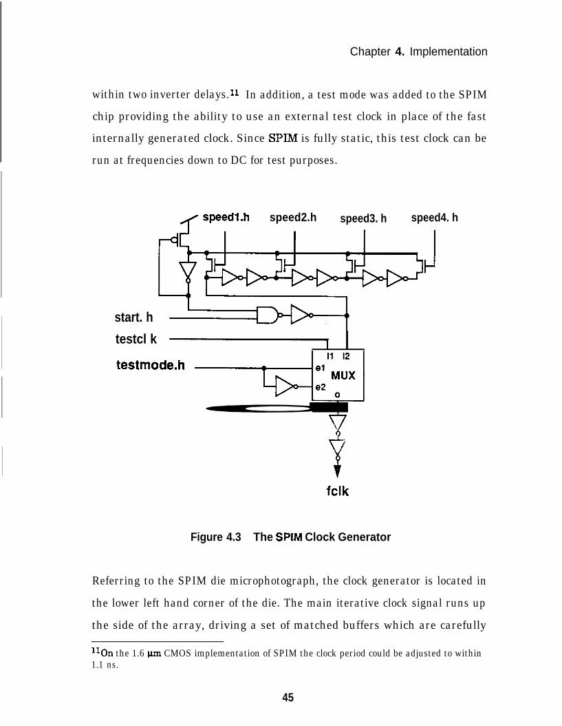
Chapter 4. Implementation
within two inverter delays.11 In addition, a test mode was added to the SPIM
chip providing the ability to use an external test clock in place of the fast
internally generated clock. Since SPIM is fully static, this test clock can be
run at frequencies down to DC for test purposes.
,f speed1.h speed2.h speed3. h speed4. h
start. h
testcl k
testm0de.h
fclk
Figure 4.3 The SPIM Clock Generator
Referring to the SPIM die microphotograph, the clock generator is located in
the lower left hand corner of the die. The main iterative clock signal runs up
the side of the array, driving a set of matched buffers which are carefully
llOn the 1.6 pm CMOS implementation of SPIM the clock period could be adjusted to within1.1 ns.
45
Chapter 4. Implementation
tuned to minimize skew across the array. Wider than minimum metal lines
are used on the master clock line to reduce the resistance of the clock line
relative to the resistance of the driver. The clock and control lines, driven
from the matched buffers, are then run across the entire width of the array in
metal.
When a multiply signal has been received, a small delay occurs while starting
up the clocks. This delay comes from two sources. The first is the logic which
decodes the run signal and starts up the ring oscillator. The second source of
delay arises from the long control and clock lines running across the array.
The 2 pF loads require a buffer chain to drive them. The simulated delay of
the buffer chain and associated logic is 6 ns, almost half a clock cycle. Since
the inputs are latched before the multiply is started, SPIM does the first
Booth encode before the array clocks become active (cycle 0). Thus, the
startup time is not wasted. After the clocks have been started, SPlM requires
seven clock cycles (cycles l-7) to complete the array portion of a multiply.
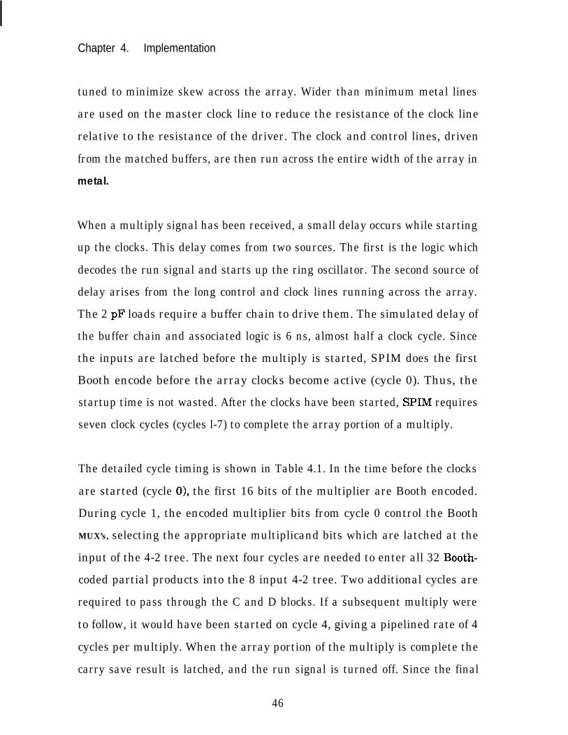
The detailed cycle timing is shown in Table 4.1. In the time before the clocks
are started (cycle 01, the first 16 bits of the multiplier are Booth encoded.
During cycle 1, the encoded multiplier bits from cycle 0 control the Booth
MUX’s, selecting the appropriate multiplicand bits which are latched at the
input of the 4-2 tree. The next four cycles are needed to enter all 32 Booth-
coded partial products into the 8 input 4-2 tree. Two additional cycles are
required to pass through the C and D blocks. If a subsequent multiply were
to follow, it would have been started on cycle 4, giving a pipelined rate of 4
cycles per multiply. When the array portion of the multiply is complete the
carry save result is latched, and the run signal is turned off. Since the final
46
Chapter 4. Implementation
partial sum from the D block is latched into the carry propagate adder only
every fourth cycle, several cycles are available to stop the clock without
corrupting the result.
0 1 2 3 4 5 6 7
Booth Encode
A and B blockBooth MUX’s
A BlockCSA’S
B BlockCSA’S
startupO-15 16-31 32-47 46-63
o-15 1631 32-47 46-63
o-7 1623 32-39 46-55
6-15 24-31 4Q47 56-63
C Block
D Block
o-15 1631 32-47 46-63
clearO-15 1631 32-47 46-63
NOTES: Numbers indicate which partial products are being reduced. 0 is theleast significant bit.
Table 4.1 SPIM Plpe Timing
4.1.3 SPIM Test Results
To accurately measure the internal clock frequency the clock was made
available at an output pin, allowing an oscilloscope to be attached. SPIM was
then placed in continuous (loop) mode where the clock is kept running and
47
Chapter 4. Implementation
multiplies are piped through at a rate of one multiply every 4 cycles. Since
the clock is running continuously its frequency can be accurately determined.
Three components determine the actual performance of SPIM: 1) the start-up
time, when the clocks are started and the first Booth encode takes place (cycle
0); 2) the array time, which includes the time through the Booth select MUX’S,
the 8 input 4-2 tree, and the accumulation cycles (cycles l-7); and 3) the carry
propagate addition time, when the final carry propagate addition converts the
carry-save form of the result from the accumulator to a simple binary
representation. Due to limitations in our test equipment, only the array time
could be accurately measured. Since the array time requires 7 cycles, and the
array clock frequency was 85 MHz, the array time is simply 7*(1/85 MHz) =
82 ns. The startup and carry propagate addition times, based upon
simulations, were 6 and 30 ns respectively. In flowthrough mode, the total
latency is simply the sum of the startup time (6 ns), the array time (82 ns),
and the carry propagate addition time (30 ns), for a total of 118 ns. Thus,
SPIM has a total latency under 120 ns. The throughput of one multiply every
4 cycles, or 40(1/85 MHz) = 47 ns, gives SPIM a maximum pipelined rate in
excess of 20-million multiplies per second.
The performance range of the parts tested was from 85.4 to 88.6 MHz, at a
room temperature of 24.5 ‘C and a supply voltage of 4.9 V. One of the parts
was tested over a temperature range of 5 - 100 ‘C. At 5 ‘C it ran at 93.3
MHz, with speeds of 88.6 and 74.5 MHz at 25 and 100 ‘C, respectively. The
average power consumed at 85 MHz was 72 mA, while only 10 mA was
required in standby mode.
48
Chapter 4. Implementation
4.2 Future ImprovementsWith the implementation of any integrated circuit new things are learned,
and SPIM was no exception. Referring back to the die microphotograph of
SPIM, the A and B blocks are three times as large as the C block. This was
due to the Booth select MUX’S used in the A and B blocks. Each Booth MUX,
with its corresponding latch, is larger than a single CSA. Also, due to the
routing required for the 16-bit shift, the D block is twice as large as the C
block. The array area can be split into four main components: routing, CSA
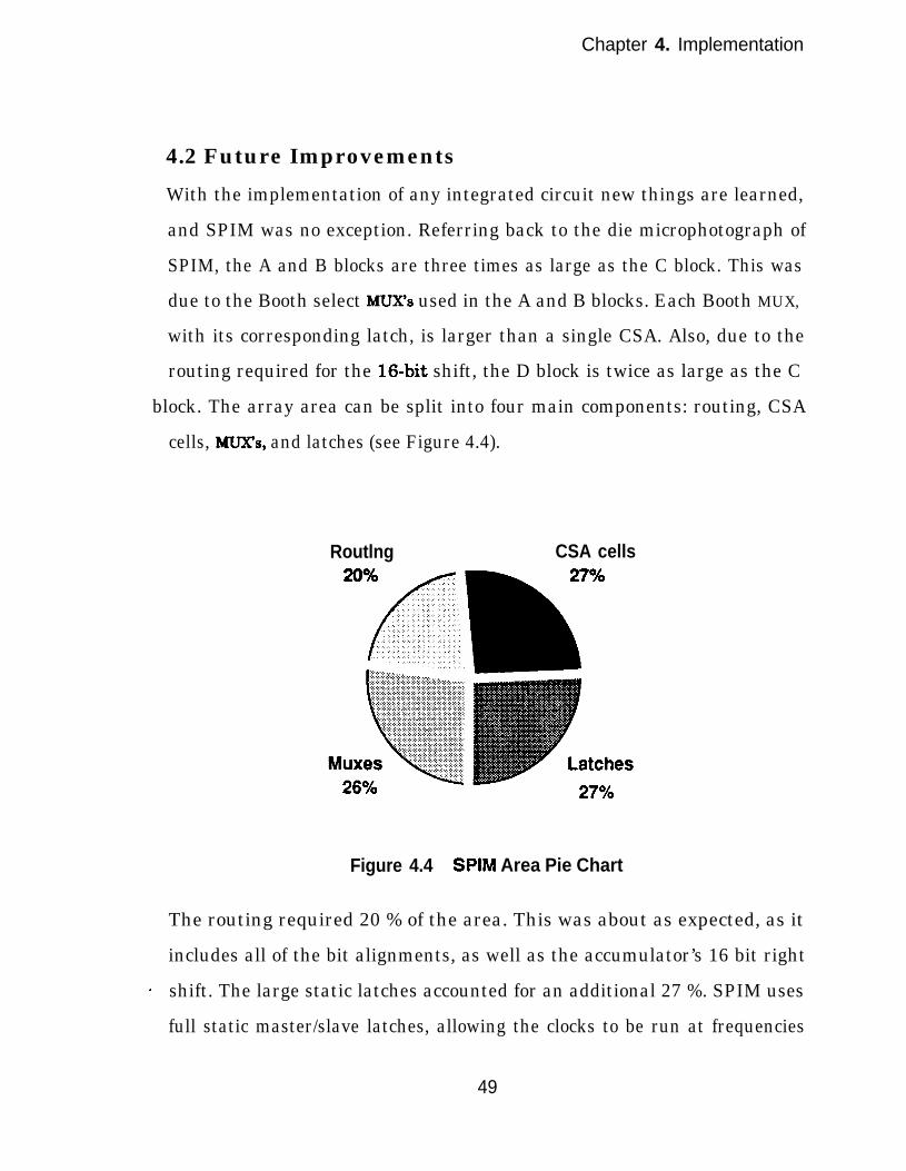
cells, MUXS, and latches (see Figure 4.4).
Routlng CSA cells
Figure 4.4 SPIM Area Pie Chart
The routing required 20 % of the area. This was about as expected, as it
includes all of the bit alignments, as well as the accumulator’s 16 bit right
* shift. The large static latches accounted for an additional 27 %. SPIM uses
full static master/slave latches, allowing the clocks to be run at frequencies
49
Chapter 4. Implementation
down to DC for testing purposes. These latches are quite large. Additionally,
they are slow, requiring 25 % of the cycle time. Since the SPIM architecture
has been proven, smaller, faster, dynamic latches should be used on future
versions.
4-2Adder
G‘CI-8
- Booth : Booth -Booth q Booth q
5= Sel Z Sel I: Sel q- mux - mux - mux - mux -
e 4-25 Adder
mo
4-2Adder
4-2Adder
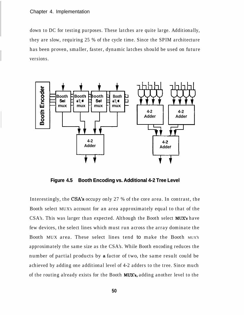
Figure 4.5Figure 4.5 Booth Encoding vs. Additional 4-2 Tree LevelBooth Encoding vs. Additional 4-2 Tree Level
Interestingly, the CM’s occupy only 27 % of the core area. In contrast, the
Booth select MUX’s account for an area approximately equal to that of the
CSA’s. This was larger than expected. Although the Booth select MUX’s have
few devices, the select lines which must run across the array dominate the
Booth MUX area. These select lines tend to make the Booth MUX’S
approximately the same size as the CSA’s. While Booth encoding reduces the
number of partial products by a factor of two, the same result could be
achieved by adding one additional level of 4-2 adders to the tree. Since much
of the routing already exists for the Booth MUX’s, adding another level to the
50
Chapter 4. Implementation
tree requires replacing every two Booth select MUX’s with a 4-2 adder and 4
AND gates (see Figure 4.5). In the case of SPIM, the Booth encoding
hardware can be replaced by an additional tree level without changing the
area of the multiplier core.
The biggest reason for not Booth encoding is that Booth encoding significantly
increases the complexity of the multiplier array. To begin with, Booth
encoding requires additional hardware which must be designed and laid out,
including the encoders and Booth select MUX%. Another problem with Booth
encoding is that it generates negative partial products. An increase in
complexity results in the need to handle these negative partial products
correctly. One example is the sign extension of negative partial products.
Another is the new sticky algorithm, developed in Chapter 6, which only
works on positive partial products. In the case of a floating-point multiplier,
replacing the Booth encoders with an additional level of 4-2 adders would
remove the negative partial products, significantly reducing the multiplier
complexity.
In the case of CMOS 4-2 multipliers, replacing the Booth hardware with an
additional tree level provides a significant reduction in complexity with no
increase in area. On this basis, future CMOS 4-2 multipliers should not use
Booth encoding. Using a larger tree in place of a smaller Booth encoded tree
is a viable alternative on other multiplier trees as well.12 A similar
observation about the size and complexity of Booth encoding was noted in
[JOU 881.
12An exception may be in the case of ECL, where fewer devices may favor the Booth muxesover the C&l’s due to power considerations.
51
Chapter 4. Implementation
Research on pipelined 4-2 trees and accumulators has continued. A test
circuit consisting of a new clock generator and an improved 4-2 adder has
been fabricated in a 0.8 pm CMOS technology. At room temperature the test
chip ran at 400 MHz, demonstrating the potential performance of iterative
4-2 multipliers.
4.3. SummarySPIM was fabricated in a 1.6 pm CMOS process through the DARPA MOSIS
fabrication service. It ran at an internal clock frequency of 85 MHz at room
temperature. The latency for a 64 X 64 bit fractional multiply is under 120
ns. In piped mode SPIM can initiate a multiply every 4 cycles (47 ns), for a
throughput in excess of 20-million multiplies per second. SPIM required an
average of 72 mA at 85 MHz, and only 10 mA in standby mode. SPIM
contains 41,000 transistors with a core size of 3.8 X 6.5 mm, and an array size
of 2.9 x 5.3 mm.
Aside from proving that a small, fast, regular multiplier can be constructed
from this new architecture, one of the more interesting discoveries learned
from the SPIM implementation was that Booth encoding should not be used
in future CMOS 4-2 multipliers. In the case of CMOS, Booth encoding
significantly increases complexity with no performance or area benefits.
While Booth encoding has its place where linear arrays are concerned, these
findings indicate that designers should reconsider the use of Booth encoding
for all future multiplier trees.
52
Chapter 5
Clocking
In previous chapters the architecture and design of multipliers using
pipelined 4-2 trees and accumulators was discussed. To achieve optimal
performance these multipliers must be clocked at a rate equal to the
combinational delay of the 4-2 stages. The correspondingly high clock
frequencies mandate careful attention to clocking. This chapter begins by
addressing the issues involved in generating high-speed clocks. An on-chip
clock generator is proposed which can accurately match, and track, the delay
of the 4-2 multiplier logic. Clock distribution, and use in the 4-2 multiplier
stages, will then be discussed. Finally, performance limits will be evaluated
for present and future technologies.
53

Chapter 5. Clocking
5.1 Clock GenerationThe high speed clocks used in the pipelined 4-2 tree and accumulator must be
matched to the delay of the 4-2 adders for optimal performance. Most system
clocks are typically much slower than required. A special high-speed system
clock could be used; however, system clocks cannot be adequately tuned to the
4-2 adder delay to achieve maximum performance. Another problem is that
the 4-2 logic delay changes with variations in temperature, supply voltage,
and processing. Clocks generated externally to the chip must maintain a
built-in margin of safety to take the worst case scenario of these variations
into account. This safety margin causes a loss in multiplier performance.
Worse yet, failure to keep an adequate margin can cause incorrect results.
These deficiencies with externally generated clocks can be overcome by
generating the multiplier clock on-chip.
5.1.1 A Generic On-Chip Clock Generator
A free running oscillator placed on the chip could be used to generate the
multiplier clock. While it would generate an adequate clock, it does pose
potential synchronization problems between the external system clock and
the internal multiplier clock. Synchronization between any two separate free
running clocks is always a problem. One method to overcome
synchronization problems between two separate clocks is by using a stoppable
clock [CHA 863. A stoppable clock is simply a clock which can be started and
stopped by an external signal. A simple generic stoppable on-chip clock
generation scheme is shown in Figure 5.1. It is implemented using a ring
54

Chapter 5. Clocking
oscillator, and a NAND gate which is placed in the feedback path allowing the
clock to be stopped and started.
Figure 5.1 Generic On-Chip Stoppable Clock Generator
The generic stoppable on-chip clock generator eliminates synchronization
problems. In doing so it also provides a simple system interface. Once the
operands have been loaded, a multiply is initiated. This turns on the run
signal, starting the clock. When the array portion of the multiply is
completed the run signal is turned off, stopping the clock. The fast running
internal multiply clock is not seen by the outside world. To the outside world
the multiplier appears as a simple flow-through part. Like a simple logic
gate, the inputs are applied and sometime later the result is available at the
output pins. As a side benefit, the stoppable clock saves power over a free
running clock. Upon completing a multiply the clock is stopped, which
powers down the entire array.
55
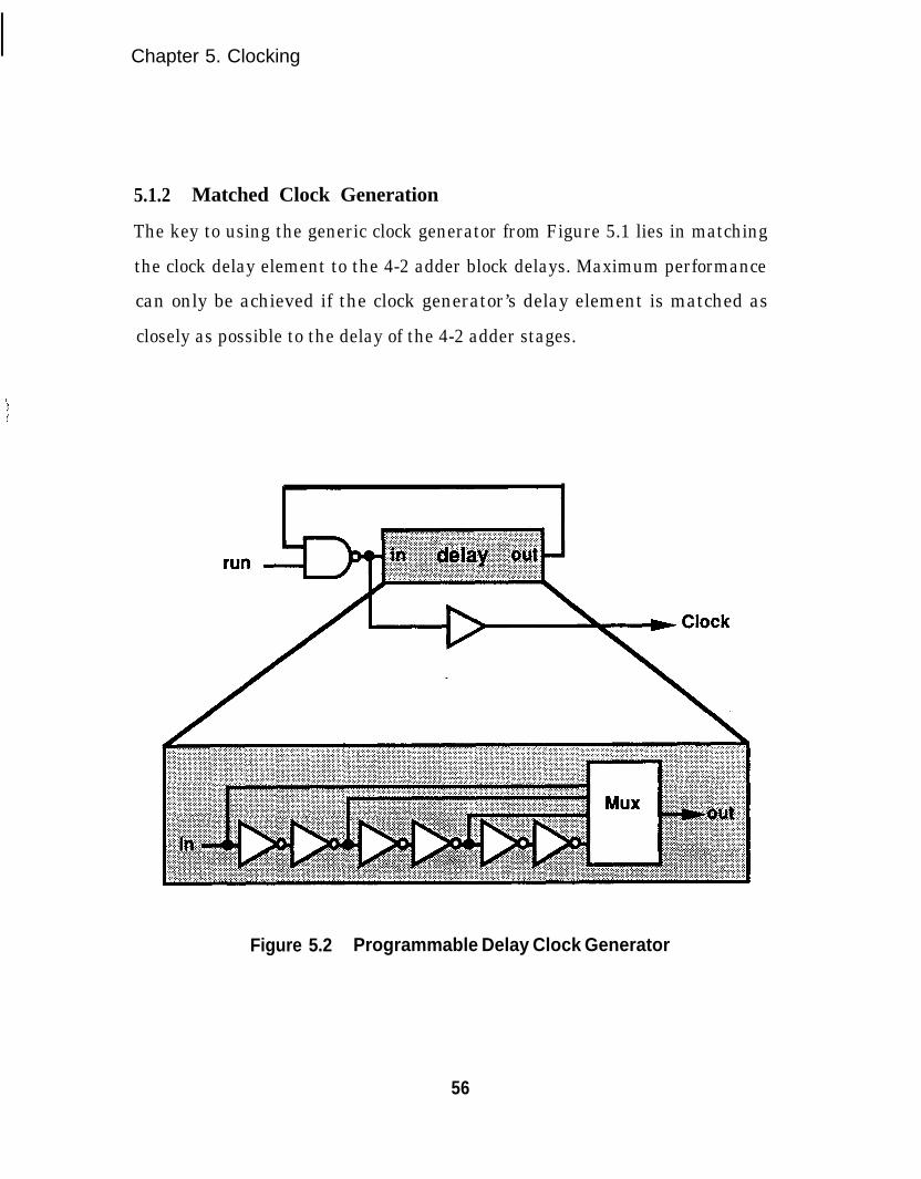
Chapter 5. Clocking
5.1.2 Matched Clock Generation
The key to using the generic clock generator from Figure 5.1 lies in matching
the clock delay element to the 4-2 adder block delays. Maximum performance
can only be achieved if the clock generator’s delay element is matched as
closely as possible to the delay of the 4-2 adder stages.
Figure 5.2 Programmable Delay Clock Generator
56
Chapter 5. Clocking
One technique for matching the clock frequency to the combinational delay of
the 4-2 stage is by using a variable length inverter chain as the delay element
(see Figure 5.2). This technique was used to generate the clocks on SPIM
(refer to Chapter 4). The MUX is used to select the length of the feedback
path. The result is a digitally selectable clock. Maximum performance is
achieved by tuning the clock frequency to match the critical path delay of the
4-2 pipe stage. This is also useful for test purposes. On prototype chips the
clock frequency can be increased until critical patterns fail. This yields both
the critical path and the maximum operating frequency.
As stated, one reason for using an on-chip clock generator is that it can track
the combinational logic delay over process, voltage, and temperature
variations. The variable length inverter chain can be adjusted to compensate
for processing effects. To first order, temperature and supply voltage
variations are also taken into account by the clock generators existence on the
same die as the multiplier. Although existence on the same die is the most
important criterion, other factors such as device size and circuit configuration
can also effect tracking accuracy. The variable length inverter chain
obviously uses different circuitry than the basic 4-2 stage. Second order
effects caused by the different circuit configuration and device sizes can cause
the tracking to be less than optimal. An example of imperfect tracking over
temperature variation can be seen in Figure 5.3.
57
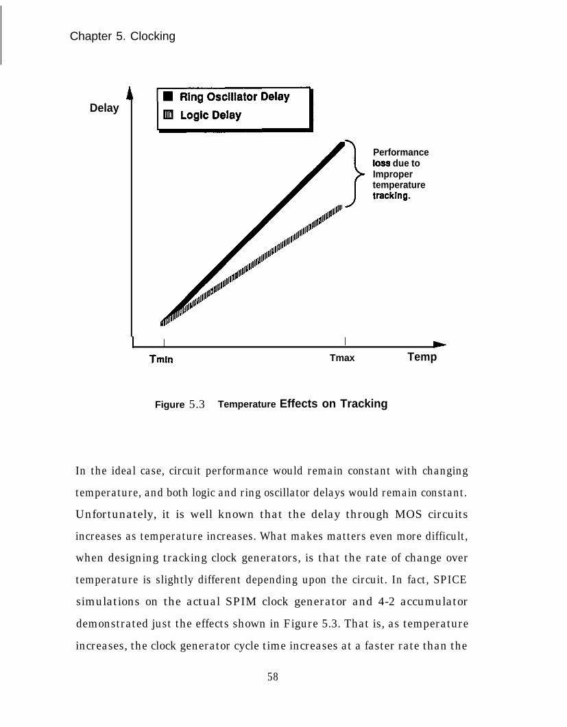
Chapter 5. Clocking
Delay
>
Performanceloss due toImpropertemperaturetracking.
I I I +Tmln Tmax Temp
Figure 5.3 Temperature Effects on Tracking
In the ideal case, circuit performance would remain constant with changing
temperature, and both logic and ring oscillator delays would remain constant.
Unfortunately, it is well known that the delay through MOS circuits
increases as temperature increases. What makes matters even more difficult,
when designing tracking clock generators, is that the rate of change over
temperature is slightly different depending upon the circuit. In fact, SPICE
simulations on the actual SPIM clock generator and 4-2 accumulator
demonstrated just the effects shown in Figure 5.3. That is, as temperature
increases, the clock generator cycle time increases at a faster rate than the
58
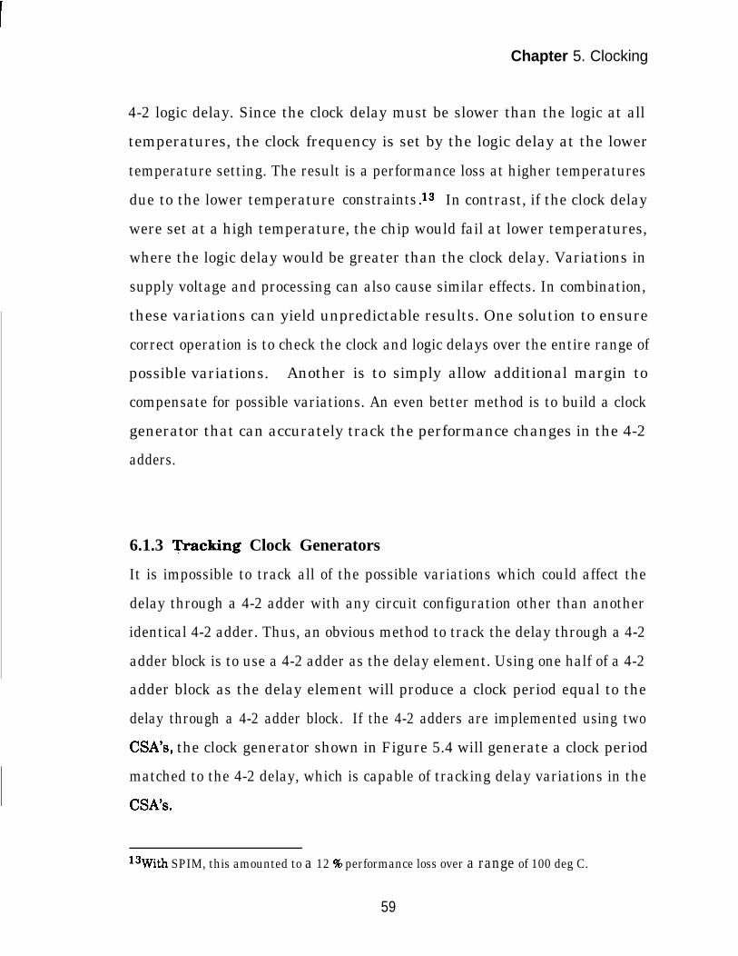
Chapter 5. Clocking
4-2 logic delay. Since the clock delay must be slower than the logic at all
temperatures, the clock frequency is set by the logic delay at the lower
temperature setting. The result is a performance loss at higher temperatures
due to the lower temperature constraints .ls In contrast, if the clock delay
were set at a high temperature, the chip would fail at lower temperatures,
where the logic delay would be greater than the clock delay. Variations in
supply voltage and processing can also cause similar effects. In combination,
these variations can yield unpredictable results. One solution to ensure
correct operation is to check the clock and logic delays over the entire range of
possible variations. Another is to simply allow additional margin to
compensate for possible variations. An even better method is to build a clock
generator that can accurately track the performance changes in the 4-2
adders.
6.1.3 Tf’racking Clock Generators
It is impossible to track all of the possible variations which could affect the
delay through a 4-2 adder with any circuit configuration other than another
identical 4-2 adder. Thus, an obvious method to track the delay through a 4-2
adder block is to use a 4-2 adder as the delay element. Using one half of a 4-2
adder block as the delay element will produce a clock period equal to the
delay through a 4-2 adder block. If the 4-2 adders are implemented using two
CM’s, the clock generator shown in Figure 5.4 will generate a clock period
matched to the 4-2 delay, which is capable of tracking delay variations in the
CSA’s.
13With SPIM, this amounted to a 12 % performance loss over a range of 100 deg C.
59
Chapter 5. Clocking
run.h
A B Cin
CSA
- Clk
Figure 5.4 A CSA Tracking Clock Generator14
One obvious problem with the clock generator in Figure 5.4 is that it is
difficult to use with direct 4-2 adder implementations where a convenient
place to split the 4-2 adder may not exist. It also overlooks the fact that the
critical path will contain more than a single 4-2 adder and its half latches. In
practice, the 4-2 accumulator is the slowest pipe stage in the multiplier.
Additional loading caused by the wiring needed for the right shift, and
hardware required to zero the accumulator, decreases the accumulator’s
performance compared to a basic 4-2 adder. The full delay of the 4-2
accumulator can be taken into account by using the entire accumulator,
including the wiring loads and additional logic, as a delay element (see Figure
5.5).
l?lYhe clock generator shown in Figure 5.4 was fabricated in a 0.8 pm CMOS technology. Itgenerated a 400 MHz clock which was used to clock a dual CSA 4-2 adder. The clockgenerator worked well, and was definitely a step in the right direction.
60

Chapter 5. Clocking
run
4-2
latch
I
4! “k
Figure 5.5 A 4-2 Tracking Clock Generator
Using the 4-2 accumulator for the delay element produces a matched delay
which will track the actual 4-2 accumulator, but the corresponding period is
twice as long as desired. An XOR gate can be used to produce a pulse each
cycle. Setting the pulse width to a 50 % duty cycle in effect doubles the clock
frequency, producing the desired result. A duty cycle near 50 % is desirable
because narrow pulses can shrink, or even be lost, when passing through long
buffer chains.15
Non-symmetrical edges caused by the difference in P and N-channel devices
also cause a “data dependency” in combinational logic. That is, once the
15SPICE simulations of CMOS buffer chains have shown that the minimum pulse width thatcan be successfully passed through a buffer chain without significant narrowing is on theorder of three inverter delays. Mismatches between P and N-channel devices may require aneven wider pulse due to the difference in the rising and falling edges.
61

Chapter 5. Clocking
critical path has been determined, the delay through that path will be
different depending upon the input. 16 This data dependency can cause a
failure in the clock generator. The P and N devices could be matched to
adjust rise and fall times and balance the delay but, with changing
technologies, and even from one fabrication to the next, the device
mismatching will tend to vary. Another solution to the data dependency
problem can be seen in Figure 5.6.
runI
4-2 4-2I
Figure 5.6 A Dual 4-2 Tracking Clock Generator
l%PICE simulations of CM’s have shown that this difference can be as large as 20 96 ormore.
62
Chapter 5. Clocking
The dual 4-2 tracking clock generator uses two 4-2 blocks as delay elements.
An input is placed into the critical path of one of the 4-2 blocks with the
complemented input placed into the other. Data dependencies will cause the
outputs to arrive at different times. The circuit at the bottom of the two 4-2
blocks is a non-overlapping latch.17 This structure t&states until both of the
4-2 outputs are different before passing a signal. The effect is that the delay
is always as long as the slower path. This eliminates data dependent race
conditions from the clock generator. ’
5.1.4 Implementing Tracking Clock Generators
To implement a dual 4-2 tracking clock generator the critical path through
the 4-2 accumulator must first be found. This can be accomplished by SPICE
simulation. The critical path must then be examined for any logic hazards.
Spikes could potentially propagate to the clock line with disastrous results.
Typically, the critical path is dependent upon only one input changing. This
makes logic hazards less likely, and simpler to detect and correct.
Another potential problem is that of a slow moving node. The problem occurs
when a slow node, which is part of the clock generator, does not fully rise or
fall faster than the oscillation period. This is actually another case where the
delay is data dependent. In the pipelined tree the same data value may be
applied to a node over several cycles. As a result, several cycles may be
available for the node to reach its final supply rail voltage. In contrast, all of
1 ‘The non-overlapping latch structure is one possible implementation of what is also knownas a Muller C element in asynchronous designs.
63
Chapter 5. Clocking
the oscillating nodes in the clock generator must undergo a transition from
one logic level to the other on each clock cycle. If the oscillating node does not
completely reach its supply rail in a given cycle, on the next cycle the node
will not have to move as far to reach the opposite supply rail. A smaller
voltage swing takes less time. This decreases the delay, resulting in a clock
which oscillates too fast. SPICE simulations should be used to detect any
potentially slow nodes.
Using a 4-2 accumulator as the delay element provides excellent tracking;
however, the required delay is slightly longer than that produced by the
accumulator alone. One reason is that the 4-2 element used as the delay
element has its latch elements tied fully on. This does not allow for the edge
rates of the actual clock lines .ls The result is that the delay through the
latches in the clock generator is less than the latch delay in 4-2 accumulator
at the base of the 4-2 tree.
Skew is another factor not taken into account by the dual 4-2 matched clock
generator. Fortunately, the skew across the 4-2 tree is not a major problem.
The reason is that each 4-2 adder slice only communicates with the adjacent
slice. Clock skew only matters between latched 4-2 adders which
communicate with each other. In the partial, pipelined 4-2 multiplier and
accumulator, the widest number of bits across which 4-2 adders talk to each
other are K bits of the accumulator for a partial tree size of K bits. To
determine the skew across these K bits of the accumulator there are two
possible sources. The first is at the beginning of the array due to a mismatch
l*Long clock lines are lossy transmission lines. Resistance in the wires causes the edges tobecome less sharp as the distance from the source increases.
64

Chapter 5. Clocking
in the clock buffers. As each row of 4-2 adders in the layout is exactly the
same, the load on the clock lines across each row in the array is identical. By
using matched buffers to drive the identically loaded clock lines across the
array, the skew between vertical rows will be small (refer to section 5.4). The
other possible source of skew is due to a mismatch in the clock wave-front
propagation time across the K bits. Since the loads across the array are
balanced this skew should also be negligible. Assuming the loads and buffers
are balanced, the sum of the clock skews across K bits of the accumulator
should only be on the order of a few tenths of a gate delay.
When implementing the clock generator, it turns out that if the clock buffers
are sticiently sized and matched so that the clock edges are sharp and the
skew is small, the added delay of the series NAND gate, inverter, and non-
overlapping latch used in the clock generator will typically be sufficient to
compensate for the added latch delay and skew. If the clock generator is still
slightly too fast, there are two simple ways to slow it down. The first is to
provide some additional load capacitance which can be added to the feedback
path. Care should be taken to ensure that the feedback node does not become
slower than the clock frequency. An alternative is to increase the length of
the feedback path by adding a variable length delay element in series with
the 4-2 adder delay (refer to Figure 5.2). One last useful addition to the clock
generator is a test clock input, as was provided on the SPIM chip (see chapter
4: Implementation). This allows the rest of the chip to be tested in the event
of a complete clock failure. A dual 4-2 matched clock generator with a slow
down capacitor and test clock input is shown in Figure 5.7.
65
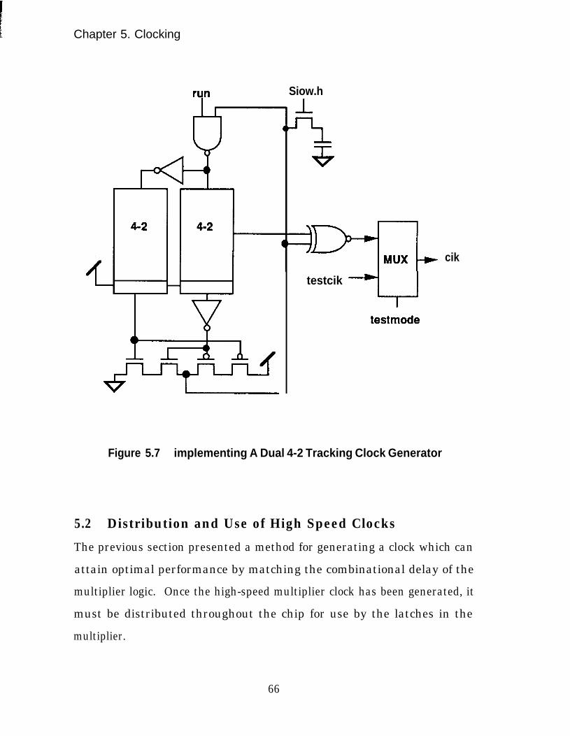
Chapter 5. Clocking
run Siow.h
testcik
--utestmode
cik
Figure 5.7 implementing A Dual 4-2 Tracking Clock Generator
5.2 Distribution and Use of High Speed ClocksThe previous section presented a method for generating a clock which can
attain optimal performance by matching the combinational delay of the
multiplier logic. Once the high-speed multiplier clock has been generated, it
must be distributed throughout the chip for use by the latches in the
multiplier.
66
Chapter 5. Clocking
6.2.1 Clock Waveforms
One obvious method for clocking 4-2 adders is to use the two-phase non-
overlapping clock methodology made popular by Carver Mead and Lynn
Conway [MEA 801. The problem with two-phase non-overlapping clocks at
high frequencies is that they have four separate timing events which must be
controlled; phase 1 rising, phase 1 falling, phase 2 rising, and phase 2 falling
[NOI 831. Maintaining tight control over these separate events at high
frequencies becomes difficult. Each pair of timing events requires a separate
and distinct pulse. Thus, two-phase non-overlapping clocks require two
separate and distinct pulses per clock period. A single clock has only two
timing events; clock rising and clock falling. As such, a single clock requires
only one distinct pulse per clock period. This means that, given the same
pulse width restrictions and skew problems, a single clock can safely operate
at higher frequencies than a two-phase non-overlapping clock. Wiring
overhead and skew problems are also reduced by globally distributing a
single clock, as opposed to two distinct clocks. The performance and
distribution advantages make a single clock better suited for global high
frequency clocking than two-phase non-overlapping clocks.
5.2.2 Clock Distribution
In generating the clocks it was noted that edge rates affect performance.
Slow clock edges slow down the latches. Another important consideration
when distributing clocks is skew. Both the clock rise times and skew can be
minimized by proper clock distribution.
67
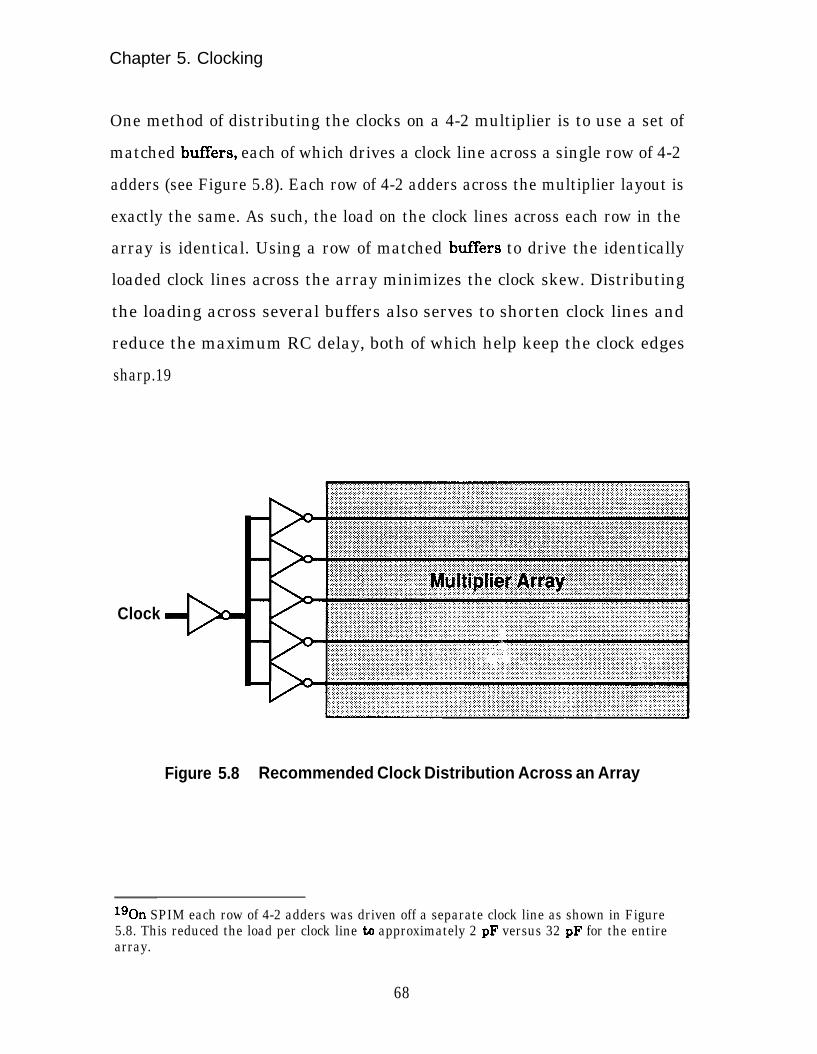
Chapter 5. Clocking
One method of distributing the clocks on a 4-2 multiplier is to use a set of
matched buffers, each of which drives a clock line across a single row of 4-2
adders (see Figure 5.8). Each row of 4-2 adders across the multiplier layout is
exactly the same. As such, the load on the clock lines across each row in the
array is identical. Using a row of matched buffers to drive the identically
loaded clock lines across the array minimizes the clock skew. Distributing
the loading across several buffers also serves to shorten clock lines and
reduce the maximum RC delay, both of which help keep the clock edges
sharp.19
Clock
Figure 5.8 Recommended Clock Distribution Across an Array
lgOn SPIM each row of 4-2 adders was driven off a separate clock line as shown in Figure5.8. This reduced the load per clock line to approximately 2 pF versus 32 pF for the entirearray.
68
Chapter 5. Clocking
6.2.3 Latching 4-2 Adder Stages
Once the single 4-2 multiplier clock has been generated and distributed to the
array, it must be used to clock the latch structures in the 4-2 adder stages.
Single-phase clocking is typically not used in general VLSI systems because it
requires satisfying two-sided timing constraints. In other words, there must
be both a maximum, and a minimum restriction on the clock pulse width. In
contrast, two-phase clocking schemes require that only single sided
constraints be satisfied, restricting only the minimum pulse width. The two-
sided constraints create enough added complexity that the additional
hardware required to yield single-sided constraints, as in strict two-phase, is
often a worthwhile trade-off for large complex general systems where slower
clocks are used. As explained in the previous section, the problem with two-
phase clocks is that global distribution and control of high frequency multiple
phase clocks is difficult. This makes the use of a single global clock
preferable; however, to be successful the two-sided constraints must either be
eliminated, or dealt with using balanced pipe stages.
Several pseudo single-phase clocking schemes, potentially suitable for general
systems, have been developed which remove the two sided timing constraints
by using two different types of latches [GON 83]lJ!ICG 87]ryUA 891. The two
types of latches, typically N and P, are clocked by the high and low phase of
the same clock respectively. Normally these latches are more complex than a
simple dynamic half latch. Also, degraded logic levels are typically found in
these latch structures. The added complexity and degraded levels tend to
make these latches bigger, slower, and less safe than simple dynamic half
latches.
69
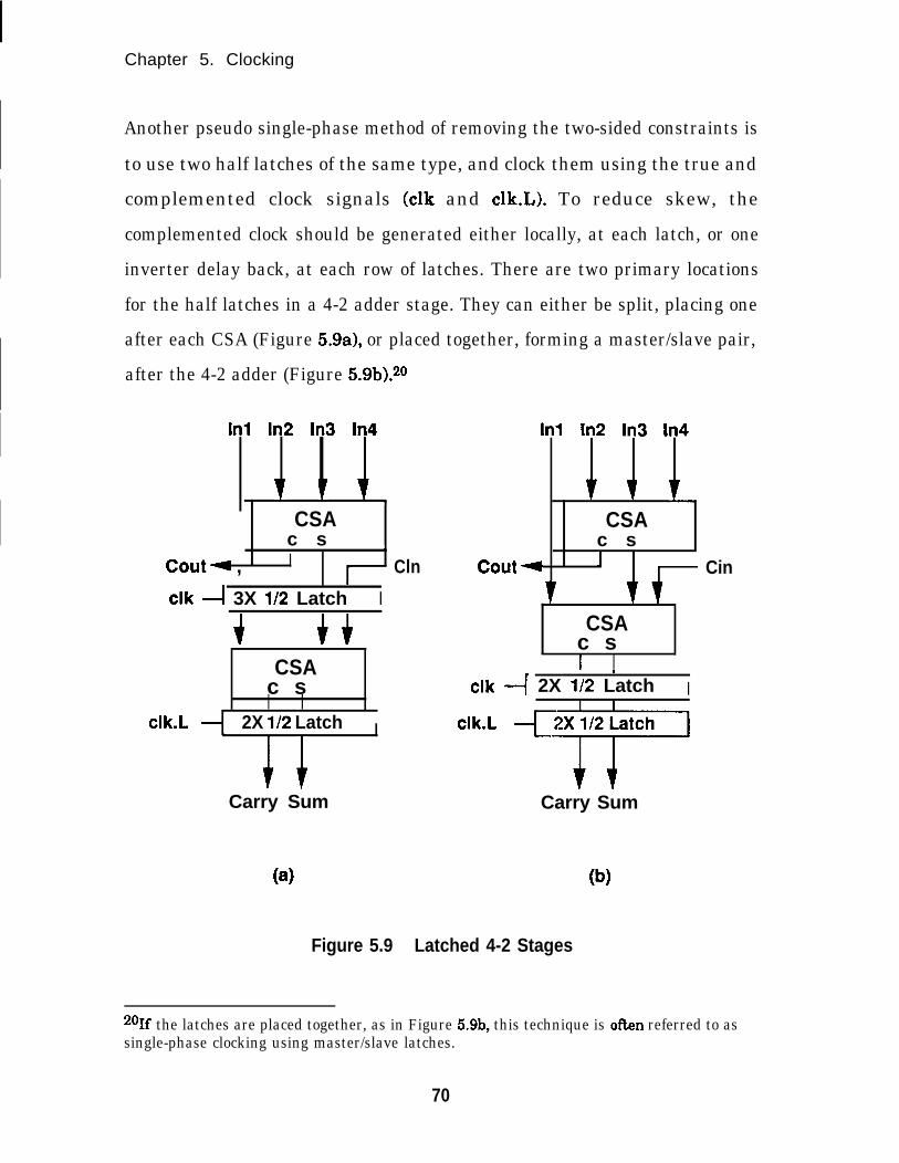
Chapter 5. Clocking
Another pseudo single-phase method of removing the two-sided constraints is
to use two half latches of the same type, and clock them using the true and
complemented clock signals (elk and c1k.L). To reduce skew, the
complemented clock should be generated either locally, at each latch, or one
inverter delay back, at each row of latches. There are two primary locations
for the half latches in a 4-2 adder stage. They can either be split, placing one
after each CSA (Figure 5.9a), or placed together, forming a master/slave pair,
after the 4-2 adder (Figure 5.9bj.20
In1 In2 In3 In4
1 f +CSA
c s 4tout- , I
1 Cln
elk 4 3X l/2 Latch I
Cout
CSAc sI I
c1k.L 2X l/2 Latch I
Carry Sum
00
In1 In2 In3 In4
1 1.CSA
c s* 1
fCSA
c sI I
I
elk 4 2X l/2 Latch I
clk.L +T
T tCarry Sum
W
Figure 5.9 Latched 4-2 Stages
Cin
201f the latches are placed together, as in Figure 5.9b, this technique is often referred to assingle-phase clocking using master/slave latches.
70
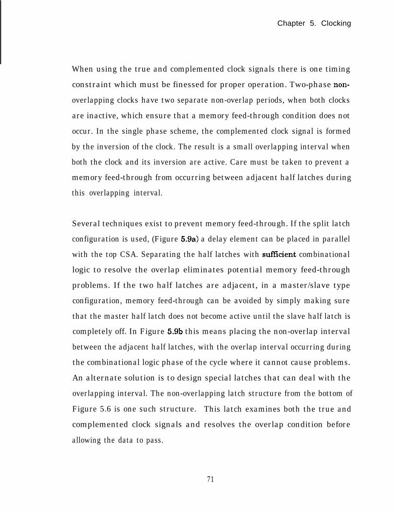
Chapter 5. Clocking
When using the true and complemented clock signals there is one timing
constraint which must be finessed for proper operation. Two-phase non-
overlapping clocks have two separate non-overlap periods, when both clocks
are inactive, which ensure that a memory feed-through condition does not
occur. In the single phase scheme, the complemented clock signal is formed
by the inversion of the clock. The result is a small overlapping interval when
both the clock and its inversion are active. Care must be taken to prevent a
memory feed-through from occurring between adjacent half latches during
this overlapping interval.
Several techniques exist to prevent memory feed-through. If the split latch
configuration is used, (Figure 5.9a) a delay element can be placed in parallel
with the top CSA. Separating the half latches with sufEcient combinational
logic to resolve the overlap eliminates potential memory feed-through
problems. If the two half latches are adjacent, in a master/slave type
configuration, memory feed-through can be avoided by simply making sure
that the master half latch does not become active until the slave half latch is
completely off. In Figure 5.9b this means placing the non-overlap interval
between the adjacent half latches, with the overlap interval occurring during
the combinational logic phase of the cycle where it cannot cause problems.
An alternate solution is to design special latches that can deal with the
overlapping interval. The non-overlapping latch structure from the bottom of
Figure 5.6 is one such structure. This latch examines both the true and
complemented clock signals and resolves the overlap condition before
allowing the data to pass.
71
Chapter 5. Clocking
An alternative to using two half latches is to use a single half latch clocked off
a single multiplier clock (see Figure 5.10). This is a true single-phase clocked
structure, using only a single clock line. No additional clocks or inverted
clock signals are used. In true single-phase clocking, the high period of the
clock acts as a “pulse” which activates the latches.21 This pulse has a two
sided timing constraint. It must be wide enough to allow the data to flow
through the latch. This is the minimum pulse width. The maximum pulse
width must be less than the time through the half latch plus the shortest
time through any logic block between two half latches. The clock period will
be the time through a half latch plus the longest path through a logic block.
In1 In2 In3 In4
Cout 1 4-2 Adder + Cin
elk 4 2X l/2 Latch 1
Carry Sum
Figure 5.10 Single Half Latched 4-2 Adder
21To distinguish true single-phase clocking from the pseudo single-phase clocking schemes, itwill be referred to as “pulsed single-phase clocking”.
72

Chapter 5. Clocking
Problems occur with pulsed single-phase clocking schemes when very short
paths exist through the logic block. At the limiting case, if no logic were
between two level-sensitive half latches, the maximum and minimum pulse
widths would be the same. Under these conditions the structure would not
work. Either the latches would not have time to work, or a condition known
as memory feed-through would occur. Ideally, the logic should be balanced so
that all of the paths have equal delays between latches. Balanced paths
provide the widest margin between the maximum and minimum pulse
widths. This is important since very narrow pulses may suffer pulse
narrowing when passing through a buffer chain. An advantage of a 4-2
pipelined multiplier over more general structures is that most of the pipe
stages are, in fact, very similar. They are also all on the same chip. This
makes balancing the pipe stages and maintaining this balance over
temperature, voltage, and process variations more practical.
Various tradeoffs and design considerations exist when choosing either of the
two half latch or single half latch approaches. The pulsed single-phase
clocking is slightly more risky, but it reduces the latch overhead by a factor of
two. Measurements on existing CMOS structures show that the savings in
4-2 area range from 5 to 20 % over using two half latches, with the
performance increases in the 10 to 15 % range. Assuming small, fast latches
are used, the small gains in area obtained by using a single half latch could
be offset by any additional hardware required to balance the pipe stages.
Wires take up lots of space in CMOS chips. Using n-channel only pass
devices, as opposed to full transmission gates, reduces the number of clock
lines running across the array by a factor of two. Although a small loss in
73

Chapter 5. Clocking
noise margin occurs, using n-channel only pass devices reduced the 4-2 area
by 7 to 14 96 on the measured structures with no loss in performance.
Another big win is in using dynamic latches over static latches. Since all of
the 4-2 adders in the array are clocked on every cycle, dynamic latches are
kept refreshed so that static latches are not required. In the CMOS latch
structures that were studied, dynamic latches yielded 10 to 20 % area savings
over static latches.
5.2.4 Conclusions
At very high frequencies a single global clock should be used over multiple
phase clocks. The additional pulses which must be generated and maintained
limit multiple phase clocks at high frequencies. The single-phase clock
should be symmetric, 50 8 duty cycle, to reduce pulse narrowing through
buffer chains. The global clock should be distributed across the array to limit
RC effects so clock edges remain sharp, reducing latch slow down caused by
clock edges.
Any of the three latch structures presented, split, master/slave, or pulsed,
appear to be acceptable choices for latching 4-2 adders. All three should be
considered based upon technology and latch design. While the single latch is
half the size and twice the performance of comparable double latches, two
side timing constraints make it slightly more risky than the other methods.
Larger slower latches favor the single half latch, while faster smaller latches
tip the scales toward the safer dual latch configurations.
74
Chapter 5. Clocking
5.3 Performance Limits
With any integrated circuit, one of the most often ask questions is, ‘how fast
will it go?” In the case of 4-2 multiplier trees and accumulators, performance
is determined by the cycle time and the size of the partial tree. The partial
tree size will be set based upon area constraints. Once the partial tree size is
chosen, the performance is then limited by the cycle time. Using the 4-2
accumulator as the delay element in the clock generator sets the clock
frequency. Thus, for any new technology, once the partial tree size has been
chosen, determining the 4-2 accumulator delay will yield the multiplier
performance. This is the case as long as the clock frequency is actually
limited by the 4-2 delays and not by other factors. The following section will
demonstrate that the 4-2 accumulator delay does, in fact, limit the clock
frequency. It will then be shown that, as technologies shrink, this will
continue to be the case for some time.
5.3.1 Factors Limiting Performance
To determine if the 4-2 delay does indeed limit performance, other
potentially limiting factors must be considered. In the 4-2 multiplier core the
accumulator block has been identified as the slowest logic block. The
additional wiring and zero logic make it slower than any of the 4-2 stages in
the tree. Although care must be taken when designing the control and
pipelined rounding logic, all of the peripheral multiplier logic is relatively
simple and can be designed to run faster than the accumulator. As
technologies shrink all combinational logic will speed up at approximately the
same rate, so the accumulator should continue to be the slowest logic block.
75
Chapter 5. Clocking
On the other hand, wire performance does not increase at the same rate as
the combinational logic. For this reason, a key place to look for performance
limits as technologies shrink is at the long wires in a system.‘
The two sources of long wires in the multiplier are the clock lines and the
data inputs, both of which must drive across the entire multiplier array.22
The multiplier input data lines are the same length, and have approximately
the same loading, as the clock lines. There are, however, two basic
differences between the data and clock lines. In the case of the data lines, the
buffering required to drive these wires must occur during the same cycle as
the logic transition. This is not the case with the clock lines, where the buffer
time is not part of the cycle time. On the other hand, the clock lines must
undergo two rail to rail voltage transitions in each clock cycle, while the data
lines undergo, at most, one transition. In slower technologies, say 2 pm
CMOS, the buffer time will cause the data lines to limit the maximum clock
frequency before the clock lines. This is not an issue, however, as the 4-2
accumulator is the limiting factor in slower technologies. With shrinking
technologies, buffers will become faster relative t.9 wires. As a result, clock
lines will most likely limit system performance before data lines.
5.3.2 Clock Line Limits
When determining the limits on how fast a clock line can be driven in a given
technology, several constraints should be considered. These include:
22Control lines which must run across the array (i.e. the signal which zeros the accumulator)are basically the same as data lines for the sake of this discussion.
76
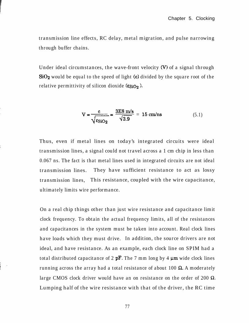
Chapter 5. Clocking
transmission line effects, RC delay, metal migration, and pulse narrowing
through buffer chains.
Under ideal circumstances, the wave-front velocity (v) of a signal through
SiO2 would be equal to the speed of light (c) divided by the square root of therelative permittivity of silicon dioxide (sSi02 >.
VZ~&= 3EJ.-$s = 15cmIns (5.1)
Thus, even if metal lines on today’s integrated circuits were ideal
transmission lines, a signal could not travel across a 1 cm chip in less than
0.067 ns. The fact is that metal lines used in integrated circuits are not ideal
transmission lines. They have sufficient resistance to act as lossy
transmission lines, This resistance, coupled with the wire capacitance,
ultimately limits wire performance.
On a real chip things other than just wire resistance and capacitance limit
clock frequency. To obtain the actual frequency limits, all of the resistances
and capacitances in the system must be taken into account. Real clock lines
have loads which they must drive. In addition, the source drivers are not
ideal, and have resistance. As an example, each clock line on SPIM had a
total distributed capacitance of 2 pF. The 7 mm long by 4 pm wide clock lines
running across the array had a total resistance of about 100 Q. A moderately
large CMOS clock driver would have an on resistance on the order of 200 Sz.
Lumping half of the wire resistance with that of the driver, the RC time
77
Chapter 5. Clocking
constant would be about 500 ps. Assuming a near rail to rail sinusoidal clock
waveform, this would limit the maximum clock frequency to about 500 MHz.
To improve performance, the clock buffer size and wire width could both be
increased, but practical considerations would most likely limit the maximum
clock frequency for a 64 bit wide array in a 2 p CMOS process to around 1
GHz.
Another point of concern with high-speed clocks is that of pulse narrowing
through long buffer chains. High frequency pulses passed through buffer
chains can be narrowed or even disappear. SPICE simulations have shown
that the shortest clock period which can be passed through a buffer chain
without pulse narrowing is on the order of 3 inverter delays. This limits the
clock frequency to about 300 MHz in a 2 pm process. Since buffer chain
performance increases at the same rate as the combinational logic it should
not become a factor as technologies shrink.
Metal migration is a problem associated with high; current densities. While
this would appear to be a major problem for high-speed clocks, recent studies
have shown that metal migration is much less of a problem for AC current, as
found on clock lines, than it is for DC current found on power lines [LIE 891.
Based on these studies, metal migration should not be a significant problem
for high-speed clocking.
SPICE simulations on various 4-2 accumulators in a 2 pm CMOS process
have shown that it is difficult to exceed frequencies on the order of 100 MHz.
Compared to limits of 1 GHz, and 300 MHz imposed by RC delays and buffer
78

Chapter 5. Clocking
narrowing limits respectively, the 4-2 accumulator block clearly limits the
maximum operating clock frequency for 2 pm CMOS technologies.
5.3.3 Effects of Scaling on Performance
Given the same metal layer, as technology shrinks the sheet resistance of the
metal clock lines should remain relatively constant, since the length and
width will both shrink linearly. In practice, many fabrication facilities are
changing from aluminum to tungsten wires in an attempt to reduce metal
migration in their sub-micron technologies. Tungsten wires have roughly
twice the sheet resistance of aluminum wires. Thus, switching to tungsten
wires, when shrinking the technology, tends to double the sheet resistance of
the clock lines. Wires also tend to become thinner in more advanced
technologies, further increasing the clock line resistance.
Capacitance is a function of area and dielectric thickness. If the oxide
thickness remained constant, the capacitan-e would decrease as the square of
the linear shrink. In practice, the oxide thickness has decreased with
shrinking technologies. This acts to increase capacitance. As technologies
shrink, coupling and fringing capacitances make up a larger portion of the
wire capacitance, and even tend to dominate in more advanced technologies.
Over past technology shrinks these effects have caused the capacitance to
decrease at a near linear rate, rather than as the square of the linear shrink.
Given higher sheet resistances and decreased oxide thickness, a 1 cm long
wire in a more aggressive technology will be slower than a 1 cm long wire in
an older technology. Counteracting this effect is the fact that a fixed bit
79
Chapter 5. Clocking
width multiplier will have shorter clock lines in the new technology. The
combined resistance and capacitance effects on the clock lines, including
fringing and coupling, mean that upon shrinking technology wires running
across a fixed bit width multiplier array will undergo an improvement in
performance which is somewhat less than linear. In contrast, recent
technology shrinks have yielded performance increases slightly better than
linear for combinational logic. The bottom line is that when shrinking a fixed
width multiplier, the combinational logic performance will increase at a
faster rate than the wire performance. If this trend continues the wires will
eventually limit performance. This limit is not likely to arise for a while,
however. A test circuit fabricated in a 0.8 p CMOS process ran at 400 MHz.
This was still well below the maximum clock frequency for a 64 bit multiplier
in that technology. Based on current trends, as future CMOS technologies
drop well below the 0.5 p range it should be possible to construct double
precision iterative 4-2 multipliers with clock frequencies approaching 1 GHz.
5.4 Summary
An on-chip clock generator can provide better performance than off chip
clocks by more closely matching the combinational delay through the 4-2
stages. A stoppable clock generator was presented which provides a simple
system interface that is free from synchronization failure. By using the
existing accumulator block as the delay element, the clock generator can
track changes in accumulator performance over variations in temperature,
supply voltage, and processing. A dual accumulator design can even account
for data dependent delays through the 4-2 accumulator. By accurately
80
Chapter 5. Clocking
matching and tracking the critical path delay in the multiplier, the final dual
4-2 accumulator clock generator design can provide near optimal performance
with a high degree of safety.
In looking at global high-speed clock distribution it was determined that
single-phase clocks are preferable to multi-phase clocks. Single-phase clocks
require control over only one timing pulse, compared to two or more in the
case of multi-phase clocks. Single-phase clocks also reduce skew and wiring
overhead compared to multi-phase clocks. To utilize the high-speed single-
phase clocks, several possible latch configurations were proposed. Since
many latches are used in 4-2 pipelined multipliers, the latch overhead can be
high in terms of area and performance. For this reason, each of the several
different latch configurations proposed should be evaluated for future
designs. Although there was no clear winner among the CMOS latch
structures studied, either of the dual half latch configurations seem to be a
good choice if small, fast, dynamic latches are used. As for latch
implementation, dynamic n-pass latchc s appear to be a good choice for
iterative 4-2 multiplier designs in CMOS.
Currently clock performance is limited by the combinational delay of the 4-2
accumulator. As technologies shrink wires become slower relative to devices.
Eventually, driving the clock lines may become the limiting factor. Given the
current constraints and assumptions this should not be the case until CMOS
technologies drop well below the 0.5 p range, with multipliers operating at
frequencies approaching 1 GHz.
81

Chapter 6
IEEE Rounding
Many applications exist in which integer, or non IEEE floating-point,
multiplication is suf%ient. However, to be widely accepted, current and
future floating-point coprocessors must adhere to IEEE standard 754 for
binary floating-point arithmetic [IEE 851. The standard can be implemented
in software, hardware, or a combination of the two [COO 801. The
performance requirements of modern digital systems demand direct
hardware floating-point multipliers. To match the performance of the
hardware multipliers, the rounding modes must also be implemented in
hardware.
Three algorithms will be presented for implementing round to nearest/up. It
will then be shown how the round to nearest/up result can be adjusted to
produce the correct IEEE rounded result. In addition, three methods will be
83
Chapter 6. IEEE Rounding
presented for computing the sticky bit. All of the rounding algorithms and
sticky methods presented are technology independent and can be used with
several types of multiplier architectures. Finally, the additional hardware
required to implement IEEE rounding on iterative 4-2 multipliers will be
studied. It will be shown that iterative 4-2 multipliers require less additional
rounding hardware than full trees, with no performance penalty.
6.1 IEEE Floating-Point FormatsIEEE floating-point numbers are composed of three fields: the sign (s), a
biased exponent (e), and a fraction (0. IEEE floating-point numbers are of
the form:
(-1)‘2E(bo.blb2...bn)
where: s = the sign bit (0, or 1)
E = The exponent
f = The n bit fraction = blb...bn
bo = 1 (bo is an implied 1)
There are four formats defined in the standard. These are single, single
extended, double, and double extended. The bit ordering for all of the formats
is the same, only the length of the exponent and fraction fields varies. Figure
6.1 is an example of the double precision floating-point format. The double
84
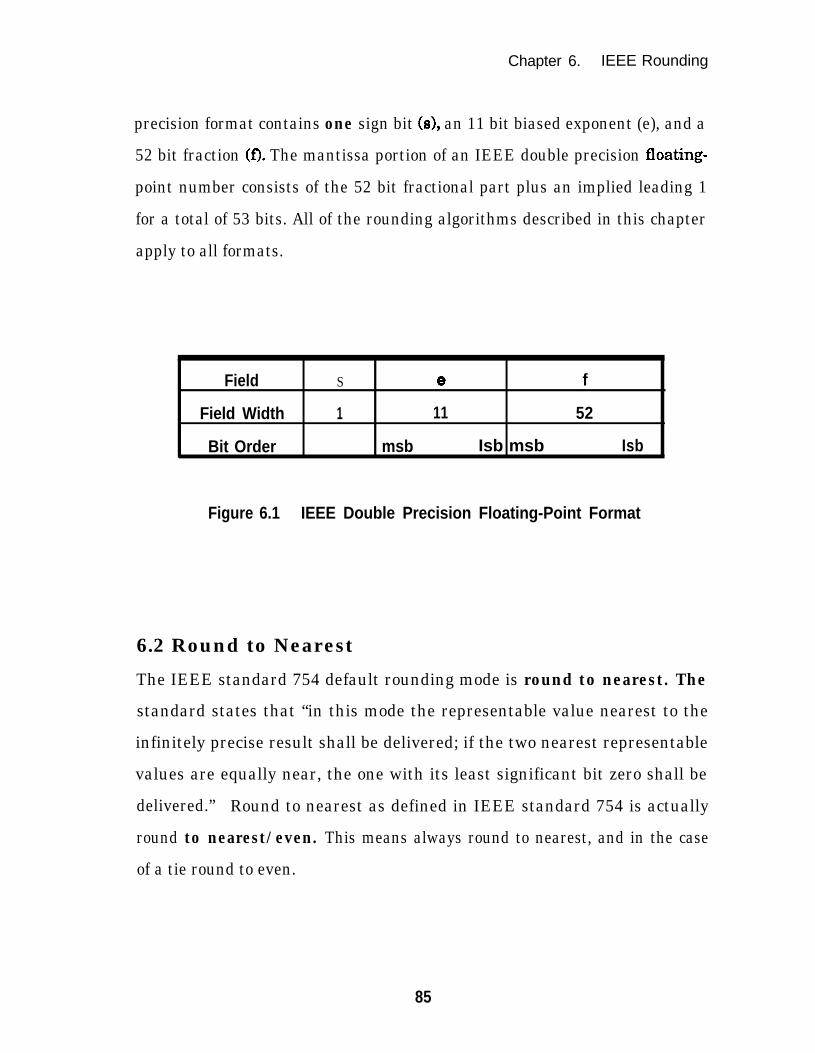
Chapter 6. IEEE Rounding
precision format contains one sign bit (s), an 11 bit biased exponent (e), and a
52 bit fraction (f). The mantissa portion of an IEEE double precision floating-
point number consists of the 52 bit fractional part plus an implied leading 1
for a total of 53 bits. All of the rounding algorithms described in this chapter
apply to all formats.
Field S 8 f
Field Width 1 11 52
Bit Order msb Isb msb Isb
Figure 6.1 IEEE Double Precision Floating-Point Format
6.2 Round to NearestThe IEEE standard 754 default rounding mode is round to nearest. The
standard states that “in this mode the representable value nearest to the
infinitely precise result shall be delivered; if the two nearest representable
values are equally near, the one with its least significant bit zero shall be
delivered.” Round to nearest as defined in IEEE standard 754 is actually
round to nearest/even. This means always round to nearest, and in the case
of a tie round to even.
85
Chapter 6. IEEE Rounding
A conventional rounding system, round to nearest/up, adds l/2 to the least
significant bit (LSB) of the desired result, and then truncates by removing the
bits to the right of the LSB. Bound to nearest/up produces exactly the same
result as round to nearest/even in all cases except when a tie occurs. If theeven result were the smaller value, round to nearest/up would incorrectly
round up. Dealing with the tie case before rounding makes round to
nearest/even more complex and slower than round to nearest/up. For this
reason, the rounding algorithms developed in this chapter will produce a
round to nearest/up result. At the end of the chapter the so-called “sticky”
bit, which identifies the tie case, will be introduced. It will then be shown
how the correct round to nearest/even result (IEEE round to nearest) can be
obtained from the round to nearest/up result by simply forcing the LSB to a 0
in the case of a tie.
6.3 A Simple Round to Nearest/up AlgorithmMost high performance VLSI multipliers use some sort of array or tree
structure to sum the partial products in the mantissa portion of a floating-
point multiply NAL 641. Figure 6.2 shows a flow diagram for the mantissa
handling section of a floating-point multiply unit. This simple round to
nearest/up scheme will be referred to as Algorithm 6.1.
86

Multiply
CPAdd
n bit binary number n bit binary number
Chapter 6. IEEE Rounding
Array, tree, or iterative structure
2n bit product in’carry save form
lWl*1 Carry bits+m0 0 .~ololel lel4@1 Sum bits
n bits
-yyjz-
Normal tRight shift 1 bit
and Increment ram.I@l~l 1.~0~01exponent L /
n bit round tonearest/up result
Figure 6.2 Algorithm 6.1 Data Flow
87
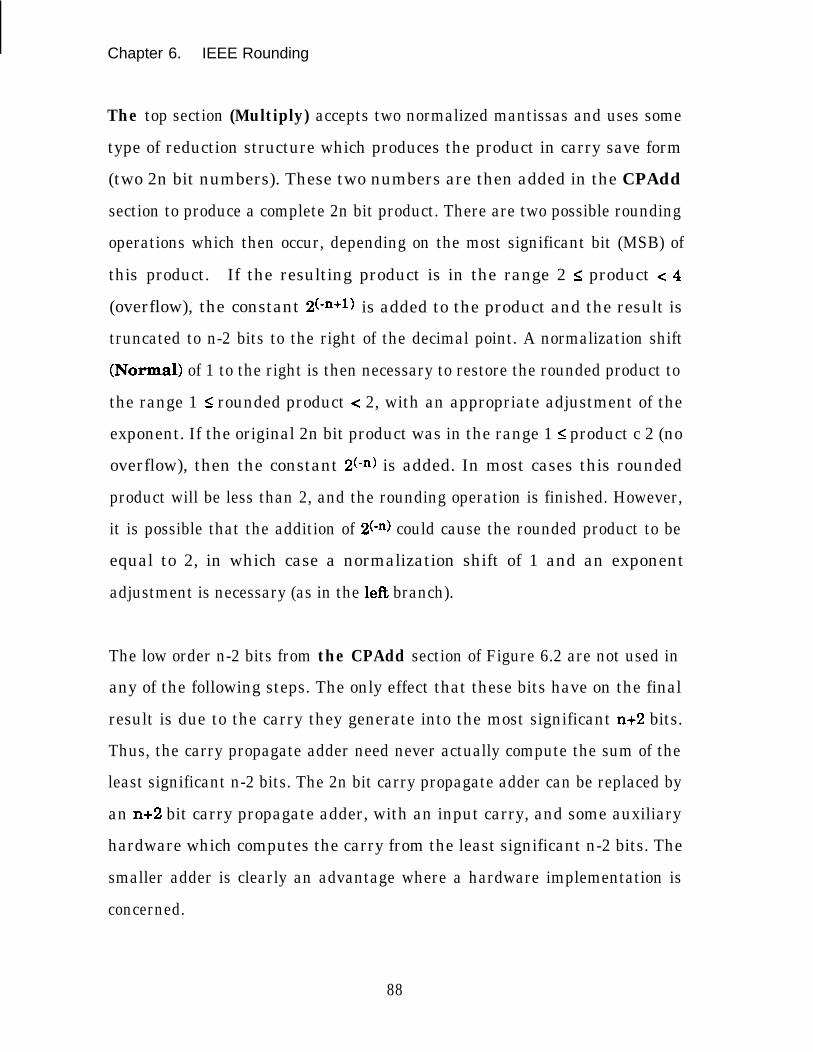
Chapter 6. IEEE Rounding
The top section (Multiply) accepts two normalized mantissas and uses some
type of reduction structure which produces the product in carry save form
(two 2n bit numbers). These two numbers are then added in the CPAdd
section to produce a complete 2n bit product. There are two possible rounding
operations which then occur, depending on the most significant bit (MSB) of
this product. If the resulting product is in the range 2 I product < 4
(overflow), the constant 2(-“+I) is added to the product and the result is
truncated to n-2 bits to the right of the decimal point. A normalization shift
(Ndrmal) of 1 to the right is then necessary to restore the rounded product to
the range 1 I rounded product < 2, with an appropriate adjustment of the
exponent. If the original 2n bit product was in the range 1 I product c 2 (no
overflow), then the constant 2(-n) is added. In most cases this rounded
product will be less than 2, and the rounding operation is finished. However,
it is possible that the addition of 2(-n) could cause the rounded product to be
equal to 2, in which case a normalization shift of 1 and an exponent
adjustment is necessary (as in the left branch).
The low order n-2 bits from the CPAdd section of Figure 6.2 are not used in
any of the following steps. The only effect that these bits have on the final
result is due to the carry they generate into the most significant n+2 bits.
Thus, the carry propagate adder need never actually compute the sum of the
least significant n-2 bits. The 2n bit carry propagate adder can be replaced by
an n+2 bit carry propagate adder, with an input carry, and some auxiliary
hardware which computes the carry from the least significant n-2 bits. The
smaller adder is clearly an advantage where a hardware implementation is
concerned.
88
Chapter 6. IEEE Rounding
Algorithm 6.1 requires two carry propagate additions in series. In section 6.4
Algorithm 6.2 concentrates on computing these additions in parallel, which
significantly increases performance. Finally, in section 6.5 Algorithm 6.3
moves the carry from the lower order bits out of the critical path.
6.4 Parallel Addition SchemesIf an n+2 bit carry propagate adder is used in the CPAdd section of Figure
6.2, then the carry from the lower bits (Gin) will be added at the 2(-“) bit
position. Assuming that no overflow occurred, an additional 2(-“) will be
added to the result in the Round section. The 2(-“) bit position will thus be
called the round bit position, or R bit. The 1 that always gets added to the R
bit position for rounding will be identified as Rin. If no overflow occurs,
adding Cin and Rin to the R bit position will produce the correct round to
nearest/up result.
Now consider the overflow case. The MSB, known as the overflow bit 0, is a
1. By assuming that no overflow would occur, 2(-“) was added for rounding.
If an overflow did occur, then 2(-*+l) should have been added for rounding.
The difference of 2(-“) must be added to correct the rounding. This can be
done by defining a new bit that is added to the 2(-“) bit position in the case of
an overflow. This bit will be called the overflow rounding bit (Rv). The
correct rounding can thus be obtained by simply adding the carry from the
lower order bits (Gin), the rounding bit (Rin), and in the case of an overflow
(Rv), to the R b’t1 position. These bits are shown in Figure 6.3.
89
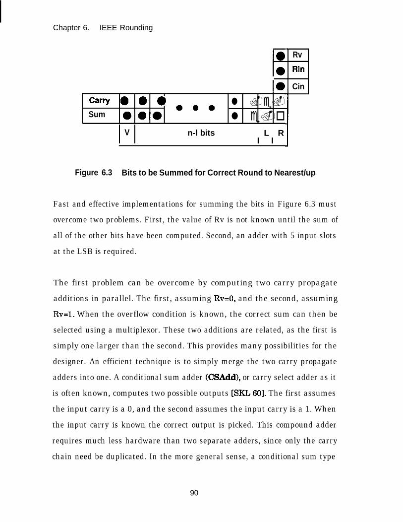
Chapter 6. IEEE Rounding
t@0I.
carry 0 0 0 . . . l .e.Sum 0.0 l e.o
I IV n-l bitsI I
L R
Rv
Rln
Cin
Figure 6.3 Bits to be Summed for Correct Round to Nearest/up
Fast and effective implementations for summing the bits in Figure 6.3 must
overcome two problems. First, the value of Rv is not known until the sum of
all of the other bits have been computed. Second, an adder with 5 input slots
at the LSB is required.
The first problem can be overcome by computing two carry propagate
additions in parallel. The first, assuming Rv=O, and the second, assuming
Rv=l. When the overflow condition is known, the correct sum can then be
selected using a multiplexor. These two additions are related, as the first is
simply one larger than the second. This provides many possibilities for the
designer. An efficient technique is to simply merge the two carry propagate
adders into one. A conditional sum adder (CSAdd), or carry select adder as it
is often known, computes two possible outputs [SKL, 601. The first assumes
the input carry is a 0, and the second assumes the input carry is a 1. When
the input carry is known the correct output is picked. This compound adder
requires much less hardware than two separate adders, since only the carry
chain need be duplicated. In the more general sense, a conditional sum type
90
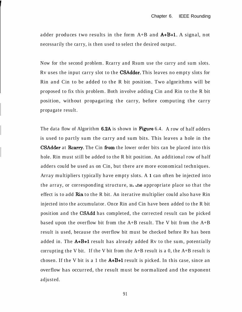
Chapter 6. IEEE Rounding
adder produces two results in the form A+B and A+B+l. A signal, not
necessarily the carry, is then used to select the desired output.
Now for the second problem. Rcarry and Rsum use the carry and sum slots.
Rv uses the input carry slot to the CSAdder. This leaves no empty slots for
Rin and Cin to be added to the R bit position. Two algorithms will be
proposed to fix this problem. Both involve adding Cin and Rin to the R bit
position, without propagating the carry, before computing the carry
propagate result.
The data flow of Algorithm 6.2A is shown in Figure 6.4. A row of half adders
is used to partly sum the carry and sum bits. This leaves a hole in the
CSAdder at Rcarry. The Cin from the lower order bits can be placed into this
hole. Rin must still be added to the R bit position. An additional row of half
adders could be used as on Cin, but there are more economical techniques.
Array multipliers typically have empty slots. A 1 can often be injected into
the array, or corresponding structure, 1~ Lhe appropriate place so that the
effect is to add Rin to the R bit. An iterative multiplier could also have Rin
injected into the accumulator. Once Rin and Cin have been added to the R bit
position and the CSAdd has completed, the corrected result can be picked
based upon the overflow bit from the A+B result. The V bit from the A+B
result is used, because the overflow bit must be checked before Rv has been
added in. The A+B+l result has already added Rv to the sum, potentially
corrupting the V bit. If the V bit from the A+B result is a 0, the A+B result is
chosen. If the V bit is a 1 the A+B+l result is picked. In this case, since an
overflow has occurred, the result must be normalized and the exponent
adjusted.
91
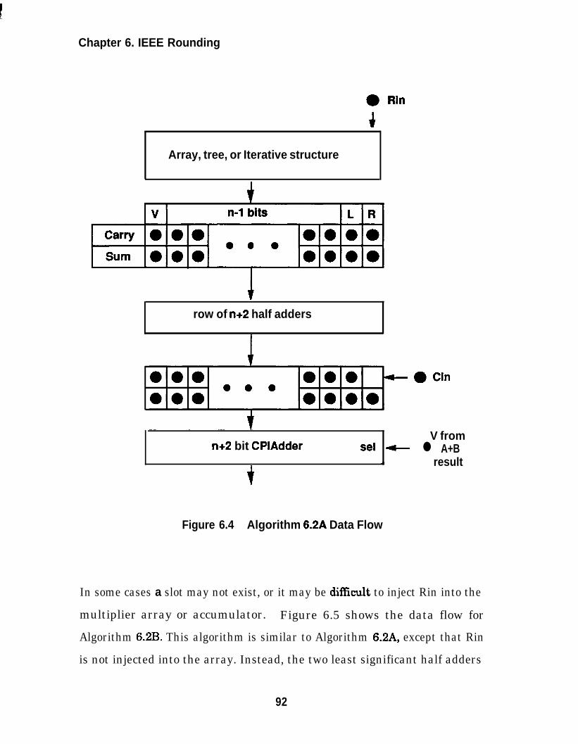
Chapter 6. IEEE Rounding
Array, tree, or Iterative structure
row of n+2 half adders
n+2 bit CPlAdderV from
Se1 - l A+B4 result
Figure 6.4 Algorithm 6.2A Data Flow
In some cases a slot may not exist, or it may be difikult to inject Rin into the
multiplier array or accumulator. Figure 6.5 shows the data flow for
Algorithm 6.2B. This algorithm is similar to Algorithm 6.2A, except that Rin
is not injected into the array. Instead, the two least significant half adders
92

Chapter 6. IEEE Rounding
are replaced with CM’s, providing two additional slots at the L and R bit
positions.23 Rin, which is always a 1, can be combined with Cin and placed
into these empty slots. If Cin equals 0, then a 1 from Rin should be added to
the R bit. If Cin equals 1, then 2 should be added to the R bit position; one
from Rin and one from Cin. Adding 2 to the R bit position is equivalent to
adding 1 to the R+l (L) bit position. The output of the half adder/GSA row
may then be fed to the CSAdder as in Algorithm 6.2A.
row of n half adders
Figure 6.5 Algorithm 6.28 Data Flow
23For simplicity, an entire row of CSA’s could be used, with the unused inputs set to 0.
93

Chapter 6. IEEE Rounding
In the case of a conventional array, the carry from the lower order bits (Gin)
may be determined soon after the carry-save bits, so waiting for Cin before
doing the halfor full additions may not be a problem. Other multipliers may
require additional time to determine the carry from the lower order bits. As
an example, iterating multipliers may require one or more additional cycles
to determine Cin [SAN 89Al. The next section develops a rounding algorithm
which eliminates Cin from the critical path.
6.5 Removing Cin from the Critical PathReferring back to Figure 6.3, five bits must be added at the R bit position.
They are Rv, Rin, Cin, Rcarry, and Rsum. Since Rin is always a 1, the sum of
these five bits can range from 1 to 5. The resulting carry from the R bit to the
L bit will be equal to 0, 1, or 2. Since the CSAdder can only propagate a carry
of 0 or 1 in parallel, the situation may appear hopeless, but this is not the
case.
Knowing that Rin is always a 1 narrowed the range of possible sums from O-5
to l-5. It is possible to further narrow the range of possible sums, and thus
narrow the range of possible carries, by summing some of the bits before the
others are known. Rv is not known until the carry propagate addition is
completed and the V bit is examined. It was also stated that the goal of this
section was to start the carry propagate additions before Cin is known.
Rcarry and Rsum are both known before Rv and Cin. In fact, they are known
at the same time, or before, all of the other carry/save bits, and the carry
propagate additions cannot be started until these bits are known. By looking
94

Chapter 6. IEEE Rounding
at Rin, Rcarry, and Rsum, the possible sum, and possible resulting carries
from the R bit to the L bit, of the 5 bits at the R bit position can be further
narrowed as shown in Table 6.1. For example: if Rcarry = 1, and Rsum = 0
then, the sum of Rsum, Rcarry, Rin, Rv, and Cin must be in the range 2-4.
The possible carry from the R to the L bit will then be in the set (1,2}.
c3 c5 R to L carry
1 1s {%I 1
2 2-4 {Ia3 3-5 11921
where:C3 = Rsum + Rcany + Rinx5 = Rsum + Rcarry + Rin + Rv + CinR to L carry = Possible carry from R to L
Table 6.1 Carry Propagation from R to L
From Table 6.1 it can be seen that summing Rin, Rsum, and Rcarry limits the
possible carries into the L bit to one of two sets: (0,l) or {1,2). Within each set
the carry differs by exactly 1; therefore, the set of possible rounded results
from the L bit up can differ by at most 1. This is important because the
CSAdder computes results in the form A+B and A+B+l. In addition, since
the R bit is not part of the final correctly rounded result, it need not be
included in the carry propagate addition. Knowing the correct carry set
yields one of two possible cases:
95
Chapter 6. IEEE Rounding
Case 1: The carry set is {OJ).
In this case either a 0 or a 1 must be added to the L bit
position. Since the CSAdder directly computes results in the
form A+B and A+B+l, both possible correct results are
computed. If the actual carry is a 0 the A+B result is selected,
with the A+B+l result selected if the carry is a 1.
Case 2: The carry set is {1,2).
In this case either a 1 or a 2 must be added to the L bit
position. Since a CSAdder cannot compute A+B+2, a row of
half adders should be used, providing a slot to add 1 to the L
bit position. This leaves either a 0 or a 1 to be added to the L
bit position. This is precisely case 1 and should be handled as
such.
Referring to Table 6.1, the carry set (0,l) (Case 1) is chosen only if C3 = 1.
Since Rin is always 1, a logical OR on Rcarry and Rsum can be used to
differentiate between Case 1 and Case 2. Placing the output of this OR gate
into the empty slot created by a row of half adders will correctly add a 1 to the
L bit for Case 2 and a 0 for Case 1 (see Figure 6.6).
96

Chapter 6. IEEE Rounding
V n-l bits
Carry 0 0 0 . . .
Sum * 0 l
L R
I Half add on n+l carry save bits I I
l ee em 40.0 l 0 . l *o
n+l bit CSAdd
t
Result selectlogic basedupon Rln,Rcarty, Rsum,Rv, Gin.
Figure 6.6 Algorithm 6.3 Data Flow
Once both possible results have been computed, the correct one must be
picked. Cin should now be known; Rv, however, is not. The V bit from the
A+B output is not automatically the correct value to use for Rv, as it was in
Algorithm 6.2. The reason is that the other bits may have already
determined that the A+B+l result should be chosen, regardless of the value of
the V bit. To determine the correct V bit to use for Rv, a preliminary A+B or
A+B+l value should be chosen based upon the X5 column of Table 6.2,
assuming that Rv=O. The V bit of the selected output will be the correct V bit
to assign to Rv. The value of C5 should then be recalculated using the actual
Rv, and the correct A+B or A+B+l result selected. The normalization and
exponent adjustment is the same as in Algorithm 6.2.
97

Chapter 6. IEEE Rounding
x3
I
I
1
2
2,3
2,3
2.3
5I
2
3
2
3
4
5
RtoLcarry
0
I
I
output
A+B
A+B+l
A+B+I
A+B
A+B
A+B+I
A+B+I
Case I
Case 2
where:x3 = Rsum + Rcarry + RinC5 = Rsum + Rcarry + Rin + Rv + CinR to L carry = Possible carry from R to LOutput = The CSAdder output to be selected
Table 6.2 CSAdder Output Selection
6.6 IEEE Rounding Modes
6.6.1 Round Toward W, IQ), and Zero
In addition to round to nearest, the default rounding mode, IEEE standard
754 defines three other optional rounding modes. These “directed” rounding
modes are round toward +w, round toward -00 and round toward zero. Once
round to nearest has been implemented, the other rounding modes are
relatively simple. To begin with, consider round toward zero. This is simply
98
Chapter 6. IEEE Rounding
a truncation. All of the previous algorithms will work, except the Rin and Rv
bits will now be 0.
Now let’s look at round toward +m. The standard states that “when rounding
toward += the result shall be the format’s value (possible +M) closest to and
no less than the infinitely precise result”. Basically, what this says is that in
the case of a positive result, if all the bits to the right of the LSB of the
desired result are 0, then the result is correct. If any of these bits are a 1, (i.e.
R=l or sticky=l), then a 1 should be added to the LSB of the result. If the
result is negative it should be truncated. When rounding toward -= the exact
opposite holds. The direct rounding algorithms can be summarized as
follows:
Round toward ZeroTruncate
Round toward +-if sign = positive
if any bits to the right of the result LSB = 1Add 1 to result
elseTruncate at LSB
if sign = negativetruncate at LSB
Round toward --if sign = negative
if any bits to the right of the result LSB = 1Add 1 to result
elseTruncate at LSB
if sign = positivetruncate at LSB
99
Chapter 6. IEEE Rounding
6.6.2 Obtaining The IEEE Round to Nearest Result
It was stated earlier that round to nearest/up produces exactly the same
result as round to nearest/even, except when a tie occurs. A tie can only occur
when the result is exactly half way between two numbers of representable
precision. For example:
37.25xMc Raw number to be rounded
Add 0.05 to round to nearest /up+0.05
37.30 SUm
37.3 Truncated - Final rounded Result
If the X’s are all zeros, then 37.25000 is exactly half way between 37.2 and
37.3. In this case round to nearest/up produces a different result than round
to nearest/even. There are only two cases to be considered. Either all of the
X’s are 0, or they are not. The bit which distinguishes between these cases is
referred to as the sticky bit. This bit is a 0 ifall of the X’s are 0, and 1 if any
of the x’s are non-zero.
To produce the correct round to nearest/even result from the unrounded
result, a 1 is potentially added to the round bit. The bit (E) to be added to the
round bit (R) for correct IEEE round to nearest is based upon the L, R, and
sticky (S) bits as shown in Table 6.3.
100

Chapter 6. IEEE Rounding
Before Rounding
L R S
X 0 0
X 0 I
0 I 0
I I 0
X 1 1
Add to R bit
E U
d I
d I
0 I
I I
1 I
L After Rounding
LE LlJ
X X
X X
0 I
0 0
Tz z
where:E = Bit added to R bit for correct round to nearest/even.U = Bit added to R bit for correct round to nearest/up.
LE = The L bit after round to nearest/even.LU = The L bit after round to nearest/up.d = Don’t care. E can not effect L,.
Table 6.3 Round to Nearest/even versus Round to Nearest/up
In contrast, round to nearest/up assumes that the bit to be added to the R bit
for correct rounding (U) is always a 1. The only case where the round to
nearest/up bit (U) will produce a different result from the round to
nearest/even bit (E) is shown in row 3 of Table 6.3, where E=O, and U=l. In
this case round to nearest/up changed the L bit from a 0 (L=O) to a 1 (LE=~),
while round to nearest/even left the L bit unchanged (Lu=O). The important
thing to notice is that when round to nearest/up changed the L bit to a 1, the
1 was not propagated. As such, only the L bit was effected. This means that
the correct round to nearest/even result can be obtained from the round to
nearest/up result by restoring the L bit to a 0.
101
Chapter 6. IEEE Rounding
By assuming that the round bit will be a 1, the round to nearest/up
algorithms have an advantage over the round to nearest/even methods in that
the carry propagate addition can take place before the sticky bit has been
computed. This means that the round to nearest/up result can be obtained
using any of the methods presented in this paper. The correct IEEE round to
nearest result can then be obtained by observing only the L, R, and sticky
bits, and forcing the L bit to 0 if required. Care should be taken, however, as
operations such as right shifting in the event of an overflow, and adding Rv
and Rin, can change the position and/or value of the S, L, and R bits.
6.7 Computing the Sticky bit
6.7.1 A Simple Method to Compute the Sticky Bit
The first method for determining the sticky bit is conceptually the simplest,
as it stems from the very definition of the sticky bit. Recall that the sticky bit
was defined to be equal to 0 if the value of all of the bits to the right of the
round bit is 0. To determine the sticky bit, begin with a carry propagate
addition on all of the bits. The sticky bit (S) will be the OR of all of the bits to
the right of the R bit. This method is quite simple in concept, and is often
used in practice. One drawback is that a full carry propagate addition,
followed by a logical OR, must be done on all of the lower order carry save
bits.
102
Chapter 6. IEEE Rounding
6.7.2 Computing Sticky From the Input Operands
The sticky bit may also be computed directly from the inputs to be multiplied,
bypassing the multiply array completely. The number of trailing zeros in the
binary number X*Y is exactly equal to the number of trailing zeros in X plus
the number of trailing zeros in Y.24 The trailing zeros in X and Y can be
counted and summed while the multiply is taking place. If the sum is greater
than the sum of bits to the right of the round bit, then the sticky bit is a 0.
The advantage of using this method is that the sticky bit can be computed in
parallel with the actual multiplication, removing the sticky bit from the
critical path.
6.7.3 Computing Sticky From the Carry-Save Bits
The third method depends upon all of the partial products being positive (i.e.,
no Booth encoding has been used). Given this assumption, a simple logical
OR on the carry-save form of the bits to the right of the round bit wili
yield the correct sticky bit.
This simple ORing of the carry save bits works for the following reason. If
the 2n bit carry save result is scanned from right to left, the first non-zero
carry/sum pair will contain a single 1. That is, either the carry or the sum
will be a 1 but not both. This single one could not generate a carry during a
2%Yhe number of trailing zeros in the product is exactly equal to the sum of the trailing zerosin the operands, for any representation in which the base is prime. This is true becauseprime numbers cannot be factored. Non-prime bases can be factored; therefore, the numberof trailing zeros in the product can be greater than the sum of the trailing zeros in theoperands. As an example, in base 10 if the least signifkant non-zero bits in the operandswere 2 and 5, respectively, an additional zero would be created, and the number of trailingzeros in the product is larger than the sum of the trailing zeros in the operands.
103
Chapter 6. IEEE Rounding
carry propagate addition, and since all of the bits to its right are zero, there is
no carry to propagate. This will cause the single 1 to remain in its current
position. If this position is to the right of the R bit, the sticky bit will be a 1.
To see why this is true, refer to Figure 6.7. This figure shows a section of the
partial products for the multiplication of A l B. Each row represents a single
partial product which will be generated and later summed to form the carry
save form of the final product. AOBO represents the partial product
represented by the logical AND of bit A0 with bit BO, and so on.
ASBO A4BO A380 A2BO Al BO AOBO
A4Bl A3Bl A2Bl AlBV’ AOBl/’A3B2 A2B2 Al 82 A082
A2B3 AlB3 AOB3
Al B4 AOB4
AOB5
Figure 6.7 Summation of Partial Products
Assume A2B2 in column 4 is a 1, and column 4 is the first column in which a
1 appears. Since A2 is a 1, Bl and BO must both be 0, or there would be a 1
in an earlier column formed by A2Bl in column 3, row 1, or A2BO in column
2, row 0. All products above A2B2 in column 4 contain either a Bl or a BO
and thus must be 0. Looking across row 2, B2 is a 1. This means Al and A0
104
Chapter 6. IEEE Rounding
must both be zero, or a 1 would exist in columns 3 or 2. All products below
A2B2 in column 4 contain either Al or AO, and thus must also be 0.
Therefore, A2B2 is the only non-zero partial product in this column. This can
easily be generalized to any element in any column, proving that the first
column in which a 1 exist will contain a single 1.
.6.8 Rounding Hardware for Iterative Structures
All floating-point multipliers must compute the sticky bit, and the carry from
the lower order bits, for correct IEEE rounding. Conventional linear array
multipliers reduce partial products at a relatively slow rate, which is
proportional to the operand size. By adding a few extra rows of CSA’s, it is
possible for linear arrays to perform a ripple carry propagate addition
without significantly degrading performance. Tree structures reduce partial
products at a much faster rate, proportional to the log of the operand size.
Summing the lower order bits at the FI. .z1;? rate as the upper order bits
requires the width of the tree to be doubled. That is, for an N bit operand a
2N bit wide tree is required.
An iterative 4-2 multiplier has an advantage over the full tree multiplier in
that only a partial tree is used. This smaller tree means that the additional
width required to sum the lower order bits is less than the full tree case.
That is, if two N bit operands were multiplied using a K bit partial tree, an
N+K bit wide array would be required as opposed to the 2N bit wide array for
a full tree. As an example, assume a 64 X 64 bit mantissa is to be multiplied
(N=64) using an 8 input 4-2 tree (K=8), with a 4-2 carry save accumulator.
105
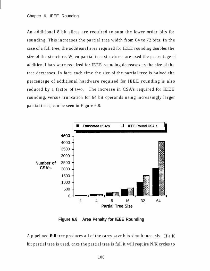
Chapter 6. IEEE Rounding
An additional 8 bit slices are required to sum the lower order bits for
rounding. This increases the partial tree width from 64 to 72 bits. In the
case of a full tree, the additional area required for IEEE rounding doubles the
size of the structure. When partial tree structures are used the percentage of
additional hardware required for IEEE rounding decreases as the size of the
tree decreases. In fact, each time the size of the partial tree is halved the
percentage of additional hardware required for IEEE rounding is also
reduced by a factor of two. The increase in CSA’s required for IEEE
rounding, versus truncation for 64 bit operands using increasingly larger
partial trees, can be seen in Figure 6.8.
Number ofCSA’s
n Tnmcated CSA’s q IEEE Round CSA’s
4000
3500
3000
2500
2000
1500
1000
500
02 4 8 16 32 64
Partial Tree Size
Figure 6.8 Area Penalty for IEEE Rounding
A pipelined full tree produces all of the carry save bits simultaneously. If a K
bit partial tree is used, once the partial tree is full it will require N/K cycles to
106

Chapter 6. IEEE Rounding
produce all of the carry save bits. Once the accumulator contains valid data,
K bits will “fall off the end, on each cycle. The first K bits must be examined
to see if they generate a carry to the higher order bits. On each additional
cycle, the next higher order K bits must be examined to see if they generate a
carry, or propagate the carry from the lower order bits which preceded. The
iterative structure has the advantage over a full tree in that only K bits need
to be examined each cycle, where the entire N bits must be examined at one
time for the full tree. This saves hardware inversely proportional to the
partial tree size. The carry circuit must be pipelined, since only K out of the
N bits are generated each cycle. (see Figure 6.9) The latch, which
accumulates the carry, must be reset on the first carry accumulation cycle, to
prevent an erroneous carry from being propagated. Deeper pipelining may
also be required, as the piped carry stage must operate faster than the basic
single 4-2 stage.
Ck Sk CD 0 e co so
I Cout K bit carry ckt Cin 1
Carry
Figure 6.9 Piped Carry Circuit
107
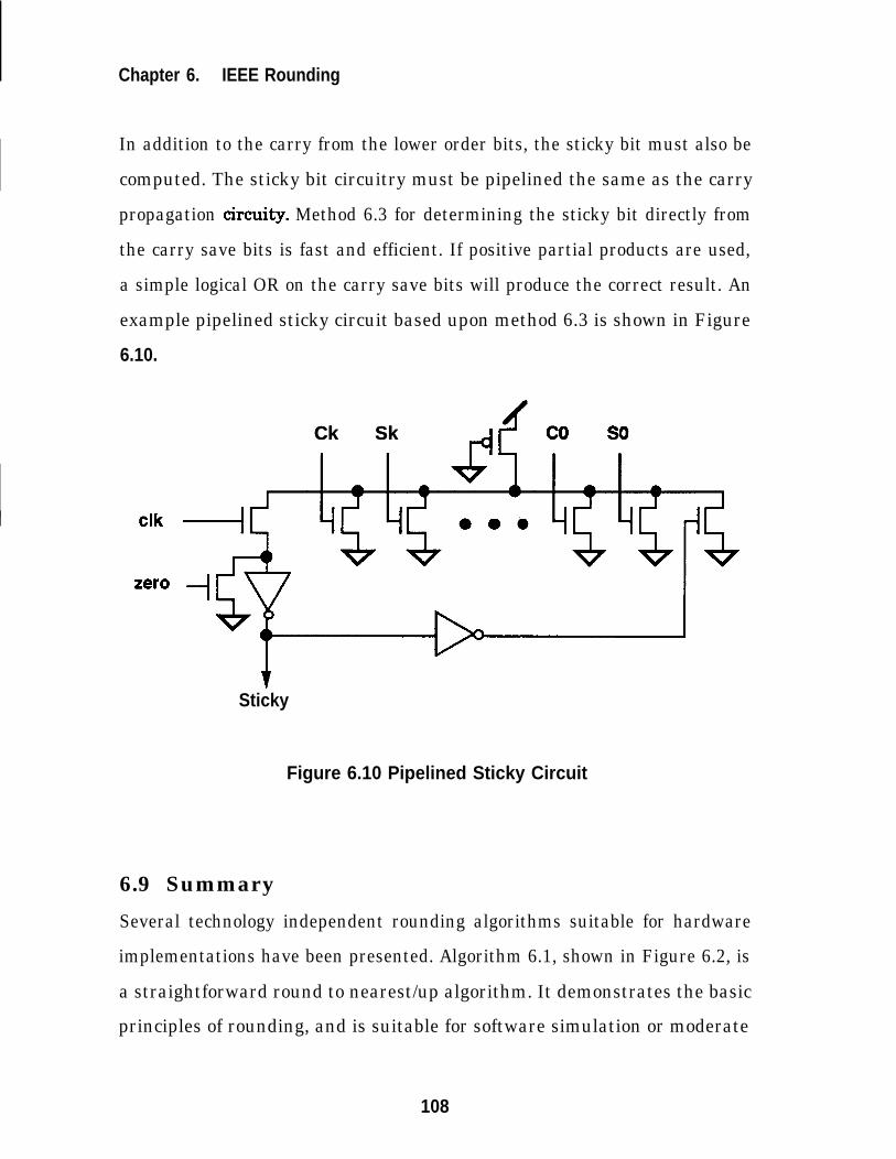
Chapter 6. IEEE Rounding
In addition to the carry from the lower order bits, the sticky bit must also be
computed. The sticky bit circuitry must be pipelined the same as the carry
propagation circuity. Method 6.3 for determining the sticky bit directly from
the carry save bits is fast and efficient. If positive partial products are used,
a simple logical OR on the carry save bits will produce the correct result. An
example pipelined sticky circuit based upon method 6.3 is shown in Figure
6.10.
Ck SkCk Sk d P co so
tSticky
Figure 6.10 Pipelined Sticky Circuit
6.9 SummarySeveral technology independent rounding algorithms suitable for hardware
implementations have been presented. Algorithm 6.1, shown in Figure 6.2, is
a straightforward round to nearest/up algorithm. It demonstrates the basic
principles of rounding, and is suitable for software simulation or moderate
108
Chapter 6. IEEE Rounding
performance hardware implementation. Algorithms 6.2 and 6.3 are better
suited for high performance VLSI multipliers. While Algorithm 6.1 requires
two series carry propagate additions, algorithms 6.2 and 6.3 use a parallel
carry propagate addition scheme. Algorithm 6.2A (Figure 6.4) would be a
likely choice for most conventional array or full tree multipliers. Algorithm
6.2B (Figure 6.5) would be preferable if a blank slot does not exist in the
array for summing in the rounding bit (Rin). Though slightly more complex
than the other methods, Algorithm 6.3 (Figure 6.6) is best suited for iterative
multipliers, or any multiplier where the carry from the lower order bits is in
the critical path. By using the sticky bit, any of the round to nearest/up
results can be corrected to comply with IEEE standard 754 rounding.
Finally, three methods for determining the sticky bit were presented. The
first method originates directly from the definition of the sticky bit. The
second method allows the sticky bit to be determined from the input operands
in parallel with the actual multiplicaticn. The third method represents a new
fast and efficient technique for determining the sticky bit from the carry save
bits.
For iterative SPIM type multipliers, rounding Algorithm 6.3, combined with
Method 6.3 for determining the sticky bit, provides a fast and area efficient
technique for IEEE rounding. A block diagram for an N bit multiplier using a
K bit wide partial tree is shown in Figure 6.11. The shaded area represents
the additional hardware required for IEEE rounding. The partial tree is N
bits wide for the operands, plus two bits for the V and R bits, plus an
additional K bits required for IEEE rounding. The Piped Carry and Sticky
logic shown in figures 6.9 and 6.10 can be used to determine the Cin and
109
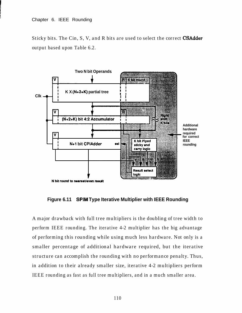
Chapter 6. IEEE Rounding
Sticky bits. The Cin, S, V, and R bits are used to select the correct CSAdder
output based upon Table 6.2.
Two N bit Operands
ClkII
K X (N+2+K) partial tree i II I
I N+l bit CPlAdder
Additionalhardwarerequiredfor correctIEEEroundlng
Figure 6.11 SPIM Type Iterative Multiplier with IEEE Rounding
A major drawback with full tree multipliers is the doubling of tree width to
perform IEEE rounding. The iterative 4-2 multiplier has the big advantage
of performing this rounding while using much less hardware. Not only is a
smaller percentage of additional hardware required, but the iterative
structure can accomplish the rounding with no performance penalty. Thus,
in addition to their already smaller size, iterative 4-2 multipliers perform
IEEE rounding as fast as full tree multipliers, and in a much smaller area.
110
Chapter 7
Summary
7.1 SummaryThis thesis has presented a new multiplier architecture which is both faster
and smaller than linear array multipliers. The high performance is obtained
by using a new tree structure, the 4-2 tree. The 4-2 tree is symmetric and far
more regular than other multiplier trees while offering comparable
performance, making it better suited for VLSI implementations. To reduce
area, a partial, pipelined 4-2 tree is used with a 4-2 carry-save accumulator
placed at its outputs to sum the partial products as they are generated. By
using a partial tree and iteratively accumulating the partial products, the
performance advantages of trees is obtained in a much smaller size.
111
Chapter 7. Summary
To obtain maximum performance the 4-2 tree must be clocked at a rate equal
to the combinational delay of the 4-2 stages. To achieve such tight control on
the fast iterative multiplier clock, a stoppable on-chip clock generator was
presented which can accurately match, and track, the delay of the 4-2
multiplier logic. Using a stoppable on-chip clock generator provides several
advantages over using an external system clock. These include: 1) better
matching of the 4-2 combinational delay, yielding higher performance; 2) the
ability to track 4-2 performance over variations in temperature, supply
voltage, and processing; 3) the elimination of clock synchronization problems.
Performance limits based upon current and future technologies were also
discussed. For current technologies, the clock frequency is limited by the 4-2
carry-save accumulator delay. Although performance will eventually be
limited by the clock lines, this should not be the case until technologies well
below 0.5 v have been achieved with clock frequencies approaching 1 GHz.
The new multiplier architecture developed in this dissertation is useful for
implementing both integer and floating-point multipliers. To demonstrate its
usefulness for floating-point, several high-performance rounding algorithms
which adhere to the IEEE standard for floating-point arithmetic were
presented. In addition, a new method for computing the sticky bit directly
from the carry-save form of the result was discussed. It was then shown that
iterative 4-2 multipliers require less additional rounding hardware than full
trees, with no performance penalty.
A test chip, the Stanford Pipelined Iterative Multiplier (SPIM), was
fabricated to demonstrate the feasibility of iterative 4-2 multipliers. SPIM
implements the 64 bit mantissa portion of a double extended precision
112
Chapter 7. Summary
floating-point multiply. SPIM was fabricated in a 1.6 pm CMOS process and
ran at an internal clock frequency of 85 MHz. The latency for a 64 X 64 bit
fractional multiply is under 120 ns. SPIM contains 41,000 transistors with
an array size of 2.9 X 5.3 mm. By using a partial, pipelined 4-2 tree and
accumulator, SPIM provides over twice the performance of a comparable
conventional full array at l/4 of the silicon area. The SPIM chip proved that
the new architecture works, and is smaller and faster than current multiplier
architectures.
7.2 Future WorkAn obvious continuation of this work would be to implement an IEEE
compatible floating-point multiplier in a more aggressive CMOS technology.
A clock generator clocking a 4-2 adder at 400 MHz was implemented in a 0.8
pm CMOS technology, demonstrating the potential performance of iterative
4-2 multipliers. Investigations into other technologies such as ECL and GaAs
might also prove interesting. Size and power constraints currently prohibit
full linear array or tree implementations in either of these technologies. Such
implementations would also further the study of high-speed clocking.
The ability to construct very small high performance multipliers provides
many other interesting possibilities. A double precision IEEE multiplier
could be placed on the same chip with an existing RISC or CISC processor.
Multiplication intensive applications, such as DSP or graphics, could benefit
significantly from several high performance multipliers on the same chip. A
single very high throughput multiplier, or several multipliers working in
113
Chapter 7. Summary
parallel on the same chip, could open up new possibilities such as single chip
video signal processors. Further investigation into communications between
iterative 4-2 multipliers and other hardware, or between several 4-2
multipliers, should also continue as it may produce better system interfaces.
114

References
[AND 671
[BEN 891
[BOO 511
[CAV 841
[CHA 861
[COO 801
[DAD 651
[DIL 881
[ELK 871
[GAM 861
[GON 831
S. F. Anderson, J. G. Earle, et al., “The IBM system360 Model91: Floating-Point Execution Unit”, IBM Journal, vol. 11, no. 1,pp. 34-53, January 1967.
B.J. Benschneider, et. al., “A 50 MHz Uniformly Pipelined 64bFloating-Point Arithmetic Processor”, IEEE Int. Solid-StateCircuits conf., pp. 50-51, February 1989.
A. D. Booth, “A Signed Binary Multiplication Technique”, Qt. J.Mech. Appl. Math., vol. 4, Part 2,195l.
J. F. Cavanagh, “Digital Computer Arithmetic Design andImplementation”, McGraw-Hill, 1984.
D. M. Chapiro, “Globally-Asynchronous Locally-SynchronousSystems”, Ph. D. Thesis, Stanford University, October 1986.
J. J. Coonen, “An Implementation Guide to a Proposed Standardfor Floating-Point Arithmetic”, Computer Magazine vol. 13, no.1, January 1980.
L. Dadda, “Some Schemes for Parallel Multipliers,” AltaFrequenza, vol. 34, no. 5, pp. 0+&-356, March 1965.
D. L. Dill, Trace Theory for Automatic Hierarchical Verificationof Speed-Independent Circuits”, Ph. D. Thesis, Carnegie MellonUniversity, CMU-CS-88-119, February 1988.
B. Elkind, J. Lesser& J. Peterson, and G. Taylor, “A Sub 10 nsBipolar 64 Bit Integer/Floating Point Processor Implemented onTwo Circuits”, IEEE Bipolar Circuits and Technology Meeting,pp. 101-104, September 1987.
A. Gamal, et. al., “A CMOS 32b Wallace Tree Multiplier-Accumulator”, ISSCC Digest of Technical Papers, ISSCCProceedings, pp. 194-l 95, February, 1986.
N. Goncalves and H. De Man, “NORA: A Racefree DynamicCMOS Technique for Pipelined Logic Structures”, IEEE Journalof Solid State Circuits, vol. SC-18, pp. 261-266,1983.
References
[GOS 831 J. B. Gosling, %ome Tricks of The (Floating-Point) Trade”, IEEE6th Symposium on Computer Arithmetic, pp. 218-220,September 1983.
[HAR 871 Y. Harata, et. al., “A High-Speed Multiplier Using a RedundantBinary Adder Tree”, IEEE Journal of Solid-State Circuits, vol.SC-22, no. 1, February 1987.
[HEN 851 D. A. Henhn, M. T. Fertsch, M. Mazin, and E. T. Lewis, “A 16Bit X 16 Bit Pipelined Multiplier Macrocell”, IEEE Journal ofSolid-State Circuits, vol. SC-20, no. 2, April 1985.
[HWA 791 K. Hwang, “Computer Arithmetic: Principles, Architecture, andDesign”, New York, John Wiley & Sons, 1979.
[IEE 851 “IEEE Standard for Binary Floating-Point Arithmetic”,ANSI/IEEE Std 754-1985, New York, The Institute of Electricaland Electronics Engineers, Inc., August 12,1985.
[JOH 831 K. Johnsen, “An IEEE Floating Point ArithmeticImplementation”, IEEE 6th Symposium on ComputerArithmetic, pp. 130-135, September 1983.
[JOU 881 N. P. Jouppi, ‘MultiTitan: Four Architecture Papers”, WRLResearch Report, April 1988.
[KAW 881 S. Kawahito, et. al., “A 32 X 32-bit Multiplier Using Multiple-Valued MOS Current-Mode Circuits”, IEEE Journal of Solid-State Circuits, vol. 23, no. 1, February 1988.
[LIE 891 B. K. Liew, N. W. Chung, and C. Hu, “ElectromigrationInterconnect Lifetime Under AC and Pulse DC Stress”, IEEE27th Annual Reliability Physics conference proceedings, pp. 215-219, April ll-13,1989.
[LU 881 P. Y. Lu, et al., “A 30-MFLOP 32b CMOS Floating-PointProcessor”, IEEE Solid-State Circuits Conference proceedingsvol. XXXI, pp. 28-29, February 1988.
MCA 861 W. McAllister and D. Zuras, “An nMOS 64b Floating Point ChipSet”, IEEE Int. Solid-State Circuits conf., pp. 34-35, February1986.
MCG 871 M. S. McGregor, P. B. Denyer, and A. F. Murray “A Single-PhaseClocking Scheme for CMOS VLSI”, Proceedings of the 1987Stanford Conference on Advanced Research in VLSI, pp. 75-95,Cambridge, Massachusetts, The MIT Press, 1987.
116
[MEA 801
[MEN 881
[MEN 891
cMII~651
[NOL 861
[NOI 831
[PEN 871
[SAN 881
[SAN 89A]
[SAN 89B]
[SHE 781
[SKL 601
[UNG 691
References
C. Mead, and L. Conway, ‘Introduction to VLSI Systems”,Massachusetts, Addison-Wesley, 1980.
T. Meng, “Asynchronous Design for Digital Signal ProcessingArchitectures”, Ph. D. Thesis, University of California atBerkeley, November 1988.
T. Meng, “Design of Clock-Free Asynchronous Systems for RealTime Signal Processing”, Proceedings of IEEE ICASSP, May1989.
R. E. Miller, “Switching Theory”, John Wiley & Sons, Inc., NewYork, 1965.
T. G. Noll, D. Schmitt-Landsiedel, H. Klar, and G. Enders, “APipelined 330-MHz Multiplier”, IEEE Journal of Solid-StateCircuits, vol. SC-21, no. 3, June 1986.
D. C. Noice, “A Clocking Discipline for Two-Phase DigitalIntegrated Circuits”, Ph. D. Thesis, Stanford University,Stanford, California, January 1983.
V. Peng, S. Sanudrala, M. Gavrielov, “On The Implementation ofShifters, Multipliers, and Dividers in VLSI Floating PointUnits”, IEEE 8th Symposium on Computer Arithmeticproceedings, pp. 95-102, May 1987.
M. Santoro, and M. Horowitz, ‘A Pipelined 64X64b IterativeArray Multiplier”, IEEE Int. Solid-State Circuits conf., pp. 3536, February 1988.
M. Santoro, and M. Horowtz, “SPIM: A Pipelined 64X64-bitIterative Multiplier”, IEEE Zournal of Solid-State Circuits, vol.24, no. 2, April 1989.
M. Santoro, G. Bewick, and M. Horowitz, “Rounding Algorithmsfor IEEE Multipliers”, IEEE 9th Symposium on ComputerArithmetic proceedings, pp. 176-l 83, September 1989.
D. T. Shen and A. Weinberger, “4-2 Carry-Save AdderImplementation Using Send Circuits”, IBM Technical DisclosureBulletin, vol. 20, no. 9, February 1978.
J. Sklansky, ‘Conditional Sum Addition Logic”, Trans. IRE, vol.EC-g, no. 2, pp. 226-230, June 1960.
S. H. Unger, ‘Asynchronous Sequential Switching Circuits”,Wiley-Interscience. John Wilev & Sons. Inc.. New York. 1969.
117

References
IWAL 641 C. S. Wallace, ‘A Suggestion for Fast Multipliers”, IEEETransactions on Electronic Computers, vol. EC-13, pp. 14-17,February 1964.
IWAR 821 Frederick A. Ware, William H. McAllister, John R. Carlson, DanK. Sun, and Richard J. Vlach, “64 Bit Monolithic Floating PointProcessors”, IEEE Journal of Solid-State Circuits, vol. SC-17, no.5, October 1982.
CWAS 821 S. Waser, and M. J. Flynn, ‘Introduction to Arithmetic forDigital Systems Designers”, New York, CBS Publishing, 1982.
IWL 871 T. E. Williams, M. A. Horowitz, R. L. Alverson, and T. S. Yang,“A Self-Timed Chip for Division”, Proceedings of the 1987Stanford Conference on Advanced Research in VLSI, pp. 75-95,Cambridge, Massachusetts, The MIT Press, 1987.
[YOH 731 J. M. Yohe, “Roundings in Floating-Point Arithmetic”, IEEETransactions on Computers, vol. C-22 no. 6, pp. 577-586, June1973.
[YUA 891 J. Yuan, and C. Svensson, “High-Speed CMOS CircuitTechnique”, IEEE Journal of Solid-State Circuits, vol. 24, no. 1,February 1989.
[ZUR 861 D. Zuras, and W. McAllister, “Balanced Delay Trees andCombinatorial Division in VLSI”, IEEE Journal of Solid-StateCircuits, vol. SC-21, no. 5, October 1986.
118