datasheet for the tps65023 - texas instruments - ti. · pdf filesystem platform tps6502x dcdc1...
TRANSCRIPT
System Platform
TPS6502x
DCDC1
DCDC2
DCDC3
LDO1
LDO1
Example SoC
CORE
1.8-V IO Domain
Memory
3.3-V IO Domain
Memory
22 µF
22 µF
22 µF
2.2 µH
2.2 µH
2.2 µH
2.2 µF
2.2 µF
2.2 µF
BACKUP
Enables andVout
Select
DCDC1_ENDCDC2_ENDCDC3_EN
LDO_EN
DEFDCDC1DEFDCDC2DEFDCDC3
+±
+±
R1
R2
Monitored Voltage1
R3
R4
Monitored Voltage2
RESPWRON System Reset
PWRFAIL
LOWBATT
RTC AND VBACKUP
Peripherals
Product
Folder
Order
Now
Technical
Documents
Tools &
Software
Support &Community
ReferenceDesign
An IMPORTANT NOTICE at the end of this data sheet addresses availability, warranty, changes, use in safety-critical applications,intellectual property matters and other important disclaimers. PRODUCTION DATA.
TPS65023, TPS65023BSLVS670L –JUNE 2006–REVISED MAY 2018
TPS65023x Power Management IC (PMIC) With 3 DC/DCs, 3 LDOs, I2C Interface and DVS
1
1 Features1• 1.7-A, 90% Efficient Step-Down Converter for
Processor Core (VDCDC1)• 1.2-A, Up to 95% Efficient Step-Down Converter
for System Voltage (VDCDC2)• 1.0-A, 92% Efficient Step-Down Converter for
Memory Voltage (VDCDC3)• 30-mA LDO and Switch for Real Time Clock
(VRTC)• 2 × 200-mA General-Purpose LDO• Dynamic Voltage Management for Processor Core• Preselectable LDO Voltage Using Two Digital
Input Pins• Externally Adjustable Reset Delay Time• Battery Backup Functionality• Separate Enable Pins for Inductive Converters• I2C-Compatible Serial Interface• I2C™ Setup and Hold Timing:
– TPS65023: 300 ns– TPS65023B: 100 ns
• 85-μA Quiescent Current• Low Ripple PFM Mode• Thermal Shutdown Protection• 40-Pin, 5-mm × 5-mm WQFN Package
2 Applications• Digital Media Players• Internet Audio Players• Digital Still Cameras• Smart Phones• Supply DaVinci™ DSP Family Solutions
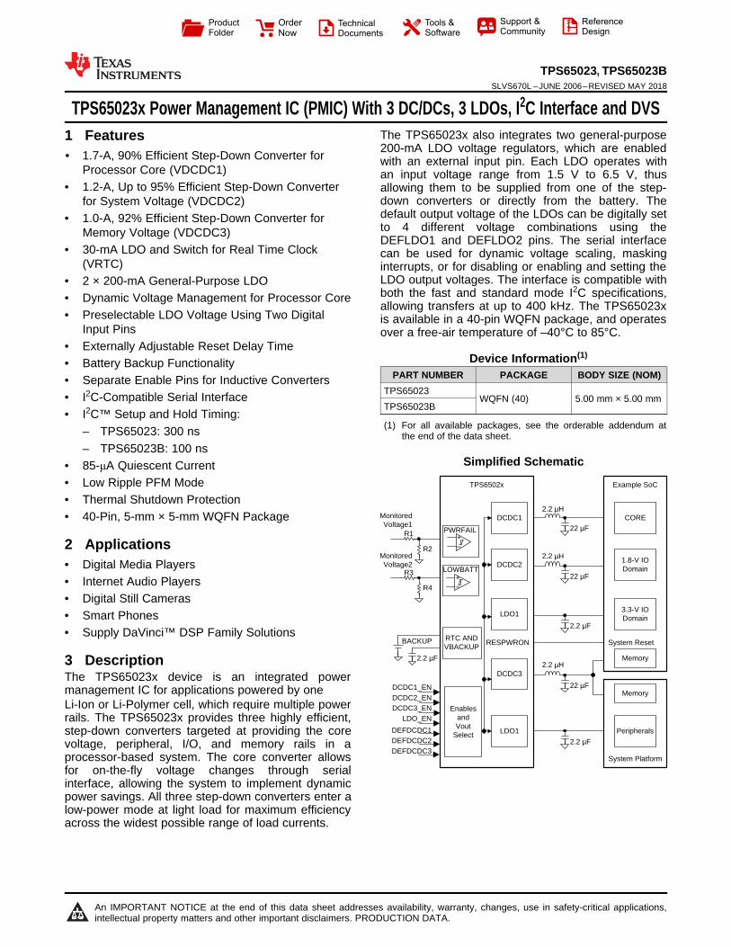
3 DescriptionThe TPS65023x device is an integrated powermanagement IC for applications powered by oneLi-Ion or Li-Polymer cell, which require multiple powerrails. The TPS65023x provides three highly efficient,step-down converters targeted at providing the corevoltage, peripheral, I/O, and memory rails in aprocessor-based system. The core converter allowsfor on-the-fly voltage changes through serialinterface, allowing the system to implement dynamicpower savings. All three step-down converters enter alow-power mode at light load for maximum efficiencyacross the widest possible range of load currents.
The TPS65023x also integrates two general-purpose200-mA LDO voltage regulators, which are enabledwith an external input pin. Each LDO operates withan input voltage range from 1.5 V to 6.5 V, thusallowing them to be supplied from one of the step-down converters or directly from the battery. Thedefault output voltage of the LDOs can be digitally setto 4 different voltage combinations using theDEFLDO1 and DEFLDO2 pins. The serial interfacecan be used for dynamic voltage scaling, maskinginterrupts, or for disabling or enabling and setting theLDO output voltages. The interface is compatible withboth the fast and standard mode I2C specifications,allowing transfers at up to 400 kHz. The TPS65023xis available in a 40-pin WQFN package, and operatesover a free-air temperature of –40°C to 85°C.
Device Information(1)
PART NUMBER PACKAGE BODY SIZE (NOM)TPS65023
WQFN (40) 5.00 mm × 5.00 mmTPS65023B
(1) For all available packages, see the orderable addendum atthe end of the data sheet.
Simplified Schematic
2
TPS65023, TPS65023BSLVS670L –JUNE 2006–REVISED MAY 2018 www.ti.com
Product Folder Links: TPS65023 TPS65023B
Submit Documentation Feedback Copyright © 2006–2018, Texas Instruments Incorporated
Table of Contents1 Features .................................................................. 12 Applications ........................................................... 13 Description ............................................................. 14 Revision History..................................................... 25 Pin Configuration and Functions ......................... 56 Specifications......................................................... 7
6.1 Absolute Maximum Ratings ...................................... 76.2 ESD Ratings.............................................................. 76.3 Recommended Operating Conditions....................... 76.4 Thermal Information .................................................. 86.5 Electrical Characteristics........................................... 86.6 Electrical Characteristics: Supply Pins VCC,
VINDCDC1, VINDCDC2, VINDCDC3...................... 106.7 Electrical Characteristics: Supply Pins VBACKUP,
VSYSIN, VRTC, VINLDO......................................... 106.8 Electrical Characteristics: VDCDC1 Step-Down
Converter ................................................................. 116.9 Electrical Characteristics: VDCDC2 Step-Down
Converter ................................................................. 126.10 Electrical Characteristics: VDCDC3 Step-Down
Converter ................................................................. 126.11 I2C Timing Requirements for TPS65023B ............ 136.12 Typical Characteristics .......................................... 16
7 Detailed Description ............................................ 21
7.1 Overview ................................................................. 217.2 Functional Block Diagram ....................................... 227.3 Feature Description................................................. 227.4 Device Functional Modes........................................ 277.5 Programming........................................................... 287.6 Register Maps ......................................................... 31
8 Application and Implementation ........................ 378.1 Application Information............................................ 378.2 Typical Application ................................................. 39
9 Power Supply Recommendations ...................... 449.1 Requirements for Supply Voltages Below 3.0 V..... 44
10 Layout................................................................... 4510.1 Layout Guidelines ................................................. 4510.2 Layout Example .................................................... 45
11 Device and Documentation Support ................. 4611.1 Device Support...................................................... 4611.2 Documentation Support ........................................ 4611.3 Related Links ........................................................ 4611.4 Community Resources.......................................... 4611.5 Trademarks ........................................................... 4711.6 Electrostatic Discharge Caution............................ 4711.7 Glossary ................................................................ 47
12 Mechanical, Packaging, and OrderableInformation ........................................................... 47
4 Revision HistoryNOTE: Page numbers for previous revisions may differ from page numbers in the current version.
Changes from Revision K (December 2015) to Revision L Page
• Changed the title of the data sheet ....................................................................................................................................... 1• Replaced references of TI PowerPAD IC package with thermal pad ................................................................................... 6• Added the Device Support and Documentation Support sections ....................................................................................... 46• Changed the Electrostatic Discharge Caution statement..................................................................................................... 46
Changes from Revision J (September 2011) to Revision K Page
• Added ESD Ratings table, Feature Description section, Device Functional Modes, Application and Implementationsection, Power Supply Recommendations section, Layout section, Device and Documentation Support section, andMechanical, Packaging, and Orderable Information section .................................................................................................. 1
Changes from Revision I (July 2010) to Revision J Page
• Added Thermal Information Table and deleted Dissipation Ratings Table ............................................................................ 8
Changes from Revision H (December 2009) to Revision I Page
• Added I2C Compatible Serial Interface to Features list .......................................................................................................... 1• Added TPS65023B device specs ........................................................................................................................................... 1• Added ordering info for TPS65023B device. ......................................................................................................................... 1• Added specs for TPS65023B device...................................................................................................................................... 8
3
TPS65023, TPS65023Bwww.ti.com SLVS670L –JUNE 2006–REVISED MAY 2018
Product Folder Links: TPS65023 TPS65023B
Submit Documentation FeedbackCopyright © 2006–2018, Texas Instruments Incorporated
• Changed "VBACKUP threshold" test condition typographical error from "VBACKUP falling" to "VBACKUP rising"........... 11• Added specs for TPS65023B device.................................................................................................................................... 13• Added Differences table for TPS65023 and TPS65023B devices ....................................................................................... 39
Changes from Revision G (October 2008) to Revision H Page
• Changed IO(DCDC1) MAX from: 1500 mA to: 1700 mA ............................................................................................................. 7• Added High level input voltage for the SDAT pin ................................................................................................................... 8• Changed IO from:1500 mA MIN to 1700 mA ....................................................................................................................... 11• Changed IO maximum from:1.5 A to: 1.7 A for VDCDC1 fixed and adjustable output voltage test condition specs. .......... 11• Changed IO maximum from: 1500 mA to: 1700 mA for VDCDC1 Load Regulation test condition ...................................... 11• Changed VDCDC1 "soft-start ramp time" spec to: "tStart and tRamp" specifications with MIN TYP MAX values. .................. 11• Changed VDCDC2 "soft-start ramp time" spec To: "tStart and tRamp" specifications with MIN TYP MAX values. ................. 12• Changed VDCDC3 "soft-start ramp time" spec To: "tStart and tRamp" specifications with MIN TYP MAX values. ................. 13• Changed FBD graphic to show 1700 mA for DCDC1 Buck Converter ................................................................................ 22• Changed text string from: "1.2 V or 1.8 V" to: "1.2 V to 1.6 V" in the STEP-DOWN CONVERTERS.,VDCDC1....
description. ........................................................................................................................................................................... 24• Changed graphic entity to the one used in the Application Note SLVA273......................................................................... 39
Changes from Revision F (July 2007) to Revision G Page
• Changed the Interrupt Management and the INT Pin section.............................................................................................. 28
Changes from Revision E (January 2007) to Revision F Page
• Changed text string from: "If it is tied to VCC, the default is 2.5 V" To: "If it is tied to VCC, the default is 3.3 V" ............... 24
Changes from Revision D (December 2006) to Revision E Page
• Changed LDO1 output voltage range from: 3.3 to: 3.3 .......................................................................................................... 9• Changed text string from: "VDCDC2 converter defaults to 1.8 V or 2.5 V" to: "VDCDC2 converter defaults to 1.8 V
or 3.3 V"................................................................................................................................................................................ 24
Changes from Revision C (October 2006) to Revision D Page
• Changed Typical Configuration for Ti DaVinci Processors .................................................................................................. 39
Changes from Revision B (June 2006) to Revision C Page
• Changed from: AD Coupled to: AD Coupled - Figure 16 .................................................................................................... 17• Changed from: AD Coupled to: AD Coupled - Figure 17 .................................................................................................... 18
Changes from Revision A (June 2006) to Revision B Page
• Changed from: 1.5A and 97% Efficient Step-Down to: 1.7A and 90% Efficient Step-Down.................................................. 1• Changed from: 6 mm × 6 mm QFN Package to: 5 mm × 5 mm QFN Package .................................................................... 1• Changed from: RHA package to: RSB package .................................................................................................................... 1• Changed from:O(DCDC2) to: IO(DCDC1) ........................................................................................................................................ 7• Changed Forward current limit - removed TBD and added values ...................................................................................... 11
4
TPS65023, TPS65023BSLVS670L –JUNE 2006–REVISED MAY 2018 www.ti.com
Product Folder Links: TPS65023 TPS65023B
Submit Documentation Feedback Copyright © 2006–2018, Texas Instruments Incorporated
• Changed Fixed output voltage - removed TBD and added values ...................................................................................... 11• Changed Fixed output voltage - removed TBD and added values ...................................................................................... 12• Added VINDCDC3 = 3.6 V to Maximum output current ....................................................................................................... 12• Changed Fixed output voltage - removed TBD and added values ...................................................................................... 13• Changed Figure 3 (DVS Timing) .......................................................................................................................................... 15• Changed Figure 11 (Graph - DCDC2: OUTPUT VOLTAGE)............................................................................................... 17• Added Figure 12 (Graph - DCDC3: OUTPUT VOLTAGE ).................................................................................................. 17• Changed Figure 20 (Graph - VDCDC2 OUTPUT VOLTAGE RIPPLE) ............................................................................... 18• Added Reset Condition of DCDC1 Information .................................................................................................................... 37• Changed Typical Configuration for Ti DaVinci Processors .................................................................................................. 39• Changed from: TPS65023 typically use a 3.3 μH output inductor to: TPS65023 typically use a 2.2 μH output inductor.... 40• Changed from: VDCDC3 to: VDCDC1 ................................................................................................................................. 41• Changed from: VDEFDCDC3 to: DEFDCDC1 ..................................................................................................................... 41• Changed from: 2.5 V to 3.3 V (Table 20) ............................................................................................................................. 41
Changes from Original (May 2006) to Revision A Page
• Changed Electrical Characteristics: VDCDC1 Step-Down Converter .................................................................................. 11• Changed Electrical Characteristics: VDCDC3 Step-Down Converter ................................................................................. 12• Changed CON_CTRL Register Address - Column B0 default value changed from 1 to 0.................................................. 33• Changed VDCDC# to VDCDC1 ........................................................................................................................................... 35
1
2
3
4
5
6
7
8
9
10
30
29
28
27
26
25
24
23
22
21
11 12 13 14 15 16 17 18 19 20
40 39 38 37 36 35 34 33 32 31
DEFDCDC3
VDCDC3
PGND3
L3
VINDCDC3
VINDCDC1
L1
PGND1
VDCDC1
DEFDCDC1
HO
T_
RE
SE
T
DE
FL
DO
1
DE
FL
DO
2
VS
YS
IN
VB
AC
KU
P
VR
TC
AG
ND
2
VIN
LD
O
VL
DO
1
VL
DO
2
SCLK
SDAT
INT
RESPWRON
TRESPWRON
DCDC1_EN
DCDC2_EN
DCDC3_EN
LDO_EN
LOWBAT
AG
ND
1
LO
WB
AT
_S
NS
PW
RFA
IL_
SN
S
VC
C
VIN
DC
DC
2
L2
PG
ND
2
VD
CD
C2
DE
FD
CD
C2
PW
RFA
IL
5
TPS65023, TPS65023Bwww.ti.com SLVS670L –JUNE 2006–REVISED MAY 2018
Product Folder Links: TPS65023 TPS65023B
Submit Documentation FeedbackCopyright © 2006–2018, Texas Instruments Incorporated
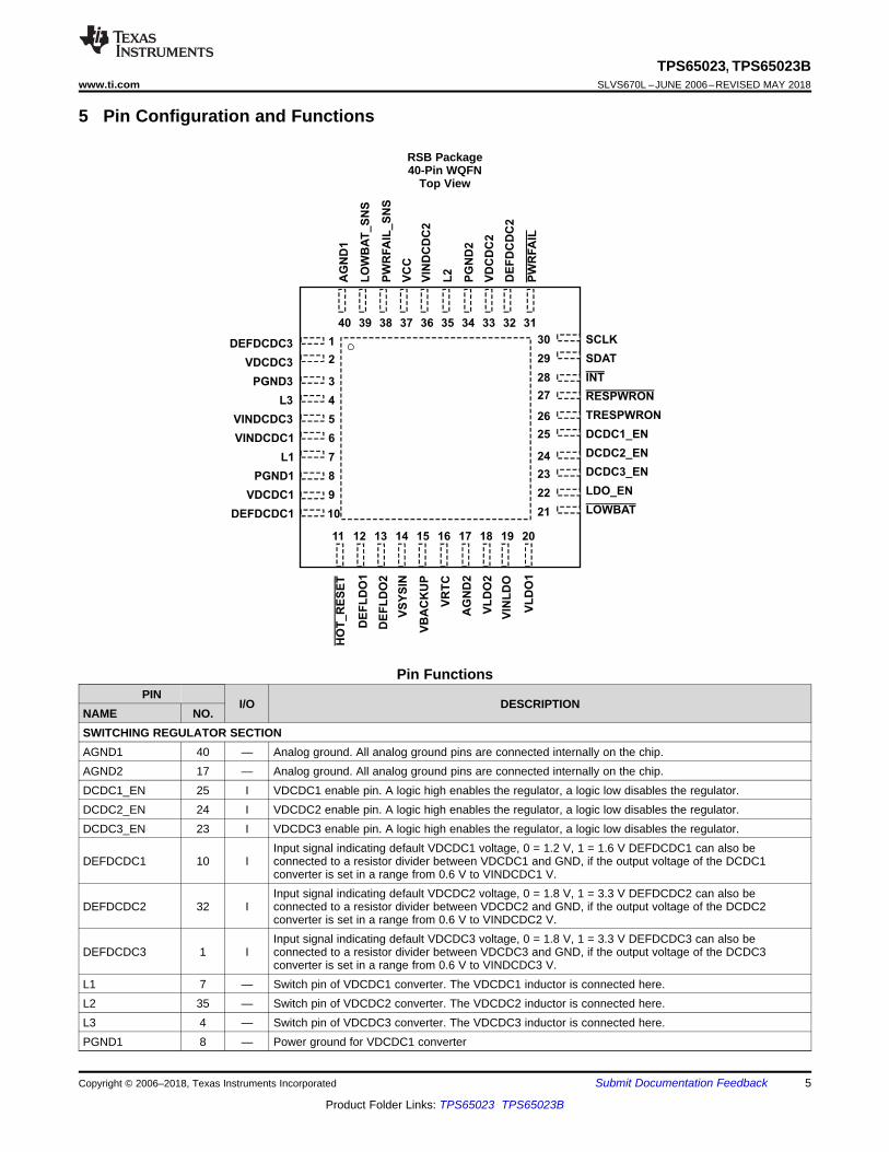
5 Pin Configuration and Functions
RSB Package40-Pin WQFN
Top View
Pin FunctionsPIN
I/O DESCRIPTIONNAME NO.SWITCHING REGULATOR SECTIONAGND1 40 — Analog ground. All analog ground pins are connected internally on the chip.AGND2 17 — Analog ground. All analog ground pins are connected internally on the chip.DCDC1_EN 25 I VDCDC1 enable pin. A logic high enables the regulator, a logic low disables the regulator.DCDC2_EN 24 I VDCDC2 enable pin. A logic high enables the regulator, a logic low disables the regulator.DCDC3_EN 23 I VDCDC3 enable pin. A logic high enables the regulator, a logic low disables the regulator.
DEFDCDC1 10 IInput signal indicating default VDCDC1 voltage, 0 = 1.2 V, 1 = 1.6 V DEFDCDC1 can also beconnected to a resistor divider between VDCDC1 and GND, if the output voltage of the DCDC1converter is set in a range from 0.6 V to VINDCDC1 V.
DEFDCDC2 32 IInput signal indicating default VDCDC2 voltage, 0 = 1.8 V, 1 = 3.3 V DEFDCDC2 can also beconnected to a resistor divider between VDCDC2 and GND, if the output voltage of the DCDC2converter is set in a range from 0.6 V to VINDCDC2 V.
DEFDCDC3 1 IInput signal indicating default VDCDC3 voltage, 0 = 1.8 V, 1 = 3.3 V DEFDCDC3 can also beconnected to a resistor divider between VDCDC3 and GND, if the output voltage of the DCDC3converter is set in a range from 0.6 V to VINDCDC3 V.
L1 7 — Switch pin of VDCDC1 converter. The VDCDC1 inductor is connected here.L2 35 — Switch pin of VDCDC2 converter. The VDCDC2 inductor is connected here.L3 4 — Switch pin of VDCDC3 converter. The VDCDC3 inductor is connected here.PGND1 8 — Power ground for VDCDC1 converter

6
TPS65023, TPS65023BSLVS670L –JUNE 2006–REVISED MAY 2018 www.ti.com
Product Folder Links: TPS65023 TPS65023B
Submit Documentation Feedback Copyright © 2006–2018, Texas Instruments Incorporated
Pin Functions (continued)PIN
I/O DESCRIPTIONNAME NO.PGND2 34 — Power ground for VDCDC2 converterPGND3 3 — Power ground for VDCDC3 converter
VCC 37 IPower supply for digital and analog circuitry of VDCDC1, VDCDC2, and VDCDC3 DC-DC converters.VCC must be connected to the same voltage supply as VINDCDC3, VINDCDC1, and VINDCDC2.VCC also supplies serial interface block.
VDCDC1 9 I VDCDC1 feedback voltage sense input. Connect directly to VDCDC1VDCDC2 33 I VDCDC2 feedback voltage sense input. Connect directly to VDCDC2VDCDC3 2 I VDCDC3 feedback voltage sense input. Connect directly to VDCDC3
VINDCDC1 6 I Input voltage for VDCDC1 step-down converter. VINDCDC1 must be connected to the same voltagesupply as VINDCDC2, VINDCDC3, and VCC.
VINDCDC2 36 I Input voltage for VDCDC2 step-down converter. VINDCDC2 must be connected to the same voltagesupply as VINDCDC1, VINDCDC3, and VCC.
VINDCDC3 5 I Input voltage for VDCDC3 step-down converter. VINDCDC3 must be connected to the same voltagesupply as VINDCDC1, VINDCDC2, and VCC.
Thermal Pad — — Connect the power pad to analog groundLDO REGULATOR SECTIONDEFLD01 12 I Digital input. DEFLD01 sets the default output voltage of LDO1 and LDO2.DEFLD02 13 I Digital input. DEFLD02 sets the default output voltage of LDO1 and LDO2.LDO_EN 22 I Enable input for LDO1 and LDO2. A logic high enables the LDOs and a logic low disables the LDOs.VBACKUP 15 I Connect the backup battery to this input pinVINLDO 19 I Input voltage for LDO1 and LDO2VLDO1 20 O Output voltage of LDO1VLDO2 18 O Output voltage of LDO2VRTC 16 O Output voltage of the LDO and switch for the real time clockVSYSIN 14 I Input of system voltage for VRTC switchCONTROL AND I2C SECTIONHOT_RESET 11 I Push button input that reboots or wakes up the processor through the RESPWRON output pin.INT 28 O Open-drain outputLOW_BAT 21 O Open-drain output of LOW_BAT comparatorLOWBAT_SNS 39 I Input for the comparator driving the LOW_BAT output.PWRFAIL 31 O Open-drain output. Active low when PWRFAIL comparator indicates low VBAT condition.PWRFAIL_SNS 38 I Input for the comparator driving the PWRFAIL outputRESPWRON 27 O Open-drain system reset outputSCLK 30 I Serial interface clock lineSDAT 29 I/O Serial interface data and addressTRESPWRON 26 I Connect the timing capacitor to TRESPWRON to set the reset delay time: 1 nF → 100 ms

7
TPS65023, TPS65023Bwww.ti.com SLVS670L –JUNE 2006–REVISED MAY 2018
Product Folder Links: TPS65023 TPS65023B
Submit Documentation FeedbackCopyright © 2006–2018, Texas Instruments Incorporated
(1) Stresses beyond those listed under Absolute Maximum Ratings may cause permanent damage to the device. These are stress ratingsonly, which do not imply functional operation of the device at these or any other conditions beyond those indicated under RecommendedOperating Conditions. Exposure to absolute-maximum-rated conditions for extended periods may affect device reliability.
6 Specifications
6.1 Absolute Maximum Ratingsover operating free-air temperature range (unless otherwise noted) (1)
MIN MAX UNITVI Input voltage on all pins except AGND and PGND pins with respect to AGND –0.3 7 V
Current at VINDCDC1, L1, PGND1, VINDCDC2, L2, PGND2, VINDCDC3, L3,PGND3 2000 mA
Peak current at all other pins 1000 mAContinuous total power dissipation See Thermal Information
TA Operating free-air temperature –40 85 °CTJ Maximum junction temperature 125 °CTstg Storage temperature –65 150 °C
(1) JEDEC document JEP155 states that 500-V HBM allows safe manufacturing with a standard ESD control process.(2) JEDEC document JEP157 states that 250-V CDM allows safe manufacturing with a standard ESD control process.
6.2 ESD RatingsVALUE UNIT
V(ESD) Electrostatic dischargeHuman-body model (HBM), per ANSI/ESDA/JEDEC JS-001 (1) ±2000
VCharged-device model (CDM), per JEDEC specification JESD22-C101 (2) ±500
(1) When using an external resistor divider at DEFDCDC3, DEFDCDC2, and DEFDCDC1(2) See Application Information section for more information.
6.3 Recommended Operating Conditionsover operating free-air temperature range (unless otherwise noted)
MIN NOM MAX UNIT
VCC
Input voltage step-down converters(VINDCDC1, VINDCDC2, VINDCDC3); pins need to be tied to the samevoltage rail
2.5 6 V
VO
Output voltage for VDCDC1 step-down converter (1) 0.6 VINDCDC1VOutput voltage for VDCDC2 step-down converter (1) 0.6 VINDCDC2
Output voltage for VDCDC3 step-down converter (1) 0.6 VINDCDC3VI Input voltage for LDOs (VINLDO1, VINLDO2) 1.5 6.5 VVO Output voltage for LDOs (VLDO1, VLDO2) 1 VINLDO1–2 VIO(DCDC1) Output current at L1 1700 mA
Inductor at L1 (2) 1.5 2.2 μHCI(DCDC1) Input capacitor at VINDCDC1 (2) 10 μFCO(DCDC1) Output capacitor at VDCDC1 (2) 10 22 μFIO(DCDC2) Output current at L2 1200 mA
Inductor at L2 (2) 1.5 2.2 μHCI(DCDC2) Input capacitor at VINDCDC2 (2) 10 μFCO(DCDC2) Output capacitor at VDCDC2 (2) 10 22 μFIO(DCDC3) Output current at L3 1000 mA
Inductor at L3 (2) 1.5 2.2 μHCI(DCDC3) Input capacitor at VINDCDC3 (2) 10 μFCO(DCDC3) Output capacitor at VDCDC3 (2) 10 22 μFCI(VCC) Input capacitor at VCC (2) 1 μFCi(VINLDO) Input capacitor at VINLDO (2) 1 μFCO(VLDO1-2) Output capacitor at VLDO1, VLDO2 (2) 2.2 μF

8
TPS65023, TPS65023BSLVS670L –JUNE 2006–REVISED MAY 2018 www.ti.com
Product Folder Links: TPS65023 TPS65023B
Submit Documentation Feedback Copyright © 2006–2018, Texas Instruments Incorporated
Recommended Operating Conditions (continued)over operating free-air temperature range (unless otherwise noted)
MIN NOM MAX UNIT
(3) Up to 3 mA can flow into VCC when all 3 converters are running in PWM. This resistor causes the UVLO threshold to be shiftedaccordingly.
IO(VLDO1-2) Output current at VLDO1, VLDO2 200 mACO(VRTC) Output capacitor at VRTC (2) 4.7 μFTA Operating ambient temperature –40 85 °CTJ Operating junction temperature –40 125 °C
Resistor from VINDCDC3, VINDCDC2, VINDCDC1 to VCC used for filtering (3) 1 10 Ω
(1) For more information about traditional and new thermal metrics, see the Semiconductor and IC Package Thermal Metrics applicationreport.
6.4 Thermal Information
THERMAL METRIC (1)TPS65023x
UNITRSB (WQFN)40 PINS
RθJA Junction-to-ambient thermal resistance 32.7 °C/WRθJC(top) Junction-to-case (top) thermal resistance 15.3 °C/WRθJB Junction-to-board thermal resistance 13.6 °C/WψJT Junction-to-top characterization parameter 0.1 °C/WψJB Junction-to-board characterization parameter 5.4 °C/WRθJC(bot) Junction-to-case (bottom) thermal resistance 1.1 °C/W
(1) Typical values are at TA = 25°C, unless otherwise noted.
6.5 Electrical CharacteristicsVINDCDC1 = VINDCDC2 = VINDCDC3 = VCC = VINLDO = 3.6 V, VBACKUP = 3 V, TA = –40°C to 85°C (unless otherwisenoted)
PARAMETER TEST CONDITIONS MIN TYP (1) MAX UNIT
CONTROL SIGNALS: SCLK, SDAT (INPUT) FOR TPS65023
VIHHigh level input voltage (except theSDAT pin)
Resistor pullup at SCLK = 4.7 kΩ, pulled toVRTC 1.3 VCC V
VIH High level input voltage for the SDAT pin Resistor pullup at SDAT = 4.7 kΩ, pulled toVRTC 1.45 VCC V
VIL Low level input voltage Resistor pullup at SCLK and SDAT = 4.7 kΩ,pulled to VRTC 0 0.4 V
IH Input bias current 0.01 0.1 μA
CONTROL SIGNALS: SCLK, SDAT (INPUT) FOR TPS65023B
VIH High level input voltage for the SCLK pin Rpullup at SCLK = 4.7 kΩ, pulled to VRTC;For VCC = 2.5 V to 5.25 V 1.4 VCC V
VIH High level input voltage for the SDAT pin Rpullup at SDAT = 4.7 kΩ, pulled to VRTC;For VCC = 2.5 V to 5.25 V 1.69 VCC V
VIH High level input voltage for the SDAT pin Rpullup at SDAT = 4.7 kΩ, pulled to VRTC;For VCC = 2.5 V to 4.5 V 1.55 VCC V
VIL Low level input voltage Rpullup at SCLK and SDAT = 4.7 kΩ, pulled toVRTC 0 0.35 V
IH Input bias current 0.01 0.1 μA
CONTROL SIGNALS: HOT_RESET, DCDC1_EN, DCDC2_EN, DCDC3_EN, LDO_EN, DEFLDO1, DEFLDO2
VIH High-level input voltage 1.3 VCC V
VIL Low-level input voltage 0 0.4 V
IIB Input bias current 0.01 0.1 μA
tdeglitch Deglitch time at HOT_RESET 25 30 35 ms

9
TPS65023, TPS65023Bwww.ti.com SLVS670L –JUNE 2006–REVISED MAY 2018
Product Folder Links: TPS65023 TPS65023B
Submit Documentation FeedbackCopyright © 2006–2018, Texas Instruments Incorporated
Electrical Characteristics (continued)VINDCDC1 = VINDCDC2 = VINDCDC3 = VCC = VINLDO = 3.6 V, VBACKUP = 3 V, TA = –40°C to 85°C (unless otherwisenoted)
PARAMETER TEST CONDITIONS MIN TYP (1) MAX UNIT
CONTROL SIGNALS: LOWBAT, PWRFAIL, RESPWRON, INT, SDAT (OUTPUT)
VOH High-level output voltage 6 V
VOL Low-level output voltage IIL = 5 mA 0 0.3 V
Duration of low pulse at RESPWRON External capacitor 1 nF 100 ms
ICONST Internal charge / discharge current on pinTRESPWRON Used for generating RESPWRON delay 1.7 2 2.3 μA
TRESPWRON_LOWTH Internal lower comparator threshold onpin TRESPWRON Used for generating RESPWRON delay 0.225 0.25 0.275 V
TRESPWRON_UPTH Internal upper comparator threshold onpin TRESPWRON Used for generating RESPWRON delay 0.97 1 1.103 V
Resetpwron threshold VRTC falling –3% 2.4 3% V
Resetpwron threshold VRTC rising –3% 2.52 3% V
ILK Leakage current Output inactive high 0.1 μA
VLDO1 AND VLDO2 LOW DROPOUT REGULATORS
VI Input voltage range for LDO1, 2 1.5 6.5 V
VO(LD01) LDO1 output voltage range 1 3.15 V
VO(LDO2) LDO2 output voltage range 1 3.3 V
IOMaximum output current for LDO1,LDO2
VI = 1.8 V, VO = 1.3 V 200mA
VI = 1.5 V, VO = 1.3 V 120
I(SC)LDO1 and LDO2 short-circuit currentlimit V(LDO1) = GND, V(LDO2) = GND 400 mA
Minimum voltage drop at LDO1, LDO2
IO = 50 mA, VINLDO = 1.8 V 120
mVIO = 50 mA, VINLDO = 1.5 V 65 150
IO = 200 mA, VINLDO = 1.8 V 300
Output voltage accuracy for LDO1,LDO2 IO = 10 mA –2% 1%
Line regulation for LDO1, LDO2 VINLDO1, 2 = VLDO1,2 + 0.5 V(min. 2.5 V) to 6.5 V, IO = 10 mA –1% 1%
Load regulation for LDO1, LDO2 IO = 0 mA to 50 mA –1% 1%
Regulation time for LDO1, LDO2 Load change from 10% to 90% 10 μs
ANALOGIC SIGNALS DEFDCDC1, DEFDCDC2, DEFDCDC3
VIH High-level input voltage 1.3 VCC V
VIL Low-level input voltage 0 0.1 V
Input bias current 0.001 0.05 μA
THERMAL SHUTDOWN
T(SD) Thermal shutdown Increasing junction temperature 160 °C
Thermal shutdown hysteresis Decreasing junction temperature 20 °C
INTERNAL UNDERVOLTAGE LOCK OUT
UVLO Internal UVLO VCC falling –2% 2.35 2% V
V(UVLO_HYST) Internal UVLO comparator hysteresis 120 mV
VOLTAGE DETECTOR COMPARATORS
Comparator threshold(PWRFAIL_SNS, LOWBAT_SNS) Falling threshold –1% 1 1% V
Hysteresis 40 50 60 mV
Propagation delay 25-mV overdrive 10 μs
POWER-GOOD
V(PGOODF)VDCDC1, VDCDC2, VDCDC3, VLDO1,VLDO2, decreasing –12% –10% –8%
V(PGOODR)VDCDC1, VDCDC2, VDCDC3, VLDO1,VLDO2, increasing –7% –5% –3%
10
TPS65023, TPS65023BSLVS670L –JUNE 2006–REVISED MAY 2018 www.ti.com
Product Folder Links: TPS65023 TPS65023B
Submit Documentation Feedback Copyright © 2006–2018, Texas Instruments Incorporated
(1) Typical values are at TA = 25°C, unless otherwise noted.
6.6 Electrical Characteristics: Supply Pins VCC, VINDCDC1, VINDCDC2, VINDCDC3VINDCDC1 = VINDCDC2 = VINDCDC3 = VCC = VINLDO = 3.6 V, VBACKUP = 3 V, TA = –40°C to 85°C (unless otherwisenoted)
PARAMETER TEST CONDITIONS MIN TYP (1) MAX UNIT
I(q)Operating quiescentcurrent, PFM
All 3 DCDC converters enabled, zeroload, and no switching, LDOs enabled
VCC = 3.6 V, VBACKUP = 3 V;V(VSYSIN) = 0 V 85 100
μA
All 3 DCDC converters enabled, zeroload, and no switching, LDOs off
VCC = 3.6 V, VBACKUP = 3 V;V(VSYSIN) = 0 V 78 90
DCDC1 and DCDC2 convertersenabled, zero load, and no switching,LDOs off
VCC = 3.6 V, VBACKUP = 3 V;V(VSYSIN) = 0 V 57 70
DCDC1 converter enabled, zero load,and no switching, LDOs off
VCC = 3.6 V, VBACKUP = 3 V;V(VSYSIN) = 0 V 43 55
II Current into VCC; PWM
All 3 DCDC converters enabled andrunning in PWM, LDOs off
VCC = 3.6 V, VBACKUP = 3 V;V(VSYSIN) = 0 V 2 3
mADCDC1 and DCDC2 convertersenabled and running in PWM, LDOsoff
VCC = 3.6 V, VBACKUP = 3 V;V(VSYSIN) = 0 V 1.5 2.5
DCDC1 converter enabled and runningin PWM, LDOs off
VCC = 3.6 V, VBACKUP = 3 V;V(VSYSIN) = 0 V 0.85 2
I(q) Quiescent current All converters disabled, LDOs off
VCC = 3.6 V, VBACKUP = 3 V;V(VSYSIN) = 0 V 23 33 μA
VCC = 2.6 V, VBACKUP = 3 V;V(VSYSIN) = 0 V 3.5 5 μA
VCC = 3.6 V, VBACKUP = 0 V;V(VSYSIN) = 0 V 43 μA
(1) Typical values are at TA = 25°C, unless otherwise noted.(2) Based on the requirements for the Intel PXA270 processor.
6.7 Electrical Characteristics: Supply Pins VBACKUP, VSYSIN, VRTC, VINLDOVINDCDC1 = VINDCDC2 = VINDCDC3 = VCC = VINLDO = 3.6 V, VBACKUP = 3 V, TA = –40°C to 85°C (unless otherwisenoted)
PARAMETER TEST CONDITIONS MIN TYP (1) MAX UNITVBACKUP, VSYSIN, VRTC
I(q) Operating quiescent current VBACKUP = 3 V, VSYSIN = 0 V;VCC = 2.6 V, current into VBACKUP 20 33 μA
I(SD) Operating quiescent current VBACKUP < V_VBACKUP, current intoVBACKUP 2 3 μA
VRTC LDO output voltage VSYSIN = VBACKUP = 0 V, IO = 0 mA 3 VIO Output current for VRTC VSYSIN < 2.57 V and VBACKUP < 2.57 V 30 mA
VRTC short-circuit current limit VRTC = GND; VSYSIN = VBACKUP = 0 V 100 mAMaximum output current at VRTC forRESPWRON = 1
VRTC > 2.6 V, VCC = 3 V;VSYSIN = VBACKUP = 0 V 30 mA
VO Output voltage accuracy for VRTC VSYSIN = VBACKUP = 0 V; IO = 0 mA –1% 1%Line regulation for VRTC VCC = VRTC + 0.5 V to 6.5 V, IO = 5 mA –1% 1%
Load regulation VRTC IO = 1 mA to 30 mA;VSYSIN = VBACKUP = 0 V –3% 1%
Regulation time for VRTC Load change from 10% to 90% 10 μsIlkg Input leakage current at VSYSIN VSYSIN < V_VSYSIN 2 μA
rDS(on) of VSYSIN switch 12.5 ΩrDS(on) of VBACKUP switch 12.5 ΩInput voltage range at VBACKUP (2) 2.73 3.75 VInput voltage range at VSYSIN (2) 2.73 3.75 VVSYSIN threshold VSYSIN falling –3% 2.55 3% V
11
TPS65023, TPS65023Bwww.ti.com SLVS670L –JUNE 2006–REVISED MAY 2018
Product Folder Links: TPS65023 TPS65023B
Submit Documentation FeedbackCopyright © 2006–2018, Texas Instruments Incorporated
Electrical Characteristics: Supply Pins VBACKUP, VSYSIN, VRTC, VINLDO (continued)VINDCDC1 = VINDCDC2 = VINDCDC3 = VCC = VINLDO = 3.6 V, VBACKUP = 3 V, TA = –40°C to 85°C (unless otherwisenoted)
PARAMETER TEST CONDITIONS MIN TYP (1) MAX UNITVSYSIN threshold VSYSIN rising –3% 2.65 3% VVBACKUP threshold VBACKUP falling –3% 2.55 3% VVBACKUP threshold VBACKUP rising –3% 2.65 3% V
VINLDO
I(q) Operating quiescent current Current per LDO into VINLDOfor LDO_CTRL = 0x0 16 30 μA
I(SD) Shutdown current Total current for both LDOs into VINLDO,VLDO = 0 V 0.1 1 μA
(1) Typical values are at TA = 25°C, unless otherwise noted.
6.8 Electrical Characteristics: VDCDC1 Step-Down ConverterVINDCDC1 = VINDCDC2 = VINDCDC3 = VCC = VINLDO = 3.6 V, VBACKUP = 3 V, TA = –40°C to 85°C (unless otherwisenoted)
PARAMETER TEST CONDITIONS MIN TYP (1) MAX UNITVI Input voltage range, VINDCDC1 2.5 6 VIO Maximum output current 1700 mAI(SD) Shutdown supply current in VINDCDC1 DCDC1_EN = GND 0.1 1 μArDS(on) P-channel MOSFET on-resistance VINDCDC1 = V(GS) = 3.6 V 125 261 mΩIlkg P-channel leakage current VINDCDC1 = 6 V 2 μArDS(on) N-channel MOSFET on-resistance VINDCDC1 = V(GS) = 3.6 V 130 260 mΩIlkg N-channel leakage current V(DS) = 6 V 7 10 μA
Forward current limit (P-channel andN-channel) 2.5 V < VI(MAIN) < 6 V 1.94 2.19 2.44 A
fS Oscillator frequency 1.95 2.25 2.55 MHzFixed output voltageFPWMDCDC1 = 0
All VDCDC1
VINDCDC1 = 2.5 V to 6 V;0 mA ≤ IO ≤ 1.7 A –2% 2%
Fixed output voltageFPWMDCDC1 = 1
VINDCDC1 = 2.5 V to 6 V;0 mA ≤ IO ≤ 1.7 A –1% 1%
Adjustable output voltage with resistor dividerat DEFDCDC1; FPWMDCDC1 = 0
VINDCDC1 = VDCDC1 + 0.5 V (min 2.5 V)to 6 V; 0 mA ≤ IO ≤ 1.7 A –2% 2%
Adjustable output voltage with resistor dividerat DEFDCDC1; FPWMDCDC1 = 1
VINDCDC1 = VDCDC1 + 0.5 V (min 2.5 V)to 6 V; 0 mA ≤ IO ≤ 1.7 A –1% 1%
Line Regulation VINDCDC1 = VDCDC1 + 0.3 V (min. 2.5 V)to 6 V; IO = 10 mA 0% V
Load Regulation IO = 10 mA to 1700 mA 0.25% AtStart Start-up time Time from active EN to start switching 145 175 200 μstRamp VOUT ramp-up time Time to ramp from 5% to 95% of VOUT 400 750 1000 μs
Internal resistance from L1 to GND 1 MΩVDCDC1 discharge resistance DCDC1 discharge = 1 300 Ω

12
TPS65023, TPS65023BSLVS670L –JUNE 2006–REVISED MAY 2018 www.ti.com
Product Folder Links: TPS65023 TPS65023B
Submit Documentation Feedback Copyright © 2006–2018, Texas Instruments Incorporated
(1) Typical values are at TA = 25°C, unless otherwise noted.
6.9 Electrical Characteristics: VDCDC2 Step-Down ConverterVINDCDC1 = VINDCDC2 = VINDCDC3 = VCC = VINLDO = 3.6 V, VBACKUP = 3 V, TA = –40°C to 85°C (unless otherwisenoted)
PARAMETER TEST CONDITIONS MIN TYP (1) MAX UNITVI Input voltage range, VINDCDC2 2.5 6 V
IO Maximum output currentDEFDCDC2 = GND 1200
mAVINDCDC2 = 3.6 V;3.3 V - 1% ≤ VDCDC2 ≤ 3.3V + 1% 1000
I(SD) Shutdown supply current in VINDCDC2 DCDC2_EN = GND 0.1 1 μArDS(on) P-channel MOSFET on-resistance VINDCDC2 = V(GS) = 3.6 V 140 300 mΩIlkg P-channel leakage current VINDCDC2 = 6 V 2 μArDS(on) N-channel MOSFET on-resistance VINDCDC2 = V(GS) = 3.6 V 150 297 mΩIlkg N-channel leakage current V(DS) = 6 V 7 10 μA
ILIMFForward current limit (P-channel and N-channel) 2.5 V < VINDCDC2 < 6 V 1.74 1.94 2.12 A
fS Oscillator frequency 1.95 2.25 2.55 MHz
Fixed output voltageFPWMDCDC2=0
VDCDC2 = 1.8 V VINDCDC2 = 2.5 V to 6 V;0 mA ≤ IO ≤ 1.2 A –2% 2%
VDCDC2 = 3.3 V VINDCDC2 = 3.7 V to 6 V;0 mA ≤ IO ≤ 1.2 A –1% 1%
Fixed output voltageFPWMDCDC2=1
VDCDC2 = 1.8 V VINDCDC2 = 2.5 V to 6 V;0 mA ≤ IO ≤ 1.2 A –2% 2%
VDCDC2 = 3.3 V VINDCDC2 = 3.7 V to 6 V;0 mA ≤ IO ≤ 1.2 A –1% 1%
Adjustable output voltage with resistordivider at DEFDCDC2 FPWMDCDC2=0
VINDCDC2 = VDCDC2 + 0.3 V (min 2.5 V) to 6V; 0 mA ≤ IO ≤ 1 A –2% 2%
Adjustable output voltage with resistordivider at DEFDCDC2; FPWMDCDC2=1
VINDCDC2 = VDCDC2 + 0.3 V (min 2.5 V) to 6V; 0 mA ≤ IO ≤ 1 A –1% 1%
Line Regulation VINDCDC2 = VDCDC2 + 0.3 V (min. 2.5 V) to 6V; IO = 10 mA 0% V
Load Regulation IO = 10 mA to 1000 mA 0.25% AtStart Start-up time Time from active EN to start switching 145 175 200 µstRamp VOUT ramp-up time Time to ramp from 5% to 95% of VOUT 400 750 1000 μs
Internal resistance from L2 to GND 1 MΩVDCDC2 discharge resistance DCDC2 discharge =1 300 Ω
(1) Typical values are at TA = 25°C, unless otherwise noted.
6.10 Electrical Characteristics: VDCDC3 Step-Down ConverterVINDCDC1 = VINDCDC2 = VINDCDC3 = VCC = VINLDO = 3.6 V, VBACKUP = 3 V, TA = –40°C to 85°C (unless otherwisenoted)
PARAMETER TEST CONDITIONS MIN TYP (1) MAX UNITVI Input voltage range, VINDCDC3 2.5 6 V
IO Maximum output currentDEFDCDC3 = GND 1000
mAVINDCDC3 = 3.6 V;3.3V - 1% ≤ VDCDC3 ≤ 3.3V + 1% 525
I(SD) Shutdown supply current in VINDCDC3 DCDC3_EN = GND 0.1 1 μArDS(on) P-channel MOSFET on-resistance VINDCDC3 = V(GS) = 3.6 V 310 698 mΩIlkg P-channel leakage current VINDCDC3 = 6 V 0.1 2 μArDS(on) N-channel MOSFET on-resistance VINDCDC3 = V(GS) = 3.6 V 220 503 mΩIlkg N-channel leakage current V(DS) = 6 V 7 10 μA
Forward current limit (P-channel and N-channel) 2.5 V < VINDCDC3 < 6 V 1.28 1.49 1.69 A
13
TPS65023, TPS65023Bwww.ti.com SLVS670L –JUNE 2006–REVISED MAY 2018
Product Folder Links: TPS65023 TPS65023B
Submit Documentation FeedbackCopyright © 2006–2018, Texas Instruments Incorporated
Electrical Characteristics: VDCDC3 Step-Down Converter (continued)VINDCDC1 = VINDCDC2 = VINDCDC3 = VCC = VINLDO = 3.6 V, VBACKUP = 3 V, TA = –40°C to 85°C (unless otherwisenoted)
PARAMETER TEST CONDITIONS MIN TYP (1) MAX UNITfS Oscillator frequency 1.95 2.25 2.55 MHz
Fixed output voltageFPWMDCDC3=0
VDCDC3 = 1.8 V VINDCDC3 = 2.5 V to 6 V;0 mA ≤ IO ≤ 1 A –2% 2%
VDCDC3 = 3.3 V VINDCDC3 = 3.6 V to 6 V;0 mA ≤ IO ≤ 1 A –1% 1%
Fixed output voltageFPWMDCDC3=1
VDCDC3 = 1.8 V VINDCDC3 = 2.5 V to 6 V;0 mA ≤ IO ≤ 1 A –2% 2%
VDCDC3 = 3.3 V VINDCDC3 = 3.6 V to 6 V;0 mA ≤ IO ≤ 1 A –1% 1%
Adjustable output voltage with resistordivider at DEFDCDC3 FPWMDCDC3=0
VINDCDC3 = VDCDC3 + 0.5 V (min 2.5 V) to6 V; 0 mA ≤ IO ≤ 800 mA –2% 2%
Adjustable output voltage with resistordivider at DEFDCDC3; FPWMDCDC3=1
VINDCDC3 = VDCDC3 + 0.5 V (min 2.5 V) to6 V; 0 mA ≤ IO ≤ 800 mA –1% 1%
Line Regulation VINDCDC3 = VDCDC3 + 0.3 V (min. 2.5 V) to6 V; IO = 10 mA 0% V
Load Regulation IO = 10 mA to 1000 mA 0.25% AtStart Start-up time Time from active EN to start switching 145 175 200 µstRamp VOUT ramp-up time Time to ramp from 5% to 95% of VOUT 400 750 1000 μs
Internal resistance from L3 to GND 1 MΩVDCDC3 discharge resistance DCDC3 discharge =1 300 Ω
6.11 I2C Timing Requirements for TPS65023BVINDCDC1 = VINDCDC2 = VINDCDC3 = VCC = VINLDO = 2.5 V to 5.5 V, VBACKUP = 3.0 V, TA = –40 °C to 85 °C
MIN MAX UNITfMAX Clock frequency 400 kHztwH(HIGH) Clock high time 600 nstwL(LOW) Clock low time 1300 nstR DATA and CLK rise time 300 nstF DATA and CLK fall time 300 nsth(STA) Hold time (repeated) START condition (after this period the first clock pulse is generated) 600 nstsu(DATA) Setup time for repeated START condition 600 nsth(DATA) Data input hold time 100 nstsu(DATA) Data input setup time 100 nstsu(STO) STOP condition setup time 600 nst(BUF) Bus free time 1300 ns
VCC
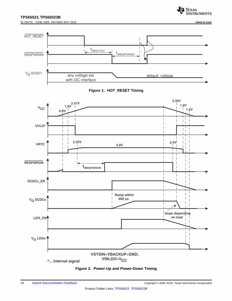
UVLO*
VRTC
VSYSIN=VBACKUP=GND;VINLDO=VCC
tNRESPWRON
DCDCx_EN
VO DCDCx
*... internal signal
0.8V
1.9V
2.52V3.0V
Ramp within800 μs
LDO_EN
slope dependingon load
2.47V
VO LDOx
2.4V
2.35V
1.2V
1.9V
RESPWRON
14
TPS65023, TPS65023BSLVS670L –JUNE 2006–REVISED MAY 2018 www.ti.com
Product Folder Links: TPS65023 TPS65023B
Submit Documentation Feedback Copyright © 2006–2018, Texas Instruments Incorporated
Figure 1. HOT_RESET Timing
Figure 2. Power-Up and Power-Down Timing

CLK
DATA
STA STA STOSTO
th(STA)
t(BUF)
t(LOW)
tr tf
th(DATA)tsu(DATA)
tsu(STA)
th(STA)
tsu(STO)t(HIGH)
15
TPS65023, TPS65023Bwww.ti.com SLVS670L –JUNE 2006–REVISED MAY 2018
Product Folder Links: TPS65023 TPS65023B
Submit Documentation FeedbackCopyright © 2006–2018, Texas Instruments Incorporated
Figure 3. DVS Timing
Figure 4. Serial I/F Timing Diagram
0
10
20
30
40
50
60
70
80
90
100
0.01 0.1 1 10 100 1 k 10 k
I - Output Current - mAO
Eff
icie
ncy -
%
T = 25°C
V = 1.8 V
PWM Mode
A
O
V = 4.2 VI
V = 2.5 VI
V = 3.6 VI
V = 5 VI
0
10
20
30
40
50
60
70
80
90
100
0.01 0.1 1 10 100 1 k 10 k
I - Output Current - mAO
Eff
icie
ncy -
%
T = 25°C
V = 1.8 V
PWM/PFM Mode
A
O
V = 4.2 VI
V = 2.5 VI
V = 3.6 VI
V = 5 VI
0
10
20
30
40
50
60
70
80
90
100
0.01 0.1 1 10 100 1 k 10 k
I - Output Current - mAO
Eff
icie
nc
y -
%
T = 25°C
V = 1.2 V
PWM Mode
A
O
V = 4.2 VI
V = 2.5 VI
V = 3.6 VI
V = 5 VI
0
10
20
30
40
50
60
70
80
90
100
0.01 0.1 1 10 100 1 k 10 k
I - Output Current - mAO
Eff
icie
ncy -
%
T = 25°C
V = 1.2 V
PWM/PFM Mode
A
O
V = 4.2 VI
V = 2.5 VI
V = 3.6 VI
V = 5 VI
16
TPS65023, TPS65023BSLVS670L –JUNE 2006–REVISED MAY 2018 www.ti.com
Product Folder Links: TPS65023 TPS65023B
Submit Documentation Feedback Copyright © 2006–2018, Texas Instruments Incorporated
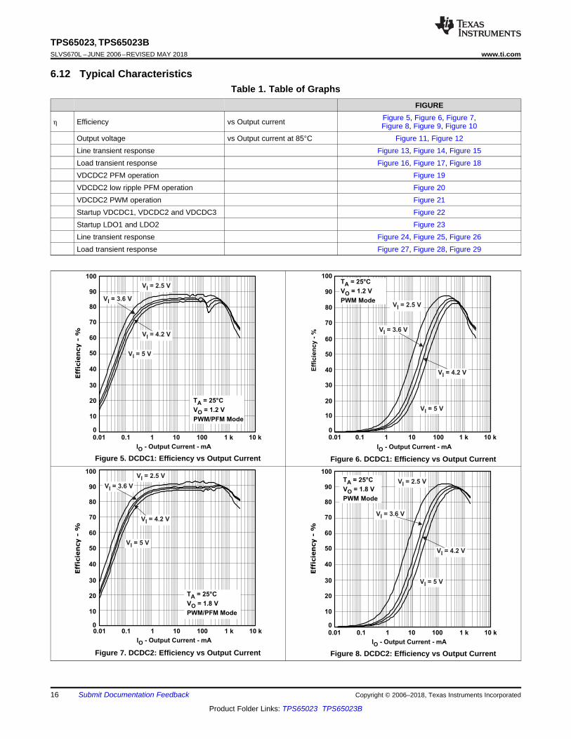
6.12 Typical CharacteristicsTable 1. Table of Graphs
FIGURE
η Efficiency vs Output current Figure 5, Figure 6, Figure 7,Figure 8, Figure 9, Figure 10
Output voltage vs Output current at 85°C Figure 11, Figure 12Line transient response Figure 13, Figure 14, Figure 15Load transient response Figure 16, Figure 17, Figure 18VDCDC2 PFM operation Figure 19VDCDC2 low ripple PFM operation Figure 20VDCDC2 PWM operation Figure 21Startup VDCDC1, VDCDC2 and VDCDC3 Figure 22Startup LDO1 and LDO2 Figure 23Line transient response Figure 24, Figure 25, Figure 26Load transient response Figure 27, Figure 28, Figure 29
Figure 5. DCDC1: Efficiency vs Output Current Figure 6. DCDC1: Efficiency vs Output Current
Figure 7. DCDC2: Efficiency vs Output Current Figure 8. DCDC2: Efficiency vs Output Current

C2 Pk-Pk48.9 mV
C2 Mean1.81053 V
C1 High4.01 V
C1 Low3.02 V
VINDCDC2
VDCDC2
I = 100 mA
VINDCDC2 = 3 V - 4 VDEFDCDC2 = GNDPWW Mode
O
C1 High4.71 V
C1 Low3.68 V
C2 Pk-Pk28.5 mV
C2 Mean1.18925 V
VINDCDC1
VDCDC1
I = 100 mA
VINDCDC1 = 3.7 V - 4.7 VDEFDCDC1 = VINDCDC1PWW Mode
O
3.234
3.254
3.274
3.294
3.314
3.334
3.354
0.1 1 10I - Output Current - AO
V-
Ou
tpu
t V
olt
ag
e -
VO
T = 85°C
DEFDCDC2 = VINDCDC2A
V = 3.8 VI
V = 3.7 VI
V = 3.6 VIV = 3.5 VI
3.234
3.254
3.274
3.294
3.314
3.334
3.354
I - Output Current - AO
V-
Ou
tpu
t V
olt
ag
e -
VO
T = 85°C
DEFDCDC3 = VINDCDC3A
V = 3.8 VI
V = 3.7 VI
V = 3.6 VI
0.1 1 10
V = 4 VI
V = 3.9 VI
V = 3.5 VI
0
10
20
30
40
50
60
70
80
90
100
0.01 0.1 1 10 100 1 k 10 k
I - Output Current - mAO
Eff
icie
ncy -
%
T = 25°C
V = 1.8 V
PWM/PFM Mode
A
O
V = 4.2 VI
V = 2.5 VI
V = 3.6 VI
V = 5 VI
0
10
20
30
40
50
60
70
80
90
100
0.01 0.1 1 10 100 1 k 10 k
I - Output Current - mAO
Eff
icie
ncy -
%
T = 25°C
V = 1.8 V
PWM Mode
A
O
V = 4.2 VI
V = 2.5 VI
V = 3.6 VI
V = 5 VI
17
TPS65023, TPS65023Bwww.ti.com SLVS670L –JUNE 2006–REVISED MAY 2018
Product Folder Links: TPS65023 TPS65023B
Submit Documentation FeedbackCopyright © 2006–2018, Texas Instruments Incorporated
Figure 9. DCDC3: Efficiency vs Output Current Figure 10. DCDC3: Efficiency vs Output Current
Figure 11. DCDC2: Output Voltagevs Output Current at 85°C
Figure 12. DCDC3: Output Voltagevs Output Current at 85°C
Figure 13. VDCDC1 Line Transient Response Figure 14. VDCDC2 Line Transient Response
VDCDC3 = 3.3 V @ 50 mV/Div(AC Coupled)
ILOAD @ 500 mA/Div
100 mA
800 mA
VIN = 3.8 V TIMESCALE = 50 s/Divm
C1 High4.20 V
C1 Low3.59 V
C2 Pk-Pk60.4 mV
C2 Mean3.28264 V
VINDCDC3
VDCDC3
I = 100 mA
VINDCDC3 = 3.6 V - 4.2 VDEFDCDC3 = VINDCDC3PWW Mode
O
18
TPS65023, TPS65023BSLVS670L –JUNE 2006–REVISED MAY 2018 www.ti.com
Product Folder Links: TPS65023 TPS65023B
Submit Documentation Feedback Copyright © 2006–2018, Texas Instruments Incorporated
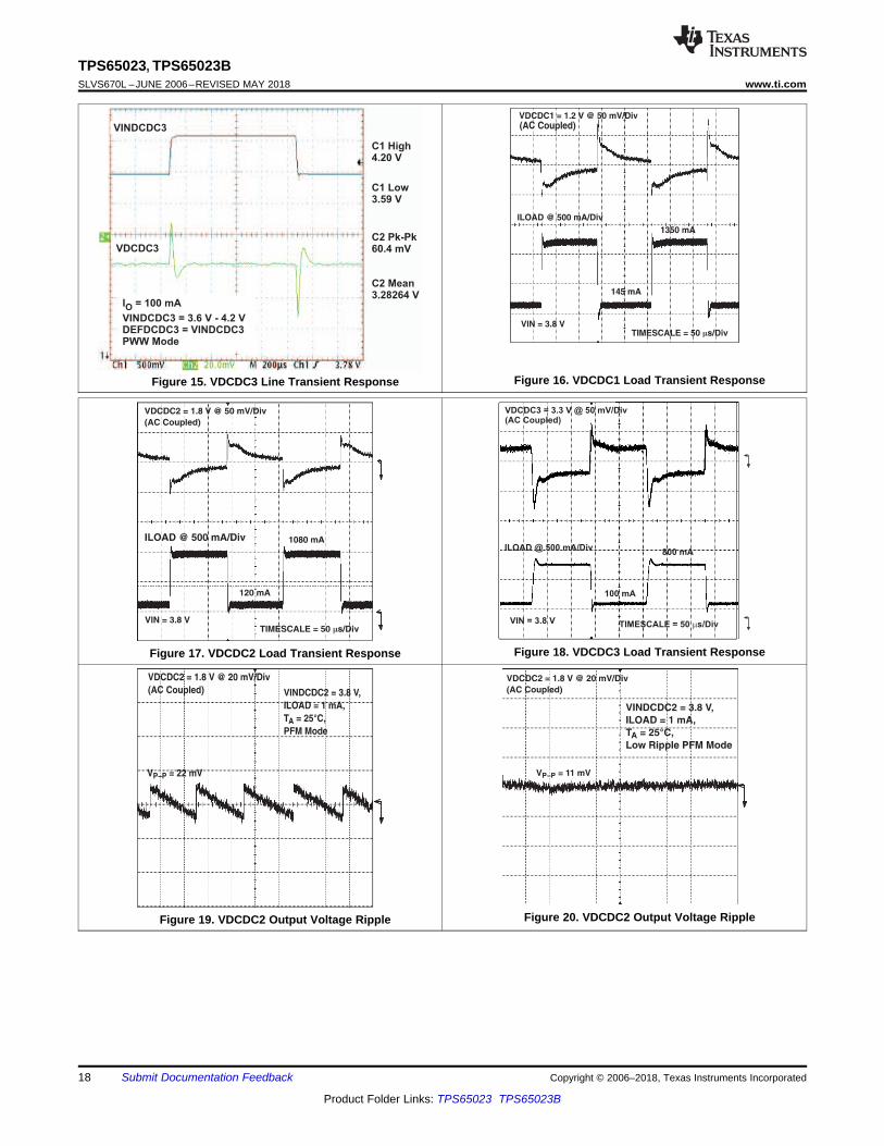
Figure 15. VDCDC3 Line Transient Response Figure 16. VDCDC1 Load Transient Response
Figure 17. VDCDC2 Load Transient Response Figure 18. VDCDC3 Load Transient Response
Figure 19. VDCDC2 Output Voltage Ripple Figure 20. VDCDC2 Output Voltage Ripple
C1 High4.51 V
C1 Low3.99 V
C2 PK-PK6.1 mV
=Ch1 V
Ch2 VI
O=
I = 25 mA
V = 3.3 V
T = 25 C
O
O
Ao
C2 Mean3.29828 V
C1 High3.82 V
C1 Low3.28 V
C2 PK-PK22.8 mV
=Ch1 V
Ch2 VI
O=
I = 10 mA
V = 3 V
T = 25 C
O
O
Ao
C2 Mean2.98454 V
ENABLE
LDO1
LDO2
C1 High3.83 V
C1 Low3.29 V
C2 PK-PK6.2 mV
C2 Mean1.09702 V
=Ch1 V
Ch2 VI
O=
I = 25 mA
V = 1.1 V
T = 25 C
O
O
Ao
mV
19
TPS65023, TPS65023Bwww.ti.com SLVS670L –JUNE 2006–REVISED MAY 2018
Product Folder Links: TPS65023 TPS65023B
Submit Documentation FeedbackCopyright © 2006–2018, Texas Instruments Incorporated
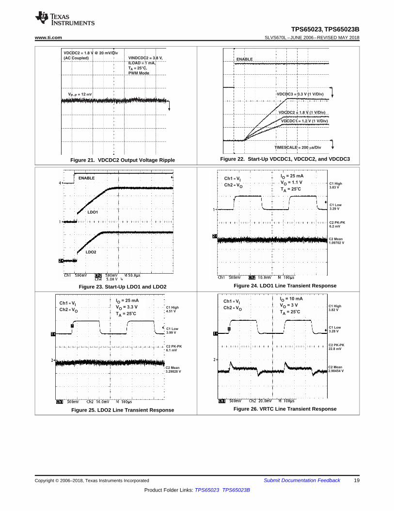
Figure 21. VDCDC2 Output Voltage Ripple Figure 22. Start-Up VDCDC1, VDCDC2, and VDCDC3
Figure 23. Start-Up LDO1 and LDO2 Figure 24. LDO1 Line Transient Response
Figure 25. LDO2 Line Transient Response Figure 26. VRTC Line Transient Response

C4 High21.4 mA
C4 Low-1.4 mA
C2 PK-PK76 mV
=Ch2 V
Ch4 IO
O=
VI
O
A
= 3.8 V
V = 3 V
T = 25 Co
C2 Mean2.9762 V
C4 High48.9 mA
C4 Low2.1 mA
C2 PK-PK42.5 mV
=Ch2 V
Ch4O
O= I
VI
O
A
= 3.3 V
V = 1.1 V
T = 25 Co
C2 Mean1.09664 V
C4 High47.8 mA
C4 Low-2.9 mA
C2 PK-PK40.4 mV
=Ch2 V
Ch4 IO
O=
VI
O
A
= 4 V
V = 3.3 V
T = 25 Co
C2 Mean3.29821 V
20
TPS65023, TPS65023BSLVS670L –JUNE 2006–REVISED MAY 2018 www.ti.com
Product Folder Links: TPS65023 TPS65023B
Submit Documentation Feedback Copyright © 2006–2018, Texas Instruments Incorporated
Figure 27. LDO1 Load Transient Response Figure 28. LDO2 Load Transient Response
Figure 29. VRTC Load Transient Response

21
TPS65023, TPS65023Bwww.ti.com SLVS670L –JUNE 2006–REVISED MAY 2018
Product Folder Links: TPS65023 TPS65023B
Submit Documentation FeedbackCopyright © 2006–2018, Texas Instruments Incorporated
7 Detailed Description
7.1 OverviewTPS65023x has 5 regulator channels, 3 DCDCs and 2 LDOs. DCDC3 has dynamic voltage scaling feature (DVS)that allows for power reduction to CORE supplies during idle operation or overvoltage during heavy-dutyoperation. With DVS and 2 more DCDCs plus 2 LDOs, the TPS65023x is ideal for CORE, Memory, IO, andperipheral power for the entire system of a wide range of suitable applications.
The device incorporates enables for the DCDCs and LDOs, I2C for device control, push button, and a resetinterface that complete the system and allow the TPS65023x to be adapted for different kinds of processors orFPGAs.
For noise-sensitive circuits, the DCDCs can be synchronized out of phase from one another, reducing the peaknoise at the switching frequency. Each converter can be forced to operate in PWM mode to ensure constantswitching frequency across the entire load range. However, for low load efficiency performance the DCDCsautomatically enter PSM mode which reduces the switching frequency when the load current is low, savingpower at idle operation.

TPS65023, TPS65023B
LOW_BATT
VCC
HOT_RESET
INT
RESPWRON
VINDCDC1
DCDC1_EN
PWRFAIL
BBATSWITCH
Serial Interface
CONTROL
UVLOVREFOSC
ThermalShutdown
DCDC1Buck Converter
1700 mA
DCDC2Buck Converter
1200 mA
DCDC3Buck Converter
1000 mA
LDO1200 mA
LDO2200 mA
DynamicVoltage
Management
VSYSIN
VBACKUP
VRTC
SCLK
SDAT
DCDC2_EN
DCDC3_EN
LDO_EN
LOWBAT_SNS
PWRFAIL_SNS
TRESPWRON
DEFLDO1
DEFLDO2
L1
VDCDC1
DEFDCDC1
PGND1
VINDCDC2
L2
VDCDC2
DEFDCDC2
PGND2
VINDCDC3
L3
VDCDC3
DEFDCDC3
PGND3
AGND1
VLDO1
AGND2
VINLDO
VLDO2
22
TPS65023, TPS65023BSLVS670L –JUNE 2006–REVISED MAY 2018 www.ti.com
Product Folder Links: TPS65023 TPS65023B
Submit Documentation Feedback Copyright © 2006–2018, Texas Instruments Incorporated
7.2 Functional Block Diagram
7.3 Feature Description
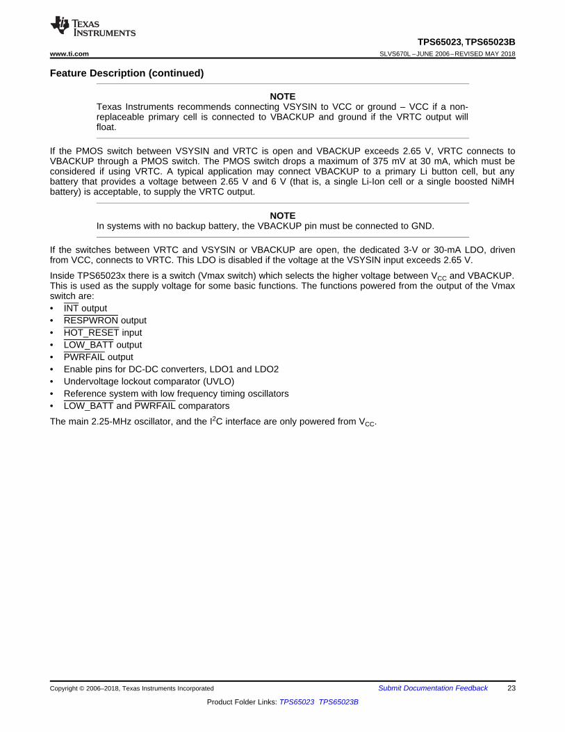
7.3.1 VRTC Output and Operation With or Without Backup BatteryThe VRTC pin is an always-on output, intended to supply up to 30 mA to a permanently required rail (that is, fora real time clock). The TPS65023x asserts the RESPWRON signal if VRTC drops below 2.4 V. VRTC is selectedfrom a priority scheme based on the VSYSIN and VBACKUP inputs.
When the voltage at the VSYSIN pin exceeds 2.65 V, VRTC connects to the VSYSIN input through a PMOSswitch and all other paths to VRTC are disabled. The PMOS switch drops a maximum of 375 mV at 30 mA,which must be considered when using VRTC. VSYSIN can be connected to any voltage source with theappropriate input voltage, including VCC or, if set to 3.3-V output, DCDC2 or DCDC3. When VSYSIN falls below2.65 V or shorts to ground, the PMOS switch connecting VRTC and VSYSIN opens and VRTC then connects toeither VBACKUP or the output of a dedicated 3-V or 30-mA LDO.
23
TPS65023, TPS65023Bwww.ti.com SLVS670L –JUNE 2006–REVISED MAY 2018
Product Folder Links: TPS65023 TPS65023B
Submit Documentation FeedbackCopyright © 2006–2018, Texas Instruments Incorporated
Feature Description (continued)
NOTETexas Instruments recommends connecting VSYSIN to VCC or ground – VCC if a non-replaceable primary cell is connected to VBACKUP and ground if the VRTC output willfloat.
If the PMOS switch between VSYSIN and VRTC is open and VBACKUP exceeds 2.65 V, VRTC connects toVBACKUP through a PMOS switch. The PMOS switch drops a maximum of 375 mV at 30 mA, which must beconsidered if using VRTC. A typical application may connect VBACKUP to a primary Li button cell, but anybattery that provides a voltage between 2.65 V and 6 V (that is, a single Li-Ion cell or a single boosted NiMHbattery) is acceptable, to supply the VRTC output.
NOTEIn systems with no backup battery, the VBACKUP pin must be connected to GND.
If the switches between VRTC and VSYSIN or VBACKUP are open, the dedicated 3-V or 30-mA LDO, drivenfrom VCC, connects to VRTC. This LDO is disabled if the voltage at the VSYSIN input exceeds 2.65 V.
Inside TPS65023x there is a switch (Vmax switch) which selects the higher voltage between VCC and VBACKUP.This is used as the supply voltage for some basic functions. The functions powered from the output of the Vmaxswitch are:• INT output• RESPWRON output• HOT_RESET input• LOW_BATT output• PWRFAIL output• Enable pins for DC-DC converters, LDO1 and LDO2• Undervoltage lockout comparator (UVLO)• Reference system with low frequency timing oscillators• LOW_BATT and PWRFAIL comparators
The main 2.25-MHz oscillator, and the I2C interface are only powered from VCC.
RESPWRON
VRTC
LDO
VCC
VRTC
Vref
Vref Vref
priority
#3
priority
#2
priority
#1
ENV_VSYSIN
V_VBACKUP
VBACKUP
V_VBACKUP
VSYSIN
V_VSYSIN
24
TPS65023, TPS65023BSLVS670L –JUNE 2006–REVISED MAY 2018 www.ti.com
Product Folder Links: TPS65023 TPS65023B
Submit Documentation Feedback Copyright © 2006–2018, Texas Instruments Incorporated
Feature Description (continued)
A. V_VSYSIN, V_VBACKUP thresholds: falling = 2.55 V, rising = 2.65 V ±3%B. RESPWRON thresholds: falling = 2.4 V, rising = 2.52 V ±3%
Figure 30. RTC and nRESPWRON
7.3.2 Step-Down Converters, VDCDC1, VDCDC2, and VDCDC3The TPS65023x incorporates three synchronous step-down converters operating typically at2.25-MHz, fixed frequency pulse width modulation (PWM) at moderate to heavy-load currents. At light-loadcurrents, the converters automatically enter the power save mode (PSM), and operate with pulse frequencymodulation (PFM). The VDCDC1 converter is capable of delivering 1.5-A output current, the VDCDC2 converteris capable of delivering 1.2 A and the VDCDC3 converter is capable of delivering up to 1 A.
The converter output voltages can be programmed through the DEFDCDC1, DEFDCDC2, and DEFDCDC3 pins.The pins can either be connected to GND, VCC, or to a resistor divider between the output voltage and GND.The VDCDC1 converter defaults to 1.2 V or 1.6 V depending on the DEFDCDC1 configuration pin. If DEFDCDC1is tied to ground, the default is 1.2 V. If it is tied to VCC, the default is 1.6 V. When the DEFDCDC1 pin isconnected to a resistor divider, the output voltage can be set in the range of 0.6 V to VINDCDC1 V. SeeApplication Information for more details. The core voltage can be reprogrammed through the serial interface inthe range of 0.8 V to 1.6 V with a programmable slew rate. The converter is forced into PWM operation whilstany programmed voltage change is underway, whether the voltage is being increased or decreased. TheDEFCORE and DEFSLEW registers are used to program the output voltage and slew rate during voltagetransitions.
The VDCDC2 converter defaults to 1.8 V or 3.3 V depending on the DEFDCDC2 configuration pin. If DEFDCDC2is tied to ground, the default is 1.8 V. If it is tied to VCC, the default is 3.3 V. When the DEFDCDC2 pin isconnected to a resistor divider, the output voltage can be set in the range of 0.6 V to VINDCDC2 V.
The VDCDC3 converter defaults to 1.8 V or 3.3 V depending on the DEFDCDC3 configuration pin. If DEFDCDC3is tied to ground the default is 1.8 V. If it is tied to VCC, the default is 3.3 V. When the DEFDCDC3 pin isconnected to a resistor divider, the output voltage can be set in the range of 0.6 V to VINDCDC3 V.
The step-down converter outputs (when enabled) are monitored by power-good (PG) comparators, the outputs ofwhich are available through the serial interface. The outputs of the DC-DC converters can be optionallydischarged through on-chip 300-Ω resistors when the DC-DC converters are disabled.
PFMDCDC3
VINDCDC3I leave =
29 W
PFMDCDC2
VINDCDC2I leave =
20 W
PFMDCDC1
VINDCDC1I leave =
18 W
PFMDCDC3
VINDCDC3I enter =
39 W
PFMDCDC2
VINDCDC2I enter =
26 Ω
PFMDCDC1
VINDCDCI enter =
24 Ω
1
25
TPS65023, TPS65023Bwww.ti.com SLVS670L –JUNE 2006–REVISED MAY 2018
Product Folder Links: TPS65023 TPS65023B
Submit Documentation FeedbackCopyright © 2006–2018, Texas Instruments Incorporated
Feature Description (continued)During PWM operation, the converters use a unique fast response voltage mode controller scheme with inputvoltage feedforward to achieve good line and load regulation allowing the use of small ceramic input and outputcapacitors. At the beginning of each clock cycle initiated by the clock signal, the P-channel MOSFET switch isturned on. The inductor current ramps up until the comparator trips and the control logic turns off the switch. Thecurrent limit comparator also turns off the switch if the current limit of the P-channel switch is exceeded. After theadaptive dead-time used to prevent shoot through current, the N-channel MOSFET rectifier is turned on, and theinductor current ramps down. The next cycle is initiated by the clock signal, again turning off the N-channelrectifier and turning on the P-channel switch.
The three DC-DC converters operate synchronized to each other with the VDCDC1 converter as the master. A180° phase shift between the VDCDC1 switch turn on and the VDCDC2 and a further 90° shift to the VDCDC3switch turn on decreases the input RMS current and smaller input capacitors can be used. This is optimized for atypical application where the VDCDC1 converter regulates a Li-Ion battery voltage of 3.7 V to 1.2 V, theVDCDC2 converter from 3.7 V to 1.8 V, and the VDCDC3 converter from 3.7 V to 3.3 V. The phase of the threeconverters can be changed using the CON_CTRL register.
7.3.3 Power Save Mode OperationAs the load current decreases, the converters enter the power save mode operation. During PSM, the convertersoperate in a burst mode (PFM mode) with a frequency between 750 kHz and 2.25 MHz, nominal for one burstcycle. However, the frequency between different burst cycles depends on the actual load current and is typicallyfar less than the switching frequency with a minimum quiescent current to maintain high efficiency.
To optimize the converter efficiency at light load, the average current is monitored and if in PWM mode theinductor current remains below a certain threshold, then PSM is entered. The typical threshold to enter PSM iscalculated as shown in Equation 1, Equation 2 and Equation 3.
(1)
(2)
(3)
During the PSM the output voltage is monitored with a comparator, and by maximum skip burst width. As theoutput voltage falls below the threshold, set to the nominal VO, the P-channel switch turns on and the convertereffectively delivers a constant current defined in Equation 4, Equation 5 and Equation 6.
(4)
(5)
(6)
If the load is below the delivered current then the output voltage rises until the same threshold is crossed in theother direction. All switching activity ceases, reducing the quiescent current to a minimum until the output voltagehas again dropped below the threshold. The power save mode is exited, and the converter returns to PWM modeif either of the following conditions are met:1. the output voltage drops 2% below the nominal VO due to increasing load current2. the PFM burst time exceeds 16 × 1/fs (7.11 μs typical).
These control methods reduce the quiescent current to typically 14 μA per converter, and the switching activity toa minimum, thus achieving the highest converter efficiency. Setting the comparator thresholds at the nominaloutput voltage at light-load current results in a low output voltage ripple. The ripple depends on the comparatordelay and the size of the output capacitor. Increasing capacitor values makes the output ripple tend to zero. ThePSM is disabled through the I2C interface to force the individual converters to stay in fixed frequency PWMmode.
min min max DS(on) LVin Vout Iout r max R u
26
TPS65023, TPS65023BSLVS670L –JUNE 2006–REVISED MAY 2018 www.ti.com
Product Folder Links: TPS65023 TPS65023B
Submit Documentation Feedback Copyright © 2006–2018, Texas Instruments Incorporated
Feature Description (continued)7.3.4 Low Ripple ModeSetting bit 3 in register CON-CTRL to 1 enables the low ripple mode for all of the DC-DC converters if operatedin PFM mode. For an output current less than approximately 10 mA, the output voltage ripple in PFM mode isreduced, depending on the actual load current. The lower the actual output current on the converter, the lowerthe output ripple voltage. For an output current above 10 mA, there is only minor difference in output voltageripple between PFM mode and low ripple PFM mode. As this feature also increases switching frequency, it isused to keep the switching frequency above the audible range in PFM mode down to a low output current.
7.3.5 Soft-StartEach of the three converters has an internal soft-start circuit that limits the inrush current during start-up. Thesoft-start is realized by using a low current to initially charge the internal compensation capacitor. The soft-starttime is typically 750 μs if the output voltage ramps from 5% to 95% of the final target value. If the output isalready precharged to some voltage when the converter is enabled, then this time is reduced proportionally.There is a short delay of typically 170 μs between the converter being enabled and switching activity actuallystarting. This allows the converter to bias itself properly, to recognize if the output is precharged, and if so toprevent discharging of the output while the internal soft-start ramp catches up with the output voltage.
7.3.6 100% Duty Cycle Low Dropout OperationThe TPS65023x converters offer a low input to output voltage difference while still maintaining operation with theuse of the 100% duty cycle mode. In this mode the P-channel switch is constantly turned on. This is particularlyuseful in battery-powered applications to achieve longest operation time by taking full advantage of the wholebattery voltage range. The minimum input voltage required to maintain DC regulation depends on the loadcurrent and output voltage. It is calculated in Equation 7.
where• Ioutmax = maximum load current (Note: ripple current in the inductor is zero under these conditions)• rDS(on)max = maximum P-channel switch rDS(on)
• RL = DC resistance of the inductor• Voutmin = nominal output voltage minus 2% tolerance limit (7)
7.3.7 Active Discharge When DisabledWhen the VDCDC1, VDCDC2, and VDCDC3 converters are disabled, due to an UVLO, DCDC_EN orOVERTEMP condition, it is possible to actively pull down the outputs. This feature is disabled per default and isindividually enabled through the CON_CTRL2 register in the serial interface. When this feature is enabled, theVDCDC1, VDCDC2, and VDCDC3 outputs are discharged by a 300-Ω (typical) load which is active as long asthe converters are disabled.
7.3.8 Power-Good MonitoringAll three step-down converters and both the LDO1 and LDO2 linear regulators have power-good comparators.Each comparator indicates when the relevant output voltage has dropped 10% below its target value with 5%hysteresis. The outputs of these comparators are available in the PGOODZ register through the serial interface.An interrupt is generated when any voltage rail drops below the 10% threshold. The comparators are disabledwhen the converters are disabled and the relevant PGOODZ register bits indicate that power is good.

27
TPS65023, TPS65023Bwww.ti.com SLVS670L –JUNE 2006–REVISED MAY 2018
Product Folder Links: TPS65023 TPS65023B
Submit Documentation FeedbackCopyright © 2006–2018, Texas Instruments Incorporated
Feature Description (continued)7.3.9 Low-Dropout Voltage RegulatorsThe low-dropout voltage regulators are designed to operate well with low-value ceramic input and outputcapacitors. They operate with input voltages down to 1.5 V. The LDOs offer a maximum dropout voltage of300 mV at rated output current. Each LDO supports a current limit feature. Both LDOs are enabled by theLDO_EN pin, both LDOs can be disabled or programmed through the serial interface using the REG_CTRL andLDO_CTRL registers. The LDOs also have reverse conduction prevention. This allows the possibility to connectexternal regulators in parallel in systems with a backup battery. The TPS65023x step-down and LDO voltageregulators automatically power down when the VCC voltage drops below the UVLO threshold or when the junctiontemperature rises above 160°C.
7.3.10 Undervoltage LockoutThe undervoltage lockout circuit for the five regulators on the TPS65023x prevents the device frommalfunctioning at low-input voltages and from excessive discharge of the battery. It disables the converters andLDOs. The UVLO circuit monitors the VCC pin, the threshold is set internally to 2.35 V with 5% (120 mV)hysteresis. When any of the DC-DC converters are running, there is an input current at the VCC pin, which is upto 3 mA when all three converters are running in PWM mode. Consider this current if an external RC filter is usedat the VCC pin to remove switching noise from the TPS65023x internal analog circuitry supply.
7.3.11 Power-Up SequencingThe TPS65023x power-up sequencing is designed to be entirely flexible and customer driven. This is achievedby providing separate enable pins for each switch-mode converter, and a common enable signal for the LDOs.The relevant control pins are described in Table 2.
Table 2. Control Pins and Status Outputs for DC–DC ConvertersPIN NAME I/O FUNCTION
DEFDCDC3 I Defines the default voltage of the VDCDC3 switching converter. DEFDCDC3 = 0 defaults VDCDC3 to 1.8 V,DEFDCDC3 = VCC defaults VDCDC3 to 3.3 V.
DEFDCDC2 I Defines the default voltage of the VDCDC2 switching converter. DEFDCDC2 = 0 defaults VDCDC2 to 1.8 V,DEFDCDC2 = VCC defaults VDCDC2 to 3.3 V.
DEFDCDC1 I Defines the default voltage of the VDCDC1 switching converter. DEFDCDC1 = 0 defaults VDCDC1 to 1.2 V,DEFDCDC1 = VCC defaults VDCDC1 to 1.6 V.
DCDC3_EN I Set DCDC3_EN = 0 to disable and DCDC3_EN = 1 to enable the VDCDC3 converterDCDC2_EN I Set DCDC2_EN = 0 to disable and DCDC2_EN = 1 to enable the VDCDC2 converterDCDC1_EN I Set DCDC1_EN = 0 to disable and DCDC1_EN = 1 to enable the VDCDC1 converter
HOT_RESET IThe HOT_RESET pin generates a reset (RESPWRON) for the processor.HOT_RESET does not alter anyTPS65023x settings except the output voltage of VDCDC1. Activating HOT_RESET sets the voltage of VDCDC1to its default value defined with the DEFDCDC1 pin. HOT_RESET is internally de-bounced by the TPS65023x.
RESPWRON ORESPWRON is held low when power is initially applied to the TPS65023x. The VRTC voltage is monitored:RESWPRON is low when VRTC < 2.4 V and remains low for a time defined by the external capacitor at theTRESPWRON pin. RESPWRON can also be forced low by activation of the HOT_RESET pin.
TRESPWRON I Connect a capacitor here to define the RESET time at the RESPWRON pin (1 nF typically gives 100 ms).
7.4 Device Functional ModesThe TPS6502x devices are either in the ON or the OFF mode. The OFF mode is entered when the voltage onVCC is below the UVLO threshold, 2.35 V (typically). Once the voltage at VCC has increased above UVLO, thedevice enters ON mode. In the ON mode, the DCDCs and LDOs are available for use.
28
TPS65023, TPS65023BSLVS670L –JUNE 2006–REVISED MAY 2018 www.ti.com
Product Folder Links: TPS65023 TPS65023B
Submit Documentation Feedback Copyright © 2006–2018, Texas Instruments Incorporated
7.5 Programming
7.5.1 System Reset + Control SignalsThe RESPWRON signal can be used as a global reset for the application. It is an open-drain output. TheRESPWRON signal is generated according to the power-good comparator of VRTC, and remains low for tnrespwronseconds after VRTC has risen above 2.52 V (falling threshold is 2.4 V, 5% hysteresis). tnrespwron is set by anexternal capacitor at the TRESPWRON pin. 1 nF gives typically 100 ms. RESPWRON is also triggered by theHOT_RESET input. This input is internally debounced, with a filter time of typically 30 ms.
The PWRFAIL and LOW_BAT signals are generated by two voltage detectors using the PWRFAIL_SNS andLOWBAT_SNS input signals. Each input signal is compared to a 1-V threshold (falling edge) with 5% (50 mV)hysteresis.
The DCDC1 converter is reset to its default output voltage defined by the DEFDCDC1 input, when HOT_RESETis asserted. Other I2C registers are not affected. Generally, the DCDC1 converter is set to its default voltage withone of these conditions: HOT_RESET active, VRTC lower than its threshold voltage, undervoltage lockout(UVLO) condition, or RESPWRON active.
7.5.1.1 DEFLDO1 and DEFLDO2These two pins are used to set the default output voltage of the two 200-mA LDOs. The digital value applied tothe pins is latched during power up and determines the initial output voltage according to Table 3. The voltage ofboth LDOs can be changed during operation with the I2C interface as described in the interface description.
Table 3. LDO1 and LDO2 Default Voltage OptionsDEFLDO2 DEFLDO1 VLDO1 VLDO2
0 0 1.3 V 3.3 V0 1 2.8 V 3.3 V1 0 1.3 V 1.8 V1 1 1.8 V 3.3 V
7.5.1.2 Interrupt Management and the INT PinThe INT pin combines the outputs of the PGOOD comparators from each DC–DC converter and the LDOs. TheINT pin is used as a POWER_OK pin to indicate when all enabled supplies are in regulation. The INT pinremains active (low state) during power up as long as all enabled power rails are below their regulation limit.Once the last enabled power rail is within regulation, the INT pin transitions to a high state.
During operation, if one of the enabled supplies goes out of regulation, INT transitions to a low state, and thecorresponding bit in the PGOODZ register goes high. If the supply goes back to its regulation limits, INTtransitions back to a high state.
While INT is in an active-low state, reading the PGOODZ register through the I2C bus forces INT into a high-Zstate. Because this pin requires an external pullup resistor, the INT pin transitions to a logic high state eventhough the supply in question is still out of regulation. The corresponding bit in the PGOODZ register stillindicates that the power rail is out of regulation.
Interrupts can be masked using the MASK register; default operation is not to mask any DCDC or LDO interruptsbecause this provides the POWER_OK function. If none of the DCDC converters or LDos are enabled, /INTdefaults to a low state independently of the settings of the MASK register.
7.5.2 Serial InterfaceThe serial interface is compatible with the standard and fast mode I2C specifications, allowing transfers at up to400 kHz. The interface adds flexibility to the power supply solution, enabling most functions to be programmed tonew values depending on the instantaneous application requirements and charger status to be monitored.Register contents remain intact as long as VCC remains above 2 V. The TPS65023x has a 7-bit address:1001000, other addresses are available upon contact with the factory. Attempting to read data from the registeraddresses not listed in this section results in FFh being read out.

SCLK
SDAT
Start Slave Address Register Address Data
0
A6 A5 A4 A0 R/W R7 R6 R5 R0 D7 D6 D5 D0ACK ACK ACK
0 0 0
Stop
Note: SLAVE = TPS65023
DATA
CLK
CE
S P
START Condition STOP Condition
Data LineStable;
Data Valid
DATA
CLK
Changeof DataAllowed
29
TPS65023, TPS65023Bwww.ti.com SLVS670L –JUNE 2006–REVISED MAY 2018
Product Folder Links: TPS65023 TPS65023B
Submit Documentation FeedbackCopyright © 2006–2018, Texas Instruments Incorporated
For normal data transfer, DATA is allowed to change only when CLK is low. Changes when CLK is high arereserved for indicating the start and stop conditions. During data transfer, the data line must remain stablewhenever the clock line is high. There is one clock pulse per bit of data. Each data transfer is initiated with a startcondition and terminated with a stop condition. When addressed, the TPS65023x device generates anacknowledge bit after the reception of each byte. The master device (microprocessor) must generate an extraclock pulse that is associated with the acknowledge bit. The TPS65023x device must pull down the DATA lineduring the acknowledge clock pulse so that the DATA line is a stable low during the high period of theacknowledge clock pulse. The DATA line is a stable low during the high period of the acknowledge–related clockpulse. Setup and hold times must be taken into account. During read operations, a master must signal the end ofdata to the slave by not generating an acknowledge bit on the last byte that was clocked out of the slave. In thiscase, the slave TPS65023x device must leave the data line high to enable the master to generate the stopcondition. See I2C Timing Requirements for TPS65023B for more information.
Figure 31. Bit Transfer on the Serial Interface
Figure 32. START and STOP Conditions
Figure 33. Serial I/F WRITE to TPS65023x Device

SCLK
SDA
Start
Stop StartSlaveDrives
the Data
MasterDrives
ACK and Stop
Slave Address Slave AddressRegisterAddress
0 0 0 01Stop
Note: SLAVE = TPS65023
A6A6 A0A0 R/W R/WR7 R0 D7 D0ACK ACKACK ACK
SCLK
SDAT
Start
RepeatedStart
SlaveDrives
the Data
MasterDrives
ACK and Stop
Slave Address Slave AddressRegisterAddress
0
A6A6 A0A0 R/W R/WR7 R0 D7 D0ACK ACKACK ACK
0 0 01
Stop
Note: SLAVE = TPS65023
30
TPS65023, TPS65023BSLVS670L –JUNE 2006–REVISED MAY 2018 www.ti.com
Product Folder Links: TPS65023 TPS65023B
Submit Documentation Feedback Copyright © 2006–2018, Texas Instruments Incorporated
Figure 34. Serial I/F READ from TPS65023x: Protocol A
Figure 35. Serial I/F READ from TPS65023x: Protocol B

31
TPS65023, TPS65023Bwww.ti.com SLVS670L –JUNE 2006–REVISED MAY 2018
Product Folder Links: TPS65023 TPS65023B
Submit Documentation FeedbackCopyright © 2006–2018, Texas Instruments Incorporated
7.6 Register Maps
7.6.1 VERSION Register Address: 00h (Read Only)
Table 4. VERSION RegisterVERSION B7 B6 B5 B4 B3 B2 B1 B0Bit name andfunction
0 0 1 0 0 0 1 1
Read and write R R R R R R R R
7.6.2 PGOODZ Register Address: 01h (Read Only)
Table 5. PGOODZ RegisterPGOODZ B7 B6 B5 B4 B3 B2 B1 B0Bit name andfunction PWRFAILZ LOWBATTZ PGOODZ
VDCDC1PGOODZVDCDC2
PGOODZVDCDC3
PGOODZLDO2
PGOODZLDO1 –
Set by signal PWRFAIL LOWBATT PGOODZVDCDC1
PGOODZVDCDC2
PGOODZVDCDC3
PGOODZLDO2
PGOODZLDO1 –
Default valueloaded PWRFAILZ LOWBATTZ PGOOD
VDCDC1PGOODVDCDC2
PGOODVDCDC3
PGOODLDO2
PGOODLDO1 –
Read and write R R R R R R R R
Bit 7 PWRFAILZ:0 = indicates that the PWRFAIL_SNS input voltage is above the 1-V threshold.1 = indicates that the PWRFAIL_SNS input voltage is below the 1-V threshold.
Bit 6 LOWBATTZ:0 = indicates that the LOWBATT_SNS input voltage is above the 1-V threshold.1 = indicates that the LOWBATT_SNS input voltage is below the 1-V threshold.
Bit 5 PGOODZ VDCDC1:0 = indicates that the VDCDC1 converter output voltage is within its nominal range. This bit is zero if
the VDCDC1 converter is disabled.1 = indicates that the VDCDC1 converter output voltage is below its target regulation voltage
Bit 4 PGOODZ VDCDC2:0 = indicates that the VDCDC2 converter output voltage is within its nominal range. This bit is zero if
the VDCDC2 converter is disabled.1 = indicates that the VDCDC2 converter output voltage is below its target regulation voltage
Bit 3 PGOODZ VDCDC3: .0 = indicates that the VDCDC3 converter output voltage is within its nominal range. This bit is zero if
the VDCDC3 converter is disabled and during a DVM controlled output voltage transition1 = indicates that the VDCDC3 converter output voltage is below its target regulation voltage
Bit 2 PGOODZ LDO2:0 = indicates that the LDO2 output voltage is within its nominal range. This bit is zero if LDO2 is
disabled.1 = indicates that LDO2 output voltage is below its target regulation voltage
Bit 1 PGOODZ LDO10 = indicates that the LDO1 output voltage is within its nominal range. This bit is zero if LDO1 is
disabled.
32
TPS65023, TPS65023BSLVS670L –JUNE 2006–REVISED MAY 2018 www.ti.com
Product Folder Links: TPS65023 TPS65023B
Submit Documentation Feedback Copyright © 2006–2018, Texas Instruments Incorporated
1 = indicates that the LDO1 output voltage is below its target regulation voltage
7.6.3 MASK Register Address: 02h (Read and Write), Default Value: C0h
Table 6. MASK RegisterMASK B7 B6 B5 B4 B3 B2 B1 B0Bit name andfunction
MASKPWRFAILZ
MASKLOWBATTZ
MASKVDCDC1
MASKVDCDC2
MASKVDCDC3
MASKLDO2
MASKLDO1 –
Default 1 1 0 0 0 0 0 0Default valueloaded UVLO UVLO UVLO UVLO UVLO UVLO UVLO –
Read and write R/W R/W R/W R/W R/W R/W R/W –
The MASK register can be used to mask particular fault conditions from appearing at the INT pin. MASK<n> = 1masks PGOODZ<n>.
7.6.4 REG_CTRL Register Address: 03h (Read and Write), Default Value: FFhThe REG_CTRL register is used to disable or enable the power supplies through the serial interface. Thecontents of the register are logically AND’ed with the enable pins to determine the state of the supplies. A UVLOcondition resets the REG_CTRL to 0xFF, so the state of the supplies defaults to the state of the enable pin. TheREG_CTRL bits are automatically reset to default when the corresponding enable pin is low.
Table 7. REG_CTRL RegisterREG_CTRL B7 B6 B5 B4 B3 B2 B1 B0Bit name andfunction – – VDCDC1
ENABLEVDCDC2ENABLE
VDCDC3ENABLE
LDO2ENABLE
LDO1ENABLE –
Default 1 1 1 1 1 1 1 1Set by signal – – DCDC1_ENZ DCDC2_ENZ DCDC3_ENZ LDO_ENZ LDO_ENZ –Default valueloaded – – UVLO UVLO UVLO UVLO UVLO –
Read and write – – R/W R/W R/W R/W R/W –
Bit 5 VDCDC1 ENABLEDCDC1 Enable. This bit is logically AND’ed with the state of the DCDC1_EN pin to turn on the DCDC1converter. Reset to 1 by a UVLO condition, the bit can be written to 0 or 1 through the serial interface.The bit is reset to 1 when the pin DCDC1_EN is pulled to GND, allowing DCDC1 to turn on whenDCDC1_EN returns high.
Bit 4 VDCDC2 ENABLEDCDC2 Enable. This bit is logically AND’ed with the state of the DCDC2_EN pin to turn on the DCDC2converter. Reset to 1 by a UVLO condition, the bit can be written to 0 or 1 through the serial interface.The bit is reset to 1 when the pin DCDC2_EN is pulled to GND, allowing DCDC2 to turn on whenDCDC2_EN returns high.
Bit 3 VDCDC3 ENABLEDCDC3 Enable. This bit is logically AND’ed with the state of the DCDC3_EN pin to turn on the DCDC3converter. Reset to 1 by a UVLO condition, the bit can be written to 0 or 1 through the serial interface.The bit is reset to 1 when the pin DCDC3_EN is pulled to GND, allowing DCDC3 to turn on whenDCDC3_EN returns high.
Bit 2 LDO2 ENABLELDO2 Enable. This bit is logically AND’ed with the state of the LDO2_EN pin to turn on LDO2. Reset to1 by a UVLO condition, the bit can be written to 0 or 1 through the serial interface. The bit is reset to 1when the pin LDO_EN is pulled to GND, allowing LDO2 to turn on when LDO_EN returns high.
33
TPS65023, TPS65023Bwww.ti.com SLVS670L –JUNE 2006–REVISED MAY 2018
Product Folder Links: TPS65023 TPS65023B
Submit Documentation FeedbackCopyright © 2006–2018, Texas Instruments Incorporated
Bit 1 LDO1 ENABLELDO1 Enable. This bit is logically AND’ed with the state of the LDO1_EN pin to turn on LDO1. Reset to1 by a UVLO condition, the bit can be written to 0 or 1 through the serial interface. The bit is reset to 1when the pin LDO_EN is pulled to GND, allowing LDO1 to turn on when LDO_EN returns high.
7.6.5 CON_CTRL Register Address: 04h (Read and Write), Default Value: B1h
Table 8. CON_CTRL RegisterCON_CTRL B7 B6 B5 B4 B3 B2 B1 B0Bit name andfunction
DCDC2PHASE1
DCDC2PHASE0
DCDC3PHASE1
DCDC3PHASE0
LOWRIPPLE
FPWMDCDC2
FPWMDCDC1
FPWMDCDC3
Default 1 0 1 1 0 0 0 0Default valueloaded UVLO UVLO UVLO UVLO UVLO UVLO UVLO UVLO
Read and write R/W R/W R/W R/W R/W R/W R/W R/W
The CON_CTRL register is used to force any or all of the converters into forced PWM operation, when lowoutput voltage ripple is vital. It is also used to control the phase shift between the three converters to minimizethe input rms current, hence reduce the required input blocking capacitance. The DCDC1 converter is taken asthe reference and consequently has a fixed zero phase shift.
Table 9. DCDC2 and DCDC3 Phase Delay
CON_CTRL<7:6> DCDC2 CONVERTERDELAYED BY CON_CTRL<5:4> DCDC3 CONVERTER
DELAYED BY00 zero 00 zero01 1/4 cycle 01 1/4 cycle10 1/2 cycle 10 1/2 cycle11 3/4 cycle 11 3/4 cycle
Bit 3 LOW RIPPLE:0 = PFM mode operation optimized for high efficiency for all converters1 = PFM mode operation optimized for low output voltage ripple for all converters
Bit 2 FPWM DCDC2:0 = DCDC2 converter operates in PWM / PFM mode1 = DCDC2 converter is forced into fixed frequency PWM mode
Bit 1 FPWM DCDC1:0 = DCDC1 converter operates in PWM / PFM mode1 = DCDC1 converter is forced into fixed frequency PWM mode
Bit 0 FPWM DCDC3:0 = DCDC3 converter operates in PWM / PFM mode1 = DCDC3 converter is forced into fixed frequency PWM mode
7.6.6 CON_CTRL2 Register Address: 05h (Read and Write), Default Value: 40h
Table 10. CON_CTRL2 RegisterCON_CTRL2 B7 B6 B5 B4 B3 B2 B1 B0Bit name andfunction GO Core adj
allowed – – – DCDC2discharge
DCDC1discharge
DCDC3discharge
Default 0 1 0 0 0 0 0 0
34
TPS65023, TPS65023BSLVS670L –JUNE 2006–REVISED MAY 2018 www.ti.com
Product Folder Links: TPS65023 TPS65023B
Submit Documentation Feedback Copyright © 2006–2018, Texas Instruments Incorporated
Table 10. CON_CTRL2 Register (continued)CON_CTRL2 B7 B6 B5 B4 B3 B2 B1 B0Default valueloaded
UVLO +DONE RESET(1) – – – UVLO UVLO UVLO
Read and write R/W R/W – – – R/W R/W R/W
The CON_CTRL2 register can be used to take control the inductive converters.
RESET(1): CON_CTRL2[6] is reset to its default value by one of these events:• undervoltage lockout (UVLO)• HOT_RESET pulled low• RESPWRON active• VRTC below threshold
Bit 7 GO:0 = no change in the output voltage for the DCDC1 converter1 = the output voltage of the DCDC1 converter is changed to the value defined in DEFCORE with
the slew rate defined in DEFSLEW. This bit is automatically cleared when the DVM transition iscomplete. The transition is considered complete in this case when the desired output voltagecode has been reached, not when the VDCDC1 output voltage is actually in regulation at thedesired voltage.
Bit 6 CORE ADJ Allowed:0 = the output voltage is set with the I2C register1 = DEFDCDC1 is either connected to GND or VCC or an external voltage divider. When
connected to GND or VCC, VDCDC1 defaults to 1.2 V or 1.6 V respectively at start-upBit 2– 0 0 = the output capacitor of the associated converter is not actively discharged when the converter is
disabled1 = the output capacitor of the associated converter is actively discharged when the converter is
disabled. This decreases the fall time of the output voltage at light load
7.6.7 DEFCORE Register Address: 06h (Read and Write), Default Value: 14h/1Eh
Table 11. DEFCORE RegisterDEFCORE B7 B6 B5 B4 B3 B2 B1 B0Bit name andfunction – – – CORE4 CORE3 CORE2 CORE1 CORE0
Default 0 0 0 1 DEFDCDC1 DEFDCDC1 DEFDCDC1 DEFDCDC1Default valueloaded – – – RESET(1) RESET(1) RESET(1) RESET(1) RESET(1)
Read and write – – – R/W R/W R/W R/W R/W
RESET(1): DEFCORE is reset to its default value by one of these events:• undervoltage lockout (UVLO)• HOT_RESET pulled low• RESPWRON active• VRTC below threshold

35
TPS65023, TPS65023Bwww.ti.com SLVS670L –JUNE 2006–REVISED MAY 2018
Product Folder Links: TPS65023 TPS65023B
Submit Documentation FeedbackCopyright © 2006–2018, Texas Instruments Incorporated
Table 12. DCDC3 DVS VoltagesCORE4 CORE3 CORE2 CORE1 CORE0 VDCDC1 CORE4 CORE3 CORE2 CORE1 CORE0 VDCDC1
0 0 0 0 0 0.8 V 1 0 0 0 0 1.2 V0 0 0 0 1 0.825 V 1 0 0 0 1 1.225 V0 0 0 1 0 0.85 V 1 0 0 1 0 1.25 V0 0 0 1 1 0.875 V 1 0 0 1 1 1.275 V0 0 1 0 0 0.9 V 1 0 1 0 0 1.3 V0 0 1 0 1 0.925 V 1 0 1 0 1 1.325 V0 0 1 1 0 0.95 V 1 0 1 1 0 1.35 V0 0 1 1 1 0.975 V 1 0 1 1 1 1.375 V0 1 0 0 0 1 V 1 1 0 0 0 1.4 V0 1 0 0 1 1.025 V 1 1 0 0 1 1.425 V0 1 0 1 0 1.05 V 1 1 0 1 0 1.45 V0 1 0 1 1 1.075 V 1 1 0 1 1 1.475 V0 1 1 0 0 1.1 V 1 1 1 0 0 1.5 V0 1 1 0 1 1.125 V 1 1 1 0 1 1.525 V0 1 1 1 0 1.15 V 1 1 1 1 0 1.55 V0 1 1 1 1 1.175 V 1 1 1 1 1 1.6 V
7.6.8 DEFSLEW Register Address: 07h (Read and Write), Default Value: 06h
Table 13. DEFSLEW RegisterDEFSLEW B7 B6 B5 B4 B3 B2 B1 B0Bit name andfunction – – – – – SLEW2 SLEW1 SLEW0
Default – – – – – 1 1 0Default valueloaded – – – – – UVLO UVLO UVLO
Read and write – – – – – R/W R/W R/W
Table 14. DCDC3 DVS Slew RateSLEW2 SLEW1 SLEW0 VDCDC1 SLEW RATE
0 0 0 0.225 mV/μs0 0 1 0.45 mV/μs0 1 0 0.9 mV/μs0 1 1 1.8 mV/μs1 0 0 3.6 mV/μs1 0 1 7.2 mV/μs1 1 0 14.4 mV/μs1 1 1 Immediate
7.6.9 LDO_CTRL Register Address: 08h (Read and Write), Default Value: Set with DEFLDO1 andDEFLDO2
Table 15. LDO_CTRL RegisterLDO_CTRL B7 B6 B5 B4 B3 B2 B1 B0Bit name andfunction RSVD LDO2_2 LDO2_1 LDO2_0 RSVD LDO1_2 LDO1_1 LDO1_0
Default – DEFLDOx DEFLDOx DEFLDOx – DEFLDOx DEFLDOx DEFLDOxDefault valueloaded – UVLO UVLO UVLO – UVLO UVLO UVLO
Read and write – R/W R/W R/W – R/W R/W R/W
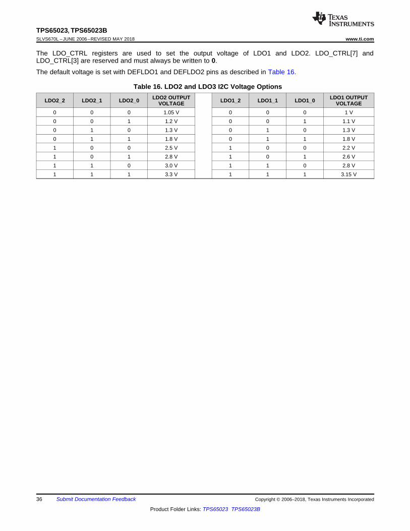
36
TPS65023, TPS65023BSLVS670L –JUNE 2006–REVISED MAY 2018 www.ti.com
Product Folder Links: TPS65023 TPS65023B
Submit Documentation Feedback Copyright © 2006–2018, Texas Instruments Incorporated
The LDO_CTRL registers are used to set the output voltage of LDO1 and LDO2. LDO_CTRL[7] andLDO_CTRL[3] are reserved and must always be written to 0.
The default voltage is set with DEFLDO1 and DEFLDO2 pins as described in Table 16.
Table 16. LDO2 and LDO3 I2C Voltage Options
LDO2_2 LDO2_1 LDO2_0 LDO2 OUTPUTVOLTAGE LDO1_2 LDO1_1 LDO1_0 LDO1 OUTPUT
VOLTAGE0 0 0 1.05 V 0 0 0 1 V0 0 1 1.2 V 0 0 1 1.1 V0 1 0 1.3 V 0 1 0 1.3 V0 1 1 1.8 V 0 1 1 1.8 V1 0 0 2.5 V 1 0 0 2.2 V1 0 1 2.8 V 1 0 1 2.6 V1 1 0 3.0 V 1 1 0 2.8 V1 1 1 3.3 V 1 1 1 3.15 V

VCC/VINDCDC1
DCDC1_EN
VDCDC1
1.225 V 1.225 V 1.225 V
37
TPS65023, TPS65023Bwww.ti.com SLVS670L –JUNE 2006–REVISED MAY 2018
Product Folder Links: TPS65023 TPS65023B
Submit Documentation FeedbackCopyright © 2006–2018, Texas Instruments Incorporated
8 Application and Implementation
NOTEInformation in the following applications sections is not part of the TI componentspecification, and TI does not warrant its accuracy or completeness. TI’s customers areresponsible for determining suitability of components for their purposes. Customers shouldvalidate and test their design implementation to confirm system functionality.
8.1 Application Information
8.1.1 Input Voltage ConnectionThe low power section of the control circuit for the step-down converters DCDC1, DCDC2, and DCDC3 issupplied by the VCC pin while the circuitry with high power such as the power stage is powered from theVINDCDC1, VINDCDC2, and VINDCDC3 pins. For proper operation of the step-down converters, VINDCDC1,VINDCDC2, VNDCDC3, and VCC must be tied to the same voltage rail. Step-down converters that are plannedto be not used, still need to be powered from their input pin on the same rails than the other step-downconverters and VCC.
LDO1 and LDO2 share a supply voltage pin which can be powered from the VCC rails or from a voltage lowerthan VCC, for example, the output of one of the step-down converters as long as it is operated within the inputvoltage range of the LDOs. If both LDOs are not used, the VINLDO pin can be tied to GND.
8.1.2 Unused RegulatorsIn case a step-down converter is not used, its input supply voltage pin VINDCDCx still needs to be connected tothe VCC rail along with supply input of the other step-down converters. TI recommends closing the control loopsuch that an inductor and output capacitor is added in the same way as it would be when operated normally. Ifone of the LDOs is not used, its output capacitor must be added as well. If both LDOs are not used, the inputsupply pin as well as the output pins of the LDOs (VINLDO, VLDO1, VLDO2) must be tied to GND.
8.1.3 Reset Condition of DCDC1If DEFDCDC1 is connected to ground and DCDC1_EN is pulled high after VINDCDC1 is applied, the outputvoltage of DCDC1 defaults to 1.225 V instead of 1.2 V (high by 2%). Figure 36 illustrates the problem.
Figure 36. Default DCDC1

VCC/VINDCDC1
DCDC1_EN
HOT_RESET
VDCDC1
1.225 V1.20 V1.225 V
1.20 V
VCC/VINDCDC1
DCDC1_EN
I2C Bus
DEF_CORE
VDCDC1
?? 0x1F 0x11 0x10 ?? 0x1E0x1F 0x10
1.20 V1.225 V
1.20 V
Pull DCDC1_EN HighWrite DEF_CORE to 0x10Write CON_CTRL [7] to 1
Write DEF_CORE to 0x10Pull DCDC1_EN High
VCC/VINDCDC1
DCDC1_EN
VDCDC1
1.20 V 1.20 V 1.20 V
38
TPS65023, TPS65023BSLVS670L –JUNE 2006–REVISED MAY 2018 www.ti.com
Product Folder Links: TPS65023 TPS65023B
Submit Documentation Feedback Copyright © 2006–2018, Texas Instruments Incorporated
Application Information (continued)One workaround is to tie DCDC1_EN to VINDCDC1 (Figure 37).
Figure 37. Workaround 1
Another workaround is to write the correct voltage to the DEF_CORE register through I2C. This can be donebefore or after the converter is enabled. If written before the enable, the only bit changed is DEF_CORE[0]. Thevoltage is 1.2 V, however, when the enable is pulled high (Figure 38).
Figure 38. Workaround 2
A third workaround is to generate a HOT_RESET after enabling DCDC1 (Figure 39)
Figure 39. Workaround 3

39
TPS65023, TPS65023Bwww.ti.com SLVS670L –JUNE 2006–REVISED MAY 2018
Product Folder Links: TPS65023 TPS65023B
Submit Documentation FeedbackCopyright © 2006–2018, Texas Instruments Incorporated
Application Information (continued)Table 17. Changes of TPS65023B vs TPS65023
ITEM DESCRIPTION Reference TPS65023 TPS65023B
VIH High level input voltage for the SDAT pin
ElectricalCharacteristics
Minimum 1.3 V
Minimum 1.69 V;Vcc = 2.5 V to 5.25 V
Minimum 1.55 V;Vcc = 2.5 V to 4.5 V
VIH High level input voltage for the SCLK pin Minimum 1.3 V Minimum 1.4 V;Vcc = 2.5 V to 5.25 V
VILLow level input voltage for SCLK andSDAT pin Maximum 0.4 V Maximum 0.35 V
th(DATA) Data input hold time I2C TimingRequirements for
TPS65023B
Minimum 300 ns Minimum 100 ns
tsu(DATA) Data input setup time Minimum 300 ns Minimum 100 ns
8.2 Typical Application
Figure 40. Typical Configuration for the Texas Instruments TMS320DM644x DaVinci™ Processors
8.2.1 Design RequirementsThe TPS6502x devices have only a few design requirements. Use the following parameters for the designexamples:• 1- μ F bypass capacitor on VCC, located as close as possible to the VCC pin to ground• VCC and VINDCDCx must be connected to the same voltage supply with minimal voltage difference.• Input capacitors must be present on the VINDCDCx and VIN_LDO supplies if used• Output inductor and capacitors must be used on the outputs of the DC–DC converters if used• Output capacitors must be used on the outputs of the LDOs if used

LLmax outmax
II I
2
'
L
Vout1
VinI Vout/ ¦
' uu
40
TPS65023, TPS65023BSLVS670L –JUNE 2006–REVISED MAY 2018 www.ti.com
Product Folder Links: TPS65023 TPS65023B
Submit Documentation Feedback Copyright © 2006–2018, Texas Instruments Incorporated
Typical Application (continued)8.2.2 Detailed Design Procedure
8.2.2.1 Inductor Selection for the DC-DC ConvertersEach of the converters in the TPS65023x typically use a 2.2-μH output inductor. Larger or smaller inductorvalues are used to optimize the performance of the device for specific operation conditions. The selectedinductor has to be rated for its DC resistance and saturation current. The DC resistance of the inductanceinfluences directly the efficiency of the converter. Therefore, an inductor with lowest DC resistance must beselected for highest efficiency.
For a fast transient response, a 2.2-μH inductor in combination with a 22-μF output capacitor is recommended.
Equation 8 calculates the maximum inductor current under static load conditions. The saturation current of theinductor must be rated higher than the maximum inductor current as calculated with Equation 8. This is neededbecause during heavy load transient the inductor current rises above the calculated value.
(8)
where• f = Switching Frequency (2.25 MHz typical)• L = Inductor Value• ΔIL = Peak-to-Peak inductor ripple current• ILMAX = Maximum Inductor current (9)
The highest inductor current occurs at maximum Vin.
Open-core inductors have a soft saturation characteristic, and they can usually handle higher inductor currentsversus a comparable shielded inductor.
A conservative approach is to select the inductor current rating just for the maximum switch current of theTPS65023x (2 A for the VDCDC1 and VDCDC2 converters, and 1.5 A for the VDCDC3 converter). The corematerial from inductor to inductor differs and has an impact on the efficiency especially at high switchingfrequencies.
See Table 18 and the typical applications for possible inductors.
Table 18. Tested Inductors
DEVICE INDUCTORVALUE TYPE COMPONENT SUPPLIER
All converters2.2 μH LPS4012-222LMB Coilcraft2.2 μH VLCF4020T-2R2N1R7 TDK
For DCDC2 orDCDC3
2.2 uH LQH32PN2R2NN0 Murata
For DCDC1 1.5 uH LQH32PN1R5NN0 MurataAll converters 2.2 uH PST25201B-2R2MS Cyntec
8.2.2.2 Output Capacitor SelectionThe advanced fast response voltage mode control scheme of the inductive converters implemented in theTPS65023x allow the use of small ceramic capacitors with a typical value of 10 μF for each converter withouthaving large output voltage under and overshoots during heavy load transients. Ceramic capacitors having lowESR values have the lowest output voltage ripple and are recommended. See Table 19 for recommendedcomponents.

DVout = Vout x
1 -Vout
Vin
L x ¦x + ESR( )1
8 x C xout ¦
IRMSCout
= Vout
x
1 -V
out
Vin
L x ¦x
1
2 x 3Ö
41
TPS65023, TPS65023Bwww.ti.com SLVS670L –JUNE 2006–REVISED MAY 2018
Product Folder Links: TPS65023 TPS65023B
Submit Documentation FeedbackCopyright © 2006–2018, Texas Instruments Incorporated
If ceramic output capacitors are used, the capacitor RMS ripple current rating always meets the applicationrequirements. Just for completeness, the RMS ripple current is calculated in Equation 10.
(10)
At nominal load current, the inductive converters operate in PWM mode. The overall output voltage ripple is thesum of the voltage spike caused by the output capacitor ESR plus the voltage ripple caused by charging anddischarging the output capacitor:
where• The highest output voltage ripple occurs at the highest input voltage Vin (11)
At light load currents, the converters operate in PSM and the output voltage ripple is dependent on the outputcapacitor value. The output voltage ripple is set by the internal comparator delay and the external capacitor. Thetypical output voltage ripple is less than 1% of the nominal output voltage.
8.2.2.3 Input Capacitor SelectionBecause of the nature of the buck converter having a pulsating input current, a low ESR input capacitor isrequired for best input voltage filtering and minimizing the interference with other circuits caused by high inputvoltage spikes. Each DC-DC converter requires a 10-μF ceramic input capacitor on its input pin VINDCDCx. Theinput capacitor is increased without any limit for better input voltage filtering. The VCC pin is separated from theinput for the DC-DC converters. A filter resistor of up to 10R and a 1-μF capacitor is used for decoupling the VCCpin from switching noise. Note that the filter resistor may affect the UVLO threshold since up to 3 mA can flowthrough this resistor into the VCC pin when all converters are running in PWM mode.
Table 19. Possible CapacitorsCAPACITOR VALUE CASE SIZE COMPONENT SUPPLIER COMMENTS
22 μF 1206 TDK C3216X5R0J226M Ceramic22 μF 1206 Taiyo Yuden JMK316BJ226ML Ceramic22 μF 0805 TDK C2012X5R0J226MT Ceramic22 μF 0805 Taiyo Yuden JMK212BJ226MG Ceramic10 μF 0805 Taiyo Yuden JMK212BJ106M Ceramic10 μF 0805 TDK C2012X5R0J106M Ceramic
8.2.2.4 Output Voltage SelectionThe DEFDCDC1, DEFDCDC2, and DEFDCDC3 pins are used to set the output voltage for each step-downconverter. See Table 20 for the default voltages if the pins are pulled to GND or to VCC. If a different voltage isneeded, an external resistor divider can be added to the DEFDCDCx pin as shown in Figure 41.
The output voltage of VDCDC1 is set with the I2C interface. If the voltage is changed from the default, using theDEFCORE register, the output voltage only depends on the register value. Any resistor divider at DEFDCDC1does not change the voltage set with the register.
Table 20. DCDC1, DCDC2, and DCDC3 Default Voltage LevelsPIN LEVEL DEFAULT OUTPUT VOLTAGE
DEFDCDC1VCC 1.6 VGND 1.2 V
DEFDCDC2VCC 3.3 VGND 1.8 V
t = 2(reset) x 128 x(1 V - 0.25 V) x C(reset)
2 Am( )
VOUT DEFDCDCx= V x R1 + R2
R2R1 = R2 x
VOUT
VDEFDCDCx
- R2( )
VDCDC3
DCDC3_EN DEFDCDC3
AGND PGND
L3
R1
R2
VOL
CO
VCC
VINDCDC3
CI
1 Fm
10 RV(bat)
42
TPS65023, TPS65023BSLVS670L –JUNE 2006–REVISED MAY 2018 www.ti.com
Product Folder Links: TPS65023 TPS65023B
Submit Documentation Feedback Copyright © 2006–2018, Texas Instruments Incorporated
Table 20. DCDC1, DCDC2, and DCDC3 Default Voltage Levels (continued)PIN LEVEL DEFAULT OUTPUT VOLTAGE
DEFDCDC3VCC 3.3 VGND 1.8 V
Using an external resistor divider at DEFDCDCx:
Figure 41. External Resistor Divider
When a resistor divider is connected to DEFDCDCx, the output voltage can be set from 0.6 V up to the inputvoltage V(bat). The total resistance (R1 + R2) of the voltage divider must be kept in the 1-MR range to maintain ahigh efficiency at light load.
V(DEFDCDCx) = 0.6 V
(12)
8.2.2.5 VRTC OutputIt is required that a 4.7-μF (minimum) capacitor be added to the VRTC pin even if the output is not used.
8.2.2.6 LDO1 and LDO2The LDOs in the TPS65023x are general-purpose LDOs which are stable using ceramics capacitors. Theminimum output capacitor required is 2.2 μF. The LDOs output voltage can be changed to different voltagesbetween 1 V and 3.3 V using the I2C interface. Therefore, they can also be used as general-purpose LDOs inapplications powering processors different from DaVinci. The supply voltage for the LDOs needs to be connectedto the VINLDO pin, giving the flexibility to connect the lowest voltage available in the system and provides thehighest efficiency.
8.2.2.7 TRESPWRONThis is the input to a capacitor that defines the reset delay time after the voltage at VRTC rises above 2.52 V.The timing is generated by charging and discharging the capacitor with a current of 2 μA between a threshold of0.25 V and 1 V for 128 cycles. A 1-nF capacitor gives a delay time of 100 ms.
While there is no real upper and lower limit for the capacitor connected to TRESPWRON, TI recommends notleaving signal pins open.
where

0
10
20
30
40
50
60
70
80
90
100
0.01 0.1 1 10 100 1 k 10 k
I - Output Current - mAO
Eff
icie
ncy -
%
T = 25°C
V = 1.2 V
PWM/PFM Mode
A
O
V = 4.2 VI
V = 2.5 VI
V = 3.6 VI
V = 5 VI
0
10
20
30
40
50
60
70
80
90
100
0.01 0.1 1 10 100 1 k 10 k
I - Output Current - mAO
Eff
icie
ncy -
%
T = 25°C
V = 1.8 V
PWM/PFM Mode
A
O
V = 4.2 VI
V = 2.5 VI
V = 3.6 VI
V = 5 VI
43
TPS65023, TPS65023Bwww.ti.com SLVS670L –JUNE 2006–REVISED MAY 2018
Product Folder Links: TPS65023 TPS65023B
Submit Documentation FeedbackCopyright © 2006–2018, Texas Instruments Incorporated
• t(reset) is the reset delay time• C(reset) is the capacitor connected to the TRESPWRON pin (13)
The minimum and maximum values for the timing parameters called ICONST (2 uA), TRESPWRON_UPTH (1V), and TRESPWRON_LOWTH (0.25 V) can be found under Electrical Characteristics.
8.2.2.8 VCC FilterAn RC filter connected at the VCC input is used to keep noise from the internal supply for the bandgap and otheranalog circuitry. A typical value of 1 R and 1 μF is used to filter the switching spikes, generated by the DC-DCconverters. A larger resistor than 10 R must not be used because the current into VCC of up to 3 mA causes avoltage drop at the resistor causing the undervoltage lockout circuitry connected at VCC internally to switch offtoo early.
8.2.3 Application CurvesGraphs were taken using the EVM with the following inductor and output capacitor combinations:
CONVERTER INDUCTOR OUTPUT CAPACITOR OUTPUT CAPACITOR VALUEVDCDC1 VLCF4020-2R2 C2012X5R0J106M 2 × 10 μFVDCDC2 VLCF4020-2R2 C2012X5R0J106M 2 × 10 μFVDCDC3 VLF4012AT-2R2M1R5 C2012X5R0J106M 2 × 10 μF
Figure 42. DCDC1 Efficiency Figure 43. DCDC2 Efficiency
0
10
20
30
40
50
60
70
80
90
100
0.01 0.1 1 10 100 1 k 10 k
I - Output Current - mAO
Eff
icie
ncy -
%
T = 25°C
V = 1.8 V
PWM/PFM Mode
A
O
V = 4.2 VI
V = 2.5 VI
V = 3.6 VI
V = 5 VI
44
TPS65023, TPS65023BSLVS670L –JUNE 2006–REVISED MAY 2018 www.ti.com
Product Folder Links: TPS65023 TPS65023B
Submit Documentation Feedback Copyright © 2006–2018, Texas Instruments Incorporated
Figure 44. DCDC3 Efficiency
9 Power Supply Recommendations
9.1 Requirements for Supply Voltages Below 3.0 VFor a supply voltage on pins Vcc, VINDCDC1, VINDCDC2, and VINDCDC3 below 3.0 V, TI recommendsenabling the DCDC1, DCDC2, and DCDC3 converters in sequence. If all 3 step-down converters are enabled atthe same time while the supply voltage is close to the internal reset detection threshold, a reset may begenerated during power-up. Therefore TI recommends enabling the DC-DC converters in sequence. This can bedone by driving one or two of the enable pins with a RC delay or by driving the enable pin by the output voltageof one of the other step-down converters. If a voltage above 3.0 V is applied on pin VBACKUP while VCC andVINDCDCx is below 3.0 V, there is no restriction in the power-up sequencing as VBACKUP will be used to powerthe internal circuitry.
CIN L3
Cout
Cout
PGND3
VDCDC3
VIN
45
TPS65023, TPS65023Bwww.ti.com SLVS670L –JUNE 2006–REVISED MAY 2018
Product Folder Links: TPS65023 TPS65023B
Submit Documentation FeedbackCopyright © 2006–2018, Texas Instruments Incorporated
10 Layout
10.1 Layout GuidelinesAs for all switching power supplies, the layout is an important step in the design. Proper function of the devicedemands careful attention to PCB layout. Take care in board layout to get the specified performance. If thelayout is not carefully done, the regulators may show poor line, load regulation, or both, along with stability issuesand EMI problems. It is critical to provide a low impedance ground path. Therefore, use wide and short traces forthe main current paths. The input capacitors must be placed as close as possible to the IC pins as well as theinductor and output capacitor.
For TPS65023x, connect the PGND pins of the device to the thermal pad land of the PCB and connect theanalog ground connections (AGND) to the PGND at the thermal pad. It is essential to provide a good thermaland electrical connection of all GND pins using multiple vias to the GND-plane. Keep the common path to theAGND pins, which returns the small signal components, and the high current of the output capacitors as short aspossible to avoid ground noise. The VDCDCx line must be connected right to the output capacitor and routedaway from noisy components and traces (for example, the L1, L2, and L3 traces).
10.2 Layout Example
Figure 45. Layout Example of a DC–DC Converter
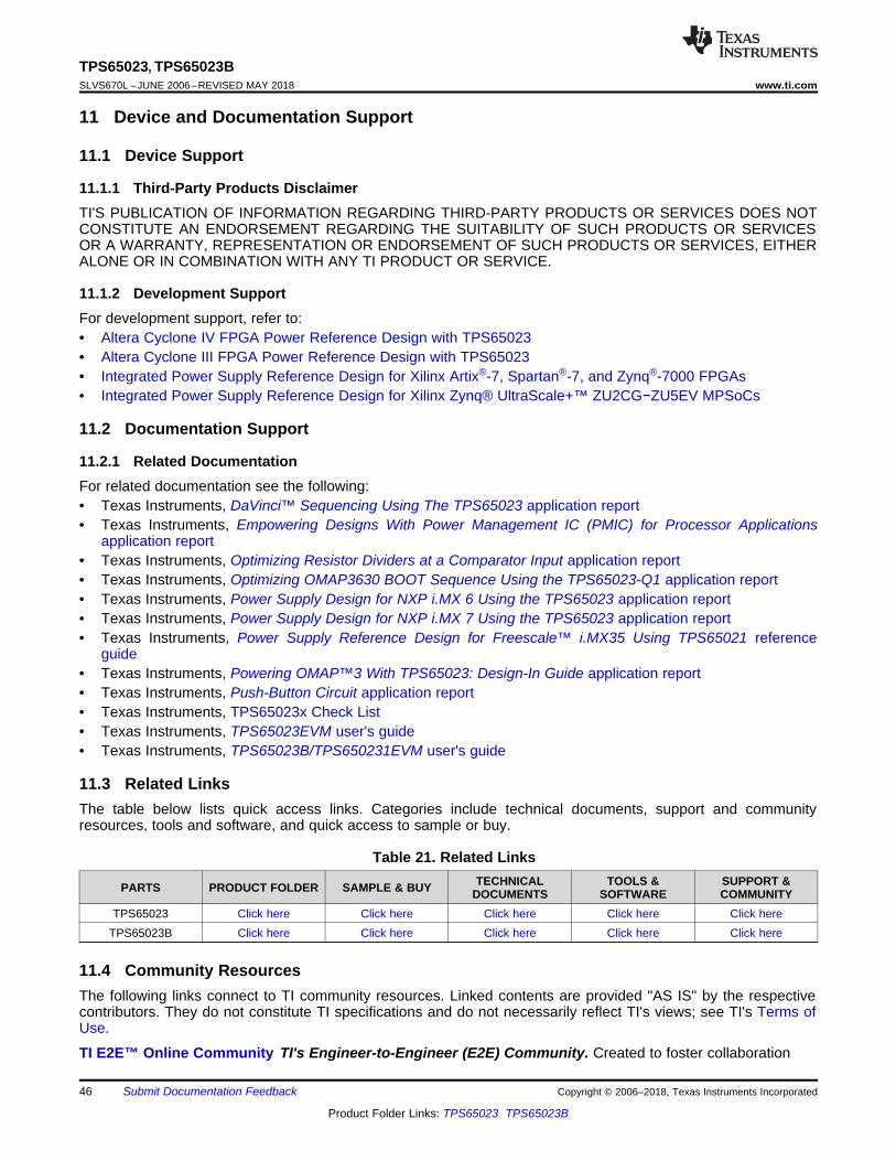
46
TPS65023, TPS65023BSLVS670L –JUNE 2006–REVISED MAY 2018 www.ti.com
Product Folder Links: TPS65023 TPS65023B
Submit Documentation Feedback Copyright © 2006–2018, Texas Instruments Incorporated
11 Device and Documentation Support
11.1 Device Support
11.1.1 Third-Party Products DisclaimerTI'S PUBLICATION OF INFORMATION REGARDING THIRD-PARTY PRODUCTS OR SERVICES DOES NOTCONSTITUTE AN ENDORSEMENT REGARDING THE SUITABILITY OF SUCH PRODUCTS OR SERVICESOR A WARRANTY, REPRESENTATION OR ENDORSEMENT OF SUCH PRODUCTS OR SERVICES, EITHERALONE OR IN COMBINATION WITH ANY TI PRODUCT OR SERVICE.
11.1.2 Development SupportFor development support, refer to:• Altera Cyclone IV FPGA Power Reference Design with TPS65023• Altera Cyclone III FPGA Power Reference Design with TPS65023• Integrated Power Supply Reference Design for Xilinx Artix®-7, Spartan®-7, and Zynq®-7000 FPGAs• Integrated Power Supply Reference Design for Xilinx Zynq® UltraScale+™ ZU2CG−ZU5EV MPSoCs
11.2 Documentation Support
11.2.1 Related DocumentationFor related documentation see the following:• Texas Instruments, DaVinci™ Sequencing Using The TPS65023 application report• Texas Instruments, Empowering Designs With Power Management IC (PMIC) for Processor Applications
application report• Texas Instruments, Optimizing Resistor Dividers at a Comparator Input application report• Texas Instruments, Optimizing OMAP3630 BOOT Sequence Using the TPS65023-Q1 application report• Texas Instruments, Power Supply Design for NXP i.MX 6 Using the TPS65023 application report• Texas Instruments, Power Supply Design for NXP i.MX 7 Using the TPS65023 application report• Texas Instruments, Power Supply Reference Design for Freescale™ i.MX35 Using TPS65021 reference
guide• Texas Instruments, Powering OMAP™3 With TPS65023: Design-In Guide application report• Texas Instruments, Push-Button Circuit application report• Texas Instruments, TPS65023x Check List• Texas Instruments, TPS65023EVM user's guide• Texas Instruments, TPS65023B/TPS650231EVM user's guide
11.3 Related LinksThe table below lists quick access links. Categories include technical documents, support and communityresources, tools and software, and quick access to sample or buy.
Table 21. Related Links
PARTS PRODUCT FOLDER SAMPLE & BUY TECHNICALDOCUMENTS
TOOLS &SOFTWARE
SUPPORT &COMMUNITY
TPS65023 Click here Click here Click here Click here Click hereTPS65023B Click here Click here Click here Click here Click here
11.4 Community ResourcesThe following links connect to TI community resources. Linked contents are provided "AS IS" by the respectivecontributors. They do not constitute TI specifications and do not necessarily reflect TI's views; see TI's Terms ofUse.
TI E2E™ Online Community TI's Engineer-to-Engineer (E2E) Community. Created to foster collaboration

47
TPS65023, TPS65023Bwww.ti.com SLVS670L –JUNE 2006–REVISED MAY 2018
Product Folder Links: TPS65023 TPS65023B
Submit Documentation FeedbackCopyright © 2006–2018, Texas Instruments Incorporated
Community Resources (continued)among engineers. At e2e.ti.com, you can ask questions, share knowledge, explore ideas and helpsolve problems with fellow engineers.
Design Support TI's Design Support Quickly find helpful E2E forums along with design support tools andcontact information for technical support.
11.5 TrademarksDaVinci, OMAP, E2E are trademarks of Texas Instruments.Freescale is a trademark of Motorola, Inc.I2C is a trademark of NXP Semiconductors.UltraScale+ is a trademark of Xilinx Inc.Artix, Spartan, Zynq are registered trademarks of Xilinx Inc.All other trademarks are the property of their respective owners.
11.6 Electrostatic Discharge CautionThis integrated circuit can be damaged by ESD. Texas Instruments recommends that all integrated circuits be handled withappropriate precautions. Failure to observe proper handling and installation procedures can cause damage.
ESD damage can range from subtle performance degradation to complete device failure. Precision integrated circuits may be moresusceptible to damage because very small parametric changes could cause the device not to meet its published specifications.
11.7 GlossarySLYZ022 — TI Glossary.
This glossary lists and explains terms, acronyms, and definitions.
12 Mechanical, Packaging, and Orderable InformationThe following pages include mechanical, packaging, and orderable information. This information is the mostcurrent data available for the designated devices. This data is subject to change without notice and revision ofthis document. For browser-based versions of this data sheet, refer to the left-hand navigation.
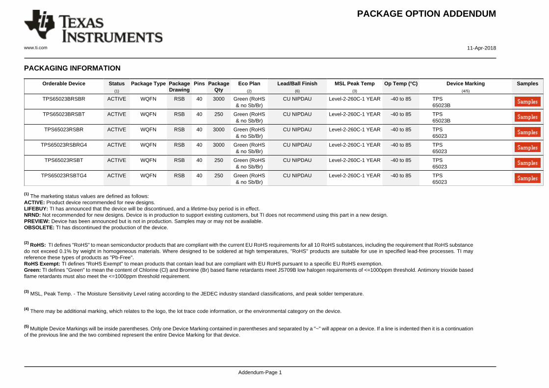
PACKAGE OPTION ADDENDUM
www.ti.com 11-Apr-2018
Addendum-Page 1
PACKAGING INFORMATION
Orderable Device Status(1)
Package Type PackageDrawing
Pins PackageQty
Eco Plan(2)
Lead/Ball Finish(6)
MSL Peak Temp(3)
Op Temp (°C) Device Marking(4/5)
Samples
TPS65023BRSBR ACTIVE WQFN RSB 40 3000 Green (RoHS& no Sb/Br)
CU NIPDAU Level-2-260C-1 YEAR -40 to 85 TPS65023B
TPS65023BRSBT ACTIVE WQFN RSB 40 250 Green (RoHS& no Sb/Br)
CU NIPDAU Level-2-260C-1 YEAR -40 to 85 TPS65023B
TPS65023RSBR ACTIVE WQFN RSB 40 3000 Green (RoHS& no Sb/Br)
CU NIPDAU Level-2-260C-1 YEAR -40 to 85 TPS65023
TPS65023RSBRG4 ACTIVE WQFN RSB 40 3000 Green (RoHS& no Sb/Br)
CU NIPDAU Level-2-260C-1 YEAR -40 to 85 TPS65023
TPS65023RSBT ACTIVE WQFN RSB 40 250 Green (RoHS& no Sb/Br)
CU NIPDAU Level-2-260C-1 YEAR -40 to 85 TPS65023
TPS65023RSBTG4 ACTIVE WQFN RSB 40 250 Green (RoHS& no Sb/Br)
CU NIPDAU Level-2-260C-1 YEAR -40 to 85 TPS65023
(1) The marketing status values are defined as follows:ACTIVE: Product device recommended for new designs.LIFEBUY: TI has announced that the device will be discontinued, and a lifetime-buy period is in effect.NRND: Not recommended for new designs. Device is in production to support existing customers, but TI does not recommend using this part in a new design.PREVIEW: Device has been announced but is not in production. Samples may or may not be available.OBSOLETE: TI has discontinued the production of the device.
(2) RoHS: TI defines "RoHS" to mean semiconductor products that are compliant with the current EU RoHS requirements for all 10 RoHS substances, including the requirement that RoHS substancedo not exceed 0.1% by weight in homogeneous materials. Where designed to be soldered at high temperatures, "RoHS" products are suitable for use in specified lead-free processes. TI mayreference these types of products as "Pb-Free".RoHS Exempt: TI defines "RoHS Exempt" to mean products that contain lead but are compliant with EU RoHS pursuant to a specific EU RoHS exemption.Green: TI defines "Green" to mean the content of Chlorine (Cl) and Bromine (Br) based flame retardants meet JS709B low halogen requirements of <=1000ppm threshold. Antimony trioxide basedflame retardants must also meet the <=1000ppm threshold requirement.
(3) MSL, Peak Temp. - The Moisture Sensitivity Level rating according to the JEDEC industry standard classifications, and peak solder temperature.
(4) There may be additional marking, which relates to the logo, the lot trace code information, or the environmental category on the device.
(5) Multiple Device Markings will be inside parentheses. Only one Device Marking contained in parentheses and separated by a "~" will appear on a device. If a line is indented then it is a continuationof the previous line and the two combined represent the entire Device Marking for that device.

PACKAGE OPTION ADDENDUM
www.ti.com 11-Apr-2018
Addendum-Page 2
(6) Lead/Ball Finish - Orderable Devices may have multiple material finish options. Finish options are separated by a vertical ruled line. Lead/Ball Finish values may wrap to two lines if the finishvalue exceeds the maximum column width.
Important Information and Disclaimer:The information provided on this page represents TI's knowledge and belief as of the date that it is provided. TI bases its knowledge and belief on informationprovided by third parties, and makes no representation or warranty as to the accuracy of such information. Efforts are underway to better integrate information from third parties. TI has taken andcontinues to take reasonable steps to provide representative and accurate information but may not have conducted destructive testing or chemical analysis on incoming materials and chemicals.TI and TI suppliers consider certain information to be proprietary, and thus CAS numbers and other limited information may not be available for release.
In no event shall TI's liability arising out of such information exceed the total purchase price of the TI part(s) at issue in this document sold by TI to Customer on an annual basis.
OTHER QUALIFIED VERSIONS OF TPS65023 :
• Automotive: TPS65023-Q1
NOTE: Qualified Version Definitions:
• Automotive - Q100 devices qualified for high-reliability automotive applications targeting zero defects
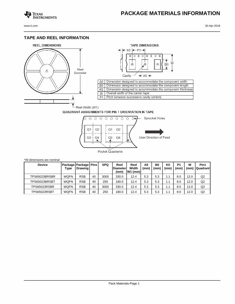
TAPE AND REEL INFORMATION
*All dimensions are nominal
Device PackageType
PackageDrawing
Pins SPQ ReelDiameter
(mm)
ReelWidth
W1 (mm)
A0(mm)
B0(mm)
K0(mm)
P1(mm)
W(mm)
Pin1Quadrant
TPS65023BRSBR WQFN RSB 40 3000 330.0 12.4 5.3 5.3 1.1 8.0 12.0 Q2
TPS65023BRSBT WQFN RSB 40 250 180.0 12.4 5.3 5.3 1.1 8.0 12.0 Q2
TPS65023RSBR WQFN RSB 40 3000 330.0 12.4 5.3 5.3 1.1 8.0 12.0 Q2
TPS65023RSBT WQFN RSB 40 250 180.0 12.4 5.3 5.3 1.1 8.0 12.0 Q2
PACKAGE MATERIALS INFORMATION
www.ti.com 30-Apr-2018
Pack Materials-Page 1
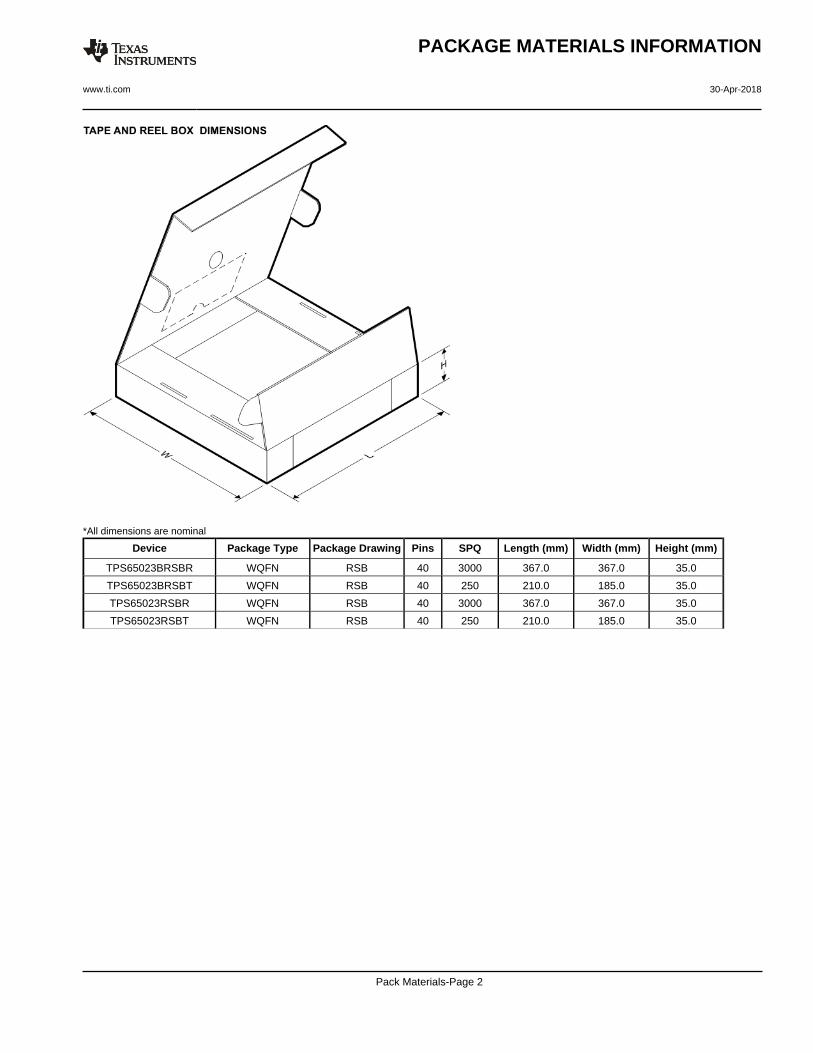
*All dimensions are nominal
Device Package Type Package Drawing Pins SPQ Length (mm) Width (mm) Height (mm)
TPS65023BRSBR WQFN RSB 40 3000 367.0 367.0 35.0
TPS65023BRSBT WQFN RSB 40 250 210.0 185.0 35.0
TPS65023RSBR WQFN RSB 40 3000 367.0 367.0 35.0
TPS65023RSBT WQFN RSB 40 250 210.0 185.0 35.0
PACKAGE MATERIALS INFORMATION
www.ti.com 30-Apr-2018
Pack Materials-Page 2


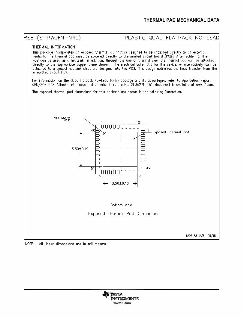


IMPORTANT NOTICE
Texas Instruments Incorporated (TI) reserves the right to make corrections, enhancements, improvements and other changes to itssemiconductor products and services per JESD46, latest issue, and to discontinue any product or service per JESD48, latest issue. Buyersshould obtain the latest relevant information before placing orders and should verify that such information is current and complete.TI’s published terms of sale for semiconductor products (http://www.ti.com/sc/docs/stdterms.htm) apply to the sale of packaged integratedcircuit products that TI has qualified and released to market. Additional terms may apply to the use or sale of other types of TI products andservices.Reproduction of significant portions of TI information in TI data sheets is permissible only if reproduction is without alteration and isaccompanied by all associated warranties, conditions, limitations, and notices. TI is not responsible or liable for such reproduceddocumentation. Information of third parties may be subject to additional restrictions. Resale of TI products or services with statementsdifferent from or beyond the parameters stated by TI for that product or service voids all express and any implied warranties for theassociated TI product or service and is an unfair and deceptive business practice. TI is not responsible or liable for any such statements.Buyers and others who are developing systems that incorporate TI products (collectively, “Designers”) understand and agree that Designersremain responsible for using their independent analysis, evaluation and judgment in designing their applications and that Designers havefull and exclusive responsibility to assure the safety of Designers' applications and compliance of their applications (and of all TI productsused in or for Designers’ applications) with all applicable regulations, laws and other applicable requirements. Designer represents that, withrespect to their applications, Designer has all the necessary expertise to create and implement safeguards that (1) anticipate dangerousconsequences of failures, (2) monitor failures and their consequences, and (3) lessen the likelihood of failures that might cause harm andtake appropriate actions. Designer agrees that prior to using or distributing any applications that include TI products, Designer willthoroughly test such applications and the functionality of such TI products as used in such applications.TI’s provision of technical, application or other design advice, quality characterization, reliability data or other services or information,including, but not limited to, reference designs and materials relating to evaluation modules, (collectively, “TI Resources”) are intended toassist designers who are developing applications that incorporate TI products; by downloading, accessing or using TI Resources in anyway, Designer (individually or, if Designer is acting on behalf of a company, Designer’s company) agrees to use any particular TI Resourcesolely for this purpose and subject to the terms of this Notice.TI’s provision of TI Resources does not expand or otherwise alter TI’s applicable published warranties or warranty disclaimers for TIproducts, and no additional obligations or liabilities arise from TI providing such TI Resources. TI reserves the right to make corrections,enhancements, improvements and other changes to its TI Resources. TI has not conducted any testing other than that specificallydescribed in the published documentation for a particular TI Resource.Designer is authorized to use, copy and modify any individual TI Resource only in connection with the development of applications thatinclude the TI product(s) identified in such TI Resource. NO OTHER LICENSE, EXPRESS OR IMPLIED, BY ESTOPPEL OR OTHERWISETO ANY OTHER TI INTELLECTUAL PROPERTY RIGHT, AND NO LICENSE TO ANY TECHNOLOGY OR INTELLECTUAL PROPERTYRIGHT OF TI OR ANY THIRD PARTY IS GRANTED HEREIN, including but not limited to any patent right, copyright, mask work right, orother intellectual property right relating to any combination, machine, or process in which TI products or services are used. Informationregarding or referencing third-party products or services does not constitute a license to use such products or services, or a warranty orendorsement thereof. Use of TI Resources may require a license from a third party under the patents or other intellectual property of thethird party, or a license from TI under the patents or other intellectual property of TI.TI RESOURCES ARE PROVIDED “AS IS” AND WITH ALL FAULTS. TI DISCLAIMS ALL OTHER WARRANTIES ORREPRESENTATIONS, EXPRESS OR IMPLIED, REGARDING RESOURCES OR USE THEREOF, INCLUDING BUT NOT LIMITED TOACCURACY OR COMPLETENESS, TITLE, ANY EPIDEMIC FAILURE WARRANTY AND ANY IMPLIED WARRANTIES OFMERCHANTABILITY, FITNESS FOR A PARTICULAR PURPOSE, AND NON-INFRINGEMENT OF ANY THIRD PARTY INTELLECTUALPROPERTY RIGHTS. TI SHALL NOT BE LIABLE FOR AND SHALL NOT DEFEND OR INDEMNIFY DESIGNER AGAINST ANY CLAIM,INCLUDING BUT NOT LIMITED TO ANY INFRINGEMENT CLAIM THAT RELATES TO OR IS BASED ON ANY COMBINATION OFPRODUCTS EVEN IF DESCRIBED IN TI RESOURCES OR OTHERWISE. IN NO EVENT SHALL TI BE LIABLE FOR ANY ACTUAL,DIRECT, SPECIAL, COLLATERAL, INDIRECT, PUNITIVE, INCIDENTAL, CONSEQUENTIAL OR EXEMPLARY DAMAGES INCONNECTION WITH OR ARISING OUT OF TI RESOURCES OR USE THEREOF, AND REGARDLESS OF WHETHER TI HAS BEENADVISED OF THE POSSIBILITY OF SUCH DAMAGES.Unless TI has explicitly designated an individual product as meeting the requirements of a particular industry standard (e.g., ISO/TS 16949and ISO 26262), TI is not responsible for any failure to meet such industry standard requirements.Where TI specifically promotes products as facilitating functional safety or as compliant with industry functional safety standards, suchproducts are intended to help enable customers to design and create their own applications that meet applicable functional safety standardsand requirements. Using products in an application does not by itself establish any safety features in the application. Designers mustensure compliance with safety-related requirements and standards applicable to their applications. Designer may not use any TI products inlife-critical medical equipment unless authorized officers of the parties have executed a special contract specifically governing such use.Life-critical medical equipment is medical equipment where failure of such equipment would cause serious bodily injury or death (e.g., lifesupport, pacemakers, defibrillators, heart pumps, neurostimulators, and implantables). Such equipment includes, without limitation, allmedical devices identified by the U.S. Food and Drug Administration as Class III devices and equivalent classifications outside the U.S.TI may expressly designate certain products as completing a particular qualification (e.g., Q100, Military Grade, or Enhanced Product).Designers agree that it has the necessary expertise to select the product with the appropriate qualification designation for their applicationsand that proper product selection is at Designers’ own risk. Designers are solely responsible for compliance with all legal and regulatoryrequirements in connection with such selection.Designer will fully indemnify TI and its representatives against any damages, costs, losses, and/or liabilities arising out of Designer’s non-compliance with the terms and provisions of this Notice.
Mailing Address: Texas Instruments, Post Office Box 655303, Dallas, Texas 75265Copyright © 2018, Texas Instruments Incorporated