d10 assembling of bs frontend - eth zürich · d10 – assembling of bs frontend page 4 resolution...
TRANSCRIPT

RESOLUTION Reconfigurable Systems for Mobile Local Communication and Positioning
RESOLUTION Project IST - 026851 Assembling of BS Frontend [D10]
Document Information
Title D10 – Assembling of BS Frontend
Workpackage WP4 – CMOS systems
Responsible TUD
Due Date Project Month 18 (July 2007)
Type Prototype
Status Version 1.0
Security Public
Authors Marko Krcmar, Viswanathan Subramanian, Thomas Ußmüller, Jörg Carls
Project URL http://www.ife.ee.ethz.ch/RESOLUTION/
D10 – Assembling of BS Frontend Page 2
RESOLUTION 2007-07-30
Table of contents 1 INTRODUCTION ............................................................................................. 3
2 OVERVIEW OF RF FRONTEND ARCHITECTURE ............................................... 3
3 SYNTHESISER ARCHITECTURE ....................................................................... 3
3.1 PHASE-FREQUENCY DETECTOR ............................................................................ 5
3.2 CHARGE-PUMP ................................................................................................ 5
3.3 LOOP FILTER .................................................................................................. 6
3.4 MMD ARCHITECTURE ....................................................................................... 6
3.5 VCO ARCHITECTURE ........................................................................................ 7
4 TRANSMITTER ARCHITECTURE ...................................................................... 8
4.1 PA ARCHITECTURES ......................................................................................... 8
4.2 CHARACTERISATION OF CLASS A PA ................................................................... 9
4.3 CHARACTERISATION OF CLASS F PA .................................................................. 11
4.4 REALIZATION PRINTED WIRE BOARDS ................................................................ 12
4.5 CLASS A BASED TRANSMITTER SUBSYSTEM WITH DC SWITCH .................................. 13
4.6 CLASS F BASED TRANSMITTER SUBSYSTEM WITHOUT DC SWITCH ............................. 15
5 RECEIVER ARCHITECTURE ........................................................................... 16
5.1 INTRODUCTION ............................................................................................. 16
5.2 RECEIVER CORE ............................................................................................ 16
6 INTEGRATION OF VCO WITH RECEIVER ...................................................... 19
7 INTEGRATION OF VCO WITH TRANSMITTER ................................................ 22
7.1 MEASUREMENT SETUP .................................................................................... 22
7.2 MEASUREMENT RESULTS ................................................................................. 22
8 CONCLUSIONS ............................................................................................. 24
D10 – Assembling of BS Frontend Page 3
RESOLUTION 2007-07-30
1 Introduction All necessary subsystems for the RESOLUTION base station have been developed, implemented and measured. The results were published in the deliverable reports D5 (base station transmitter), D6 (base station receiver) and D7 (base station synthesizer). The reader is referred to these reports for more detailed information about the subsystems.
In this deliverable, these subsystems have been assembled into the complete transmit and receive signal paths. The following chapters show, that the subsystems work not only as separate devices, but also connected in a complex RF frontend. This report briefly reviews the subsystems and verifies their operation in the receiving and transmitting path by means of characterisation and measurements.
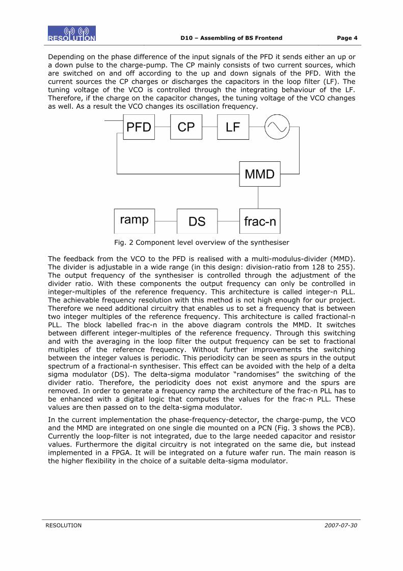
2 Overview of RF frontend architecture
Fig. 1 gives a system overview of the RF Frontend with its three different major building blocks. The port on the left side connects to the antenna, while the right side ports represent the signal and control connections to the baseband.
Fig. 1 RF frontend overview
The RF frontend consists of three major subsystems. The frequency synthesizer equally connects to the receiver side LNA and mixer combination as well as to the transmitter side power amplifier module. It creates a frequency ramp that either is transmitted through the power amplifier to the antenna or serves as a local oscillator for the receiver subsystem.
The overall RF frontend then connects to the antenna and the baseband circuitry. The measurement equipment has been connected to these interfaces and the key performance characteristics have been extracted.
3 Synthesiser architecture The synthesiser is based on a fractional-n PLL (Fig. 2) [6]. It consists of a phase-frequency detector (PFD), which compares the phases of the reference input signal and the output of the divided voltage controlled oscillator (VCO) signal. The outputs of the PFD are two pulse width modulated signals, which control the charge-pump (CP).
D10 – Assembling of BS Frontend Page 4
RESOLUTION 2007-07-30
Depending on the phase difference of the input signals of the PFD it sends either an up or a down pulse to the charge-pump. The CP mainly consists of two current sources, which are switched on and off according to the up and down signals of the PFD. With the current sources the CP charges or discharges the capacitors in the loop filter (LF). The tuning voltage of the VCO is controlled through the integrating behaviour of the LF. Therefore, if the charge on the capacitor changes, the tuning voltage of the VCO changes as well. As a result the VCO changes its oscillation frequency.
Fig. 2 Component level overview of the synthesiser
The feedback from the VCO to the PFD is realised with a multi-modulus-divider (MMD). The divider is adjustable in a wide range (in this design: division-ratio from 128 to 255). The output frequency of the synthesiser is controlled through the adjustment of the divider ratio. With these components the output frequency can only be controlled in integer-multiples of the reference frequency. This architecture is called integer-n PLL. The achievable frequency resolution with this method is not high enough for our project. Therefore we need additional circuitry that enables us to set a frequency that is between two integer multiples of the reference frequency. This architecture is called fractional-n PLL. The block labelled frac-n in the above diagram controls the MMD. It switches between different integer-multiples of the reference frequency. Through this switching and with the averaging in the loop filter the output frequency can be set to fractional multiples of the reference frequency. Without further improvements the switching between the integer values is periodic. This periodicity can be seen as spurs in the output spectrum of a fractional-n synthesiser. This effect can be avoided with the help of a delta sigma modulator (DS). The delta-sigma modulator “randomises” the switching of the divider ratio. Therefore, the periodicity does not exist anymore and the spurs are removed. In order to generate a frequency ramp the architecture of the frac-n PLL has to be enhanced with a digital logic that computes the values for the frac-n PLL. These values are then passed on to the delta-sigma modulator.
In the current implementation the phase-frequency-detector, the charge-pump, the VCO and the MMD are integrated on one single die mounted on a PCN (Fig. 3 shows the PCB). Currently the loop-filter is not integrated, due to the large needed capacitor and resistor values. Furthermore the digital circuitry is not integrated on the same die, but instead implemented in a FPGA. It will be integrated on a future wafer run. The main reason is the higher flexibility in the choice of a suitable delta-sigma modulator.
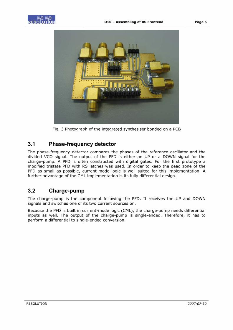
D10 – Assembling of BS Frontend Page 5
RESOLUTION 2007-07-30
Fig. 3 Photograph of the integrated synthesiser bonded on a PCB
3.1 Phase-frequency detector The phase-frequency detector compares the phases of the reference oscillator and the divided VCO signal. The output of the PFD is either an UP or a DOWN signal for the charge-pump. A PFD is often constructed with digital gates. For the first prototype a modified tristate PFD with RS latches was used. In order to keep the dead zone of the PFD as small as possible, current-mode logic is well suited for this implementation. A further advantage of the CML implementation is its fully differential design.
3.2 Charge-pump The charge-pump is the component following the PFD. It receives the UP and DOWN signals and switches one of its two current sources on.
Because the PFD is built in current-mode logic (CML), the charge-pump needs differential inputs as well. The output of the charge-pump is single-ended. Therefore, it has to perform a differential to single-ended conversion.

D10 – Assembling of BS Frontend Page 6
RESOLUTION 2007-07-30
Fig. 4 Simplified charge-pump
3.3 Loop filter The loop-filter of the PLL is not yet completely integrated. Only a small capacitor connected to the tuning voltage of the VCO is currently integrated. The main reason for not integrating the loop-filter is to achieve high flexibility. The behaviour of the PLL significantly depends on the loop-filter. Therefore, it is advantageous for testing purposes to be able to modify it easily.
A small PCB for the loop filter was developed. It can directly be connected either to a wafer probe or to the PLL PCB. Several of these PCBs were fabricated and assembled with different resistor and capacitor values.
Fig. 5 PCB with loop filter
3.4 MMD architecture The Multi-modulus divider (MMD) consists of several DIV-2/3 blocks. Each of these blocks can either divide the input signal by two or by three. The used divider has seven cascaded DIV-2/3 stages so that a division ration between 128 and 255 can be set. All inputs controlling the division ratio of the MMD are connected to pads and can be

D10 – Assembling of BS Frontend Page 7
RESOLUTION 2007-07-30
controlled by external circuitry, e.g. an FPGA. With this implementation the PLL can work in integer-n as well as fractional-n mode.
Fig. 6 Divide stage (2/3) of multi-modulus divider
given by the quality factor of the LC-tank. Thus for the same LC-tank the tail current of the gm-boosted VCO can be reduced compared to the classical Colpitts-oscillator.
3.5 VCO architecture Due to the stringent requirements for phase-noise of the VCO in communication and positioning systems, mainly LC oscillator topologies were investigated. To overcome the drawbacks of both the crosscoupled and the Colpitts oscillator a new topology published by Xiaoyong Li et al [1] [2]has been used. This topology is based on a Colpitts-VCO in common-gate configuration. The gates of the transistors are not connected to a constant biasing voltage like in the case of a conventional Colpitts-oscillator. Instead at the gate a voltage that has a phase shift of 180° to the voltage at the LC-tank is applied. If the transistor is switched off, the non-constant biasing voltage has no effect on the circuit operation. But when the transistor is switched on to compensate the losses in the LC-tank the gate-source voltage is twice as high as it would be with constant biasing. Therefore the effective transconductance is increased. The required effective transconductance is

D10 – Assembling of BS Frontend Page 8
RESOLUTION 2007-07-30
Fig. 7 Architecture of the VCO
In analogue radio frequency integrated circuits the VCO is usually built with a differential architecture to reduce the effect of substrate noise coupling. This is a great advantage for the gm-boosted VCO. A voltage with the necessary phase-shift and amplitude that is sufficiently large is available at the other path of the VCO. The gate can either be
e other transistor. It is advantageous to iasing is necessary then.
> 10 dB) peration time ( > 20%)
duce interferences with other channels ( OIP3 > 300 mW) atching (S11,S22 < - 7 dB)
e unconditionally stable (KF > 1)
During the last year, several different Power amplifier architectures have been realized that offer different advantages and drawbacks concerning output power, gain and efficiency [5]. The implementations have been implemented in order to be able to
connected to the source or the drain of thconnect it the drain as no further b
4 Transmitter Architecture The specifications for the base band transmitter module are as following:
1. High output power to achieve sufficient coverage range ( > 12 dBm) 2. High amplification of at least 10 dB (Gain S21
3. High power added efficiency PAE to maximise o4. High linearity to re5. Input and Output m6. The circuit has to b
In order to reach these values, different power amplifier (PA) architectures have been developed and implemented, the most promising one tested and measured on a specific printed wire board. This subsystem has then later on been integrated into the demonstrator realization. The transmitter module consists of a Power amplifier (PA), a DC switch and switches that connect this subsystem to the overall system. The most prominent part of the transmitter, the PA will be discussed in the following subchapter.
4.1 PA architectures

D10 – Assembling of BS Frontend Page 9
RESOLUTION 2007-07-30
of merit against each other and to e base station transmitter
Tw osen for further investigation and will be ady obtained results. These two are the Class output power figures, for moderate to good ter one shows a smaller small signal gain
fi The Class E PA realization showed unstable e moment. The simulation results for the
her advancement versus the Class A or F PA more risky in the implementation, was also
no o test transmitter, one uses the Class A PA, emented and then extensively measured.
Fig. 8 shows visible in the layout, the ground plane has been realized as vast as possible in order to keep the inductive degeneration effect small. Fig. 9 shows the simulated versus measured key parameters of the bare die. The measurement results were obtained using on wafer measurements; the simulated results include the extracted parasitic resistive and capacitive elements of the layo ld be quite close to reality.
compare under real world conditions these figure choose the most suitable PA architecture for use in th
Realized have been these following architectures:
• Class A PA • Class E PA • Class F PA • Dynamic Input Biasing PA
o of these architectures were then chredesigned in the future to optimize the alreA power amplifier that offers good gain and efficiency values and the Class F PA. The lagure but offers a very high efficiency.
behaviour and was therefore omitted at thDynamic input biasing PA showed no furtdesign and, being more complex and thereby
further investigated. In the following, twthe second using the Class F PA, were impl
4.2 Characterisation of Class A PA the circuit schematic and layout of the Class A power amplifier. As
ut and shou
Fig. 8 Circuit schematic and Layout for Class A power amplifier
D10 – Assembling of BS Frontend Page 10
RESOLUTION 2007-07-30
Ghz Ghz
Ghz dBm
S11 S22
Measured
Simulated
Measured
Simulated
Simulated
Measured
Simulated
Measured
PS 1dB 21
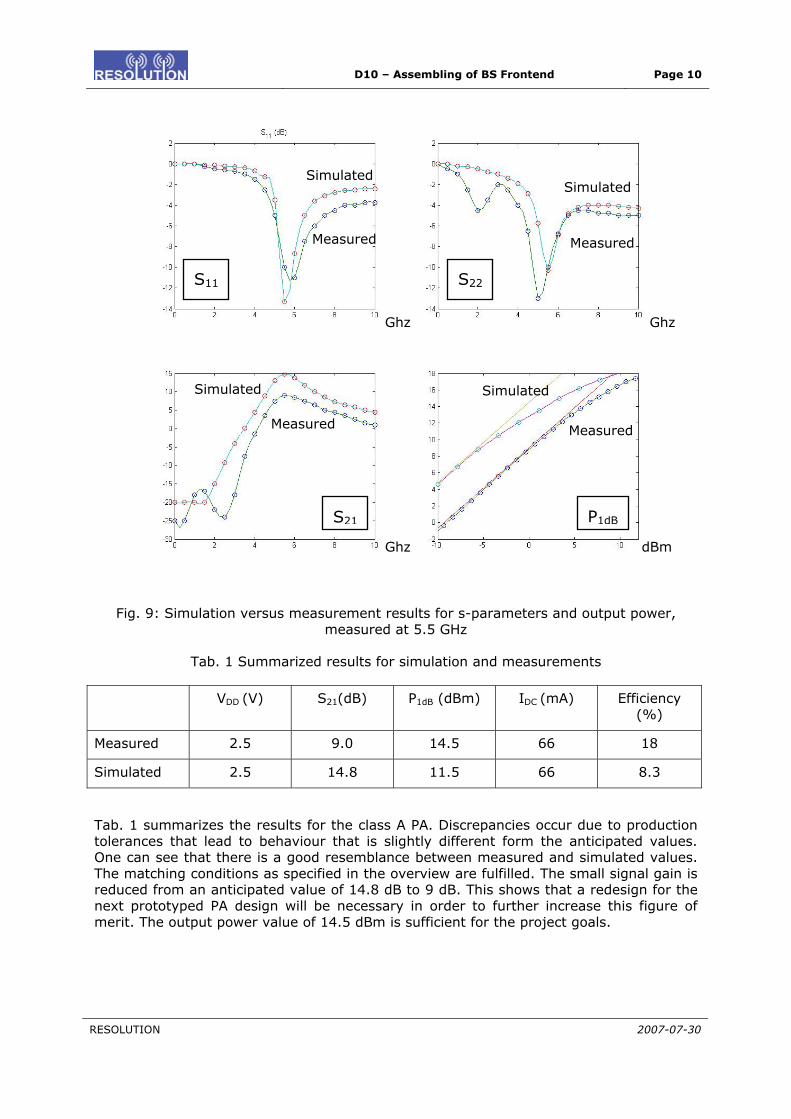
Fig. 9: Simulation versus measurement results for s-parameters and output power, measured at 5.5 GHz
Tab. 1 Summarized results for simulation and measurements
VDD (V) S2 P1dB (dBm) IDC (mA) Efficiency )
1(dB)(%
Measured 2.5 9.0 14.5 66 18
Simulated 2.5 14.8 11.5 66 8.3
Tab. 1 summarizes the results for the class A PA. Discrepancies occur due to production tolerances that lead to behaviour that is slightly different form the anticipated values. One can see that there is a good resemblance between measured and simulated values. The matching conditions as specified in the overview are fulfilled. The small signal gain is reduced from an anticipated value of 14.8 dB to 9 dB. This shows that a redesign for the next prototyped PA design will be necessary in order to further increase this figure of merit. The output power value of 14.5 dBm is sufficient for the project goals.

D10 – Assembling of BS Frontend Page 11
RESOLUTION 2007-07-30
4.3 Characterisation of Class F PA Fig. 10 shows the layout and schematic representation, Fig. 11 shows the measured versus simulated results for the Class F power amplifier.
Fig. 10 Layout and schematic representation of the Class F power amplifier
0 2 4 6 8 10−40
−35
−30
−25
−20
−15
−10
−5
0
Frequency
0 2 4 6 8 10−40
−35
−30
−25
−20
−15
−10
S11
measured
S11
simulated
−5
0
Frequency
S22
measured
S22
simulated
Input matching S11 Output matching S22
0 2 4 6 8 10−20
−15
−10
−5
0
5
10
Frequency
S21
measured
S21
simulated
−20 −15 −10 −5 0 5 10 15
−10
0
10
20
30
40
Class F 1dB Compression Point = 17.25 dBm @ 43.05% Efficiency
P1dB
measured = 17.25 dBm
Efficiency measured = 43.05 %P
1dB simulated = 18.24 dBm
Pin
(dBm)
Gain S21 1 dB compression point, efficiency
Fig. 11 S-parameter simulations and measurements, output power measured at 5.8 GHz
The measurements results for the class F power amplifier show that especially two parameters qualified this chip for a further investigation as a part of the transmitter subsystem. For once, it delivers a very satisfying 17.25 dBm output power, associated

D10 – Assembling of BS Frontend Page 12
RESOLUTION 2007-07-30
with a gain of above 8.4 dB. Most importantly, the measured drain efficiency was measured to be 43.1 % at the 1 dB compression point, which is thus far the highest efficiency value achieved.
One can see that the high consistency between measured and simulated results for the S11–parameters, while for the S11–parameters, the measured matching peak is shifted slightly towards lower frequencies. The wave shaping due to the output filter was already explained in former reports and is well known in literature. Fig. 11 shows the measured and simulated S parameter and output power plots. For this amplifier, the measured and simulated S11 parameters precisely agree. The measured S22 parameters also closely match the predicted values; however, the measured matching peak is slightly shifted towards lower frequencies. The small signal gain plots show a similar good general resemblance between measured and simulated results, the measured gain around 5.5 GHz achieves, however only 8.4 dB, which is almost 3 dB below the predicted value. A redesign of this circuit will follow for the next run. The 1 dB compression point is reduced by about 1 dBm between measured and simulated values, which is a satisfyingly small difference.
4.4 Realization printed wire boards
itching of the RF signals at the input and output.
Fig. 12 shows the printed wire board for the Class A transmitter. Several design aspects had to be taken into account. For the time being, the RF switch that will later be part of the integrated circuit and separates RF input and output port that send and receive over the same antenna, is not integrated. This is due to the fact that for once, this is not a critical element of the transmitter system and can be easily realized using discrete elements for measurement purposes. Besides, the transmitter subsystem can be driven over one separate port. Only when the overall RF front-end system will be assembled, one has to take care of the sw
Fig. 12 Printed wire board for Class A based transmitter
The printed wire boards contains four SMA connectors that are used to connect the PA die with the DC supply voltage (upper and lower SMA connectors), the bias voltage as well as RF input and output (left and right SMA connectors). One can distinguish the PA die centred in the printed wire board. The DC switch enables the on and off switching of the power amplifier in order to realize energy savings if the transmitter stage is not needed. The corresponding DC switch IC is placed between the upper SMA connector and

D10 – Assembling of BS Frontend Page 13
RESOLUTION 2007-07-30
the PA die. Three pin connectors are needed in order to control the DC switch. The size of the PWB is 28 mm x 28 mm.
Fig. 13 Printed wire board for Class F based transmitter
Fig. 13 shows the printed wire board for the Class F power amplifier. Input and Output SMA Connectors are on the left and right side, the DC and bias voltage supply is on the upper side of the PWB. The design of the PWB is similar to the former one, included is the DC as well as RF shunt capacitances in the DC paths in order to suppress possible spurious RF signals through the supply lines. The size of the printed wire board is 28 mm x 22 mm.
The key parameters of the chosen DC switch have to fulfil several important aspects. For once, the seen resistance of the turned on DC switch has to be as small as possible in order to avoid additional losses in the DC switch. On the other hand, the off resistance of the DC switch has to be extremely high to really turn the PA of. The range of the possible DC supply voltages that the IC can support should be as large as possible, in any case between 1.9 to 2.4 V, as the actual PA’s applies these voltage values.
The chosen DC switch IC is one from Analogue Devices, called ADG801. It offers a very low on resistance of 0.26 Ω and supports supply voltages between 1.8 and 5.5 V. The switching time is 35 ns and therefore a very small value which should accommodate actual needs.
4.5 Class A based transmitter subsystem with DC switch
Fig. 14 show he mounted DC switch IC, Fig. 15 the corresponding measured key figures of merit. One can see that the matching conditions are barely affected, which also was not expected due to the DC blocking capacitances in the DC supply path. The small signal gain is slightly decreased to around 7.2 dB which occurs due to the fact that a small part of the DC supply voltage is lost through the on resistance of the DC switch. The measured 1 dB compression point is significantly decreased from the former measured 19.8 dBm (deliverable D5) down to 13 dBm, the explanation for this at the time being seems to be an influence of the DC switch to the PA circuitry. Although the measured value stays above the aimed specification, the next subsystem assembly will integrate the DC switch and thereby the discrepancy should be nullified.
s the picture of the Class A based transmitter subsystem with t

D10 – Assembling of BS Frontend Page 14
RESOLUTION 2007-07-30
Fig. 14 Test-board for Class A based transmitter with DC switch
1 2 3 4 5 6 7 81 2 3 4 5 6 7 8
0 0
x 109
−20
−15
−10
−5
Frequency (GHz)
Inpu
t Ref
lect
ion
Coe
ffici
ents
(dB
)
S11
measured
x 109
−20
−15
−10
−5
Out
put R
efle
ctio
n C
oeffi
cien
ts (
dB)
S measured22
22
Frequency (GHz)
Input matching S11 Output matching S
1 2 3 4 5 6 7 8
x 109
−20
−15
−10
−5
0
5
10
Frequency (GHz)
Sm
all s
igna
l gai
n (d
B)
S21
measured
−20 −15 −10 −5 0 5 10
−15
−10
−5
0
5
10
15
20
Pin
(dBm)
Pou
t (dB
m),
Effi
cien
cy (
%)
P1dB
measured = 13.0 dBm
Gain S21 1 dB compression point, efficiency
Fig. 15 S-parameter board measurements, output power measured at 5.8 GHz
D10 – Assembling of BS Frontend Page 15
RESOLUTION 2007-07-30
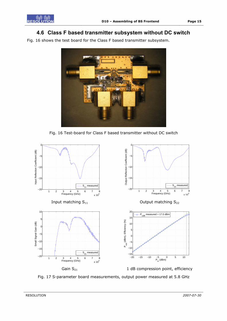
4.6 Class F based transmitter subsystem without DC switch Fig. 16 shows the test board for the Class F based transmitter subsystem.
Fig. 16 Test-board for Class F based transmitter without DC switch
0
1 2 3 4 5 6 7 8
x 109
−20
−15
0
−10
−5
Frequency (GHz)
Inpu
t Ref
lect
ion
Coe
ffici
ent (
dB)
S11
measured
1 2 3 4 5 6 7 8
x 109
−20
−15
−10
Frequency (GHz)
Out
put R
efle
ctio
n C
oeffi
cien
t (dB
)
−5
S22
measured
Input matching S11 Output matching S22
−20 −15 −10 −5 0 5 10−15
−10
−5
0
5
10
15
20
1 2 3 4 5 6 7 8
x 109
−20
−15
−10
−5
0
5
10
Frequency (GHz)
Sm
all S
igna
l Gai
n (d
B)
S21
measured
Pin
(dBm)
Pou
t
(dB
m),
Effi
cien
cy (
%)
P1dB
measured = 17.0 dBm
Gain S21 1 dB compression point, efficiency
Fig. 17 S-parameter board measurements, output power measured at 5.8 GHz

D10 – Assembling of BS Frontend Page 16
RESOLUTION 2007-07-30
necessary any more.
The obtained measurement results are displayed in Fig. 17. One can see that the input ery good for the frequency range between 5 and 6 GHz. ignal gain is shifted towards lower frequency and strongly
ecreases towards 6 GHz. Furthermore, the maximum value for the small signal gain aches only 6.5 dB at 5 GHz. Analogously, a redesign will have to increase this figure of
merit. The obtained 1 dB compression point alue of 17 dBm is only 0.25 dBm below the measured value for the on wafer measured Class F PA and thereby largely surpasses the necessary 12 dBm for the transmitter subsystem.
5 Receiver Architecture
5.1 Introduction
In this part of the report, the characteristics of two versions of the implemented receiver are presented. In order to characterize the specific receiver features like power gain, noise figure and linearity, VCO-Receiver subsystem was implemented using the same receiver version as presented in deliverable D6 [3][4]. At the same time, a receiver prototype with off-chip components like balun, filter and VGA is developed and characterized to verify the complete receiver concept. After introducing the new standalone receiver perfo of subsystems will be explained in detail. The complet techniques will be
For the Class F based transmitter subsystem, the DC switch has not integrated at the time being as the circuit itself delivers already insufficient small signal gain and no additional extracted knowledge would have resulted. The DC switch will be integrated in the next design run into the integrated PA circuitry so that an additional discrete DC switching will not be
and output port matching is vHowever, the measured small sdre
v
rmances, the experimental analysise measurement setup and applied
presented as well.
5.2 Receiver core
Fig. 18 RF board of the receiver core
D10 – Assembling of BS Frontend Page 17
RESOLUTION 2007-07-30
Fig. 18 shows the suitable for the characterisation of the subsystem power gain, noise figure and linearity since it is a complete Th stand alone receiver have been already presented D6 r analyses have been performed and new results are presented. rises a f integrated LNA and mixer. The details of t rcuits can be found in D6.
By using the LECROY WaveSurfer 424 and the A 6C ENR head phase imbalance of the output signal was analysed and the Noise Figure down to 100 kHz was measured. In the oscilloscope analysis, a systematic erro entified due to the different lengths of th rip lines on the PCB board which the LO signal for the mixer. This length ce caused a phase imbalance e direct influence was an overall l version gain and higher noise of er. This phase imbalance has been nally compensated with two p fters. The minor layout level imbalances are also adjusted through these e ase shifters. This resulted in comparativ ter performances as will be shown erable.
Measurement setup comprises Agilent HP 83650A signal generators for RF and LO ignals. 180° hybrid couplers are used for unbalanced to balanced signal conversion and
Parameter Measured values
PCB of the implemented receiver core which is very
50 Ω system.in deliverable
e features of the . Meanwhile, furthe
The receiver core comphe PCB and ci
ully
gilent 34
r has been idfeed e microst
differenower con
in the circuit, whos the receiv
exter hase shixternal ph
ely bet in this deliv
svice versa. Fig. 19 presents the receiver core performances at 1.8 V for the mixer and 3.3 V for the LNA and RF at 5.8 GHz and LO at 5.805 GHz swept from the correspondingly the IF at 5 MHz. The overall power consumption is 75 mW.
Tab. 2 Receiver core performances at optimum bias
Noise figure 8,5 dB
RF Gain 15,5 dB
IP1dB - 18,75 dBm
IIP3 -13,5 dBm
S11 < -7 dB
S22 < -20 dB
As shown in Tab. 2, the increase in the gain and decrease in the noise figure values compared to the previous results are due to the above mentioned reasons. Though the performances are comparatively better further improvements in the noise figure and gain values are expected in the following implementations. Fig. 19 shows output power variations as a fu -18.75 dBm. eing fixed at
nction of input power of their receiver showing 1 dB gain compression atThe output power is measured at 5 MHz IF and LO power b
0 dBm approximately. Same LO power level has been used for all of our measurements.
D10 – Assembling of BS Frontend Page 18
RESOLUTION 2007-07-30
-45 -40 -35 -30 -25 -20 -15-30
-25
-20
-15
-10
-5
0
Out
put P
ower
[dBm
]
Input Power [dBm]
C ESG as signal generator along with Agilent E4440A PSA
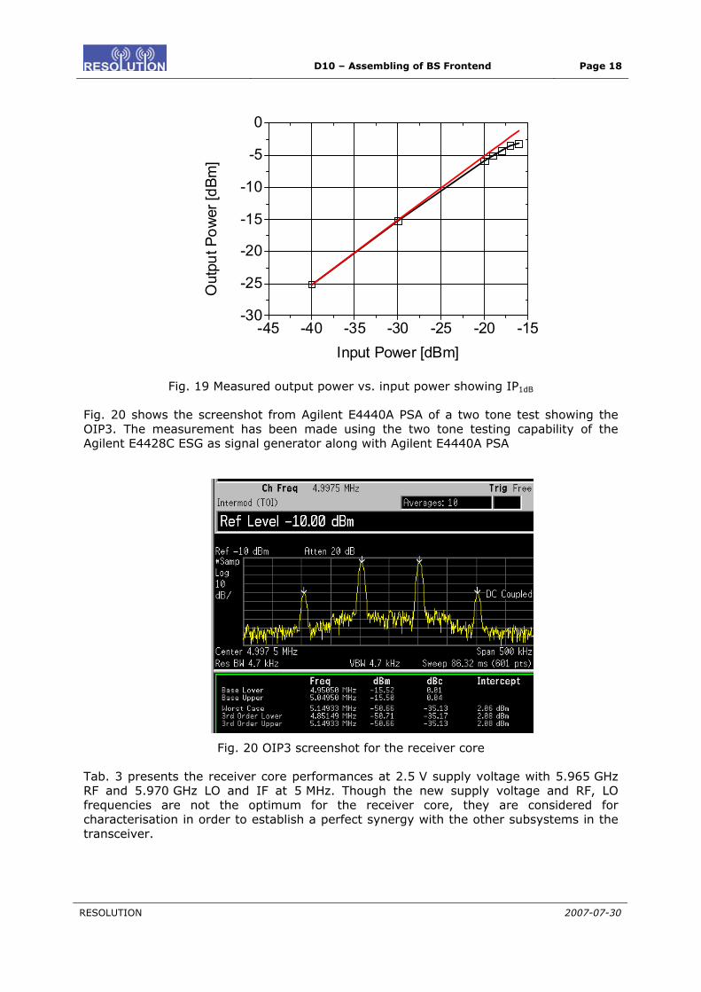
Fig. 19 Measured output power vs. input power showing IP1dB
Fig. 20 shows the screenshot from Agilent E4440A PSA of a two tone test showing the OIP3. The measurement has been made using the two tone testing capability of the Agilent E4428
Fig. 20 OIP3 screenshot for the receiver core
Tab. 3 presents the receiver core performances at 2.5 V supply voltage with 5.965 GHz RF and 5.970 GHz LO and IF at 5 MHz. Though the new supply voltage and RF, LO frequencies are not the optimum for the receiver core, they are considered for characterisation in order to establish a perfect synergy with the other subsystems in the transceiver.

D10 – Assembling of BS Frontend Page 19
RESOLUTION 2007-07-30
Tab. 3 Receiver core performances at 2.5 V supply
Parameter Measured Values
Noise figure ~ 9 dB
RF Gain 11,5 dB
IP1dB -17,75 dBm
IIP3 -8,7 dBm
The OIP3 results under similar measurement conditions are presented in Fig. 21.
Fig. 21 OIP3 screenshot for the receiver core at 2.5 V
6 Integration of VCO with Receiver
In this part the performances of the whole receiver frontend are summarised. The results compromise a detailed characterisation of the receiver core with the VCO subsystem. Furthermore, the characteristics of the receiver PCB with off-chip components like input filter, balun, LO buffers and VGA together with VCO subsystem will be presented. With this off-chip component version, the complete receiver functionality can be verified which includes the dynamic range adjustments by varying the control voltage of the VGA. The gain control of the VGA and hence the dynamic range of the receiver is facilitated by an additional control voltage pin which is supplied externally to a power supply.

D10 – Assembling of BS Frontend Page 20
RESOLUTION 2007-07-30
VCOsubsystem eceiver
coreR
LO buffer Rat-ra
couplerce
VCOsubsystem eceiver
coreR
LO buffer Rat-ra
coupler
s in using the fully differential output of the VCO. The complete system including VCO is characterized with 2.5 V supply voltage. The VCO reference frequency is set for LO frequency of 5.970 GHz, RF is at 5.965 GHz and IF at 5 MHz.
Tab. 4 Receiver core performances with VCO
Parameter Measured Values
ce
Fig. 22 Receiver core with VCO subsystem
Fig. 22 shows the setup with the PCB of the receiver core and VCO subsystem of the synthesiser. From left to the right in the figure, the VCO subsystem with externally cascaded amplifiers (Minicircuits Type ZX60-8008E-S+) for delivering the required LO signal level to the mixer LO input, phase shifters and a PCB implemented rat race coupler for single to differential conversion followed by phase shifters is assembled. The rat-race couplers have been used due to some technical difficultie
Noise figure ~ 9.4 dB
RF Gain 10,5 dB
IP1dB ~ - 15,5 dBm
IIP3 ~-10 dBm
Tab. 4 summarises the experimental results of the subsystem shown in Fig. 22. Using the VCO subsystem instead of an ideal LO source, a slight decrease in conversion gain can be observed and a slightly higher noise figure. The differences are due to an impedance mismatch between the VCO output and mixer LO input. However, the overall system performances are satisfactory and the functionality of the subsystems connected to a receiver path has been verified. However, optimisation is still possible that was coordinated on the RFIC meeting for the next wafer runs.

D10 – Assembling of BS Frontend Page 21
RESOLUTION 2007-07-30
Fig. 23 Receiver core with off-chip VGA and VCO subsystem
measurement results under two conditions of the control voltage where VGA GA and hence the complete in VGA datasheet, since the
iver, transmitter and synthesiser subsystem).
nge of the complete receiver chain at 2.5 V. The
Fig. 23 shows the setup with the PCB of the receiver with off-chip components and VCO subsystem. The measurement setup and settings are similar to the previous one. Tab. 5 presents the has ~0 dB and maximum gain. As can be concluded, the Vchain does not have the full scale gain variations as specifiedwhole PCB is operating at 2.5 V (for maintaining the synergy between the rece
Tab. 5 shows the achieved dynamic raperformances decreased due to the non-optimum supply voltage and shifted RF and LO frequencies.
Tab. 5 Performances of complete receiver chain with VCO
Parameter Measured values
Voltage Gain
@Vctrl=0.1 V 9 dB
Voltage Gain
@Vctrl = 0.5 V
24,5 dB
Voltage gain
@Vctrl = 1 V 42,6 dB
IP1dB - 16 dBm
D10 – Assembling of BS Frontend Page 22
RESOLUTION 2007-07-30
The above results show the integration capability of the subsystems. With some minor variations in the design aspect it shows the possibility for an optimum system performance at a unified measurement conditions. This aspect is strongly under investigation for the next waferruns considering the characteristics and influence of the synthesiser.
7 Integration of VCO with Transmitter
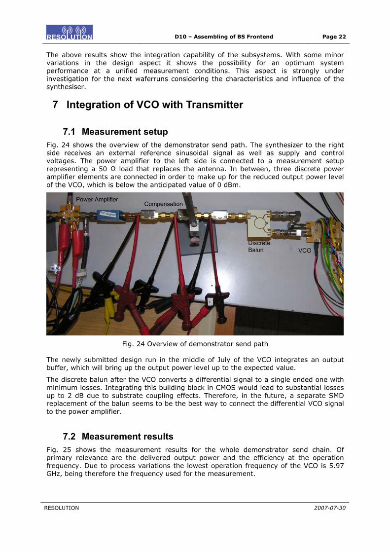
7.1 Measurement setup Fig. 24 shows the overview of the demonstrator send path. The synthesizer to the right side receives an external reference sinusoidal signal as well as supply and control voltages. The power amplifier to the left side is connected to a measurement setup representing a 50 Ω load that replaces the antenna. In between, three discrete power amplifier elements are connected in order to make up for the reduced output power level of the VCO, which is below the anticipated value of 0 dBm.
Fig. 24 Overview of demonstrator send path
The newly submitted design run in the middle of July of the VCO integrates an output buffer, which will bring up the output power level up to the expected value.
The discrete balun after the VCO converts a differential signal to a single ended one with minimum losses. Integrating this building block in CMOS would lead to substantial losses up to 2 dB due to substrate coupling effects. Therefore, in the future, a separate SMD replacement of the balun seems to be the best way to connect the differential VCO signal to the power amplifier.
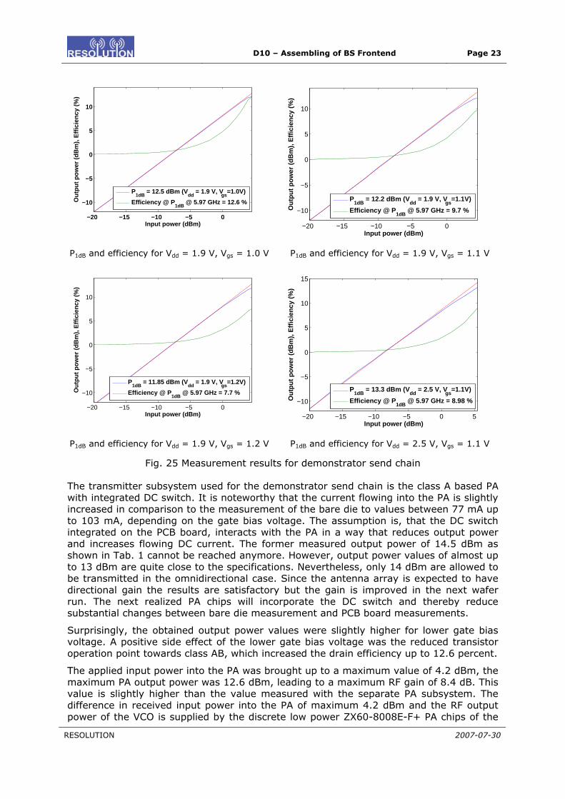
7.2 Measurement results Fig. 25 shows the measurement results for the whole demonstrator send chain. Ofprimary relevance are the delivered output power and the efficiency at the operation
w GHz, being therefore the frequency used for the measurement.
frequency. Due to process variations the lo est operation frequency of the VCO is 5.97
D10 – Assembling of BS Frontend Page 23
RESOLUTION 2007-07-30
−20 −15 −10 −5 0
−10
−5
0
5
10
Input power (dBm)
Ou
tpu
t p
ow
er (
dB
m),
Eff
icie
ncy
(%
)
P1dB
= 12.5 dBm (Vdd
= 1.9 V, Vgs
=1.0V)
Efficiency @ P1dB
@ 5.97 GHz = 12.6 %
−20 −15 −10 −5 0
−10
−5
0
5
10
Input power (dBm)
Ou
tpu
t p
ow
er (
dB
m),
Eff
icie
ncy
(%
)
P1dB
= 12.2 dBm (Vdd
= 1.9 V, Vgs
=1.1V)
Efficiency @ P1dB
@ 5.97 GHz = 9.7 %
P1dB and efficiency for Vdd = 1.9 V, Vgs = 1.0 V P1dB and efficiency for Vdd = 1.9 V, Vgs = 1.1 V
−20 −15 −10 −5 0
−10
−5
0
5
10
Input power (dBm)
Ou
tpu
t p
ow
er (
dB
m),
Eff
icie
ncy
(%
)
−20 −15 −10 −5 0 5
−10
−5
0
5
10
15
Input power (dBm)
Ou
tpu
t p
ow
er (
dB
m),
Eff
icie
ncy
(%
)
P1dB
= 13.3 dBm (Vdd
= 2.5 V, Vgs
=1.1V)
Efficiency @ P1dB
@ 5.97 GHz = 8.98 %
P1dB
= 11.85 dBm (Vdd
= 1.9 V, Vgs
=1.2V)
Efficiency @ P1dB
@ 5.97 GHz = 7.7 %
P1dB and efficiency for Vdd = 1.9 V, Vgs = 1.2 V P1dB and efficiency for Vdd = 2.5 V, Vgs = 1.1 V
Fig. 25 Measurement results for demonstrator send chain
The transmitter subsystem used for the demonstrator send chain is the class A based PA with integrated DC switch. It is noteworthy that the current flowing into the PA is slightly increased in comparison to the measurement of the bare die to values between 77 mA up to 103 mA, depending on the gate bias voltage. The assumption is, that the DC switch integrated on the PCB board, interacts with the PA in a way that reduces output power and increases flowing DC current. The former measured output power of 14.5 dBm as shown in Tab. 1 cannot be reached anymore. However, output power values of almost up to 13 dBm are quite close to the specifications. Nevertheless, only 14 dBm are allowed to
ext wafer n. The next realized PA chips will incorporate the DC switch and thereby reduce
ubstantial changes between bare die measurement and PCB board measurements.
Surprisingly, the obtained output power values were slightly higher for lower gate bias voltage. A positive side effect of the lower gate bias voltage was the reduced transistor operation point towards class AB, which increased the drain efficiency up to 12.6 percent.
The applied input power into the PA was brought up to a maximum value of 4.2 dBm, the maximum PA output power was 12.6 dBm, leading to a maximum RF gain of 8.4 dB. This value is slightly higher than the value measured with the separate PA subsystem. The difference in received input power into the PA of maximum 4.2 dBm and the RF output power of the VCO is supplied by the discrete low power ZX60-8008E-F+ PA chips of the
be transmitted in the omnidirectional case. Since the antenna array is expected to have directional gain the results are satisfactory but the gain is improved in the nrus

D10 – Assembling of BS Frontend Page 24
RESOLUTION 2007-07-30
producer mini-circuits. The goal for the next chip samples is to increase the RF gain by around 4 dB in order to achieve the 12 dBm output power with an input power value of 0 dBm of the VCO, which will be its target value.
The output power peak plot of the PA is similar to the one shown in Fig. 26. The whole frequency spectrum was considered and no additional peaks were detected.
Fig. 26 Output power plot similar to the ones measured in demonstrator send chain
8 Conclusions First prototypes for the synthesiser, the transmitter and the receiver in advanced CMOS technology have been realised. Printed circuit boards (PCBs) for the separate components have been developed and the prototype-ICs are bonded on these PCBs. For this deliverable report, the transmitter PCB and the receiver PCB are connected to the synthesiser subsystem in order to operate as a complete base station frontend for the RESOLUTION demonstrator.
complete receiver and transmitter frontend was verified in this
ptimised in the following wafer runs until the end of the project. Consequently, the three subsystems can now be highly integrated to achieve
December 2005.
The functionality of the deliverable. Especially, the characteristics of the whole RF frontend have been determined by means of measurements and bottlenecks were identified. Based on these results, the whole frontend can be o
a compact demonstrator at the end of the project.
9 References [1] X. Li, S. Shekr, and D. J. Allstot, “Low-power gm-boosted LNA and VCO,” in Digest
of Technical Papers 2005 IEEE International Solid-State Circuit Conference, vol. 1, pp. 534–615, February 2005.
[2] X. Li, S. Shekr, and D. J. Allstot, “gm-boosted common-gate LNA and differential Colpitts VCO/ QVCO in 0,18μm CMOS,” IEEE Journal of Solid-State Circuits, vol. 40, pp. 2609–2618,
[3] V. Subramanian, S. Spiegel, R. Eickhoff and G. Boeck, “A CMOS Low Noise Amplifier for 5 to 6 GHz Wireless Applications”, sub. to IEEE International Microwave and Optoelectronic Conference, Oct./Nov. 2007.
D10 – Assembling of BS Frontend Page 25
RESOLUTION 2007-07-30
[5] J .Carls, F. Ellinger, R. Eickhoff, P. Sakalas, S von der Mark and S. Wehrli, “Design of a C-Band CMOS Class AB Power Amplifier for an Ultra Low Supply Voltage”, in Proceedings of the International Microwave and Optoelectronics Conference (IMOC), 2007.
[6] T. Ußmüller, K. Seemann and R. Weigel, “gm-boosted VCO with low power consumption and large tuning range”, in Proceedings of 10th European Conference on Wireless Technology, 2007.
[4] M. Krcmar, S. Spiegel, F. Ellinger and G. Boeck, “A Broadband Folded Gilbert-Cell CMOS Mixer”, sub. to IEEE International Conference on Electronics, Circuits and Systems, 2007.