cse140: components and design techniques for digital...
TRANSCRIPT

Sources: TSR, Katz, Boriello & Vahid
1
CSE140: Components and Design Techniques
for Digital Systems
Latches and flip-flops
Tajana Simunic Rosing
Sources: Katz, Boriello & Vahid
Sources: TSR, Katz, Boriello & Vahid
2
Where we are now
• What we’ve covered so far – Combinational circuits: Chap 1,2
• HW#5 out
• What comes next: – Chap 3: Sequential circuits
Sources: TSR, Katz, Boriello & Vahid
3
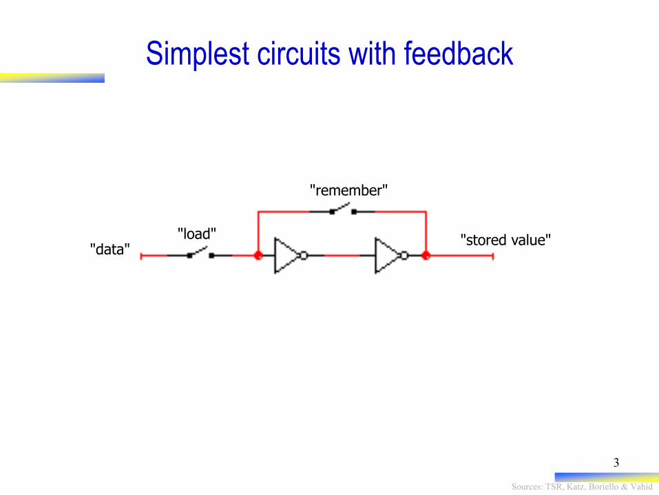
"remember"
"load" "data"
"stored value"
Simplest circuits with feedback
Sources: TSR, Katz, Boriello & Vahid
4
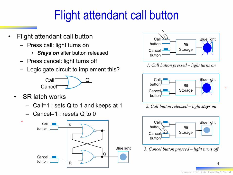
Flight attendant call button
• Flight attendant call button
– Press call: light turns on
• Stays on after button released
– Press cancel: light turns off
– Logic gate circuit to implement this?
Q Call
Cancel a
a
Bit
Storage
Blue light Call
button
Cancel
button
1. Call button pressed – light turns on
Bit
Storage
Blue light Call
button
Cancel
button
2. Call button released – light stays on
Bit
Storage
Blue light Call
button
Cancel
button
3. Cancel button pressed – light turns off
• SR latch works
– Call=1 : sets Q to 1 and keeps at 1
– Cancel=1 : resets Q to 0
R
S
Q
C all
but t on
Blue lig h t
C an c el but t on
Sources: TSR, Katz, Boriello & Vahid
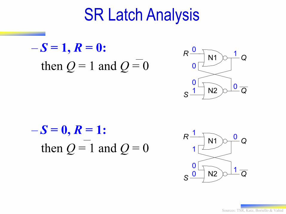
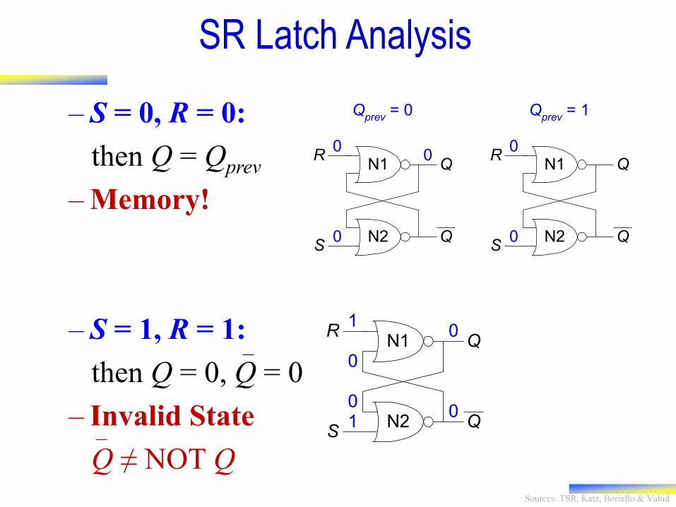
– S = 1, R = 0:
then Q = 1 and Q = 0
– S = 0, R = 1:
then Q = 1 and Q = 0
SR Latch Analysis
R
S
Q
Q
N1
N2
0
1
1
00
0
R
S
Q
Q
N1
N2
1
0
0
10
1
Sources: TSR, Katz, Boriello & Vahid
R
S
Q
Q
N1
N2
0
0
R
S
Q
Q
N1
N2
0
0
0
Qprev
= 0 Qprev
= 1– S = 0, R = 0:
then Q = Qprev
– Memory!
– S = 1, R = 1:
then Q = 0, Q = 0
– Invalid State
Q ≠ NOT Q
SR Latch Analysis
R
S
Q
Q
N1
N2
1
1
0
00
0
Sources: TSR, Katz, Boriello & Vahid
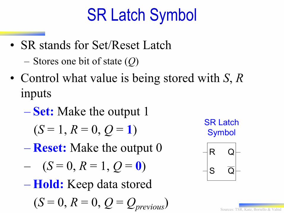
S
R Q
Q
SR Latch
Symbol
• SR stands for Set/Reset Latch
– Stores one bit of state (Q)
• Control what value is being stored with S, R
inputs
– Set: Make the output 1
(S = 1, R = 0, Q = 1)
– Reset: Make the output 0
– (S = 0, R = 1, Q = 0)
– Hold: Keep data stored
(S = 0, R = 0, Q = Qprevious)
• Must do something to avoid
invalid state (when S = R = 1)
SR Latch Symbol
Sources: TSR, Katz, Boriello & Vahid
8
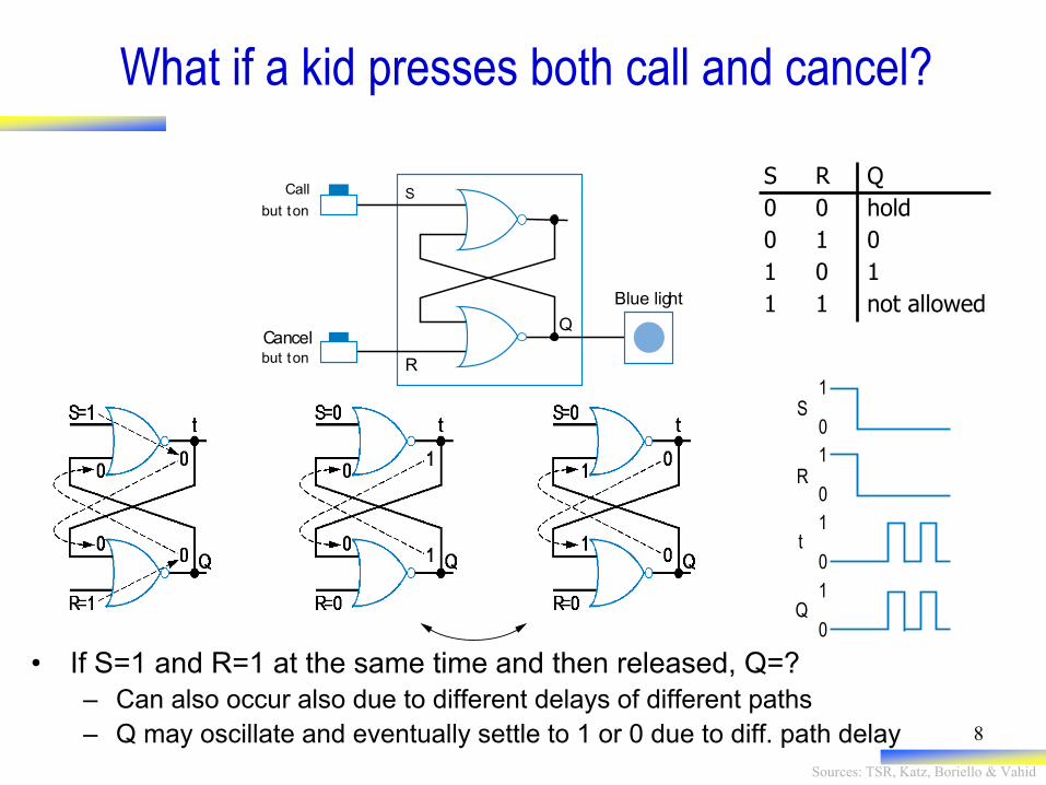
What if a kid presses both call and cancel?
• If S=1 and R=1 at the same time and then released, Q=?
– Can also occur also due to different delays of different paths
– Q may oscillate and eventually settle to 1 or 0 due to diff. path delay
0
1
0
1
0
1
0
1
S
R
Q
t
R
S
Q
C all
but t on
Blue lig h t
C an c el but t on
S R Q
0 0 hold
0 1 0
1 0 1
1 1 not allowed
Sources: TSR, Katz, Boriello & Vahid
9
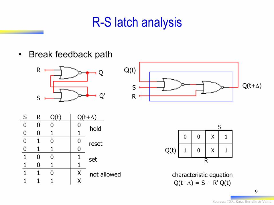
Q(t+)
R
S
Q(t)
S R Q(t) Q(t+)
0 0 0 0
0 0 1 1
0 1 0 0
0 1 1 0
1 0 0 1
1 0 1 1
1 1 0 X
1 1 1 X
hold
reset
set
not allowed characteristic equation
Q(t+) = S + R’ Q(t)
R-S latch analysis
• Break feedback path
R
S
Q
Q'
0 0
1 0
X 1
X 1 Q(t)
R
S
Sources: TSR, Katz, Boriello & Vahid
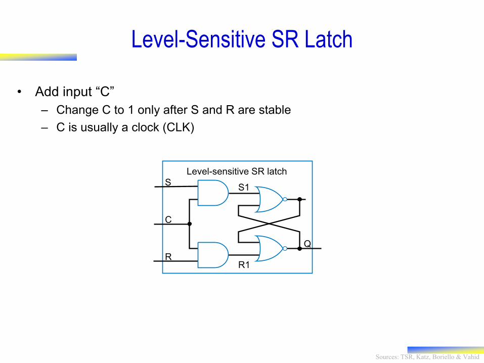
Level-Sensitive SR Latch
• Add input “C”
– Change C to 1 only after S and R are stable
– C is usually a clock (CLK)
R1
S1 S
C
R
Level-sensitive SR latch
Q
Sources: TSR, Katz, Boriello & Vahid
11
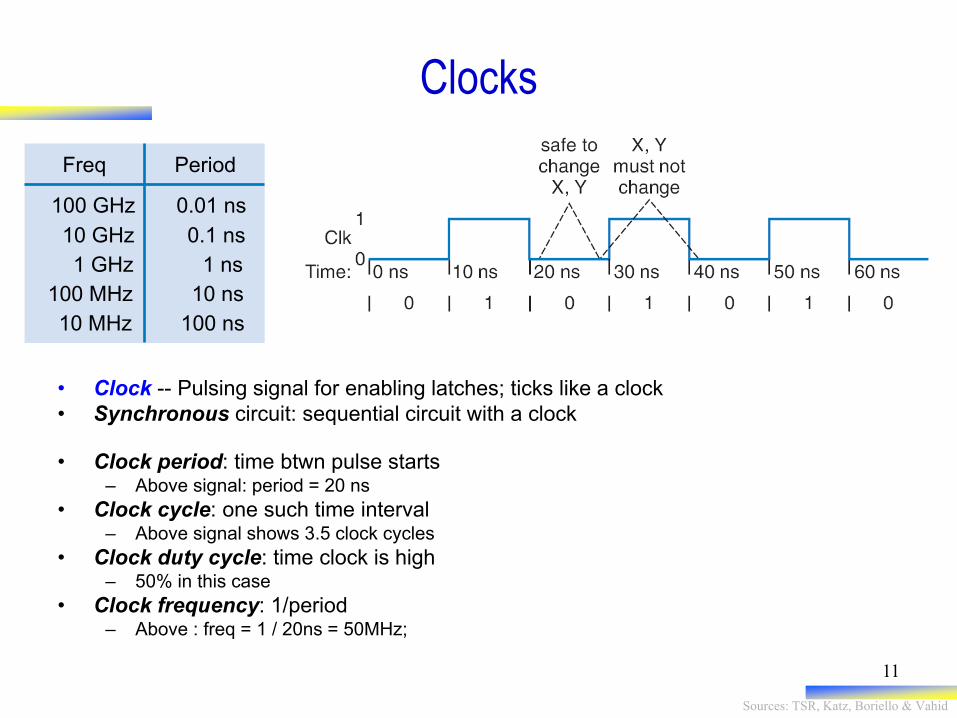
Clocks
• Clock -- Pulsing signal for enabling latches; ticks like a clock
• Synchronous circuit: sequential circuit with a clock
• Clock period: time btwn pulse starts – Above signal: period = 20 ns
• Clock cycle: one such time interval – Above signal shows 3.5 clock cycles
• Clock duty cycle: time clock is high – 50% in this case
• Clock frequency: 1/period – Above : freq = 1 / 20ns = 50MHz;
100 GHz
10 GHz
1 GHz
100 MHz
10 MHz
0.01 ns
0.1 ns
1 ns
10 ns
100 ns
Period Freq
Sources: TSR, Katz, Boriello & Vahid
12
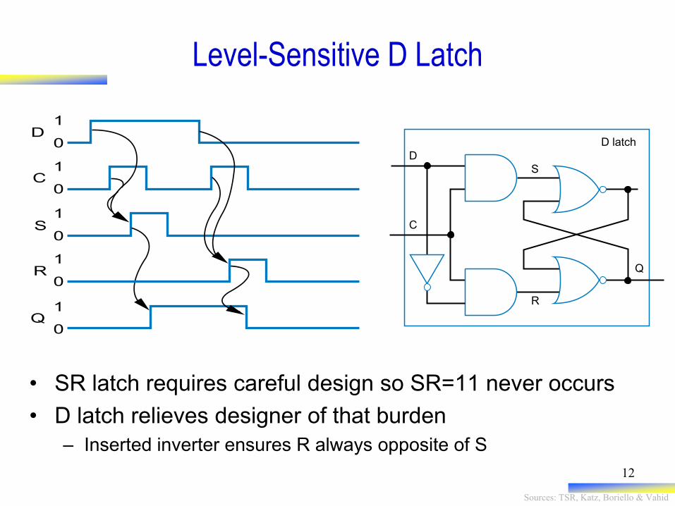
Level-Sensitive D Latch
• SR latch requires careful design so SR=11 never occurs
• D latch relieves designer of that burden
– Inserted inverter ensures R always opposite of S
R
S
D
C
D latch
Q
1
0D
C
S
R
Q
1
0
1
0
1
0
1
0
Sources: TSR, Katz, Boriello & Vahid
13
CSE140: Components and Design Techniques
for Digital Systems
Latches and flip-flops (cont.)
Tajana Simunic Rosing
Sources: Katz, Boriello & Vahid
Sources: TSR, Katz, Boriello & Vahid
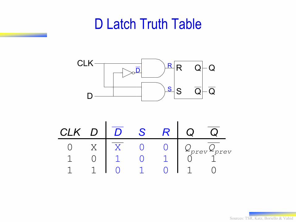
D Latch Truth Table
S
R Q
Q
Q
QD
CLKD
R
S
S R Q
0 0 Qprev
0 1 0
1 0 1
Q
1
0
CLK D
0 X
1 0
1 1
D
X
1
0
Qprev
Sources: TSR, Katz, Boriello & Vahid
D Latch
Symbol
CLK
D Q
Q
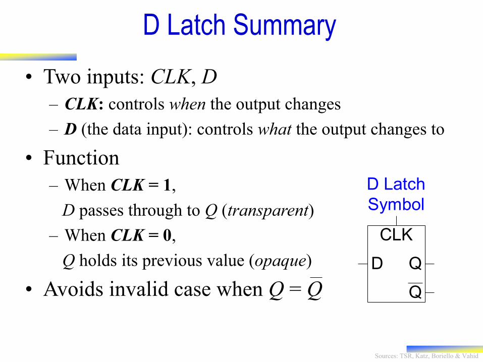
• Two inputs: CLK, D
– CLK: controls when the output changes
– D (the data input): controls what the output changes to
• Function
– When CLK = 1,
D passes through to Q (transparent)
– When CLK = 0,
Q holds its previous value (opaque)
• Avoids invalid case when Q = Q
D Latch Summary
Sources: TSR, Katz, Boriello & Vahid
16
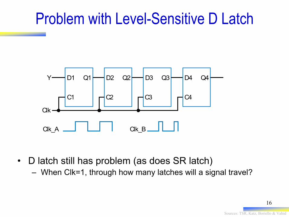
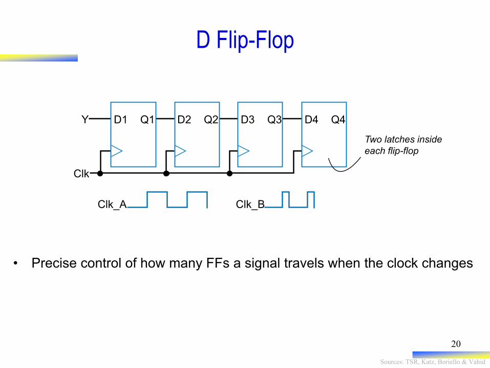
Problem with Level-Sensitive D Latch
• D latch still has problem (as does SR latch) – When Clk=1, through how many latches will a signal travel?
D1 Q1 D2 Q2 D3 Q3 D4
C4C3C2C1
Q4Y
Clk
Clk_A Clk_B
Sources: TSR, Katz, Boriello & Vahid
17
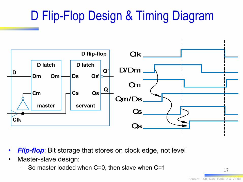
D Flip-Flop Design & Timing Diagram
• Flip-flop: Bit storage that stores on clock edge, not level
• Master-slave design:
– So master loaded when C=0, then slave when C=1
D latch
master
D latch
servant
D Dm Ds
Cs
Qm Q s ’
Qs Q
Q ’
C m
Clk
D flip-flop
Sources: TSR, Katz, Boriello & Vahid
CLK
D Q
Q
CLK
D Q
Q
Q
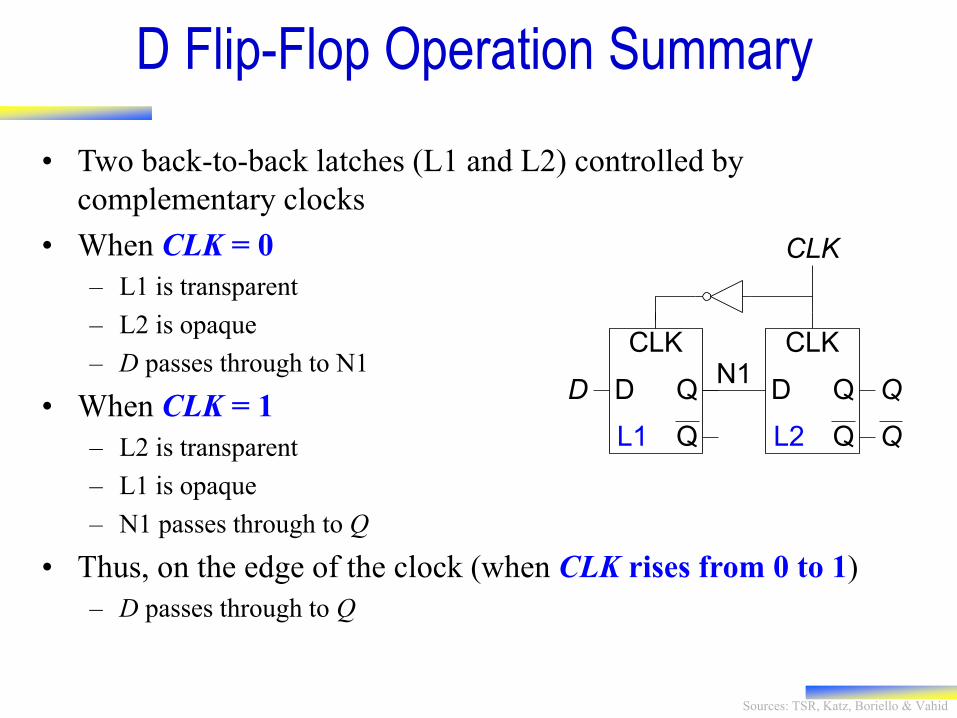
Q
DN1
CLK
L1 L2
• Two back-to-back latches (L1 and L2) controlled by
complementary clocks
• When CLK = 0
– L1 is transparent
– L2 is opaque
– D passes through to N1
• When CLK = 1
– L2 is transparent
– L1 is opaque
– N1 passes through to Q
• Thus, on the edge of the clock (when CLK rises from 0 to 1)
– D passes through to Q
D Flip-Flop Operation Summary
Sources: TSR, Katz, Boriello & Vahid
19
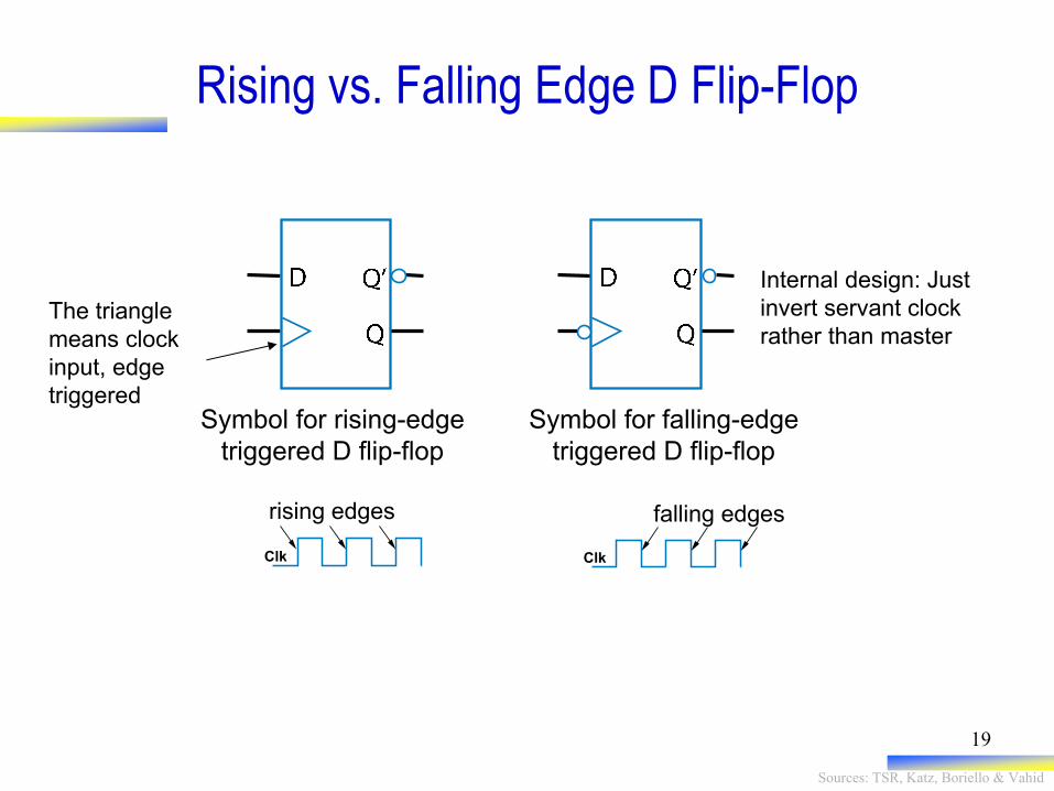
Rising vs. Falling Edge D Flip-Flop
Symbol for rising-edge
triggered D flip-flop
Symbol for falling-edge
triggered D flip-flop
Clk
rising edges
Clk
falling edges
Internal design: Just
invert servant clock
rather than master The triangle
means clock
input, edge
triggered
Sources: TSR, Katz, Boriello & Vahid
20
D Flip-Flop
• Precise control of how many FFs a signal travels when the clock changes
Two latches inside
each flip-flop
D1 Q1 D2 Q2 D3 Q3 D4 Q4 Y
Clk
Clk_A Clk_B
Sources: TSR, Katz, Boriello & Vahid
21
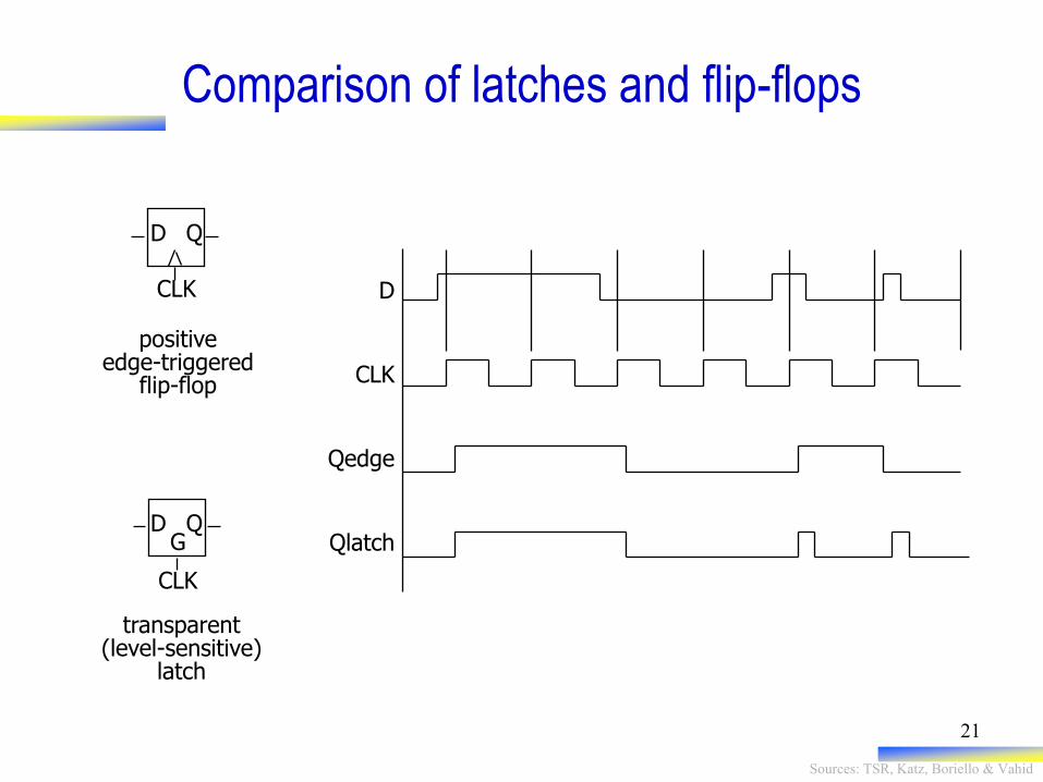
D Q
CLK
positive edge-triggered
flip-flop
D Q G
CLK
transparent (level-sensitive)
latch
D
CLK
Qedge
Qlatch
Comparison of latches and flip-flops

Sources: TSR, Katz, Boriello & Vahid
Internal
Circuit
D Q
CLKEN
DQ
0
1D Q
EN
Symbol
• Inputs: CLK, D, EN – The enable input (EN) controls when new data (D) is stored
• Function – EN = 1: D passes through to Q on the clock edge
– EN = 0: the flip-flop retains its previous state
Enabled Flip-Flops
Sources: TSR, Katz, Boriello & Vahid
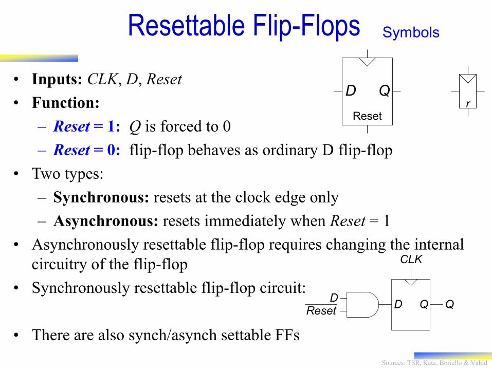
Symbols
D Q
Resetr
Resettable Flip-Flops
Internal
Circuit
D Q
CLK
DQ
Reset
• Inputs: CLK, D, Reset
• Function:
– Reset = 1: Q is forced to 0
– Reset = 0: flip-flop behaves as ordinary D flip-flop
• Two types:
– Synchronous: resets at the clock edge only
– Asynchronous: resets immediately when Reset = 1
• Asynchronously resettable flip-flop requires changing the internal
circuitry of the flip-flop
• Synchronously resettable flip-flop circuit:
• There are also synch/asynch settable FFs
Sources: TSR, Katz, Boriello & Vahid
24
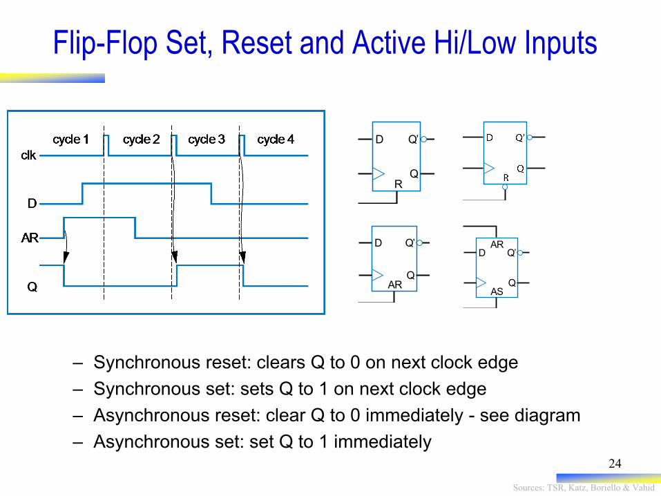
Flip-Flop Set, Reset and Active Hi/Low Inputs
– Synchronous reset: clears Q to 0 on next clock edge
– Synchronous set: sets Q to 1 on next clock edge
– Asynchronous reset: clear Q to 0 immediately - see diagram
– Asynchronous set: set Q to 1 immediately
D Q’
QR
Q’
AR
D
Q
Q’
AS
ARD
Q
Sources: TSR, Katz, Boriello & Vahid
25
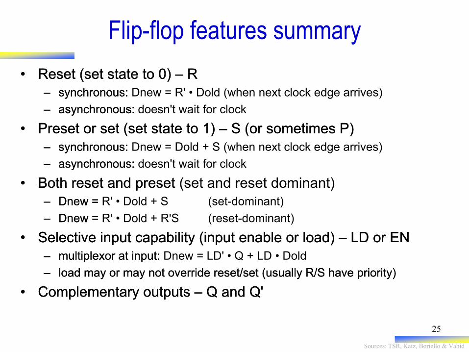
Flip-flop features summary
• Reset (set state to 0) – R
– synchronous:
– asynchronous:
• Preset or set (set state to 1) – S (or sometimes P)
– synchronous:
– asynchronous:
• Both reset and preset (set and reset dominant)
– Dnew =
– Dnew =
• Selective input capability (input enable or load) – LD or EN
– multiplexor at input:
– load may or may not override reset/set (usually R/S have priority)
• Complementary outputs – Q and Q'
• Reset (set state to 0) – R
– synchronous: Dnew = R' • Dold (when next clock edge arrives)
– asynchronous: doesn't wait for clock
• Preset or set (set state to 1) – S (or sometimes P)
– synchronous: Dnew = Dold + S (when next clock edge arrives)
– asynchronous: doesn't wait for clock
• Both reset and preset
– Dnew = R' • Dold + S (set-dominant)
– Dnew = R' • Dold + R'S (reset-dominant)
• Selective input capability (input enable or load) – LD or EN
– multiplexor at input: Dnew = LD' • Q + LD • Dold
– load may or may not override reset/set (usually R/S have priority)
• Complementary outputs – Q and Q'
Sources: TSR, Katz, Boriello & Vahid
26
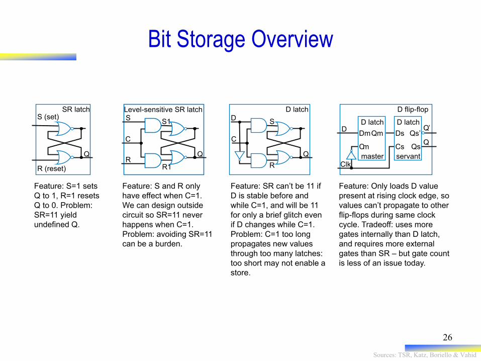
Bit Storage Overview
D flip-flop
D latch
master
D latch
servant
Dm Qm
C m
Ds D
Clk
Qs’
Cs Qs
Q ’
Q
S
R
D
Q
C
D latch
Feature: Only loads D value
present at rising clock edge, so
values can’t propagate to other
flip-flops during same clock
cycle. Tradeoff: uses more
gates internally than D latch,
and requires more external
gates than SR – but gate count
is less of an issue today.
Feature: SR can’t be 11 if
D is stable before and
while C=1, and will be 11
for only a brief glitch even
if D changes while C=1.
Problem: C=1 too long
propagates new values
through too many latches:
too short may not enable a
store.
S1
R1
S
Q
C
R
Level-sensitive SR latch
Feature: S and R only
have effect when C=1.
We can design outside
circuit so SR=11 never
happens when C=1.
Problem: avoiding SR=11
can be a burden.
R (reset)
S (set)
Q
SR latch
Feature: S=1 sets
Q to 1, R=1 resets
Q to 0. Problem:
SR=11 yield
undefined Q.
Sources: TSR, Katz, Boriello & Vahid
27
CSE140: Components and Design Techniques
for Digital Systems
Finite state machines
Tajana Simunic Rosing
Sources: Katz, Boriello & Vahid
Sources: TSR, Katz, Boriello & Vahid
28
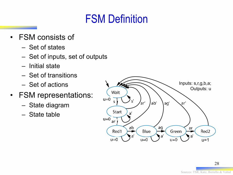
FSM Definition
• FSM consists of
– Set of states
– Set of inputs, set of outputs
– Initial state
– Set of transitions
– Set of actions
• FSM representations:
– State diagram
– State table
u=1
Inputs: s,r,g,b,a;
Outputs: u
Sources: TSR, Katz, Boriello & Vahid
29
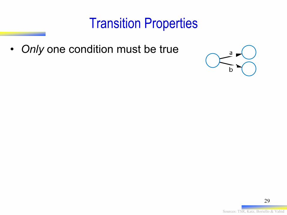
Transition Properties
• Only one condition must be true
Sources: TSR, Katz, Boriello & Vahid
30
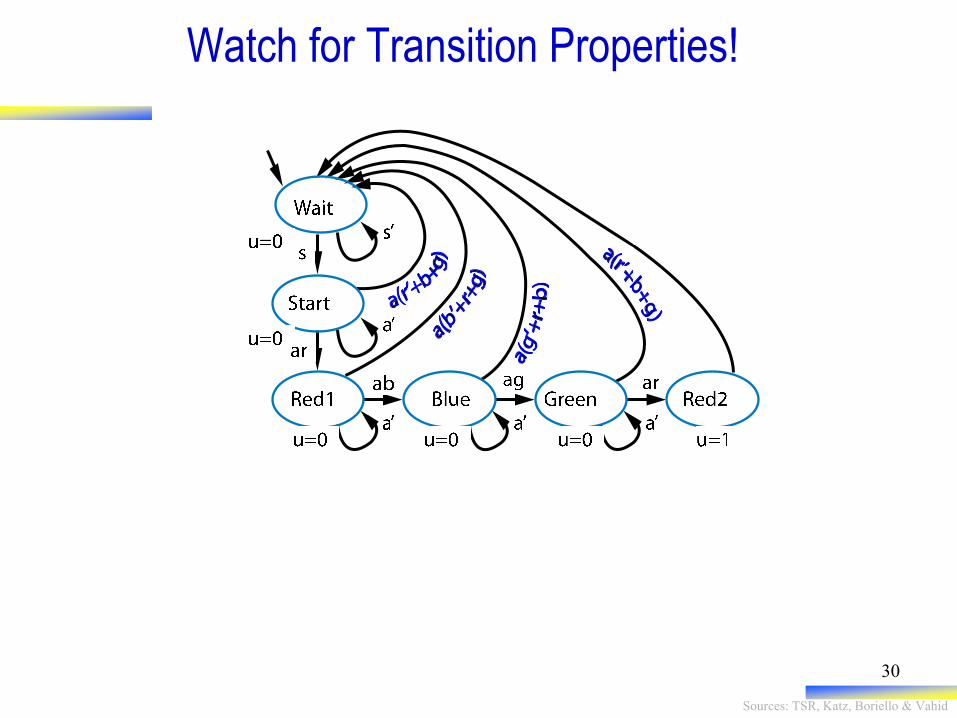
Watch for Transition Properties!
Sources: TSR, Katz, Boriello & Vahid
31
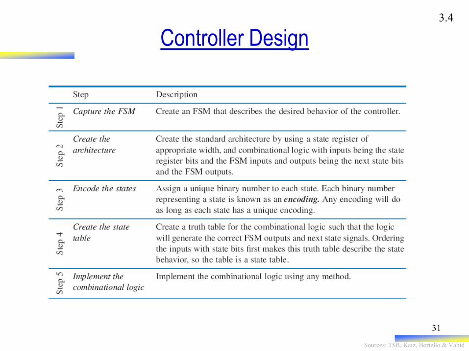
Controller Design 3.4
Sources: TSR, Katz, Boriello & Vahid
32
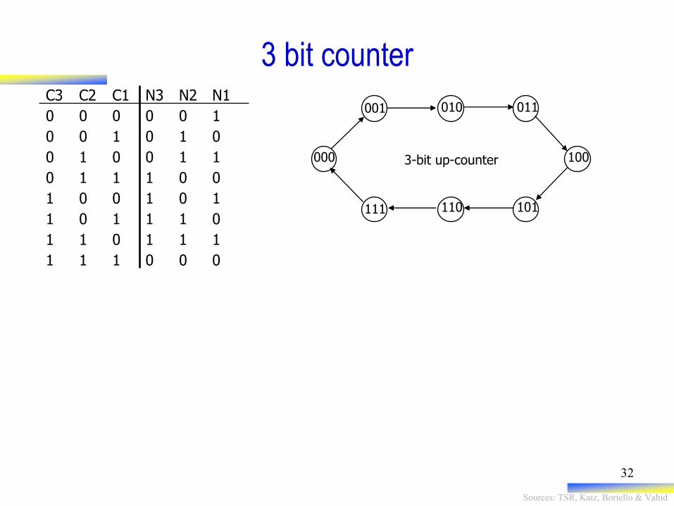
C3 C2 C1 N3 N2 N1
0 0 0 0 0 1
0 0 1 0 1 0
0 1 0 0 1 1
0 1 1 1 0 0
1 0 0 1 0 1
1 0 1 1 1 0
1 1 0 1 1 1
1 1 1 0 0 0
3 bit counter
010
100
110
011 001
000
101 111
3-bit up-counter

Sources: TSR, Katz, Boriello & Vahid
33
010
100
110
011 001
000
101 111
3-bit up-counter
How do we turn a state diagram into logic?
D Q D Q D Q
OUT1 OUT2 OUT3
CLK
"1"
Sources: TSR, Katz, Boriello & Vahid
34
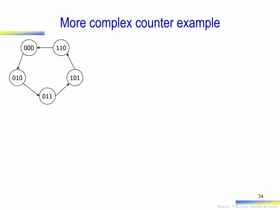
More complex counter example
010
000 110
101
011
Sources: TSR, Katz, Boriello & Vahid
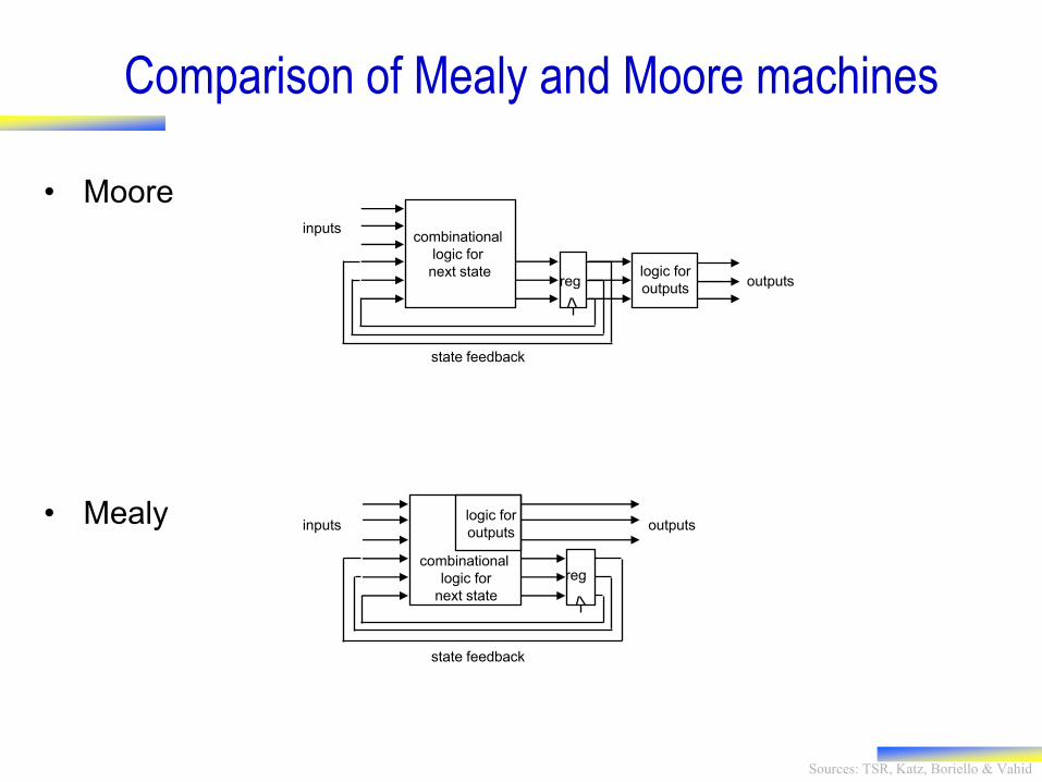
Comparison of Mealy and Moore machines
• Moore
• Mealy
state feedback
inputs
outputs reg
combinational
logic for
next state logic for
outputs
inputs outputs
state feedback
reg combinational
logic for
next state
logic for
outputs
Sources: TSR, Katz, Boriello & Vahid
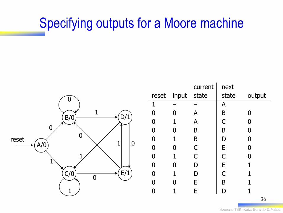
36
D/1
E/1
B/0
A/0
C/0
1
0
0
0
0
1
1
1
1
0
reset
current next
reset input state state output
1 – – A
0 0 A B 0
0 1 A C 0
0 0 B B 0
0 1 B D 0
0 0 C E 0
0 1 C C 0
0 0 D E 1
0 1 D C 1
0 0 E B 1
0 1 E D 1
Specifying outputs for a Moore machine
Sources: TSR, Katz, Boriello & Vahid
37
current next
reset input state state output
1 – – A 0
0 0 A B 0
0 1 A C 0
0 0 B B 0
0 1 B C 1
0 0 C B 1
0 1 C C 0
B
A
C
0/1
0/0
0/0
1/1
1/0
1/0
reset/0
Specifying outputs for a Mealy machine
Sources: TSR, Katz, Boriello & Vahid
38
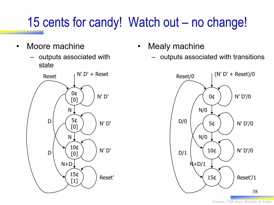
15 cents for candy! Watch out – no change!
• Moore machine
– outputs associated with
state
0¢ [0]
10¢ [0]
5¢ [0]
15¢ [1]
N’ D’ + Reset
D
D
N
N+D
N
N’ D’
Reset’
N’ D’
N’ D’
Reset
0¢
10¢
5¢
15¢
(N’ D’ + Reset)/0
D/0
D/1
N/0
N+D/1
N/0
N’ D’/0
Reset’/1
N’ D’/0
N’ D’/0
Reset/0
• Mealy machine
– outputs associated with transitions
Sources: TSR, Katz, Boriello & Vahid
39
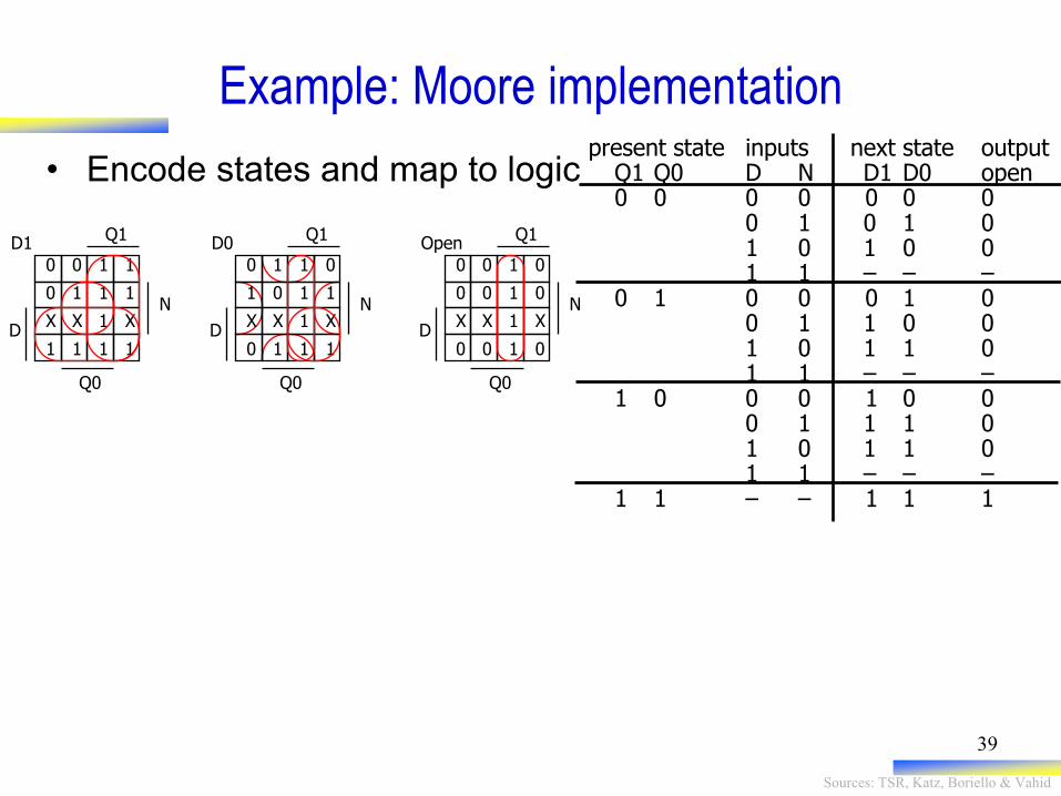
Example: Moore implementation
• Encode states and map to logic
0 0 1 1
0 1 1 1
X X 1 X
1 1 1 1
Q1 D1
Q0
N
D
0 1 1 0
1 0 1 1
X X 1 X
0 1 1 1
Q1 D0
Q0
N
D
0 0 1 0
0 0 1 0
X X 1 X
0 0 1 0
Q1 Open
Q0
N
D
present state inputs next state output Q1 Q0 D N D1 D0 open 0 0 0 0 0 0 0 0 1 0 1 0 1 0 1 0 0 1 1 – – – 0 1 0 0 0 1 0 0 1 1 0 0 1 0 1 1 0 1 1 – – – 1 0 0 0 1 0 0 0 1 1 1 0 1 0 1 1 0 1 1 – – – 1 1 – – 1 1 1
Sources: TSR, Katz, Boriello & Vahid
40
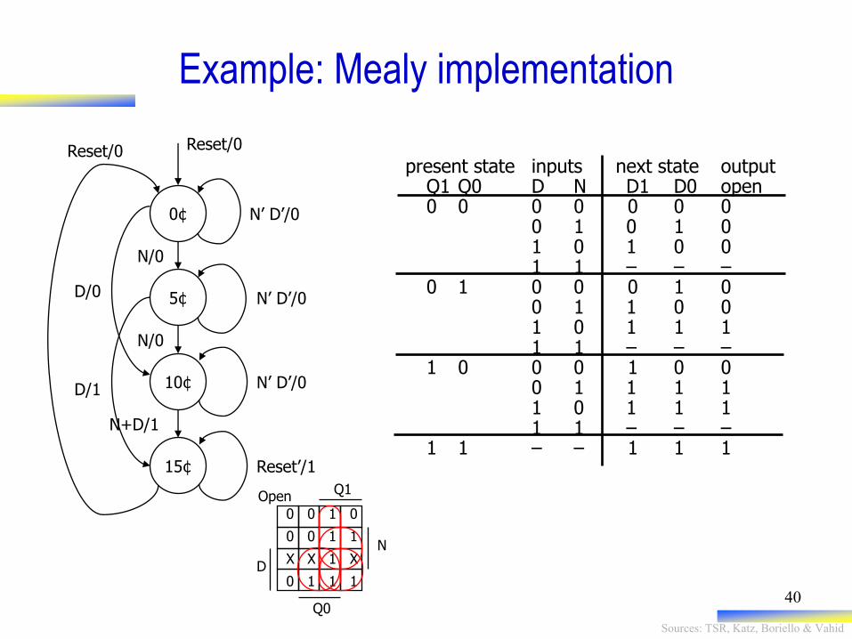
Example: Mealy implementation
0¢
10¢
5¢
15¢
Reset/0
D/0
D/1
N/0
N+D/1
N/0
N’ D’/0
Reset’/1
N’ D’/0
N’ D’/0
Reset/0 present state inputs next state output Q1 Q0 D N D1 D0 open 0 0 0 0 0 0 0 0 1 0 1 0 1 0 1 0 0 1 1 – – – 0 1 0 0 0 1 0 0 1 1 0 0 1 0 1 1 1 1 1 – – – 1 0 0 0 1 0 0 0 1 1 1 1 1 0 1 1 1 1 1 – – – 1 1 – – 1 1 1
0 0 1 0
0 0 1 1
X X 1 X
0 1 1 1
Q1 Open
Q0
N
D
Sources: TSR, Katz, Boriello & Vahid
41
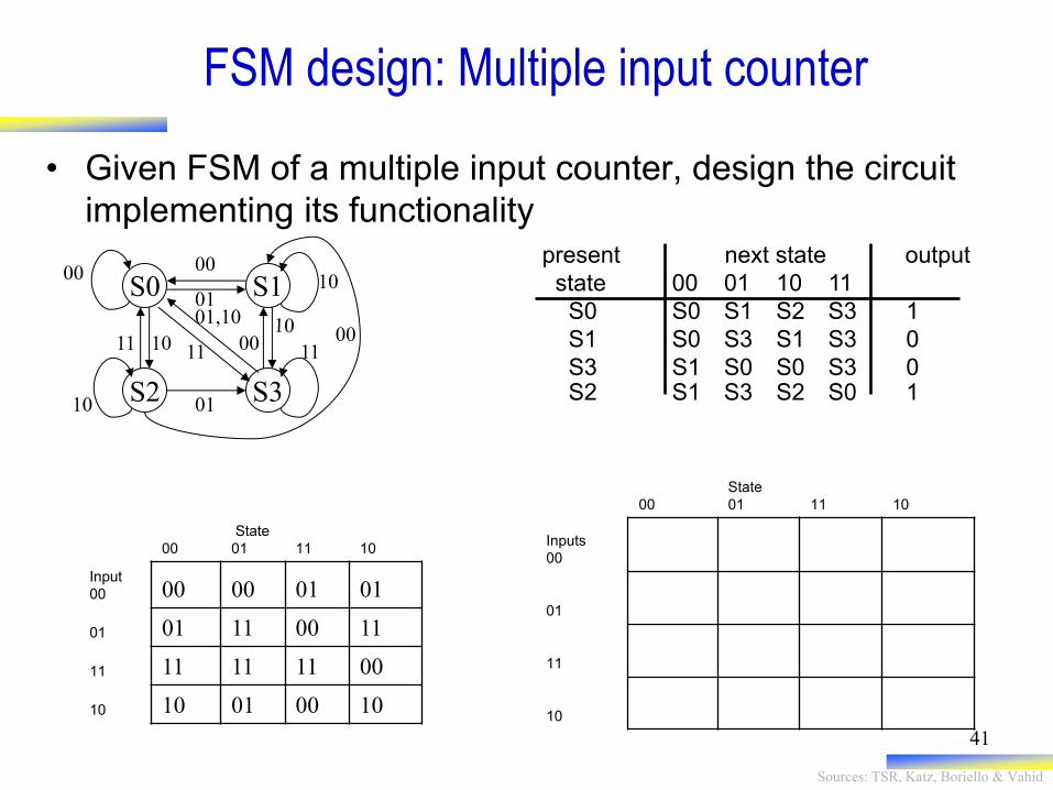
present next state output
state 00 01 10 11
S0 S0 S1 S2 S3 1
S1 S0 S3 S1 S3 0
S3 S1 S0 S0 S3 0 S2 S1 S3 S2 S0 1
FSM design: Multiple input counter
• Given FSM of a multiple input counter, design the circuit
implementing its functionality
S0 S1
S2 S3
00
00
01
10 11
10
01,10
10
11
01
00 11
00
00
State
01
11
10
Inputs
00
01
11
10
00
State
01
11
10
Input
00 00 00 01 01
01 01 11 00 11
11 11 11 11 00
10 10 01 00 10
Sources: TSR, Katz, Boriello & Vahid
42
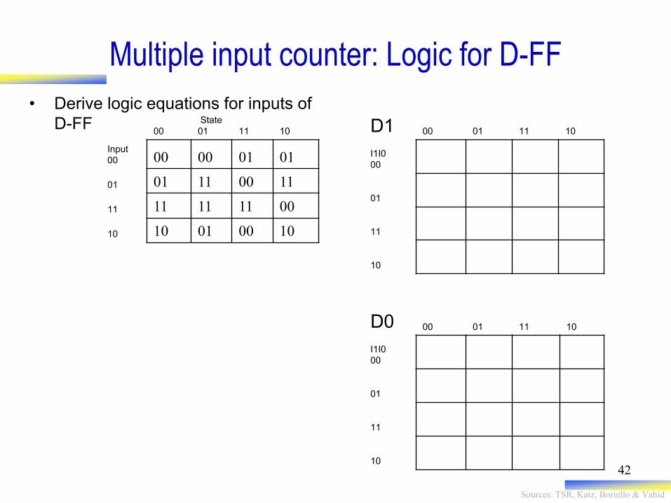
Multiple input counter: Logic for D-FF
• Derive logic equations for inputs of
D-FF D1 00
01
11
10
I1I0
00
01
11
10
D0 00
01
11
10
I1I0
00
01
11
10
00
State
01
11
10
Input
00 00 00 01 01
01 01 11 00 11
11 11 11 11 00
10 10 01 00 10
Sources: TSR, Katz, Boriello & Vahid
Unfactored FSM
Factored FSM
Controller
FSMTA
TB
LA
LB
PR
Mode
FSM
Lights
FSM
P
M
Controller
FSM
TA
TB
LA
LB
R
S0
LA: green
LB: red
S1
LA: yellow
LB: red
S3
LA: red
LB: yellow
S2
LA: red
LB: green
TA
TA
TB
TB
Reset
S4
LA: green
LB: red
S5
LA: yellow
LB: red
S7
LA: red
LB: yellow
S6
LA: red
LB: green
TA
TA
P
PP
P
P
P
R
R
R
R
R
P
RP
TA
P
TA
P
P
TA
R
TA
R
R
TB
RT
BR
S0
LA: green
LB: red
S1
LA: yellow
LB: red
S3
LA: red
LB: yellow
S2
LA: red
LB: green
TA
TA
M + TB
MTB
Reset
Lights FSM
S0
M: 0
S1
M: 1
PReset
P
Mode FSM
R
R
• Break complex FSMs into smaller interacting FSMs
Factoring State Machines
Sources: TSR, Katz, Boriello & Vahid
44
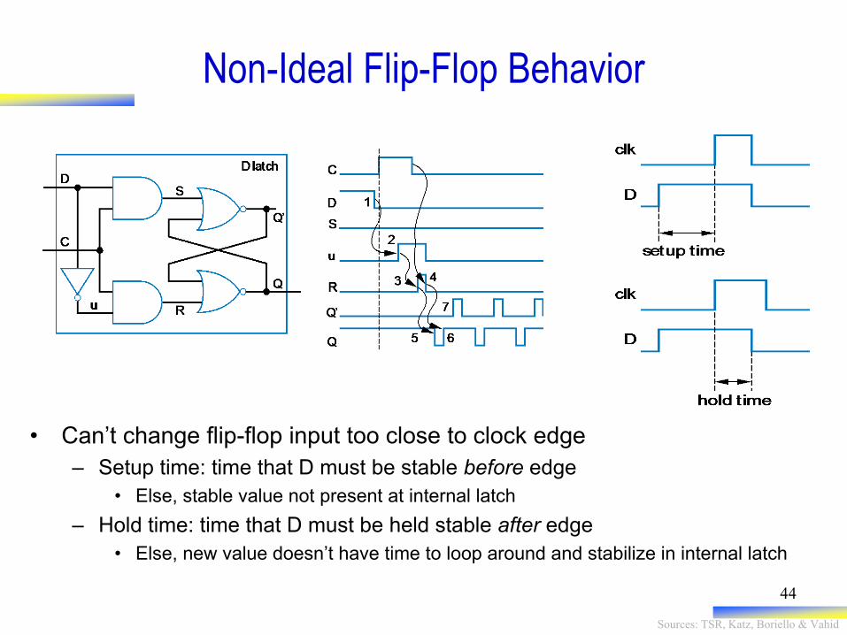
Non-Ideal Flip-Flop Behavior
• Can’t change flip-flop input too close to clock edge
– Setup time: time that D must be stable before edge
• Else, stable value not present at internal latch
– Hold time: time that D must be held stable after edge
• Else, new value doesn’t have time to loop around and stabilize in internal latch
Sources: TSR, Katz, Boriello & Vahid
45
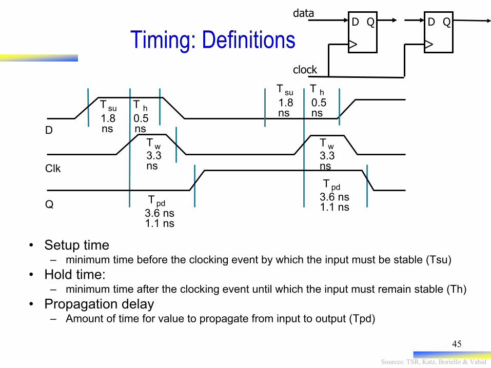
clock
data D Q D Q
Timing: Definitions
• Setup time – minimum time before the clocking event by which the input must be stable (Tsu)
• Hold time: – minimum time after the clocking event until which the input must remain stable (Th)
• Propagation delay – Amount of time for value to propagate from input to output (Tpd)
D
Clk
Q
T su
1.8 ns
T h
0.5 ns
T w
3.3 ns
T pd
3.6 ns 1.1 ns
T su
1.8 ns
T h
0.5 ns
T pd
3.6 ns 1.1 ns
T w
3.3 ns
Sources: TSR, Katz, Boriello & Vahid
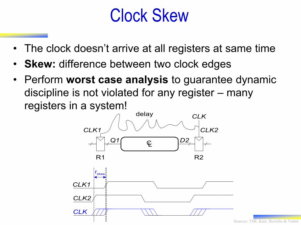
• The clock doesn’t arrive at all registers at same time
• Skew: difference between two clock edges
• Perform worst case analysis to guarantee dynamic
discipline is not violated for any register – many
registers in a system!
tskew
CLK1
CLK2
CL
CLK2CLK1
R1 R2
Q1 D2
CLKdelay
CLK
Clock Skew
Sources: TSR, Katz, Boriello & Vahid
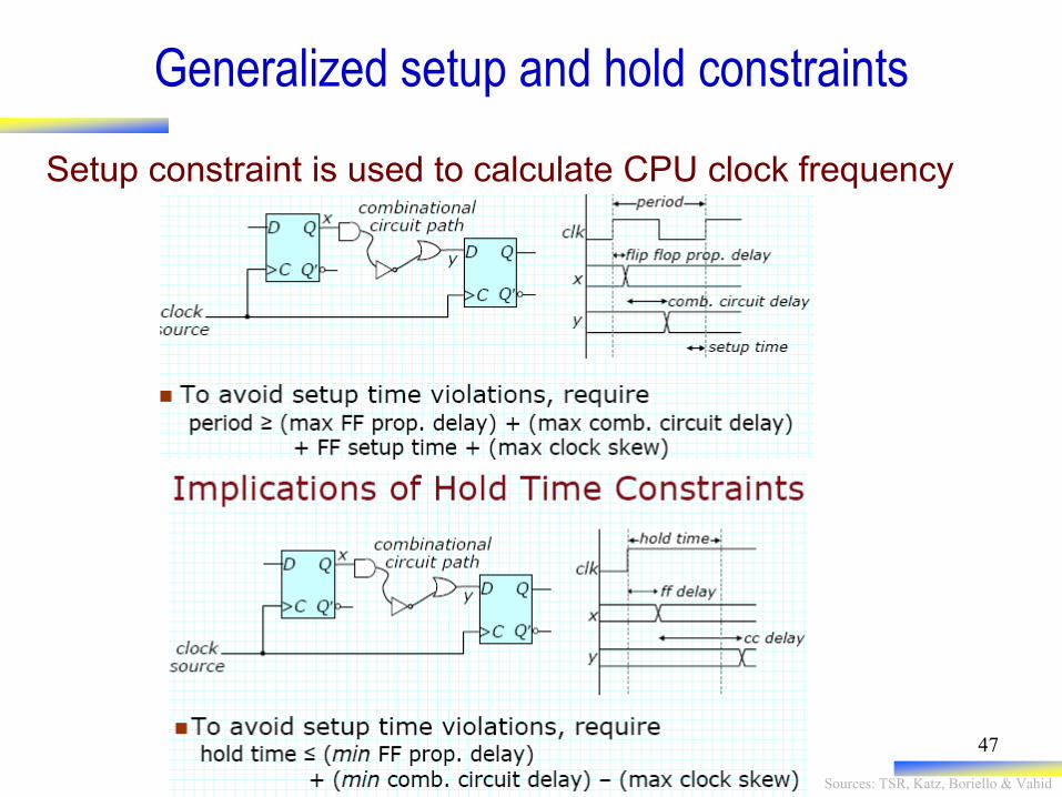
Generalized setup and hold constraints
Setup constraint is used to calculate CPU clock frequency
47
Sources: TSR, Katz, Boriello & Vahid
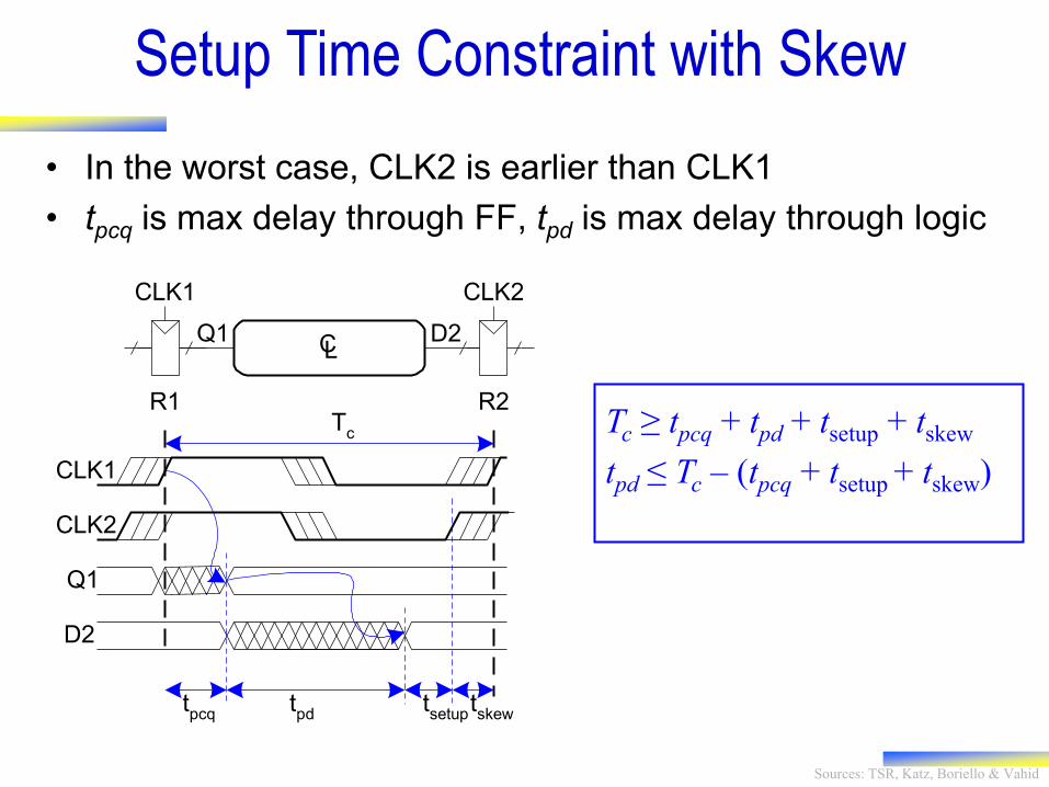
• In the worst case, CLK2 is earlier than CLK1
• tpcq is max delay through FF, tpd is max delay through logic
CLK1
Q1
D2
Tc
tpcq
tpd
tsetup
tskew
CL
CLK2CLK1
R1 R2
Q1 D2
CLK2
Tc ≥ tpcq + tpd + tsetup + tskew
tpd ≤ Tc – (tpcq + tsetup + tskew)
Setup Time Constraint with Skew
Sources: TSR, Katz, Boriello & Vahid
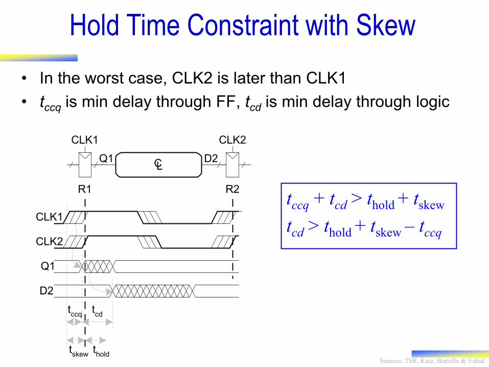
• In the worst case, CLK2 is later than CLK1
• tccq is min delay through FF, tcd is min delay through logic
tccq
tcd
thold
Q1
D2
tskew
CL
CLK2CLK1
R1 R2
Q1 D2
CLK2
CLK1
tccq + tcd > thold + tskew
tcd > thold + tskew – tccq
Hold Time Constraint with Skew
Sources: TSR, Katz, Boriello & Vahid
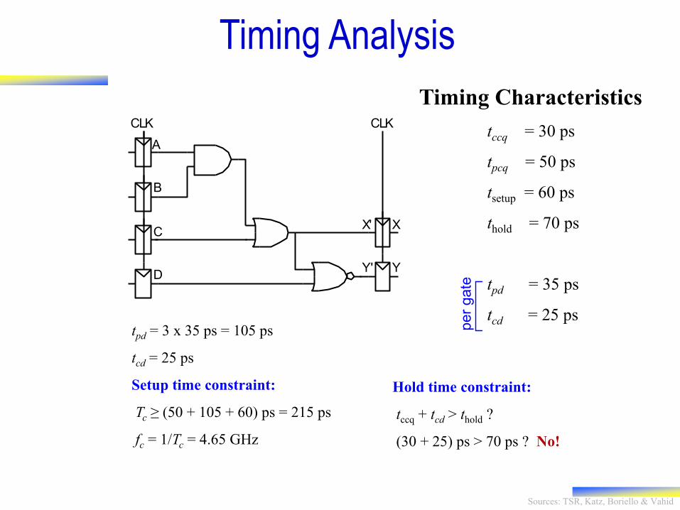
CLK CLK
A
B
C
D
X'
Y'
X
Y
per
gate
Timing Characteristics
tccq = 30 ps
tpcq = 50 ps
tsetup = 60 ps
thold = 70 ps
tpd = 35 ps
tcd = 25 ps tpd = 3 x 35 ps = 105 ps
tcd = 25 ps
Setup time constraint:
Tc ≥ (50 + 105 + 60) ps = 215 ps
fc = 1/Tc = 4.65 GHz
Hold time constraint:
tccq + tcd > thold ?
(30 + 25) ps > 70 ps ? No!
Timing Analysis
Sources: TSR, Katz, Boriello & Vahid
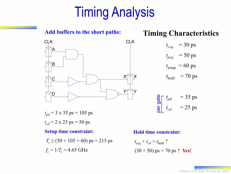
Timing Characteristics
tccq = 30 ps
tpcq = 50 ps
tsetup = 60 ps
thold = 70 ps
tpd = 35 ps
tcd = 25 ps tpd = 3 x 35 ps = 105 ps
tcd = 2 x 25 ps = 50 ps
Setup time constraint:
Tc ≥ (50 + 105 + 60) ps = 215 ps
fc = 1/Tc = 4.65 GHz
Hold time constraint:
tccq + tcd > thold ?
(30 + 50) ps > 70 ps ? Yes!
Timing Analysis
CLK CLK
A
B
C
D
X'
Y'
X
Y
Add buffers to the short paths:
per
gate
Sources: TSR, Katz, Boriello & Vahid
52
Timing Analysis
• Draw the timing diagram assuming:
– Tsu = 2 ns; Th = 1ns; Tprop = 3ns
– Period = 6ns, duty cycle 50%
Sources: TSR, Katz, Boriello & Vahid
53
Summary
• Finite State Machine definition
• Mealy vs. Moore FSM
• Design procedure for FSMs
1. Capture FSM
2. Encode the states
3. Create state table
4. Implement combinational logic for next states and output
Sources: TSR, Katz, Boriello & Vahid
Registers and Counters
54
Sources: TSR, Katz, Boriello & Vahid
55
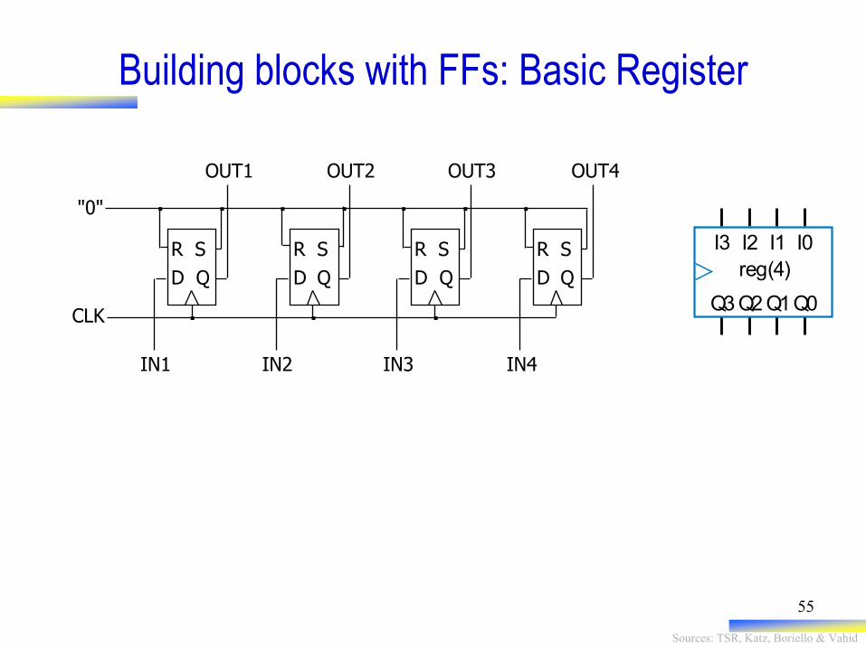
Building blocks with FFs: Basic Register
I3 I2 I1 I0
Q3 Q2 Q1Q0
reg(4)R S R S R S
D Q D Q D Q D Q
OUT1 OUT2 OUT3 OUT4
CLK
IN1 IN2 IN3 IN4
R S
"0"
Sources: TSR, Katz, Boriello & Vahid
56
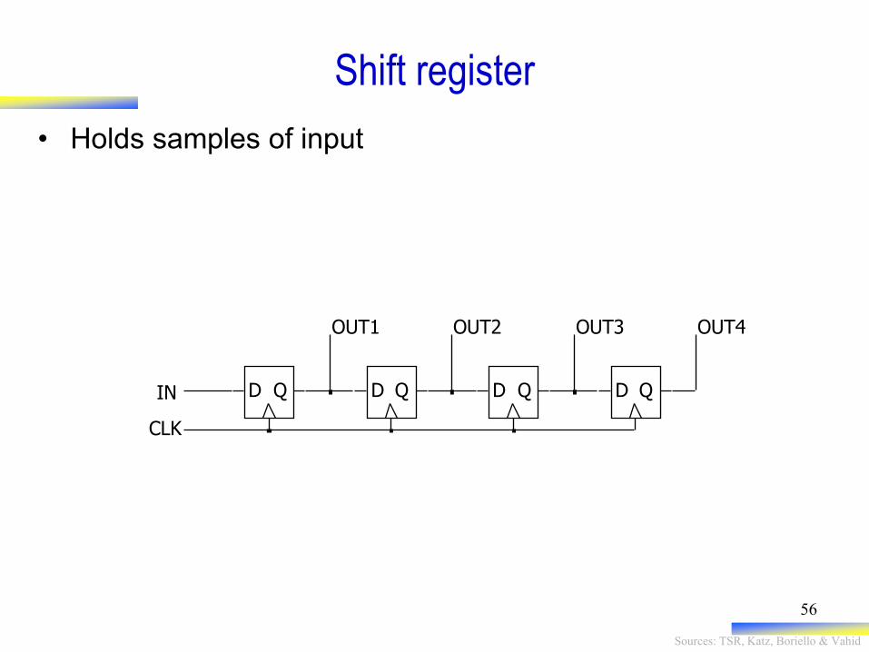
D Q D Q D Q D Q IN
OUT1 OUT2 OUT3 OUT4
CLK
Shift register
• Holds samples of input
Sources: TSR, Katz, Boriello & Vahid
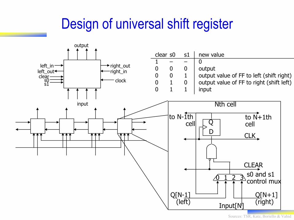
Nth cell
D
Q
CLK
Q[N-1] (left)
Q[N+1] (right)
Input[N]
to N-1th cell
to N+1th cell
clear s0 s1 new value 1 – – 0 0 0 0 output
0 0 1 output value of FF to left (shift right) 0 1 0 output value of FF to right (shift left) 0 1 1 input
Design of universal shift register
s0 and s1 control mux
0 1 2 3
CLEAR
left_in left_out
right_out
clear right_in
output
input
s0 s1
clock
Sources: TSR, Katz, Boriello & Vahid
58
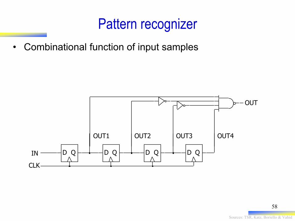
D Q D Q D Q D Q IN
OUT1 OUT2 OUT3 OUT4
CLK
OUT
Pattern recognizer
• Combinational function of input samples
Sources: TSR, Katz, Boriello & Vahid
59
Counters
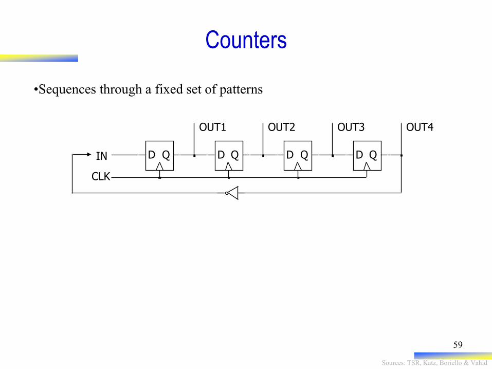
D Q D Q D Q D Q IN
OUT1 OUT2 OUT3 OUT4
CLK
•Sequences through a fixed set of patterns
Sources: TSR, Katz, Boriello & Vahid
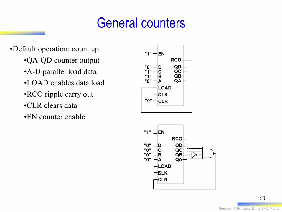
60
EN
D C B A
LOAD
CLK
CLR
RCO
QD QC QB QA
"1"
"0" "0" "0" "0"
"0"
EN
D C B A
LOAD
CLK
CLR
RCO
QD QC QB QA
"1"
"0" "1" "1" "0"
General counters
•Default operation: count up
•QA-QD counter output
•A-D parallel load data
•LOAD enables data load
•RCO ripple carry out
•CLR clears data
•EN counter enable