cse140: components and design techniques for digital...
TRANSCRIPT

Sources: TSR, Katz, Boriello, Vahid, Perkowski
CSE140: Components and Design Techniques
for Digital Systems
High-Level Finite State Machines & Memory
Tajana Simunic Rosing

Sources: TSR, Katz, Boriello, Vahid, Perkowski
Class Status, Updates & Plans
• What we covered:– Combinational logic
– Latches, FFs
– Registers, counters, FSMs & timing
– HLSM & timing
• Plan for today:– HLSM examples, memory
• Upcoming deadlines:– HW#7 assigned, due Thursday
• The last HW for the quarter!!!!
• Prof. office hour – Moves from Thursday to Friday at 12-1pm just this week

Sources: TSR, Katz, Boriello, Vahid, Perkowski
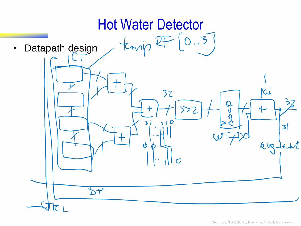
Hot Water Detector
Create an alarm system that sets alarm=1 when the average
temperature of four consecutive samples CT meets or
exceeds a threshold WT. Signal clr=1 disables the alarm.
Sources: TSR, Katz, Boriello, Vahid, Perkowski
Hot Water Detector
• Datapath design

Sources: TSR, Katz, Boriello, Vahid, Perkowski
CSE140: Components and Design Techniques
for Digital Systems
Memory
Tajana Simunic Rosing

Sources: TSR, Katz, Boriello, Vahid, Perkowski
Memory: basic concepts
• Stores large number of bits
– m x n: m words of n bits each
– k = Log2(m) address input signals
– or m = 2^k words
– e.g., 4,096 x 8 memory:
• 32,768 bits
• 12 address input signals
• 8 input/output data signals
• Memory access
– r/w: selects read or write
– enable: read or write only when asserted
– multiport: multiple accesses to different
locations simultaneously
m × n memory
…
…
n bits per word
mw
ord
s
enable
2k × n read and write
memory
A0…
r/w
…
Q0Qn-1
Ak-1
memory external view

Sources: TSR, Katz, Boriello, Vahid, Perkowski
Composing Memory – Wider Words
• Making memory words wider
– Easy – just place memories side-by-side until desired width obtained
– Share address/control lines, concatenate data lines
– Example: Compose 1024x8 ROMs into 1024x32 ROM
1024x32ROM
1024x8ROM
data
addr
endata
8 8
32
8
10
10
en
addr
data(31..0)
1024x8ROM
addr
endata
1024x8ROM
addr
endata
1024x8ROM
addr
endata
8
addr
en
data

Sources: TSR, Katz, Boriello, Vahid, Perkowski
Composing Memory – More Words
• Creating memory with more words
– Combine memories until the number of desired words is achieved
– Use decoder to select
– Example: Compose 1024x8 memories into 2048x8 memory
• More words and wider words – first make enough words, then widen
Province 2
Province 1
1024x8ROM
addr
en data
1024x8ROM
addr
en data
0 0 0 0 0 0 0 0 0 0 0
0 0 0 0 0 0 0 0 0 0 1
0 0 0 0 0 0 0 0 0 1 0
0 1 1 1 1 1 1 1 1 1 0
0 1 1 1 1 1 1 1 1 1 1
1 0 0 0 0 0 0 0 0 0 0
1 0 0 0 0 0 0 0 0 0 1
1 0 0 0 0 0 0 0 0 1 0
1 1 1 1 1 1 1 1 1 1 0
1 1 1 1 1 1 1 1 1 1 1
a0a10a9a8
a10 just chooses
which memory
to access
2048x8ROM
data
8
11
11
1024x8ROM
addr
en data
8
1024x8ROM
addr
en data
8
a9..a0
a10 d0
d1
en
addr 1x2dcdi0
e
addr
en

Sources: TSR, Katz, Boriello, Vahid, Perkowski
Write ability/ storage permanence
• Traditional ROM/RAM
– ROM
• read only, bits stored
without power
– RAM
• read and write, lose stored
bits without power
• Distinctions blurred
– Advanced ROMs can be
written to
• e.g., EEPROM
– Advanced RAMs can hold
bits without power
• e.g., NVRAM Write ability and storage permanence of memories,
showing relative degrees along each axis (not to scale).
External
programmer
OR in-system,
block-oriented
writes, 1,000s
of cycles
Battery
life (10
years)
Write
ability
EPROM
Mask-programmed ROM
EEPROM FLASH
NVRAM
SRAM/DRAM
Sto
rage
per
man
ence
Nonvolatile
In-system
programmable
Ideal memory
OTP ROM
During
fabrication
only
External
programmer,
1,000s
of cycles
External
programmer,
one time only
External
programmer
OR in-system,
1,000s
of cycles
In-system, fast
writes,
unlimited
cycles
Near
zero
Tens of
years
Life of
product
Sources: TSR, Katz, Boriello, Vahid, Perkowski
Comparing RAM
• Register file
– Fastest
– But biggest size
• SRAM
– Fast (e.g. 10ns)
– More compact than register file
• DRAM
– Slowest (e.g. 20ns)
• And refreshing takes time
– But very compact
– Different technology for large caps.
Data
W
Data'
SRAM
Data
W
DRAM
R S R S R S
D Q D Q D Q D Q
OUT1 OUT2 OUT3 OUT4
CLK
IN1 IN2 IN3 IN4
R S
REGISTER FILE

Sources: TSR, Katz, Boriello, Vahid, Perkowski
Caches and CPUs
• Servers: Level 1 (L1),L2 &L3 cache on chip
• Embedded: L1, L2 on chip
Raspberry Pi 3Intel Xeon Server

Sources: TSR, Katz, Boriello, Vahid, Perkowski
Raspberry Pi 3 – Memory Architecture
• Broadcom BCM2837 SoC
– CPU: Quad-core Cortex-A53: L1 and L2 cache
– GPU: VideoCore IV® Processor: exclusive memory system
– Main Memory: 1GB RAM : Shared by CPU and GPU
VideoCore IVARM Cortex-A53
Used by CPU Used by GPU
L2 Cache
I Cache D Cache
L1 Cache (per core)
Main Memory
L2 Cache
I Cache
Uniform cache
Textual Memory Unit
Per slice
BC
M2
83
7 S
oC

Sources: TSR, Katz, Boriello, Vahid, Perkowski
ARM v8 memory hierarchy (in RPi3)
Tightly coupled memory (TCM) = SRAM organized as main memory
CPUs chip

Sources: TSR, Katz, Boriello, Vahid, Perkowski
Random Access Memory (RAM)
• RAM – Readable and writable memory
– Logically the same as register file
• RAM just one port; register file two or more
– RAM vs. register file
• RAM is larger
• RAM stores bits using a bit storage vs. FFs
• RAM implemented on a chip in a square –
keeps longest wires (hence delay) short32
10data
addr
rw
en
1024× 32RAM
32
4
32
4
W_data
W_addr
W_en
R_data
R_addr
R_en16×32
register file
Register file
RAM block symbol

Sources: TSR, Katz, Boriello, Vahid, Perkowski
RAM Internal Structure
• Similar internal structure as register file
– Decoder enables appropriate word based on address inputs
– rw controls whether cell is written or read
– Let’s see what’s inside each RAM cell
32
10data
addr
rw
en
1024x32RAM
addr0addr1
addr(A-1)
clk
enrw
Let A = log2M
to all cells
wdata(N-1)
rdata(N-1)
wdata(N-2)
rdata(N-2)
wdata0
rdata0
bit storageblock(aka “cell”)
word
word
RAM cell
wordenable
wordenable
rw
data cell
data
a0a1
d0
d1
d(M-1)
a(A-1)
e
AxMdecoder
enable

Sources: TSR, Katz, Boriello, Vahid, Perkowski
Static RAM (SRAM) - writing
• “Static” RAM cell
– 6 transistors (recall inverter is 2 transistors)
– Writing this cell
• word enable input comes from decoder
• When 0, value d loops around inverters
– That loop is where a bit stays stored
• When 1, the data bit value enters the loop
– data is the bit to be stored in this cell
– data’ enters on other side
– Example shows a “1” being written into cell
SRAM celldata data’
d’dcell
0wordenable
1
1
1
0
0
32
10data
addr
rw
en
1024x32RAM
SRAM celldata data’
d
wordenable

Sources: TSR, Katz, Boriello, Vahid, Perkowski
Static RAM (SRAM) - reading
• “Static” RAM cell - reading
– When rw set to read, the RAM logic sets both data and data’ to 1
– The stored bit d will pull either the left line or the right bit down slightly below 1
– “Sense amplifiers” detect which side is slightly pulled down
SRAM cell
32
10data
addr
rw
en
1024x32RAM
data data’
d
1
1 1
wordenable
To sense amplifiers
1 0
1 <1
Sources: TSR, Katz, Boriello, Vahid, Perkowski
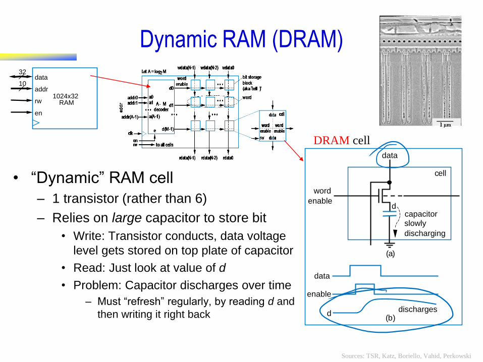
Dynamic RAM (DRAM)
• “Dynamic” RAM cell
– 1 transistor (rather than 6)
– Relies on large capacitor to store bit
• Write: Transistor conducts, data voltage
level gets stored on top plate of capacitor
• Read: Just look at value of d
• Problem: Capacitor discharges over time
– Must “refresh” regularly, by reading d and
then writing it right back
DRAM cell
32
10data
addr
rw
en
1024x32RAM
word
enable
data
cell
(a)
(b)
data
enable
ddischarges
dcapacitorslowly
discharging

Sources: TSR, Katz, Boriello, Vahid, Perkowski
Comparing Memory Types
• Register file
– Fastest
– But biggest size
• SRAM
– Fast
– More compact than register file
• DRAM
– Slowest
• And refreshing takes time
– But very compact
– Different technology for large caps.
MxN Memoryimplemented as a:
registerfile
SRAM
DRAM
Size comparison for the same
number of bits (not to scale)
Data
W
Data'
SRAM
Data
W
DRAM
R S R S R S
D Q D Q D Q D Q
OUT1 OUT2 OUT3 OUT4
CLK
IN1 IN2 IN3 IN4
R S
REGISTER FILE

Sources: TSR, Katz, Boriello, Vahid, Perkowski
RAM Example: Digital Sound Recorder
• Behavior
– Record: Digitize sound, store as series of 4096 12-bit digital values in RAM
• We’ll use a 4096x16 RAM (12-bit wide RAM not common)
– Play back later from RAM
wire
speaker
microphone
wireanalog-to-
digitalconverter
digital-to-analog
converter
ad_ld da_ld
Rrw RenRa12
16
processor
ad_buf
dat
a
add
r
rw en
4096× 16RAM
Sources: TSR, Katz, Boriello, Vahid, Perkowski
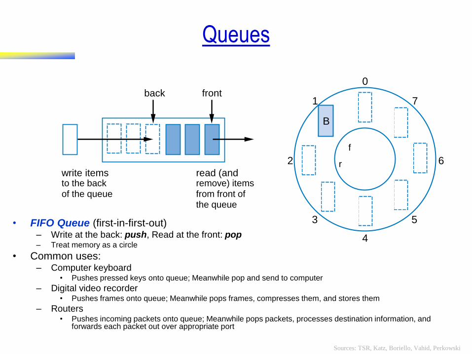
Queues
• FIFO Queue (first-in-first-out)– Write at the back: push, Read at the front: pop– Treat memory as a circle
• Common uses:– Computer keyboard
• Pushes pressed keys onto queue; Meanwhile pop and send to computer
– Digital video recorder• Pushes frames onto queue; Meanwhile pops frames, compresses them, and stores them
– Routers• Pushes incoming packets onto queue; Meanwhile pops packets, processes destination information, and
forwards each packet out over appropriate port
frontback
write itemsto the backof the queue
read (andremove) itemsfrom front ofthe queue
B
1 7
2 6
3 5
4
0
f
r
r

Sources: TSR, Katz, Boriello, Vahid, Perkowski
Queues
• Two conditions have front=rear need FSM to detect:
– Full: No pushes until a pop
– Empty: No pops until a push
• Use Register file for storage
• Implement Rear and frontwith up counters:
– rear as RF’s write address, front as read address

Sources: TSR, Katz, Boriello, Vahid, Perkowski
HLSM with memory example:
Fibonacci Lookup Table
• Design a lookup table 256 x 256 bit that stores Fibonacci #s:
– Fn = 0 if n = 0, 1 if n = 1, Fn-1 + Fn-2 otherwise (n<256)

Sources: TSR, Katz, Boriello, Vahid, Perkowski
Fibonacci
datapath
Sources: TSR, Katz, Boriello, Vahid, Perkowski
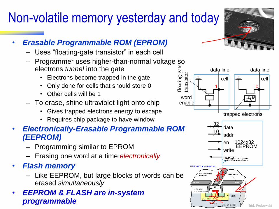
Non-volatile memory yesterday and today
• Erasable Programmable ROM (EPROM)
– Uses “floating-gate transistor” in each cell
– Programmer uses higher-than-normal voltage so electrons tunnel into the gate
• Electrons become trapped in the gate
• Only done for cells that should store 0
• Other cells will be 1
– To erase, shine ultraviolet light onto chip
• Gives trapped electrons energy to escape
• Requires chip package to have window
• Electronically-Erasable Programmable ROM (EEPROM)
– Programming similar to EPROM
– Erasing one word at a time electronically
• Flash memory
– Like EEPROM, but large blocks of words can be erased simultaneously
• EEPROM & FLASH are in-system programmable
cell cell
wordenable
data line data line
eÐeÐ
trapped electrons
01
flo
atin
g-g
ate
tran
sist
or
32
10data
addr
en
write
busy
1024x32EEPROM

Sources: TSR, Katz, Boriello, Vahid, Perkowski
ROM Example: Digital Telephone Answering Machine
• Record the outgoing announcement
– When rec=1, record digitized sound in locations 0 to 4095
– When play=1, play those stored sounds to digital-to-analog converter
analog-to-digital
converterdigital-to-
analogconverterad_ld
da_ld
Rrw Rener buRa12
16
processor
ad_buf
busy
4096x16 Flash
rec
playrecord
microphone speaker
“We’re not home.”

Sources: TSR, Katz, Boriello, Vahid, Perkowski
ROM Example: Digital Telephone Answering Machine
• High-level state machine
– Once rec=1, begin erasing flash by setting er=1
– Wait for flash to finish erasing by waiting for bu=0
– Execute loop that sets local register a from 0 to 4095, reading
analog-to-digital converter and writing to flash for each a
da rw en
analog-to-digital
converterdigital-to-
analogconverterad_ld
da_ld
Rrw Ren er buRa12
16
processor
ad_buf
4096x16 Flash
recplayrecord
microphone speaker
T
er=0
bu
bu’
er=1
rec
S
Local register: a (13 bits)
a=4096
a<4096
U
V
ad_ld=1ad_buf=1Ra=aRrw=1Ren=1a=a+1
a=0

Sources: TSR, Katz, Boriello, Vahid, Perkowski
Non-volatile memory going forward
• A new class of data storage/memory devices
• Emerging NVMs have exciting features:– Non-volatile like Flash ( ~ 10 years)
– Fast access times (~ SRAM)
– High density (~ DRAM)
• NVM blurs the distinction between – Memory (fast, expensive, volatile) &
– Storage (slow, cheap, non-volatile)
• Key issues:– Slow writes, low endurance, costly and complex manufacturing
http://www.vikingtechnology.com/uploads/nv_whitepaper.pdf
Sources: TSR, Katz, Boriello, Vahid, Perkowski
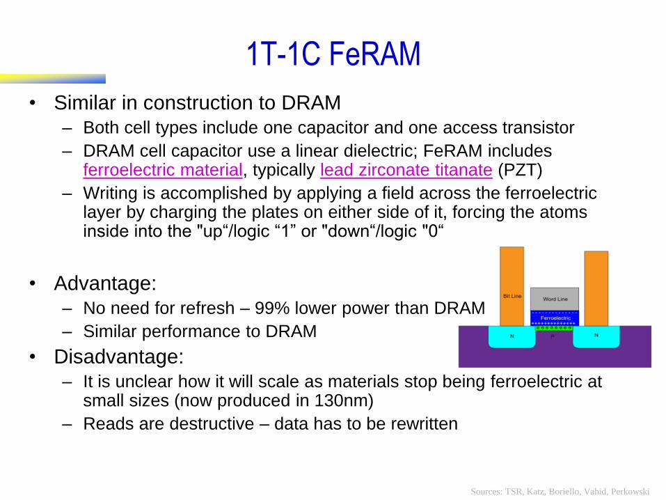
1T-1C FeRAM
• Similar in construction to DRAM
– Both cell types include one capacitor and one access transistor
– DRAM cell capacitor use a linear dielectric; FeRAM includes ferroelectric material, typically lead zirconate titanate (PZT)
– Writing is accomplished by applying a field across the ferroelectric layer by charging the plates on either side of it, forcing the atoms inside into the "up“/logic “1” or "down“/logic "0“
• Advantage:
– No need for refresh – 99% lower power than DRAM
– Similar performance to DRAM
• Disadvantage:
– It is unclear how it will scale as materials stop being ferroelectric at small sizes (now produced in 130nm)
– Reads are destructive – data has to be rewritten

Sources: TSR, Katz, Boriello, Vahid, Perkowski
STT-RAM: Spin-Transfer Torque RAM
• The spin torque direction of electrons to flip a bit in a magnetic
tunneling junction (MTJ)
(a) Structure of MTJ
(b) Parallel: bit 0 (low resistance)
(c) Anti-Parallel: bit 1 (high resistance)
• Advantages:
• High endurance & fast reads
• Disadvantages:
• Write energy: large current needed
to reorient the magnetization for
most commercial applications.;
• Asymmetric write: Writing a “1”
needs much more time and energy
than writing a “0”

Sources: TSR, Katz, Boriello, Vahid, Perkowski
Domain Wall Memory (DWM)
• Similar to STT-RAM structure
• Advantage:
– needs only one tunneling barrier and fixed layer → area savings
• Disadvantages:
– complexity of design, read/write delay due to sequential access
Ferromagnetic tape
Free LayerDomain Wall
Domain Fixed Layer Extra Domains
MTJ

Sources: TSR, Katz, Boriello, Vahid, Perkowski
Shift-based DWM
• Writes by shifting data of one of the two fixed layers with
the desirable direction comp
• Advantage: faster writes than a traditional DWM
• Disadvantage: cost and manufacturing complexity
1-bit DWM is fast Multi-bit DWM is area efficient,
but needs extra latency for shifting
39
Polarized direction

Sources: TSR, Katz, Boriello, Vahid, Perkowski
PCM: Phase Change Memory
Phase Change Memory (PCM)– Flips a bit by changing the state of material
– Crystalline (SET) and amorphous (RESET) phase
PCM Cell Phases
PCM Operation
Advantages:
– better scalability than other
emerging technologies
Disadvantages:
– Slow writes
– Low endurance (107 writes)
Candidate for DRAM replacement

Sources: TSR, Katz, Boriello, Vahid, Perkowski
ReRAM: Resistive RAM
• Two types: Access-based (1T-1R) and crossbar ReRAM
(1T-nR)
• Access-based ReRAM (1T-1R)
– A dielectric, which is normally an insulator, can conduct with
sufficiently high voltage
• Advantage:
– Very fast reads and writes ~ 20ns
– Very high density
• Disadvantage:
– Limited endurance (105 writes)

Sources: TSR, Katz, Boriello, Vahid, Perkowski
Crossbar ReRAM
Crossbar ReRAM (1T-nR)
Advantage:
Highly scalable
Can be implemented at the top of the chip with in 3D architecture
Very low energy consumption
Low cost (possible replacement for Flash)
Disadvantage:
Much slower than 1T-1R ~us

Sources: TSR, Katz, Boriello, Vahid, Perkowski
Crossbar RRAM Applications
https://www.crossbar-inc.com/assets/resource/presentation/FMS2014-Slides-RRAM-in-IoT.pdf
Crossbar 1T-nR 1T-1R
Sources: TSR, Katz, Boriello, Vahid, Perkowski
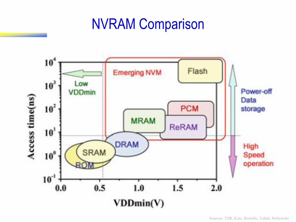
NVRAM Comparison
Sources: TSR, Katz, Boriello, Vahid, Perkowski
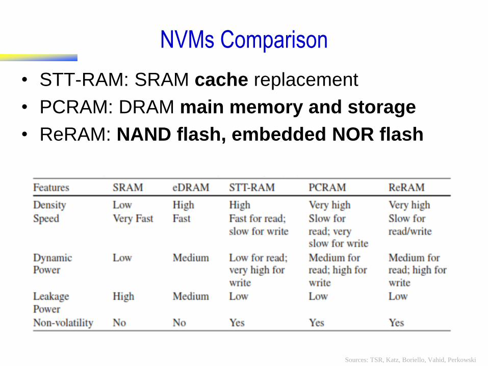
NVMs Comparison
• STT-RAM: SRAM cache replacement
• PCRAM: DRAM main memory and storage
• ReRAM: NAND flash, embedded NOR flash

Sources: TSR, Katz, Boriello, Vahid, Perkowski
Summary
• Memory hierarchy
– Needs: speed, low power, predictable
• Cache design
– Mapping, replacement & write policies
• Memory types
– ROM vs RAM vs NVM
• NVM
– Many new technologies that are still maturing
– Excellent target for big data and energy-efficient applications