control strategies for high power four-leg …
TRANSCRIPT

CONTROL STRATEGIES FOR HIGH POWER
FOUR-LEG VOLTAGE SOURCE INVERTERS
Robert A. Gannett
Thesis submitted to the Faculty of the Virginia Polytechnic Institute and State University
in partial fulfillment of the requirements for the degree of
MASTER OF SCIENCE in
Electrical Engineering
APPROVED:
Dushan Boroyevich, Chairman
Jason Lai Dan Y. Chen
July 30, 2001
Blacksburg, Virginia
Keywords: Voltage Source Inverter (VSI), synchronous frame control, current control,
unbalance load, non-linear load
Copyright 2001, Robert A. Gannett

Robert Gannett ABSTRACT
- ii -
Control Strategies for High Power Four-Leg Voltage Source Inverters
by
Robert A. Gannett
Dushan Boroyevich, Chairman
Electrical Engineering
ABSTRACT
In recent decades there has been a rapidly growing demand for high quality,
uninterrupted power. In light of this fact, this study has addressed some of the causes of
poor power quality and control strategies to ensure a high performance level in inverter-
fed power systems. In particular, specific loading conditions present interesting
challenges to inverter-fed, high power systems. No-load, unbalanced loading, and non-
linear loading each have unique characteristics that negatively influence the performance
of the Voltage Source Inverter (VSI). Ideal, infinitely stiff power systems are
uninfluenced by loading conditions; however, realistic systems, with finite output
impedances, encounter stability issues, unbalanced phase voltage, and harmonic
distortion. Each of the loading conditions is presented in detail with a proposed control
strategy in order to ensure superior inverter performance. Simulation results are
presented for a 90 kVA, 400 Hz VSI under challenging loading conditions to demonstrate
the merits of the proposed control strategies.
Unloaded or lightly loaded conditions can cause instabilities in inverter-fed power
systems, because of the lightly damped characteristic of the output filter. An inner
current loop is demonstrated to damp the filter poles at light load and therefore enable an
increase in the control bandwidth by an order of magnitude. Unbalanced loading causes
unequal phase currents, and consequently negative sequence and zero sequence (in four-
wire systems) distortion. A proposed control strategy based on synchronous and
stationary frame controllers is shown to reduce the phase voltage unbalance from 4.2% to

Robert Gannett ABSTRACT
- iii -
0.23% for a 100%-100%-85% load imbalance over fundamental positive sequence
control alone. Non-linear loads draw harmonic currents, and likewise cause harmonic
distortion in power systems. A proposed harmonic control scheme is demonstrated to
achieve near steady state errors for the low order harmonics due to non-linear loads. In
particular, the THD is reduced from 22.3% to 5.2% for full three-phase diode rectifier
loading, and from 11.3% to 1.5% for full balanced single-phase diode rectifier loading,
over fundamental control alone.

Robert Gannett ACKNOWLEDGEMENTS
- iv -
ACKNOWLEDGEMENTS
I would like to express my appreciation for my advisor, Dr. Dushan Boroyevich.
Dr. Boroyevich is deeply devoted to his students, and without his assistance, completing
this thesis certainly would not have been possible for me. First, I would like to thank Dr.
Boroyevich for introducing me to the exciting field of power electronics and for bringing
me into the CPES family. Second, I would like to thank him helping me through the
five-year B.S./M.S. on a timely schedule, while still challenging me every step of the
way. Dr. Boroyevich has given me a truly invaluable experience during my time at
CPES for which I am greatly indebted.
I would like to thank my other committee members, Dr. Jason Lai and Dr. Dan
Chen. Dr. Lai’s and Dr. Chen’s undergraduate courses first stimulated my interests in
electronics and are undoubtedly the reason for my continued education in the field. I
wish to thank Dr. Chen for his graduate courses that have given me real-world knowledge
that will be exceptionally helpful in my future career in industry. I would also like to
thank Dr. Lai for the opportunities with the Future Energy Challenge Team, which has
given me valuable practical engineering experience.
I would like to thank Trish Rose, Teresa Shaw, Suzanne Graham, Elizabeth
Tranter, Lesli Farmer, Bob Martin, Steve Chen, and all of the other CPES staff. They
make our work here at CPES possible.
One of the extraordinary things about CPES is the large pool of knowledge that
exists simply within the student base in the lab, and the willingness of those students to
share and aid their colleagues. I would especially like to thank my team members on the
AESS project, Erik Hertz, Dan Cochrane, Carl Tinsley, and Cory Papenfuss. They made
my job as project leader easy and made the long hours in the lab much more enjoyable.
There are several other students at CPES that I would like to thank. Heath Kouns
has truly been a pleasure to work with. He is a wonderful person and is always there to
help his fellow students regardless of his busy schedule. Dengming Peng helped me
through the difficult task of taking over as a project leader in a topic with which I had

Robert Gannett ACKNOWLEDGEMENTS
- v -
very little familiarity. I wish to thank my other friends at CPES, Troy Nergaard, Tom
Shearer, Jeremy Ferrell, Jerry Francis, and Len Leslie, who have made my experience at
CPES more than just academic. I would also like to thank all of my friends outside of
CPES for reminding me, every now and then, that there is more to life than just graduate
school.
I thank John Sozio for his assistance in all aspects of the research that has lead to
this thesis.
Most importantly, I would like to thank my parents for everything they have done
for me. They have pushed me throughout my academic career, and I certainly owe all of
my success to their loving support and guidance. I would also like to thank Nikki for her
love and strength throughout my graduate studies.
The research reported in this thesis was sponsored by the Office of Naval
Research and funded under grant number N000140010610. This work made use of ERC
Shared Facilities supported by the National Science Foundation under Award Number
EEC-9731677.

Robert Gannett TABLE OF CONTENTS
- vi -
TABLE OF CONTENTS
ABSTRACT ...................................................................................................................... II
ACKNOWLEDGEMENTS............................................................................................IV
TABLE OF CONTENTS................................................................................................VI
LIST OF FIGURES ........................................................................................................IX
LIST OF TABLES ...................................................................................................... XIII
1 INTRODUCTION ...................................................................................................... 1
1.1 APPLICATIONS FOR HIGH POWER INVERTERS ......................................................... 1
1.2 POWER QUALITY GUIDELINES AND STANDARDS .................................................... 3
1.2.1 Commercial Guidelines................................................................................... 4
1.2.2 Aircraft Standards........................................................................................... 6
1.3 HIGH POWER INVERTER CHALLENGES.................................................................... 8
1.3.1 Low Inverter Switching Frequencies............................................................... 8
1.3.2 Digital Delays ................................................................................................. 8
1.3.3 No-load Stability Concerns ........................................................................... 12
1.3.4 Unbalanced and Distorting Loads ................................................................ 13
1.4 400 HZ SYSTEMS .................................................................................................. 14
1.4.1 Applications................................................................................................... 14
1.4.2 Implications for Control Design ................................................................... 15
1.5 VOLTAGE SOURCE INVERTER UNDER STUDY ....................................................... 16
1.5.1 Inverter Switching Model .............................................................................. 16
1.5.2 Inverter Average Model ................................................................................ 17
1.6 OBJECTIVES .......................................................................................................... 19
2 NO-LOAD CONDITIONS ...................................................................................... 21
2.1 STABILITY ISSUES ................................................................................................. 21
2.1.1 Open Loop Plant Transfer Functions ........................................................... 21

Robert Gannett TABLE OF CONTENTS
- vii -
2.1.2 Analysis of Plant Transfer Functions............................................................ 28
2.2 NO-LOAD CONTROL DESIGN ................................................................................ 28
2.2.1 Conventional Voltage Loop Control ............................................................. 28
2.2.2 Inner Current Loop Control.......................................................................... 31
2.2.3 No-Load Control Summary ........................................................................... 41
2.3 CROSS-CHANNEL COUPLING................................................................................. 42
2.3.1 Cross-Coupling Transfer Functions ............................................................. 43
2.3.2 Advantages of Decoupling ............................................................................ 44
2.3.3 Decoupling Strategies ................................................................................... 45
2.3.4 Cross-Channel Coupling with Inner Current Loop ...................................... 52
2.3.5 Cross-Channel Coupling Summary............................................................... 53
2.4 NO-LOAD CONTROL SUMMARY............................................................................ 54
3 UNBALANCED LOADING CONDITIONS......................................................... 55
3.1 UNBALANCED LOAD IMPACT ON INVERTERS ........................................................ 55
3.1.1 Unbalanced Three-Phase Variable Representations .................................... 55
3.1.2 Implications for Control................................................................................ 57
3.1.3 Steady State DQO-Channel Solutions........................................................... 57
3.2 CONVENTIONAL SOLUTIONS ................................................................................. 59
3.2.1 Extending Controller Bandwidth .................................................................. 59
3.2.2 Load Current Feedforward Control.............................................................. 59
3.3 PROPOSED SOLUTION............................................................................................ 65
3.3.1 Motivations.................................................................................................... 65
3.3.2 Negative Sequence Controllers in Three-Leg Inverters................................ 66
3.3.3 Negative and Zero Sequence Controllers in Four-Leg Inverters.................. 66
3.4 UNBALANCED LOAD CONTROL SUMMARY ........................................................... 77
4 NON-LINEAR LOADING CONDITIONS ........................................................... 80
4.1 NON-LINEAR LOAD IMPACT ON INVERTERS.......................................................... 80
4.1.1 Three-Phase Diode Rectifiers ....................................................................... 80
4.1.2 Single-Phase Diode Rectifiers....................................................................... 83
4.2 CONVENTIONAL SOLUTIONS ................................................................................. 86

Robert Gannett TABLE OF CONTENTS
- viii -
4.2.1 Passive Filtering ........................................................................................... 86
4.2.2 Assistant Inverter and Active Filtering ......................................................... 87
4.2.3 Parallel Inverter Operation .......................................................................... 89
4.3 PROPOSED SOLUTION............................................................................................ 90
4.3.1 Motivations.................................................................................................... 90
4.3.2 Selective Harmonic Elimination in Three-Leg Inverters .............................. 91
4.3.3 Selective Harmonic Elimination in Four-Leg Inverters................................ 92
4.4 SUMMARY OF NON-LINEAR LOADING SOLUTIONS.............................................. 106
5 CONCLUSIONS AND FUTURE RESEARCH .................................................. 108
5.1 CONCLUSIONS..................................................................................................... 108
5.2 DIRECTION OF FUTURE RESEARCH...................................................................... 109
APPENDIX A PARK’S TRANSFORMATION...................................................... 111
APPENDIX B SYMMETRICAL DECOMPOSITION.......................................... 114
APPENDIX C LOAD CHARACTERIZATION..................................................... 116
C.1 THREE-PHASE DIODE RECTIFIER ........................................................................ 116
C.2 SINGLE-PHASE DIODE RECTIFIER ....................................................................... 121
REFERENCES.............................................................................................................. 126
VITA............................................................................................................................... 129

Robert Gannett LIST OF FIGURES
- ix -
LIST OF FIGURES
Figure 1.1 Block diagram of inverter preferred UPS system............................................. 2
Figure 1.2 Maximum voltage distortion for military aircraft power systems [11] ............ 7
Figure 1.3 Loop gain Bode diagrams before (-) and after (--) addition of control loop
time delay ................................................................................................................... 10
Figure 1.4 Basic system model including ideal time delay.............................................. 10
Figure 1.5 Origins of digital delay time length ................................................................ 12
Figure 1.6 Loop gain Bode diagrams at full load (-) and light load (--) .......................... 13
Figure 1.7 Schematic of the switching model of a four-leg inverter................................ 17
Figure 1.8 Four-leg inverter average model in dqo coordinates ...................................... 19
Figure 2.1 DQO channel average model including parasitic resistances......................... 23
Figure 2.2 Bode plots of the plant control to output transfer functions for the d- and q-
channels (-) and the o-channel (--) ............................................................................. 24
Figure 2.3 Bode plots of the control to inductor current transfer functions for the d- and
q-channels (-) and the o-channel (--) .......................................................................... 26
Figure 2.4 Bode plots of the control to output transfer functions with coupling terms for
the d- and q-channels (-) and o-channel (--) ............................................................... 27
Figure 2.5 Bode plots of the control to inductor current transfer functions with coupling
terms for the d- and q-channels (-) and o-channel (--) ............................................... 27
Figure 2.6 Bode plots of the loop gain containing integral voltage loop compensation for
the d- and q-channels (-) and the o-channel (--) ......................................................... 30
Figure 2.7 Closed loop inverter model containing integral compensation for each channel
.................................................................................................................................... 30
Figure 2.8 Nested Control Loops ..................................................................................... 32
Figure 2.9 System model including inner and outer control loops .................................. 33
Figure 2.10 Inner current loop gain Bode diagrams for the d- and q-channels (-) and the
o-channel (--) .............................................................................................................. 36
Figure 2.11 Bode diagrams of the closed inner current loop reference to output transfer
function for the d- and q-channels (-) and the o-channel (--), .................................... 36
Figure 2.12 Transfer function utilizing complex zeros .................................................... 37

Robert Gannett LIST OF FIGURES
- x -
Figure 2.13 Inner current loop gain Bode diagrams for the d- and q-channels (-) and the
o-channel (--) with modeled delay and complex zero compensation......................... 38
Figure 2.14 Closed loop inverter model with inner and outer control loops ................... 39
Figure 2.15 Voltage loop gain Bode plots for the d- and q-channels (-) and the o-channel
(--)............................................................................................................................... 40
Figure 2.16 Open loop d-channel control to output (-) and cross-coupling (--) transfer
functions ..................................................................................................................... 44
Figure 2.17 Open loop d-channel control to output transfer function with (-) and without
(--) the cross-channel coupling terms ......................................................................... 45
Figure 2.18 D- and q-channel models including the decoupling terms ........................... 46
Figure 2.19 D-channel control to output (-) and cross-coupling (--) transfer functions
with decoupling terms added...................................................................................... 47
Figure 2.20 Open loop d-channel control to output (-) and cross-coupling (--) transfer
functions with L-C adjustment ................................................................................... 49
Figure 2.21 State-space system with observer [21].......................................................... 51
Figure 2.22 D-channel control to output (-) and cross-coupling (--) transfer functions
with inductor voltage and capacitor current decoupling strategy............................... 51
Figure 2.23 D-channel voltage loop gain (-) and cross-coupling transfer function (--)
with a closed inner inductor current loop ................................................................... 53
Figure 3.1 Symmetrical decomposition of unbalanced phase a (-), phase b (--), and phase
c (-.) voltages .............................................................................................................. 56
Figure 3.2 Unbalanced abc-coordinate voltages and their representation in dqo-
coordinates.................................................................................................................. 56
Figure 3.3 System model including feedforward path for each channel.......................... 60
Figure 3.4 Phase a (-), phase b (--), and phase c (-.) output voltages under unbalanced
load ............................................................................................................................. 63
Figure 3.5 Phase a (-), phase b (--), and phase c (-.) output voltages under unbalanced
load with load current feedforward ............................................................................ 63
Figure 3.6 Phase a (-), phase b (--), and phase c (-.) output voltages under unbalanced
load with modeled delay and decreased feedforward gains ....................................... 64
Figure 3.7 Negative sequence control structure ............................................................... 67

Robert Gannett LIST OF FIGURES
- xi -
Figure 3.8 Bode diagrams of a zero-damping bandpass filter.......................................... 69
Figure 3.9 Zero sequence controller structure.................................................................. 70
Figure 3.10 Complete unbalanced load control structure ................................................ 71
Figure 3.11 Phase a (-), phase b (--), and phase c (-.) output voltages under unbalanced
load with proposed controller ..................................................................................... 73
Figure 3.12 (a) Negative sequence controller transient response for the d- and q-
channels; (b) Zero sequence controller transient response......................................... 74
Figure 3.13 Stationary frame (alpha/beta) loop gain for unbalance control with modeled
digital delay ................................................................................................................ 76
Figure 3.14 O-channel loop gain for unbalance control with modeled digital delay....... 76
Figure 4.1 Three-phase diode rectifier ............................................................................. 81
Figure 4.2 Output phase voltage (-) and current (--) under 90 kVA three-phase diode
rectifier ....................................................................................................................... 82
Figure 4.3 Frequency components of the output phase voltage under 90 kVA three-phase
diode rectifier.............................................................................................................. 82
Figure 4.4 Single-phase diode rectifier used in simulations ............................................ 84
Figure 4.5 Output phase voltage (-) and current (--), and neutral current (-.) under 90
kVA single-phase balanced diode rectifiers ............................................................... 85
Figure 4.6 Frequency components of the output phase voltage under 90 kVA single-
phase balanced diode rectifiers................................................................................... 85
Figure 4.7 Active power filter configuration in a three-phase, four-wire power system. 88
Figure 4.8 Output phase voltage for 16 parallel operating models of the inverter under
study ........................................................................................................................... 89
Figure 4.9 Rotating 5th and 7th harmonic controller structure .......................................... 93
Figure 4.10 Zero sequence 3rd harmonic controller structure .......................................... 94
Figure 4.11 Complete harmonic control structure ........................................................... 95
Figure 4.12 Bode diagrams of phase lead network for zero sequence controller ............ 97
Figure 4.13 Output phase voltage (-) and current (--) under 90 kVA three-phase diode
rectifier with harmonic controllers ............................................................................. 99
Figure 4.14 Frequency components of the output phase voltage under 90 kVA three-
phase diode rectifier with harmonic controllers ......................................................... 99

Robert Gannett LIST OF FIGURES
- xii -
Figure 4.15 Output phase voltage (-) and current (--), and neutral current (-.) under 90
kVA single-phase balanced diode rectifiers with harmonic controllers................... 100
Figure 4.16 Frequency components of the output phase voltage under 90 kVA single-
phase balanced diode rectifiers with harmonic controllers ...................................... 100
Figure 4.17 (a) 5th harmonic controller transient response for the d-channel; (b) 7th
harmonic controller transient response for the d-channel ........................................ 101
Figure 4.18 Stationary frame (alpha/beta) loop gain for harmonic control ................... 103
Figure 4.19 Nyquist diagram of the stationary frame (alpha/beta) loop gain for harmonic
control with modeled digital delay ........................................................................... 103
Figure 4.20 O-channel loop gain for harmonic control.................................................. 104
Figure 4.21 Nyquist diagram of the o-channel loop gain for harmonic control with
modeled digital delay ............................................................................................... 104
Figure A.1 Balanced three-phase vector representation in αβγ -coordinates................ 111
Figure A.2 Balanced three-phase vector representation in dqo-coordinates.................. 112
Figure C.1 Phase a (-), phase b (--), and phase c (-.) currents for a three-phase diode
rectifier ..................................................................................................................... 117
Figure C.2 Phase a (-), phase b (--), and phase c (-.) currents for a load of single-phase
diode rectifiers .......................................................................................................... 121

Robert Gannett LIST OF TABLES
- xiii -
LIST OF TABLES
Table 1.1 Effect of Voltage Unbalance on Motors at Rated Load [7] ............................... 5
Table 1.2 Voltage Distortion Guidelines for Power Systems [9]....................................... 6
Table 1.3 Typical Inverter Output Voltage Specifications for UPS System [10].............. 6
Table 1.4 Military Standards for Aircraft Electrical Power Systems [11] ......................... 7
Table 1.5 Inverter Switching Model Parameters.............................................................. 17
Table 2.1 Integral Compensator Design Parameters........................................................ 31
Table 2.2 Inner and Outer Loop Compensator Design Parameters.................................. 39
Table 2.3 Current and Voltage Loop Characteristics....................................................... 40
Table 3.1 Unbalanced Load Controller Parameters ......................................................... 72
Table 3.2 Comparison of Control Techniques under Moderate Unbalance..................... 79
Table 3.3 Comparison of Control Techniques under Severe Unbalance ......................... 79
Table 4.1 Phase Delay at Harmonic Frequencies............................................................. 97
Table 4.2 Harmonic Controller Parameters...................................................................... 98

Robert Gannett CHAPTER 1 INTRODUCTION
- 1 -
1 INTRODUCTION
1.1 Applications for High Power Inverters
In the modern world of advanced technology there is an increasing demand for high
quality, reliable power. While the utility industry is dedicated to providing undistorted
and uninterrupted power to its customers, there will inevitably be lapses in the utilities’
ability to maintain these commitments. This may be undesirable or unacceptable for
certain commercial and industrial users. Thus, there has been a steady increase in the
demand for reliable electronic power processing equipment at increasingly high power
levels. The following sections describe some of the applications for high power Voltage
Source Inverters (VSIs) in today’s world and beyond. For the purposes of this thesis, it
will be assumed that all high power inverters referred to herein will be three-phase
inverters, composed of either three or four phase legs.
Uninterruptible power supplies (UPSs) are not a new technology. Static (solid
state) UPSs were first developed in the 1960s [1] and have become a significant market
to date. Most UPSs produced today are low-power backup supplies for computers in the
event of utility outages. However, there are several applications for high power UPS
systems. For example, large computer network servers and telecommunications
equipment may require uninterrupted power in the tens to hundreds of kilowatts range.
In addition, semiconductor fabrication and other industrial processes require an extremely
high level of power quality, because even short transients can disrupt the processes,
resulting in loss of product. In the past, high power UPSs were generally fed by diesel-
engine-driven rotary systems as a backup [1]. However, these systems have a finite
response time that results from switching the utility power line to the backup source.
This may be an unacceptable transient for a critical load. In order to achieve a truly
uninterrupted power source for critical loads, an inverter preferred system, as depicted in
Figure 1.1, must be employed [2]. In such a system, a rectifier is used to charge a
battery, which is in turn the source for an inverter that is constantly supplying AC power
to the critical load. In the case of an inverter preferred UPS system for semiconductor

Robert Gannett CHAPTER 1 INTRODUCTION
- 2 -
fabrication equipment, the inverter would be required to provide a large amount of power
at a high level of quality during normal operation.
Figure 1.1 Block diagram of inverter preferred UPS system
Ground Power Units (GPUs) for aircraft are used in order to provide power to
start engines and other critical loads while on the ground. In the recent past, rotary
motor-generators were used for GPUs; however, high power solid-state converters have
largely taken over in this role due to their reduced maintenance requirements and higher
reliability and efficiency [3]. Modern aircraft have an increasing number of customer
amenities and other advanced electronic equipment that create distortion in the power
system. Thus, the demands on the GPU inverter control to provide clean power have
increased significantly over the last decade.
Pulsed loads, such as radar systems, often necessitate large energy storage devices
to provide power during these short, but very high power, transients. Inevitably this
requires large, high performance voltage source converters to interface the energy storage
elements to power distribution systems.
High Voltage Direct Current (HVDC) transmission systems have become a
popular method for interconnecting isolated AC systems, interconnecting AC systems at
medium power levels, and connecting isolated loads (e.g. off-shore oil-rigs) [4].

Robert Gannett CHAPTER 1 INTRODUCTION
- 3 -
Traditionally, line commutated converters have been used to convert between the AC and
DC transmission systems. This employs aging thyristor technology with generally poor
output performance. As a result, large passive filters are used to create acceptable output
performance. This is undesirable because of the extraordinary size of these filters and the
additional losses that result due to their utilization. The increasing power ratings of gate-
commutating devices, such as GTOs and IGBTs, has lead to their use in the voltage
source inverters employed in the conversion between the AC and DC transmission
systems. Because of the gate-commutating action of these devices, much higher
switching frequencies can be achieved, enabling the possibility for much cleaner output
power.
The use of renewable energy sources by the utility industry has lead to the need
for high power solid-state converters. Wind generators create variable voltage and
variable frequency AC power and photovoltaic sources create DC power. Thus, voltage
source inverters can be used to interconnect these power sources to the utility grid. In
addition, it is widely envisioned that the power utility of the future will be made up of
many smaller distributed generation plants, rather than a few large centralized generation
plants [5]. If this vision becomes reality, then the demand for high power, high quality
inverters will be greatly increased.
In addition to their use in a distributed generation role, fuel cell stacks and
microturbines are just beginning to find there way into the new local power generation
market. Power customers requiring an exceptional level of power quality and reliability,
such as hospitals and internet service providers, are beginning to consider local power
generation for their needs. In such a power system, the entire power requirement is met
by an on-site generation facility that may or may not be grid interconnected. This puts
demanding requirements on the large power processing equipment employed in the
system.
1.2 Power Quality Guidelines and Standards
Unbalanced and distorted input voltages can cause malfunction of and even
damage to electric equipment. Harmonic voltages can cause repetitive overvoltage

Robert Gannett CHAPTER 1 INTRODUCTION
- 4 -
conditions on capacitor banks for power factor correction. Harmonic voltages will also
cause harmonic currents to flow in magnetic devices (transformers, motors, etc.),
resulting in additional losses and excessive heating. In addition, harmonic currents in the
audible frequency range can introduce interference in telephone lines through inductive
coupling. Harmonic currents may also cause malfunction of overcurrent relays, circuit
breakers, and fuses due to the skin effect [6-10]. For the reasons listed above, there are
established guidelines for the maximum amount of unbalance and harmonic distortion
that should be present in power distribution systems. The following sections present
some of the guidelines and standards as would apply to high power inverters.
1.2.1 Commercial Guidelines
The American National Standards Institute (ANSI) and Institute of Electrical and
Electronics Engineers (IEEE) have established guidelines for unbalanced and distorted
voltages in the power systems for specific applications. Based on these guidelines, a set
of specifications for a high power four-leg inverter for fairly universal use, can be
developed.
The first issue to be addressed is that of unbalanced voltages. Voltage unbalance
is expressed as a percentage according to
( )100
3% min,,max,, ⋅
++−⋅
=cba
cbacbaunbal VVV
VV, (1.1)
where max,, cbaV is the maximum RMS phase voltage, and min,, cbaV is the minimum RMS
phase voltage. An unbalanced three-phase voltage source applied to three-phase motors
causes a negative sequence current to flow in the motor windings. This circulating
current increases the internal losses of the motor, heating it up. If the motor is running at
near rated load, then this could cause the motor to overheat and be severely damaged.
Table 1.1 displays the effects of unbalanced phase voltages applied to class A and class B
three-phase motors running at rated load. In addition to motor damage, voltage
unbalance in three phase systems can cause connected electronic equipment to
malfunction.

Robert Gannett CHAPTER 1 INTRODUCTION
- 5 -
Table 1.1 Effect of Voltage Unbalance on Motors at Rated Load [7]
Voltage Unbalance (%) 0 2 3.5 5Negative Sequence Current (%) 0 15 27 38Increase in Losses (%) 0 9 25 50Class A Temperature Rise (ºC) 60 65 75 90Class B Temperature Rise (ºC) 80 85 100 120
Table 1.1 shows that even a small unbalance in voltage can cause significant
heating of motors running at full load. For this reason, NEMA MG1 [8] sets a voltage
unbalance guideline of no more than 1% unbalance in order to prevent damage to
sensitive loads. In addition, it is suggested in IEEE 241 [7] that single-phase loads not be
connected on the same circuit as loads that are sensitive to voltage unbalance.
The increasing use of utility line-connected solid-state power converters has
prompted growing concern over the harmonic distortion in power distribution systems.
Voltage distortion percentage is defined according to
100% 21
2
2
⋅
=
∞
=
V
Vh
h
distortion , (1.2)
where hV is the amplitude of the hth harmonic voltage and 1V is the amplitude of the
fundamental voltage. The harmonics present in the distribution system not only cause
additional losses in a motor, but will also cause pulsating torques that could damage the
process for which the motor is being used. Control and communication systems may also
experience interference due to the magnetic fields caused by harmonic currents flowing
in the distribution conductors. Thus, expensive and bulky shielding may be needed to
guarantee proper operation of those systems. For these reasons, certain limits should be
placed on the acceptable amount of harmonic distortion present in distribution systems.
Table 1.2 presents voltage distortion guidelines for medium and high voltage power
systems, as established in IEEE 519 [9].

Robert Gannett CHAPTER 1 INTRODUCTION
- 6 -
Table 1.2 Voltage Distortion Guidelines for Power Systems [9]
Power System Dedicated* Power General PowerVoltage Level System System
Medium Voltage2.4 kV to 69 kVHigh Voltage
115 kV and above* A dedicated power system is one supplying only converters or loads that are not affected by voltage distortion
8% 5%
1.50% 1.50%
Based on the guidelines listed above and other considerations, a set of typical
specifications for high power, three-phase UPS systems has been developed in IEEE 446
[10]. The inverter output voltage specifications from that document are listed in Table
1.3.
Table 1.3 Typical Inverter Output Voltage Specifications for UPS System [10]
Characteristic1) ± 2% for balanced load2) ± 3% for 20% unbalanced load1) ± 5% for loss or return of AC input power2) ± 8% for 50% load step3) ± 10% for bypass or return from bypass
Transient Recovery Return to steady state in 100 msHarmonic Content 4% total, 3% for any single harmonic
1) 120º ± 1º for balanced load2) 120º ± 3º for 20% unbalanced load
Voltage Regulation
Transient Voltage
Phase Displacement
Limit
The guidelines listed in Table 1.3 give an accurate picture of the level of power
quality required of a high power, four-leg inverter for use in commercial or utility
applications. These specifications may be difficult to achieve depending on loading
conditions, and the performance of the inverter will in large part be determined by the
control strategies employed.
1.2.2 Aircraft Standards
Aircraft equipment faces the same problems as commercial equipment in the
presence of voltage unbalance or distortion in the power system. The military has set
their own standards on power quality for aircraft applications in order to ensure reliable

Robert Gannett CHAPTER 1 INTRODUCTION
- 7 -
operation of critical equipment, and likewise, the commercial aircraft industry has
adopted the same standards. MIL-STD-704 [11] describes the necessary aircraft power
system characteristics. Table 1.4 details the requirements for these systems, which are
nominally 400 Hz, three-phase, four-wire, and 115 Vrms.
Table 1.4 Military Standards for Aircraft Electrical Power Systems [11]
Characteristic LimitsSteady State Voltage 108 to 118 Vrms Peak Transient Voltage 271.8 Vrms, maxVoltage Unbalance 3 Vrms, maxVoltage Phase Difference 116º to 124ºVoltage Distortion 5%Steady State Frequency 393 Hz to 407 Hz
Table 1.4 gives a maximum total voltage distortion, but does not give limits for
individual harmonics. Figure 1.2 shows a plot of the maximum voltage distortion for any
given frequency.
Figure 1.2 Maximum voltage distortion for military aircraft power systems [11]

Robert Gannett CHAPTER 1 INTRODUCTION
- 8 -
1.3 High Power Inverter Challenges
While providing reliable, high quality power in large amounts may be desirable
for many applications, it certainly is not a trivial task. This section will introduce some
of the many difficulties that engineers face in designing a high-power voltage source
inverter and its control system.
1.3.1 Low Inverter Switching Frequencies
In general, it is desirable to use as high a switching frequency as possible for
voltage source inverters. High switching frequencies enable smaller passive components
to be used, and will usually lead to lower distortion in the output power waveforms.
While high switching frequencies are advantageous, today’s device technology does not
provide the means to achieve this goal. For high power inverter applications, GTOs and
IGBTs are generally used, which are limited in switching frequency to the kilohertz to
tens of kilohertz range [12].
The low switching frequencies coupled with fundamental output frequencies in
the tens of hertz to hundreds of hertz, means that there is usually two orders of magnitude
or less difference between fundamental and switching frequency. This provides
interesting challenges to the control designer and makes it difficult, if not impossible, to
have a high control bandwidth in the rotating dq reference frame. The reason for this
difficulty will be explained in more detail in section 1.3.3.
1.3.2 Digital Delays
In general, feedback control for high power inverters is accomplished through
algorithms in digital processors. There are several reasons for this. First, control for high
power inverters is usually performed in the rotating dq reference frame. This requires
coordinate transformations that would be extraordinarily difficult to accomplish in an
analog fashion, but are fairly simple to perform in Digital Signal Processors (DSPs).
Second, safety and protection functions are easily implemented in a digital control
Robert Gannett CHAPTER 1 INTRODUCTION
- 9 -
scheme. Finally, communication with other power processing equipment or with user-
interfaced equipment is most easily achieved through digital controls.
While digital control may enable many simplifications for control design, it does
bring about the element of delay in the control loop. DSPs used in control of power
electronics circuits require a finite time delay for accomplishing the functions of
sampling analog data, calculation, and updating digital and analog outputs.
An ideal time delay can be represented as the frequency domain function,
( ) sTdelay esH ⋅−= , (1.3)
where T is the delay time. This function has unity magnitude for all frequencies and a
linearly increasing phase-lag with frequency. A delay in the control loop has an obvious
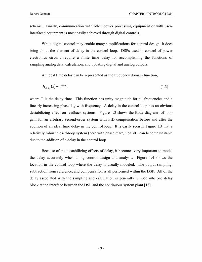
destabilizing effect on feedback systems. Figure 1.3 shows the Bode diagrams of loop
gain for an arbitrary second-order system with PID compensation before and after the
addition of an ideal time delay in the control loop. It is easily seen in Figure 1.3 that a
relatively robust closed-loop system (here with phase margin of 30º) can become unstable
due to the addition of a delay in the control loop.
Because of the destabilizing effects of delay, it becomes very important to model
the delay accurately when doing control design and analysis. Figure 1.4 shows the
location in the control loop where the delay is usually modeled. The output sampling,
subtraction from reference, and compensation is all performed within the DSP. All of the
delay associated with the sampling and calculation is generally lumped into one delay
block at the interface between the DSP and the continuous system plant [13].

Robert Gannett CHAPTER 1 INTRODUCTION
- 10 -
Figure 1.3 Loop gain Bode diagrams before (-) and after (--) addition of control
loop time delay
Figure 1.4 Basic system model including ideal time delay
While the delay associated with digital control may not be a constant for various
reasons, it is important to put bounds on the length of the delay, so that the control can be
designed around these limits. While there may be several different strategies for digital
control implementation, the simplest would be to sample output variables, calculate duty
Robert Gannett CHAPTER 1 INTRODUCTION
- 11 -
cycles, and update the Pulse Width Modulation (PWM) registers all in one switching
cycle. This strategy leads to a delay of between one and two switching periods [14].
Figure 1.5 shows time-domain waveforms depicting how this time delay occurs in a
leading edge PWM scheme.
At the beginning of the first switching period, the output variables are sampled
and held for digital to analog (D/A) conversion. During the first switching period, the
compensation calculations are performed and the PWM registers are updated with new
duty cycles. This duty cycle is then held in the PWM register until the next update at the
end of the second switching period. So the duty cycle implemented at time t2 in Figure
1.5, is the result of the output variables as measured at time t0. The delay time will
consequently be equal to one switching period (sample and calculation time) and the
length of the duty cycle in the second switching period (duty cycle hold time). The delay
time will vary with the duty cycle, and the maximum delay time will be determined by
maximum duty cycle (modulation index). In an analog implementation (delay-free
system) the error signal, and also the compensated duty cycle control output, would not
experience this delay, because they would be continuously changing. For the purposes of
this thesis, the modeled digital delay will be equal to two switching periods as a worst-
case scenario.
To demonstrate the difficulties imposed on control by the digital delay in the
control loop, a brief example will be explored. If an inverter is operating at a switching
frequency of 10 kHz and operating with the calculation and PWM scheme described
above, then the phase lag due to the delay will be 45º at 625 Hz and 90º at 1250 Hz. This
is the frequency range one might expect to find the output filter resonant frequency (for a
60 Hz fundamental). With such a significant phase lag at these frequencies, it would be
very difficult (if not impossible) for a compensator to be designed with a bandwidth
greater than the output filter resonant frequency. Thus, the control loop delay may
necessitate a low control bandwidth and may cause stability issues under light loading, as
described in the section below.

Robert Gannett CHAPTER 1 INTRODUCTION
- 12 -
Figure 1.5 Origins of digital delay time length
1.3.3 No-load Stability Concerns
Under light load or unloaded conditions, the output filter of a VSI is lightly
damped (high Q factor) and will have significant peaking in the frequency domain. This
peaking will appear in the loop gain in the d- and q-channels at the resonant frequency
and in the o-channel at half of the resonant frequency (the reasoning for this will be
discussed in section 1.5). In traditional compensator design for power electronics
circuits, such as for the buck converter, the control bandwidth is generally greater than
the resonant frequency of the output filter. Thus, peaking at the resonant frequency is of
no concern. However, because of the difficulties described in sections 1.3.1 and 1.3.2, it
is generally not possible to achieve a control bandwidth greater than the resonant
frequency of the output filter in a high power inverter. When this is the case, the peaking
of the output filter at light load or no load can cause the loop gain to come back above 0
dB after the intended control bandwidth. If the phase has already rolled off to below –
180º, then the system will be unstable. Figure 1.6 depicts an arbitrary second-order
system with integral compensation under full and light loading conditions. Under full

Robert Gannett CHAPTER 1 INTRODUCTION
- 13 -
load, the system appears to have very conservative stability margins (gain margin of 15
dB and phase margin of 90º); however, under light loading conditions, the system would
obviously be unstable.
Figure 1.6 Loop gain Bode diagrams at full load (-) and light load (--)
Because the peaking of the output filter can cause the converter to become
unstable, measures must be taken to ensure appropriate stability margins under light load
or unloaded conditions. This places additional burdens on the control design.
Techniques for addressing this stability issue are discussed in Chapter 2.
1.3.4 Unbalanced and Distorting Loads
Under unbalanced phase loading, negative sequence and zero sequence distortion
occurs (see Appendix B for an explanation of symmetrical decomposition). This creates
unbalanced phase voltages and unequal phase shifting between phases. Section 1.2
described the concerns associated with applying unbalanced phase voltages to specific
loads. Thus, control strategies must be employed to ensure that phase regulation is

Robert Gannett CHAPTER 1 INTRODUCTION
- 14 -
achieved within certain limits. Chapter 3 will discuss methods to accomplish successful
unbalanced load control.
Non-linear loads, such as diode rectifiers, cause non-linear currents to flow in the
phase conductors. A non-linear current is described as any current that does not have a
linear relationship with the voltage applied to the load. These currents contain, and in
some cases are dominated by, harmonics of the fundamental frequency. If a VSI was an
ideal voltage source, then providing harmonic currents would not be a concern.
However, VSIs have a finite output impedance, and the harmonic currents flowing
through this impedance will create harmonic distortion at the output of the VSI. Section
1.2 described the harmful effects of harmonic distortion in power systems. Several active
and passive techniques for attenuating harmonic distortion have been proposed and
demonstrated in the past. Chapter 4 will detail some old as well as some new techniques
to reduce the THD of the inverter output under non-linear loading.
1.4 400 Hz Systems
Most high power inverter applications are either for 50/60 Hz applications
(traditional utility frequencies) or large motor drives. While variable frequency motor
drives may require fundamental frequencies in excess of 60 Hz, motors are quite
predictable loads. Thus, inverter control strategy for this application is very different
from an inverter in a power distribution role. However, there are a small number of
applications outside of motor drives for high power inverters with higher fundamental
output frequencies.
1.4.1 Applications
400 Hz systems find use in applications where space and weight are at a premium.
Because of a higher fundamental frequency than traditional line frequencies, passive
components in a 400 Hz system can be much smaller. For example, transformers will be
smaller in a 400 Hz system, because the volt-second product (change in flux) will be
smaller due to the shorter period than that for a 60 Hz system. Smaller passive
components enable the power systems to be lighter and take up less volume. In addition,

Robert Gannett CHAPTER 1 INTRODUCTION
- 15 -
a 400 Hz system will enable higher induction motor speeds than are possible in 60 Hz
systems. This is evidenced in equation (1.4), which gives the synchronous speed of an
induction motor,
( )P
frpmSpeed ⋅= 120 , (1.4)
where f is the fundamental line frequency and P is the number of stator poles. It is
easily seen that the synchronous speed of the induction motor is directly proportional to
the line frequency.
For the reasons listed above, 400 Hz systems have long been the standard for
aircraft power distribution systems [15]. 400 Hz systems have also found application in
power systems for large people movers, such as subway trains and other electric trains.
1.4.2 Implications for Control Design
While 400 Hz systems may be beneficial from the power system standpoint, it
makes the already difficult task of inverter control even more challenging. In a 400 Hz
system, the ratio between the fundamental output frequency and the switching frequency
is significantly decreased. This makes the goal of achieving high power quality a more
difficult task.
Because of the higher fundamental output frequency, it would generally be
desirable to increase the resonant frequency of the output filter in order to reduce the size
of the passive components. However, increasing the output filter resonant frequency
makes the task of achieving a control bandwidth greater than the resonant frequency even
more difficult to achieve with sufficient stability margins due to control loop delay.
Finally, the higher fundamental frequency implies that the harmonic frequencies
will also be higher. This fact makes traditional compensation for these harmonics
virtually impossible, because significant loop gain would be required at these
frequencies. Ensuring harmonic distortion within acceptable limits will thus require
alternative passive or active means.

Robert Gannett CHAPTER 1 INTRODUCTION
- 16 -
As is seen in the paragraphs above, the difficulties with high power inverters are
only magnified when the output fundamental frequency is increased to 400 Hz.
Therefore, techniques must be developed to guarantee stability and acceptable
performance of the inverter.
1.5 Voltage Source Inverter Under Study
In order to demonstrate the control techniques described in this thesis, it is useful
to show simulation results based on a specific example. For this purpose, a single
inverter model is developed and used throughout this document. The switching and
average models described below are based on a three-phase, four-leg inverter rated at 90
kVA with a 115 Vrms, 400 Hz output.
1.5.1 Inverter Switching Model
The switching model of the inverter is developed in order to be as close to a truth
model as possible. This model should give accurate time domain waveforms for the
inverter under various loading conditions and transients. Figure 1.7 shows a schematic of
the inverter switching model, and Table 1.5 gives the parameters for the inverter model.
The fourth leg enables control of the neutral current. In three-phase, three-leg
inverters, if the load requires a neutral connection, this point is usually connected to the
neutral point of the filter capacitors or to the midpoint of the DC link. When this is the
case, unbalanced loads or single phase non-linear loads will cause neutral currents to flow
and zero sequence distortion. When a fourth leg is employed, the neutral point is
controlled, and zero sequence distortion can be reduced through control strategies.

Robert Gannett CHAPTER 1 INTRODUCTION
- 17 -
Figure 1.7 Schematic of the switching model of a four-leg inverter
Table 1.5 Inverter Switching Model Parameters
ValueVin 600 - 700 VDC
Vout,l-n 115 Vrms, 400 HzPout,total 90 kVALfilter 42.8 µHLn 42.8 µHCfilter 250 µFfs 15.6 kHztrise 200 nstfall 150 nsRon 1 mΩ
Parameter
Input/Output
Filter Components
Switch Characteristics
1.5.2 Inverter Average Model
While the switching model is a good model of the physical inverter, it is non-
linear because of the switches. For this reason, a representative linear model must be
developed so that the frequency domain characteristics of the system can be studied.
Also, simulation times for an average model are greatly reduced over those for a
switching model, because the simulation time step can be increased (switching frequency
components are not present in the average model). These two reasons make the average
model ideal for control design and development.
Robert Gannett CHAPTER 1 INTRODUCTION
- 18 -
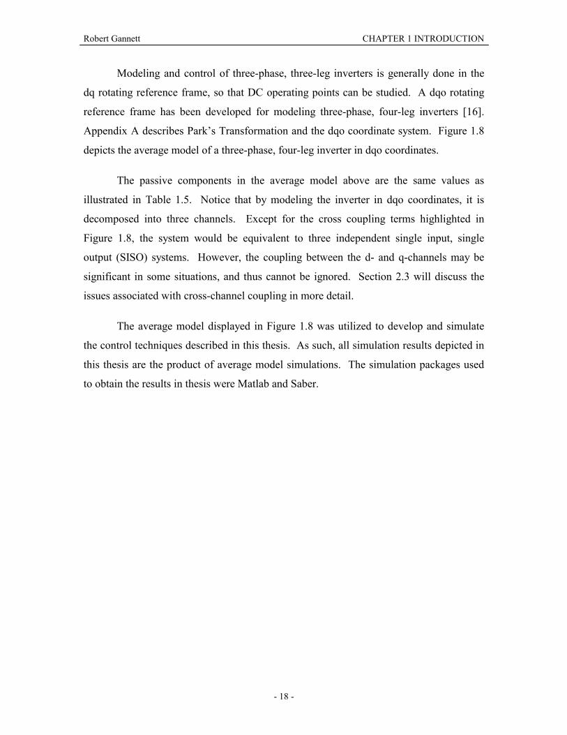
Modeling and control of three-phase, three-leg inverters is generally done in the
dq rotating reference frame, so that DC operating points can be studied. A dqo rotating
reference frame has been developed for modeling three-phase, four-leg inverters [16].
Appendix A describes Park’s Transformation and the dqo coordinate system. Figure 1.8
depicts the average model of a three-phase, four-leg inverter in dqo coordinates.
The passive components in the average model above are the same values as
illustrated in Table 1.5. Notice that by modeling the inverter in dqo coordinates, it is
decomposed into three channels. Except for the cross coupling terms highlighted in
Figure 1.8, the system would be equivalent to three independent single input, single
output (SISO) systems. However, the coupling between the d- and q-channels may be
significant in some situations, and thus cannot be ignored. Section 2.3 will discuss the
issues associated with cross-channel coupling in more detail.
The average model displayed in Figure 1.8 was utilized to develop and simulate
the control techniques described in this thesis. As such, all simulation results depicted in
this thesis are the product of average model simulations. The simulation packages used
to obtain the results in thesis were Matlab and Saber.

Robert Gannett CHAPTER 1 INTRODUCTION
- 19 -
Figure 1.8 Four-leg inverter average model in dqo coordinates
1.6 Objectives
In light of the numerous applications for high power, high performance inverters
in the modern world, and the difficulties involved in their design, it is the objective of this
thesis to explore several advanced control topics for increased inverter performance
under challenging loading conditions. Presently, there is a significant lack of applied
inverter control techniques to meet the high level of power quality demanded by today’s
advanced technology. In order to produce acceptable power waveforms from high power
inverters, extra hardware is usually employed. However, additional power circuitry is
bulky, expensive, and lossy. Therefore, it is the goal of this thesis to present some
advanced inverter control strategies to achieve superior performance without the
disadvantages of excessive hardware.

Robert Gannett CHAPTER 1 INTRODUCTION
- 20 -
Chapter 2 will discuss stability concerns at light load in more detail and will
present control techniques to ensure stable operation at light load. Modeling of three-
phase inverters and the issue of cross-channel coupling in dqo coordinates will also be
reviewed and reexamined in Chapter 2. Traditional and new advanced control strategies
to compensate for unbalanced loading will be introduced and compared in chapter 3. A
research topic of particular interest over the last several years has been harmonic control
in inverters to compensate for the distorting effect of non-linear loading. Chapter 4 will
present the concept of harmonic control, its extension to four-leg inverters, and a
comparison to traditional harmonic reduction techniques. Finally, chapter 5 will close
with some concluding thoughts and topics for future research.
Robert Gannett CHAPTER 2 NO-LOAD CONDITIONS
- 21 -
2 NO-LOAD CONDITIONS
All inverters, regardless of their application, may face light load or no-load
conditions. This situation can occur in one of two manners. First, the power required
from the load of the inverter may drop near or to zero. Second, under an output fault
condition, such as an open breaker or fuse, the inverter will experience unloaded
conditions. This second situation can occur for any inverter in any application, because
safety standards require protective circuitry between power sources and loads.
Regardless of the cause of the light or unloaded conditions, proper operation of the
inverter must be maintained.
2.1 Stability Issues
As was introduced in Section 1.3.3, the issue of stability can arise under light
loading. This section will introduce the origins of the stability problem.
2.1.1 Open Loop Plant Transfer Functions
The open loop transfer functions developed below will facilitate the discussions
on stability in this chapter.
2.1.1.1 Open Loop Control to Output Transfer Function
First, taking the cross-channel coupling terms to be insignificant, each of the
channels in the average model of the inverter degenerate into simple SISO buck converter
average models. The state equations for each channel would then be,
[ ]
⋅=
⋅
+
⋅
⋅−
−=
C
Loqd
oqd
DC
C
L
load
C
L
VI
V
DLV
VI
CRC
LVI
10
011
10
,,
,,
, (2.1)

Robert Gannett CHAPTER 2 NO-LOAD CONDITIONS
- 22 -
where oqdD ,, is the individual dqo channel’s duty cycle, loadR is the balanced phase load
resistance, and C and L are the channel’s passive components as displayed in Figure 1.8.
From the state equations, the plant control to output transfer function is
( )( ) 21 sCLs
RL
VsH
load
DCv
⋅+⋅
+
= . (2.2)
Equation (2.2) can be placed in the traditional second-order low pass filter form,
( ) 20
1
+
⋅+
=
oo
vv
sQ
s
HsH
ωω
, (2.3)
with the following definitions,
DCv VH =0 , (2.4)
CLo ⋅= 1ω , (2.5)
LCRQ load ⋅= . (2.6)
It is easy to see from these definitions that under no-load conditions ( )∞=loadR ,
the output filter is undamped and the Q factor will be infinite. While this may be the case
for an ideal output filter, this is not representative of the actual physical system. By
adding parasitic resistances into the output filter model, as seen in Figure 2.1, the output
filter will be lightly damped by its own parasitics at no-load. LR and CR were chosen to
be Ωm10 for this study. Because of the dqo coordinate transformation, LR in the o-
channel will be two times the filter inductor ESR.

Robert Gannett CHAPTER 2 NO-LOAD CONDITIONS
- 23 -
Figure 2.1 DQO channel average model including parasitic resistances
From the average model above, the following state space equations are developed,
( ) ( )
( ) ( )
⋅
++⋅
=
⋅
+
⋅
+⋅−
+⋅−
+⋅−
+⋅⋅
−−=
C
L
Cload
load
Cload
Cloadoqd
oqd
DC
C
L
CloadCload
C
Cload
load
Cload
CloadL
C
L
VI
RRR
RRRRV
DLV
VI
RRCRRCR
C
RRLR
RRLRR
LR
VI
,,
,,011
. (2.7)
From this set of state space equations, the following plant control to output transfer
function can be derived,
( ) 2
0
1
1
+
⋅+
+⋅
=
oo
zv
vs
Qs
sHsH
ωω
ω, (2.8)
with the following definitions,
+⋅=
Lload
loadDCv RR
RVH 0 , (2.9)

Robert Gannett CHAPTER 2 NO-LOAD CONDITIONS
- 24 -
Cz RC ⋅
= 1ω , (2.10)
Cload
Lloado RCLRCL
RR⋅⋅+⋅⋅
+=ω , (2.11)
( ) ( )( )CLCloadLload
LloadCload
RRRRRRCLRRRCLRCL
Q⋅+⋅+⋅⋅+
+⋅⋅⋅+⋅⋅= . (2.12)
The definitions above reveal two things about the control to output transfer
function when parasitic resistances are included. First, the addition of the capacitor ESR
results in a high frequency zero in equation (2.8). Second, the combination of the
capacitor and inductor ESRs adds damping to the filter, even at no-load. Figure 2.2
displays the dqo channel control to output transfer functions for the VSI under study at
light load.
Figure 2.2 Bode plots of the plant control to output transfer functions for the d- and
q-channels (-) and the o-channel (--)

Robert Gannett CHAPTER 2 NO-LOAD CONDITIONS
- 25 -
The resonant frequency for the o-channel is half of that for the d- and q-channels.
This is because the equivalent inductance for the o-channel is four times of that for the d-
and q-channels. Thus, separate control designs will be required for the d- and q-channels
and the o-channel.
2.1.1.2 Open Loop Control to Inductor Current Transfer Function
Using the state space equations in (2.7), including filter parasitic resistances, the
following plant control to inductor current transfer function can be developed,
( ) 2
0
1
1
+
⋅+
+⋅
=
oo
zi
is
Qs
sHsH
ωω
ω, (2.13)
with the following definitions,
+=
LloadDCi RR
VH 10 , (2.14)
Cloadz RCRC ⋅+⋅
= 1ω , (2.15)
Cload
Lloado RCLRCL
RR⋅⋅+⋅⋅
+=ω , (2.16)
( ) ( )( )CLCloadLload
LloadCload
RRRRRRCLRRRCLRCL
Q⋅+⋅+⋅⋅+
+⋅⋅⋅+⋅⋅= . (2.17)
These definitions reveal that the Q factor and the resonant frequency for the plant
control to inductor current transfer function is the same as for the plant control to output
transfer function. However, the plant control to inductor current transfer function has a
DC gain and a zero that vary greatly as the load resistance varies. The dqo channel

Robert Gannett CHAPTER 2 NO-LOAD CONDITIONS
- 26 -
control to inductor current transfer functions for the VSI under study are shown in Figure
2.3.
Figure 2.3 Bode plots of the control to inductor current transfer functions for the d-
and q-channels (-) and the o-channel (--)
2.1.1.3 Transfer Functions with Cross-Channel Coupling
The plant transfer functions above were developed assuming that the cross-channel
coupling terms were insignificant. This allows each of the dqo channels to be reduced to
a second-order SISO system. However, the cross-coupling terms are often not
insignificant, and must be considered. By adding the cross-coupling terms, the d- and q-
channels merge to become a fourth-order two-input, two-output system. Essentially, this
will result in the plant transfer functions, described in (2.8) and (2.13), having an
additional pair of poles and an additional pair of zeros. Figures 2.4 and 2.5 show the
result of adding the cross coupling terms to the d- and q-channel control to the open loop
transfer functions. The o-channel transfer functions are unaffected, because the o-

Robert Gannett CHAPTER 2 NO-LOAD CONDITIONS
- 27 -
channel is completely decoupled from the d- and q-channels. Cross-channel coupling
issues will be discussed in more detail in Section 2.3.
Figure 2.4 Bode plots of the control to output transfer functions with coupling
terms for the d- and q-channels (-) and o-channel (--)
Figure 2.5 Bode plots of the control to inductor current transfer functions with
coupling terms for the d- and q-channels (-) and o-channel (--)

Robert Gannett CHAPTER 2 NO-LOAD CONDITIONS
- 28 -
2.1.2 Analysis of Plant Transfer Functions
If traditional voltage loop control is to be employed, then the plant characteristics,
as depicted in Figure 2.4, must be compensated for. However, the output filter is very
lightly damped at no-load, and so the plant poles have a very large imaginary component.
Thus, the phase roll-off due to the filter poles is very steep, with the phase dropping close
to –180º near to the resonant frequency. This characteristic would make it very difficult
to extend the control bandwidth beyond the resonant frequency with traditional PID
compensation, especially when the delay due to digital implementation is considered.
It would be possible to directly cancel the poles at no-load by using a set of
imaginary zeros in the compensator. However, under full inverter load, the filter poles
are almost completely real and will not be directly canceled by the imaginary zeros in the
compensator. Thus, some type of adaptive control would be needed in order to cancel the
filter poles under all loading conditions. However, the topic of adaptive control is
beyond the scope of this thesis and would be unnecessary if other techniques could
achieve similar results.
2.2 No-Load Control Design
This section will present the traditional approach to ensure stable operation under
unloaded inverter output, and its shortcomings. A technique to ensure stable inverter
operation at light load or no-load while extending the control bandwidth over
conventional voltage-loop control will also be discussed.
2.2.1 Conventional Voltage Loop Control
In traditional VSI control, voltage compensation is performed in the dqo reference
frame rotating at the fundamental frequency to ensure good regulation of the fundamental
component of the output. Often integral, PI, or PID compensation is employed to achieve
zero steady state error at the fundamental frequency. Because of the difficulties
associated with high power inverter control design, as described in Section 1.3, it is
generally not possible to attain a voltage loop control bandwidth greater than the resonant

Robert Gannett CHAPTER 2 NO-LOAD CONDITIONS
- 29 -
frequency under light loading conditions. Thus, conventional thinking requires the
bandwidth of the voltage loop to be sufficiently low such that the peaking of the filter
will not cross above 0 dB under light load or no-load.
2.2.1.1 Conventional Voltage Loop Design Example
In order to design a voltage loop that will be stable at no-load, the Q factor of the
output filter at no-load must be determined. Equation (2.17) gives a good estimate of the
Q factor when the ESRs of the inductor and capacitor are measured or estimated well.
The true peaking of the physical output filter may be slightly different than the estimated
value due to additional unmodeled parasitics. This is the justification for designing
sufficient gain margin into the system.
At no-load, ∞→loadR , and equation (2.17) can be simplified to,
CL
RRQ
CL
⋅+
= 1 . (2.18)
Given equation (2.18), the Q factors for each of the dqo channels of the inverter under
study at no-load can be calculated. The Q factor for the d- and q-channels is estimated to
be 20.69 or 26.3 dB. It is calculated to be 27.58 or 28.8 dB for the o-channel.
If integral control is used in the voltage compensation, then the loop gain will roll
off at 20 dB per decade before the resonant frequency. The loop gain is defined here as
the compensator times the control to output transfer function times the gain of the return
path, and is used to determine the closed-loop stability of the controlled system.
Designing a conservative gain margin of 12 dB, combined with the 26 to 28 dB of
peaking at the resonant frequency, will require the loop gain crossover frequency to be 2
decades below the resonant frequency. For the case of the inverter under study, the
resonant frequency in the d- and q- channels is 1.54 kHz, and thus the loop gain crossover
frequency must be around 15 Hz. The o-channel resonant frequency is half of the d- and
q- channels, and subsequently the loop gain crossover frequency for the o-channel must
also be half. Using the designed loop gain crossover frequencies above, Figure 2.6

Robert Gannett CHAPTER 2 NO-LOAD CONDITIONS
- 30 -
displays the loop gains at no-load, and Figure 2.7 shows the resulting closed loop system
model for each channel. Table 2.1 depicts the compensator gains as implemented for
each channel.
Figure 2.6 Bode plots of the loop gain containing integral voltage loop
compensation for the d- and q-channels (-) and the o-channel (--)
Figure 2.7 Closed loop inverter model containing integral compensation for each
channel

Robert Gannett CHAPTER 2 NO-LOAD CONDITIONS
- 31 -
Table 2.1 Integral Compensator Design Parameters
Parameter ValueKid 0.16Kiq 0.16Kio 0.08
2.2.1.2 Conventional Approach Analysis
The conventional voltage loop control design successfully achieves a robust
design, with conservative gain margins of approximately 12 dB and phase margins of
approximately 90º at no-load. This control will achieve zero steady state error for the
fundamental output waveforms, because the compensator integrates the error signal.
However, this design also results in the extremely low control bandwidths of 15 Hz and 7
Hz for the dq-channels and the o-channel, respectively. This low control bandwidth will
result in slow transient responses to load changes and poor performance under
unbalanced and distorting loads.
While this conventional control strategy may provide acceptable performance for
certain applications, it certainly produces poor results under the types of loading
conditions typical for many high power inverter applications. For most applications, it
would be beneficial to realize higher control bandwidths.
2.2.2 Inner Current Loop Control
Inner current control loops are often used in DC/DC converters in order to
achieve several improvements in control performance [17]. By designing an inner
current loop, voltage loop design is simplified and better transient response to load
change can be accomplished [18]. Because three-phase VSIs are often modeled as buck
converters in the dqo coordinate system, similar control performance improvements
should be possible in three- and four-leg inverters.
2.2.2.1 Inner Control Loop Concept
Figure 2.8 depicts a closed loop system with an inner (minor) and outer (major)
loop. The minor loop can be viewed as a forward path transfer function with its own

Robert Gannett CHAPTER 2 NO-LOAD CONDITIONS
- 32 -
independent poles that can be adjusted separately through the minor loop gain [19]. This
may enable performance gains for the entire closed loop system.
Figure 2.8 Nested Control Loops
From Figure 2.8, the closed loop transfer functions and loop gains of the two
loops can be developed. The minor loop gain is given by,
( ) ( ) ( )sHGsHsG 11=⋅ , (2.19)
and the closed minor loop reference to output transfer function is,
( ) ( )( )sHG
sHGsT11
111 1+
= . (2.20)
The closed minor loop reference to output transfer function now becomes a forward path
transfer function in the major loop. Thus, the major loop gain is
( ) ( ) ( )( )sHG
sHHGGsHsG11
2112
1+=⋅ , (2.21)
and the closed major loop reference to output transfer function becomes,
( ) ( )( )
( )( ) ( )sHHGGsHG
sHHGGsRsYsT
211211
21122 1 ++
== . (2.22)

Robert Gannett CHAPTER 2 NO-LOAD CONDITIONS
- 33 -
The equations developed above will enable an inner current loop control strategy
to be designed, and its benefits explored.
2.2.2.2 Inner Control Loop Applied to Inverters
In order to make use of an inner control loop, the inverter model must be
reconfigured to be of the form shown in Figure 2.8. Figure 2.9 depicts the new system
model for each channel, with ( )sH i representing the plant control to inductor current
transfer function, and ( )sH v representing the plant control to output transfer function.
Figure 2.9 System model including inner and outer control loops
Using this model and equation (2.20), the closed inner current loop reference to
output transfer function becomes,
( ) ( )( )sHG
sHGsTikik
ikik
+=
11 , (2.23)
and the outer voltage loop gain that results is,
( ) ( ) ( )( )sHGsHGGsHsG
ikik
vkikvk
+=⋅
1. (2.24)

Robert Gannett CHAPTER 2 NO-LOAD CONDITIONS
- 34 -
If ( )sGvk is initially taken to be unity, it is clear to see from equation (2.24) that
the poles of the voltage loop gain will be the zeros of ( )sHG ikik+1 . This results because
the poles of ( )sHik are exactly the same as the poles of ( )sH vk (see equations (2.8) and
(2.13) for validation of this comment). Thus, through the choice of ( )sGik , the zeros of
( )sHG ikik+1 can be designed such that the peaking in the voltage loop gain will be
eliminated. This possibility is best demonstrated through an expansion of ( )sHG ikik+1 .
Assuming ( )sGik to be the simple proportional gain iG ,
( )( )
2
2
00
1
111
+
⋅+
+⋅
⋅+
⋅+⋅+
=+
oo
oz
ii
oii
ikiks
Qs
ssHGQ
HGsHG
ωω
ωωω. (2.25)
Using equation (2.25), bounds can be placed on iG , such that the zeros of
( )sHG ikik+1 will not introduce peaking. First, under light load or no-load, the 0ii HG ⋅
term will be insignificant compared to 1 and can be ignored in the 0s term in the
numerator, because loadR is very large (see equation (2.14) for justification). Thus, the
numerator of (2.25) is of the standard second-order form. In this form, the Q factor of the
second order equation must be less than or equal to 2
1 in order to prevent peaking.
This constraint is defined as,
oz
ii
o
HGQ ωωω
21 0 ≥
⋅+
⋅. (2.26)
Using the definitions identified in Section 2.1.1.2, this inequality can be redefined as,
( ) ( ) ( )( )LloadDC
CLCloadLloadLloadCloadi RRVC
RRRRRRCLRRRCLRCLG
+⋅⋅⋅+⋅+⋅⋅−−+⋅⋅⋅+⋅⋅⋅
≥2
. (2.27)

Robert Gannett CHAPTER 2 NO-LOAD CONDITIONS
- 35 -
At no-load, ∞→loadR , and inequality (2.27) reduces to,
DC
CL
i V
RRCL
G−−⋅
≥2
. (2.28)
Inequality (2.28) sets a lower bound for the value of iG in order to prevent
peaking in the voltage loop gain. If a value of iG greater than the critical value shown in
(2.28) is chosen, then the Q factor (left side of (2.26)) of the pair of zeros in ( )sHG ikik+1
will decrease. At a Q factor of 0.5 the zeros become purely real, and if iG is increased
further, then the zeros remain purely real and split along the real axis. There will also be
a maximum bound on the value of iG determined by the phase margin requirements of
the inner loop. Even if sufficient phase margin is not achievable with the critical value
shown in (2.28), then a value for iG smaller than this will still reduce the imaginary
component of the plant poles in the voltage loop gain, which will consequently reduce the
peaking. Now that the peaking in the voltage loop gain can be reduced or eliminated, the
voltage compensation transfer function, ( )sGvk , can be chosen such that significant gains
in the voltage loop control bandwidth are achieved while maintaining sufficient stability
margins.
2.2.2.3 Inner Current Loop Control Design
Making use of the previous section, an inner current loop can be designed for the
inverter under study in order to extend the voltage control loop bandwidth under
unloaded conditions. Using equation (2.28), for no-load conditions, the minimum value
of iG for the d- and q-channels is 0.00092, and is 0.00186 for the o-channel.
Using these minimum values for iG , Figure 2.10 displays the inner current loop
gains for the channels and Figure 2.11 shows the resulting closed inner current loop
reference to output transfer function. This resulting transfer function can now be thougt
of as the voltage loop plant. The derivations above, in Section 2.2.2.2, neglect the cross
coupling terms in the d- and q-channels; however, the technique still results in significant

Robert Gannett CHAPTER 2 NO-LOAD CONDITIONS
- 36 -
reduction of the peaking in the voltage loop, as shown in Figure 2.11. Comparing these
results to the plant control to output transfer functions in Figure 2.4, the benefits of the
inner current loop are easily grasped.
Figure 2.10 Inner current loop gain Bode diagrams for the d- and q-channels (-)
and the o-channel (--)
Figure 2.11 Bode diagrams of the closed inner current loop reference to output
transfer function for the d- and q-channels (-) and the o-channel (--),

Robert Gannett CHAPTER 2 NO-LOAD CONDITIONS
- 37 -
The previous plots were shown in order to prove the inner current loop concept,
but the modeled delay was ignored for these results. When the modeled delay is set to
the realistic value of two switching periods, then the ensuing phase roll off causes the
inner closed loop to become unstable. Consequently, some phase lead is required near
the crossover frequencies in order to ensure proper stability margins. Traditionally, this
would be accomplished by placing a zero(s) near the crossover frequency. This may
achieve the desired results, but a more efficacious strategy is to use complex zeros.
Complex zeros result in downward peaking (notching) and sharp phase lead at the
resonant frequency in the frequency domain. In order to demonstrate these
characteristics, figure 2.12 shows the transfer function for an arbitrarily chosen set of
complex zeros at 1000 rad/sec, with a Q factor of 2, and a set of real poles at 2000
rad/sec. The poles are required in order to make the transfer function proper (the number
of poles greater than or equal to the number zeros). The characteristics described above
can be utilized to either increase the phase margin at the crossover frequency, or to
increase the gain margin after the crossover frequency, or a combination of both. It is up
to the control designer to choose the location of the poles and zeros in order to achieve
the appropriate stability margins.
Figure 2.12 Transfer function utilizing complex zeros

Robert Gannett CHAPTER 2 NO-LOAD CONDITIONS
- 38 -
Utilizing the characteristics of complex zeros, the inner current loop can be
stabilized, and its benefits still reaped. Figure 2.13 displays the new inner current loop
gains, including the modeled digital delay and making use of complex zeros. The chosen
current loop compensator transfer functions are displayed in Table 2.2. Comparing these
results to the case without the modeled delay (Figure 2.10), it is clear to see that some
gain is lost in order to stabilize the loop. As a result, the peaking of the voltage loop
poles will not be completely eliminated, but will still be significantly reduced.
Figure 2.13 Inner current loop gain Bode diagrams for the d- and q-channels (-)
and the o-channel (--) with modeled delay and complex zero compensation
Closing this inner current loop significantly decreases the voltage loop peaking,
even under unloaded conditions. With this benefit, a simple integral controller can be
designed to achieve higher bandwidths than were possible without closing the inner
current loop. Figure 2.14 shows the closed loop system for each channel, and Table 2.2
gives the compensator parameters as simulated for the inverter under study. Figure 2.15
displays the resulting outer voltage loop gains (integral compensator times closed inner
current loop reference to output transfer function times unity return path gain). The

Robert Gannett CHAPTER 2 NO-LOAD CONDITIONS
- 39 -
current loop compensator gains have been increased slightly in order to compensate for
the decreased gain due to the complex zeros.
Figure 2.14 Closed loop inverter model with inner and outer control loops
Table 2.2 Inner and Outer Loop Compensator Design Parameters
Parameter Value
( )sGvd s6000
( )sGvqs
6000
( )sGvo s1000
( )( )2
2
20000816.180000015.0
++⋅+⋅
sess
( )( )2
2
20000816.180000015.0
++⋅+⋅
sess
( )( )2
2
20000845.116000003.0
++⋅+⋅
sess
( )sGid
( )sGiq
( )sGio
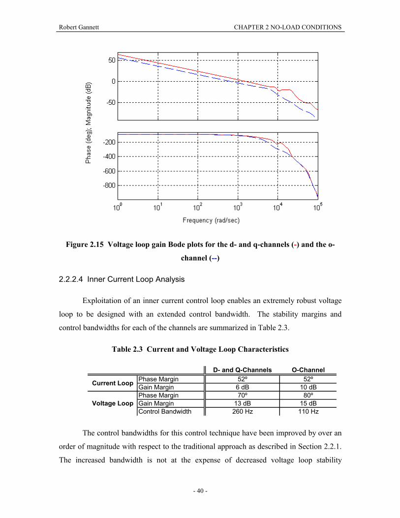
Robert Gannett CHAPTER 2 NO-LOAD CONDITIONS
- 40 -
Figure 2.15 Voltage loop gain Bode plots for the d- and q-channels (-) and the o-
channel (--)
2.2.2.4 Inner Current Loop Analysis
Exploitation of an inner current control loop enables an extremely robust voltage
loop to be designed with an extended control bandwidth. The stability margins and
control bandwidths for each of the channels are summarized in Table 2.3.
Table 2.3 Current and Voltage Loop Characteristics
D- and Q-Channels O-ChannelPhase Margin 52º 52ºGain Margin 6 dB 10 dBPhase Margin 70º 80ºGain Margin 13 dB 15 dBControl Bandwidth 260 Hz 110 Hz
Current Loop
Voltage Loop
The control bandwidths for this control technique have been improved by over an
order of magnitude with respect to the traditional approach as described in Section 2.2.1.
The increased bandwidth is not at the expense of decreased voltage loop stability

Robert Gannett CHAPTER 2 NO-LOAD CONDITIONS
- 41 -
margins. These gains have been achieved while maintaining simple integral voltage loop
control. Further gains in control bandwidth may be achievable with the implementation
of PID controllers, increasing the transient performance of the VSI.
It is important to note that all practical compensators must roll-off at high
frequencies, and that this low pass filtering must occur below the switching frequency in
all switching converter feedback control systems. In addition, digital systems require
anti-aliasing filters to ensure proper performance of the control system. Anti-aliasing can
be accomplished through a first-order low pass filter with a cutoff frequency below the
digital sampling frequency. Often a single compensator pole near the converter
switching frequency is utilized to perform both functions. Regardless, the frequency of
this compensator pole with respect to the control crossover frequency will lead to
additional phase lag at the crossover frequency, and likewise, a reduction in the phase
margin.
It is interesting to note that the stability margins are not as great, and the peaking
is more pronounced, in the d- and q-channels as compared to the o-channel. This is due
to the increased phase roll-off from the modeled delay at the frequencies of interest for
the d- and q-channels.
Assuming current sensors would already be in place for overcurrent monitoring,
adding the inner current loop would require no significant additional hardware for
implementation. The inner loop would, however, involve additional processing time.
But considering the present-day processing speed of DSPs, it would likely be an
insignificant amount of time compared to the switching period.
2.2.3 No-Load Control Summary
The conventional approach to ensuring stability under unloaded conditions is to
simply decrease the voltage loop gain crossover frequency until sufficient stability
margins are achieved. While this approach can accomplish a very robust design, it will
have an extremely low control bandwidth, which will limit transient performance of the
inverter.

Robert Gannett CHAPTER 2 NO-LOAD CONDITIONS
- 42 -
Closing an inner current loop is a traditional technique in DC/DC converters to
improve transient performance, and a similar approach has been presented here to attain
similar benefits for high power inverters. By introducing a current loop, the peaking of
the voltage loop poles can be reduced or eliminated. This enables significant
improvement of the closed loop bandwidth of the system, as evidenced above.
The limiting factor in the voltage loop design using the traditional approach
(Section 2.2.1) is the peaking of the output filter poles. By closing an inner current loop,
this factor can be virtually eliminated, and the limiting factor becomes the phase roll-off
of the control delay. This is an uncontrollable aspect of implementing the control
digitally, and thus it pushes the boundaries of this implementation.
While the multiple loop control strategy provides the possibility of extending the
control bandwidth, it may not be increased enough to significantly attenuate harmonics of
the fundamental output frequency. This becomes especially true for high power, high
fundamental frequency inverters, where the ratio of fundamental frequency to switching
frequency is small. Consequently, the technique of a closed inner loop may improve
dynamic response to load changes, but other techniques must be applied in order to
manage the distortion due to unbalanced and non-linear loads. Chapters 3 and 4 will
present such techniques.
2.3 Cross-Channel Coupling
It would be desirable if the transformation from abc coordinates to dqo
coordinates would result in an average three-phase, four-leg inverter model with three
independent SISO channels. However, the resulting model has some cross-coupling
between the states in the d- and q-channels. This section will explore the benefits and
possibility of decoupling the d- and q-channels.

Robert Gannett CHAPTER 2 NO-LOAD CONDITIONS
- 43 -
2.3.1 Cross-Coupling Transfer Functions
Because the coupling between the d- and q-channels may be significant, the
channels must be viewed as a Multiple Input, Multiple Output (MIMO) system. The state
space equations for this system take the form,
[ ] [ ] [ ][ ] [ ]TCqLqCdLd
Tqd
Tqd
TCqLqCdLd
TCqLqCdLd
VIVICVV
DDBVIVIAVIVI
⋅=
⋅+⋅=
, (2.29)
with the matrix definitions,
( ) ( )
( ) ( )
( ) ( )
( ) ( )
+−
+−−
+−−
+⋅
−−
+−
+−
+−−
+⋅
−
=
CloadCload
C
Cload
loadL
Cload
Cload
CloadCload
C
Cload
loadL
Cload
Cload
RRCRRCR
C
RRLR
LR
RRLRR
RRCRRCR
C
RRLR
LR
RRLRR
A
110
0
011
0
ω
ω
ω
ω
, (2.30)
=
00
000
0
LV
LV
BDC
DC
, (2.31)
++⋅
++⋅
=
Cload
load
Cload
Cload
Cload
load
Cload
Cload
RRR
RRRR
RRR
RRRR
C00
00. (2.32)
In the form above, the dq-channel MIMO system will have the four transfer
functions, ,~~
,~~
,~~
d
q
q
d
d
d
dv
dv
dv and
q
q
dv~~
. The transfer functions q
d
dv~~
and d
q
dv~~
are the cross-
coupling transfer functions, and would be identically zero for all frequencies if the

Robert Gannett CHAPTER 2 NO-LOAD CONDITIONS
- 44 -
channels were completely decoupled. The cross-coupling transfer functions become
most significant under lightly loaded or unloaded conditions. Figure 2.15 compares the
d-channel control to output transfer function to the cross-coupling transfer function q
d
dv~~
at
no-load. Because of the symmetry between the d- and q-channels, the results will be the
same for the q-channel, except that the cross-coupling transfer function will be 180º out
of phase due to the change in signs.
Figure 2.16 Open loop d-channel control to output (-) and cross-coupling (--)
transfer functions
It is clear that the cross-coupling is significant around the resonant frequency at
light load. As a result, the control to output transfer function has two sets of complex
poles and one set of complex zeros near the resonant frequency of the output filter. This
causes the double peaking present in the plot.
2.3.2 Advantages of Decoupling
Usually, three-phase inverter control is approached with independent
compensators for each channel. This implies that the cross-coupling is assumed to be
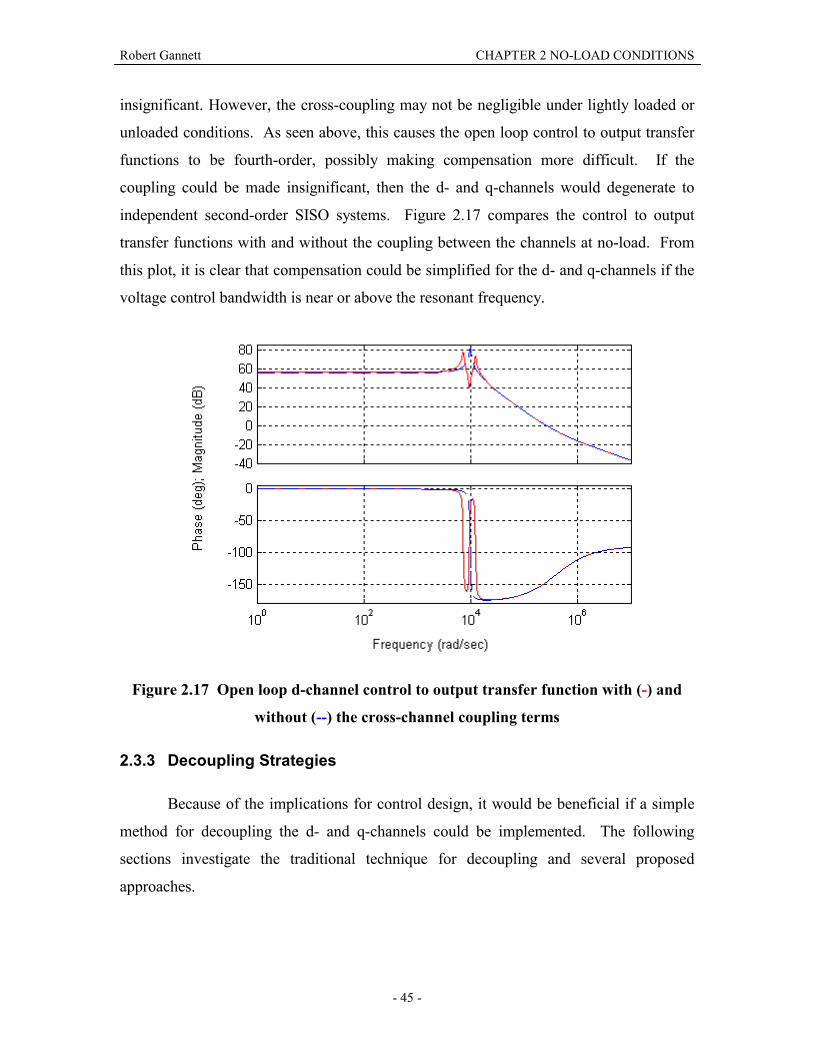
Robert Gannett CHAPTER 2 NO-LOAD CONDITIONS
- 45 -
insignificant. However, the cross-coupling may not be negligible under lightly loaded or
unloaded conditions. As seen above, this causes the open loop control to output transfer
functions to be fourth-order, possibly making compensation more difficult. If the
coupling could be made insignificant, then the d- and q-channels would degenerate to
independent second-order SISO systems. Figure 2.17 compares the control to output
transfer functions with and without the coupling between the channels at no-load. From
this plot, it is clear that compensation could be simplified for the d- and q-channels if the
voltage control bandwidth is near or above the resonant frequency.
Figure 2.17 Open loop d-channel control to output transfer function with (-) and
without (--) the cross-channel coupling terms
2.3.3 Decoupling Strategies
Because of the implications for control design, it would be beneficial if a simple
method for decoupling the d- and q-channels could be implemented. The following
sections investigate the traditional technique for decoupling and several proposed
approaches.

Robert Gannett CHAPTER 2 NO-LOAD CONDITIONS
- 46 -
2.3.3.1 Traditional Approach
The cross-coupling terms can be viewed as uncontrollable inputs into each of the
channels. Taking this approach, the state space equations for the d-channel model can be
written as in equation (2.33). The state space equations for the q-channel model are the
same, except that the sign of the cross-coupling terms is reversed.
( ) ( )
( ) ( )
⋅
++⋅
=
⋅
+⋅
+
⋅
+−
+−
+−−
+⋅
−=
Cd
Ld
Cload
load
Cload
Cloadd
Cq
lqd
DC
Cd
Ld
CloadCload
C
Cload
loadL
Cload
Cload
Cd
Ld
VI
RRR
RRRR
V
VI
DLV
VI
RRCRRCR
C
RRLR
LR
RRLRR
VI
ωω0
0
011
(2.33)
Viewing the state space equations in (2.33), it is evident that feedforward terms
could be added to the control input dD in order to cancel out the LqI cross-coupling term.
This is demonstrated graphically in the model depicted in Figure 2.18.
Figure 2.18 D- and q-channel models including the decoupling terms
A simple calculation yields the decoupling term, DC
Lq
VIL ⋅⋅
−ω
, that can be added
to the control input dD in order to cancel the cross-coupling due to LqI . The q-channel
decoupling term will simply have the sign reversed.
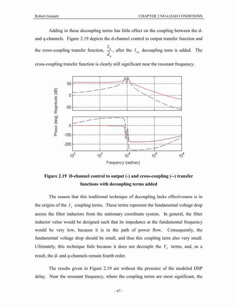
Robert Gannett CHAPTER 2 NO-LOAD CONDITIONS
- 47 -
Adding in these decoupling terms has little effect on the coupling between the d-
and q-channels. Figure 2.19 depicts the d-channel control to output transfer function and
the cross-coupling transfer function, q
d
dv~~
, after the LqI decoupling term is added. The
cross-coupling transfer function is clearly still significant near the resonant frequency.
Figure 2.19 D-channel control to output (-) and cross-coupling (--) transfer
functions with decoupling terms added
The reason that this traditional technique of decoupling lacks effectiveness is in
the origins of the LI coupling terms. These terms represent the fundamental voltage drop
across the filter inductors from the stationary coordinate system. In general, the filter
inductor value would be designed such that its impedance at the fundamental frequency
would be very low, because it is in the path of power flow. Consequently, the
fundamental voltage drop should be small, and thus this coupling term also very small.
Ultimately, this technique fails because it does not decouple the CV terms, and, as a
result, the d- and q-channels remain fourth order.
The results given in Figure 2.19 are without the presence of the modeled DSP
delay. Near the resonant frequency, where the coupling terms are most significant, the

Robert Gannett CHAPTER 2 NO-LOAD CONDITIONS
- 48 -
delay phase roll-off causes the decoupling terms to no longer directly cancel the cross-
channel coupling terms, decreasing the effectiveness of the decoupling. In a true
feedforward path, where the variables that are fed forward are independent of the
controlled system, predicting the future values of the feedforward terms could
compensate for the phase lag. However, in the case of the feedforward decoupling terms
discussed above, the feedforward variables (inductor currents) are in fact state variables.
Consequently, the decoupling strategy discussed above forms a feedback loop, and
system stability can be impacted. In fact, when the delay is included in the inverter under
study, a set of right half plane (RHP) poles appears in the transfer functions, causing the
system to become unstable. Besides the ineffectiveness of the traditional feedforward
decoupling strategy in a delay-free environment, it proves unstable in the practical
implementation for the inverter under study, because it actually forms a feedback loop.
2.3.3.2 L-C Adjustment
The results from the previous section show that the cross-coupling due to the
voltage drop across the filter inductor comprises only a small portion of the cross-
coupling transfer functions. Thus, the majority of the cross-coupling is the result of the
other term, that due to the filter capacitor fundamental current. This term appears in the
d- and q-channel average models as a dependent current source, and is directly
proportional to the filter capacitance value. Therefore, decreasing the capacitance could
decrease the influence of this term on the cross-coupling transfer function. Figure 2.20
shows the result of lowering the filter capacitance, while continuing to add in the
decoupling terms for the voltage drop across the filter inductor.
In the figure below, the cross-coupling transfer function is less than half (6 dB) of
the control to output transfer function over all frequencies. This is a significant
improvement over the original cross-coupling transfer function (Figure 2.16); however,
for the inverter under study this requires the filter capacitance to be decreased by four
orders of magnitude. Consequently, the filter inductance would be increased be four
orders of magnitude to maintain the same filter cutoff frequency. This is obviously not a
viable solution for this case. In general, this technique would not be viable for high

Robert Gannett CHAPTER 2 NO-LOAD CONDITIONS
- 49 -
power inverters, because the filter inductance is usually kept relatively small, due to its
location in the path of the power flow.
Figure 2.20 Open loop d-channel control to output (-) and cross-coupling (--)
transfer functions with L-C adjustment
2.3.3.3 Capacitor Current Decoupling
From the state equations presented in (2.33), it is clear that terms can be added to
the plant inputs that will directly compensate for the fundamental voltage drop across the
filter inductors ( LI coupling terms), as is done in traditional decoupling. Not as obvious
is the possibility of adding terms to the plant inputs in order to compensate for the
fundamental current in the filter capacitors ( CV coupling terms). Calculating the
decoupling terms to be added to the d-channel duty cycle yields,
( ) ( )dt
dVRV
RRLCV
RVRRRRRRC Cq
loadDC
CloadCq
loadDC
LCLloadCload ⋅
⋅+⋅⋅⋅
−⋅⋅
⋅+⋅+⋅⋅⋅−
ωω. (2.34)
The decoupling terms for the q-channel will be precisely the same, only with the signs
reversed.

Robert Gannett CHAPTER 2 NO-LOAD CONDITIONS
- 50 -
The decoupling terms displayed in (2.34) contain the derivative of the q-channel
capacitor voltage. The derivative is difficult to directly calculate from the capacitor
voltage, because a derivative is a non-causal function and introduces noise issues.
However, there are two simpler methods for determining this derivative. The first is
simply to measure the capacitor current, which, through the capacitor voltage-current
relationship, is equal to dt
dVC C⋅ . The second method is to use a state-space observer to
recover the derivative of the capacitor voltage state. This state-space approach is
displayed graphically in Figure 2.21. In this figure, A represents the state matrix, B
represents the input matrix, C represents the output matrix, and G is the observer gain
matrix. It would likely be more precise to use the first method, because the observer
accuracy is highly dependent on how well A,B, and C model the physical system.
However, if only the output voltage of the inverter is to be measured, an observer would
be necessary, and has been proposed and utilized for single-phase inverter applications
[20].
Using this capacitor current decoupling technique in addition with the traditional
inductor voltage decoupling technique, results in a well decoupled system. Figure 2.22
shows the d-channel control to output transfer function and the cross-coupling transfer
function for this strategy at light load. The cross-coupling is at least an order of
magnitude (20 dB) below the control to output transfer function for all frequencies.
Because of this, the d- and q-channels essentially become second-order SISO systems.
As with the traditional technique, this scheme scales the decoupling terms based
on state variables (capacitor voltages); and thus, system stability is affected. In fact, this
scheme produces an unstable system for the inverter under study when the modeled DSP
delay is included. Thus, this technique is also impractical for use in the control system
for the inverter under study.

Robert Gannett CHAPTER 2 NO-LOAD CONDITIONS
- 51 -
Figure 2.21 State-space system with observer [21]
Figure 2.22 D-channel control to output (-) and cross-coupling (--) transfer
functions with inductor voltage and capacitor current decoupling strategy
Robert Gannett CHAPTER 2 NO-LOAD CONDITIONS
- 52 -
2.3.3.4 Capacitor Current Control Loop
Filter capacitor current control has been used as an inner control loop in various
single-phase VSI applications [22]. The filter capacitor current is directly proportional to
the derivative of the capacitor voltage. As a result, regulating the capacitor current to a
sinusoid, will result in a sinusoidal output voltage that lags the current by 90º. Applying
capacitor current control to three-phase VSIs easily enables decoupling of the terms
associated with the fundamental current flowing in the filter capacitors, because the
decoupling terms can be directly added to the capacitor current command [23]. Because
the feedforward path associated with this technique relies on knowledge of physical
constants in the plant, this technique is limited by the accuracy of the plant model. In
addition, the physical properties of the plant may be time-varying, for such reasons as
inductor saturation and capacitance variations due to temperature. These effects will
further degrade the efficacy of this decoupling strategy.
This control technique was not explored for the inverter application under study.
An inductor current inner loop was chosen for this application, due to its specific
advantages, including damping of the output filter and output overcurrent monitoring.
However, the possibility of using a capacitor current inner loop may be feasible for
certain applications.
2.3.4 Cross-Channel Coupling with Inner Current Loop
All of the decoupling techniques listed above appear to be ineffective or
inapplicable to the inverter under study, and likewise to similar high power, three-phase
VSIs. However, it is interesting to note that closing the inner inductor current loop
achieves some degree of decoupling between the d- and q-channels. Figure 2.23
compares the d-channel voltage loop gain with the closed inner current loop to the cross-
coupling transfer function at light load. The cross-coupling transfer function is at least
8 dB below the voltage loop gain for all frequencies. While this may not be enough to
say that the channels are completely decoupled, each of the channels will behave very
similarly to a second-order SISO system, because of the well damped nature of the
voltage loop gain.
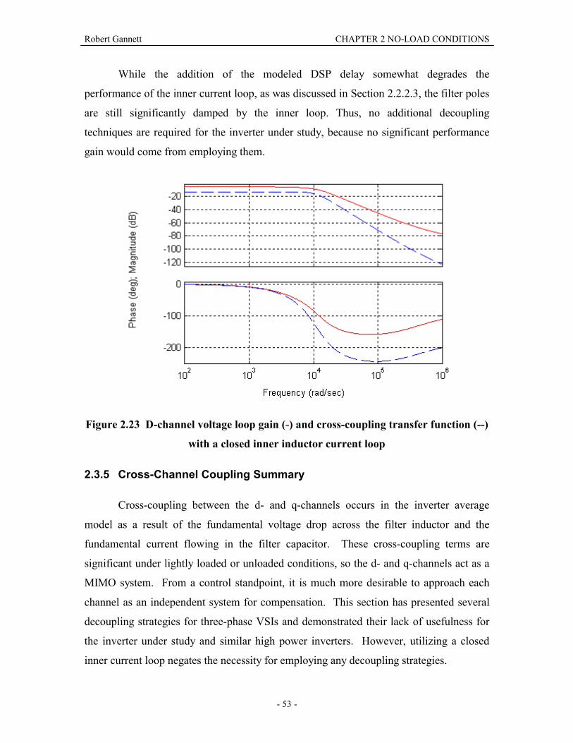
Robert Gannett CHAPTER 2 NO-LOAD CONDITIONS
- 53 -
While the addition of the modeled DSP delay somewhat degrades the
performance of the inner current loop, as was discussed in Section 2.2.2.3, the filter poles
are still significantly damped by the inner loop. Thus, no additional decoupling
techniques are required for the inverter under study, because no significant performance
gain would come from employing them.
Figure 2.23 D-channel voltage loop gain (-) and cross-coupling transfer function (--)
with a closed inner inductor current loop
2.3.5 Cross-Channel Coupling Summary
Cross-coupling between the d- and q-channels occurs in the inverter average
model as a result of the fundamental voltage drop across the filter inductor and the
fundamental current flowing in the filter capacitor. These cross-coupling terms are
significant under lightly loaded or unloaded conditions, so the d- and q-channels act as a
MIMO system. From a control standpoint, it is much more desirable to approach each
channel as an independent system for compensation. This section has presented several
decoupling strategies for three-phase VSIs and demonstrated their lack of usefulness for
the inverter under study and similar high power inverters. However, utilizing a closed
inner current loop negates the necessity for employing any decoupling strategies.

Robert Gannett CHAPTER 2 NO-LOAD CONDITIONS
- 54 -
2.4 No-Load Control Summary
All inverters, regardless of their application, should maintain proper performance
under lightly loaded or unloaded conditions. Nevertheless, no-load conditions pose
interesting problems on the inverter system. No-load stability issues and cross-channel
coupling require special attention and highly influence the final control design.
In general, it is desirable to design the output filter with the resulting parasitic
components as small as possible. However, this causes the filter poles to be nearly
undamped at no-load. This could create system instability if the control bandwidth is
below the resonant frequency. Thus, control measures must be made to ensure that
inverter operation remains stable, even when the output terminals are unterminated.
Cross-coupling the between d- and q-channels at no-load in the rotating
coordinate system causes increased complexity of the plant model. For this reason,
several techniques to decouple the channels have been proposed, yet none seem to
effectively solve the problem.
Just as both issues arise from a single condition, both can be managed through a
single control technique. By closing an inner inductor current loop, the filter poles are
well damped under all loading conditions. In this manner, the inner current loop provides
the possibility for increased control bandwidth and eliminates the need to decouple the d-
and q-channels.

Robert Gannett CHAPTER 3 UNBALANCED LOADING CONDITIONS
- 55 -
3 UNBALANCED LOADING CONDITIONS
Unbalanced loading conditions can occur in power systems for a variety of
reasons. In general, small loads (relative to the power level of the distribution system)
are configured to draw power from only one phase. When several single-phase loads are
placed on a distribution system, then the fluctuating power required from each of these
loads can cause unbalance in the power system. Even for dedicated multiple-phase motor
drives, a significant (up to several percent) imbalance in the phase impedances can exist.
Unbalanced phase loading causes negative sequence and zero sequence (in four-wire
systems) to flow in the power system. For ideal sources and distribution systems this
would not be a problem. However, physical systems, with finite output and transmission
impedances, will experience voltage distortion in the form of phase voltage imbalance
and phase shift due to unbalanced loading. As was described in Section 1.2, unbalanced
voltages can cause malfunction and even failure of power-consuming equipment. Thus,
in inverter-fed power systems, it is the responsibility of the inverter to ensure that certain
tolerances on phase voltage imbalance at the load terminals are met under specified
loading conditions.
3.1 Unbalanced Load Impact on Inverters
3.1.1 Unbalanced Three-Phase Variable Representations
Unbalanced output phase voltages or currents can be symmetrically decomposed
(Appendix B) into their negative sequence and zero sequence components. Figure 3.1
demonstrates this concept for unbalanced output voltages. Note that the zero sequence is
the same for all phases. It is clear that both the negative and zero sequence distortion
occur in the stationary abc reference frame at the fundamental frequency, ω .
Transforming to dqo-coordinates, the negative sequence distortion appears as a
disturbance in the d- and q-variables at a frequency of ω⋅2 . This is the case because the
dq reference frame is rotating in the positive direction at an angular frequency of ω ,
while the negative sequence disturbance rotates at an angular frequency of ω in the
opposite direction. The zero sequence disturbance appears in the o-variable at a

Robert Gannett CHAPTER 3 UNBALANCED LOADING CONDITIONS
- 56 -
frequency of ω , because the o-axis is stationary. Figure 3.2 displays unbalanced output
voltages in the abc reference frame, and their corresponding representation in the dqo
reference frame. Both figures below are simulation plots based on the inverter under
study, with a fundamental output frequency, ω , of 4002 ⋅⋅π rad/sec.
Figure 3.1 Symmetrical decomposition of unbalanced phase a (-), phase b (--), and
phase c (-.) voltages
Figure 3.2 Unbalanced abc-coordinate voltages and their representation in
dqo-coordinates

Robert Gannett CHAPTER 3 UNBALANCED LOADING CONDITIONS
- 57 -
3.1.2 Implications for Control
It is clear from the plots above that unbalanced output currents, as a result of
unbalanced phase loading, will create d- and q-channel load currents that have a ω⋅2
rad/sec sinusoidal disturbance on top of a DC offset. Subsequently, if the d- and q-
channel duty cycles are constant (as is the case for balanced loading), then the sinusoidal
component of the d- and q-channel load currents will flow through the output capacitor,
creating the d- and q-voltage distortion. The o-channel will be similarly affected by the
ω rad/sec disturbance in the o-channel load current.
In order to prevent the sinusoidal current disturbances from causing dqo-voltage
distortion, the sinusoidal currents must not flow through the output capacitors. Thus,
these currents must be delivered by the dqo-channel voltage sources, through sinusoidally
varying duty cycles. The following section solves the steady state equations for the duty
cycles that will provide the appropriate load currents to prevent dqo-channel output
voltage distortion.
3.1.3 Steady State DQO-Channel Solutions
In order to facilitate this discussion, it is necessary to rewrite the d-channel state
space equations in the following form, with the load being an ideal current source input,
[ ] [ ] [ ]
⋅⋅⋅+
⋅−+
⋅=
⋅
⋅⋅−+
⋅
−+
⋅
−−−
=
Cq
LqC
dload
dC
Cd
LdCd
Cq
LqC
dload
d
CDC
Cd
Ld
CL
Cd
Ld
VI
RCID
RVI
RV
VI
LRC
ID
C
LR
LV
VI
C
LLRR
VI
ω
ω
ωω
001
01001
1
,
,
. (3.1)
The q-channel equations will be exactly the same, only with the signs of the cross-
coupling terms reversed. The o-channel equations will also be of the same form, simply
with the cross-coupling terms removed altogether. However, it is important to note that
L in the o-channel will be replaced with the o-channel equivalent inductance,

Robert Gannett CHAPTER 3 UNBALANCED LOADING CONDITIONS
- 58 -
nfilter LL ⋅+ 3 , and LR will be replaced with the o-channel equivalent inductor ESR,
LR⋅2 .
Using these state space equations, it becomes easy to solve for the steady state
dqo-channel conditions. Ideally, at steady state, the dqo-channel output voltages will
track the references perfectly (assuming the Park’s Transformation is aligned with the
line-to-line voltage vectors),
=
−
00
, pkll
o
q
d V
VVV
, (3.2)
where pkllV ,− is the amplitude of the line-to-line output voltage in abc-coordinates. Under
steady state, the dqo-channel output voltages should be unchanging, and therefore the
derivatives of the channel voltages are zero (capacitor currents equal to zero). This
allows the steady state dqo-channel inductor currents to be solved for using the
definitions in (3.2) for the dqo-channel steady state output voltages,
⋅⋅+
=
−
0
0
,
,
,
,
CVIII
III
pkll
oload
qload
dload
Lo
Lq
Ld
ω . (3.3)
Given the state variable definitions at steady state in equations (3.2) and (3.3), the
steady state dqo-channel duty cycles can be solved,
⋅⋅⋅⋅−
⋅+
−⋅⋅+
⋅
⋅+
⋅
⋅+=
−
0
1
02
1
3
12
,,
,
,
,
,
,
,
,
CRCL
VV
II
VL
III
RRR
VIII
dtd
LLLL
VDDD
LDC
pklldload
qload
DCoload
qload
dload
L
L
L
DCoload
qload
dload
nDC
o
q
d
ωω
ω (3.4)
It is interesting to note that under balanced, linear loading, the dqo-channel load
currents will all be constants. Thus, the derivative terms become zero, and the steady
state duty cycles are all constants. However, under unbalanced loading, the dqo-channel
load currents will be sinusoidally varying with DC offsets. Likewise, this will cause the

Robert Gannett CHAPTER 3 UNBALANCED LOADING CONDITIONS
- 59 -
steady state duty cycles to contain a constant component and a sinusoidally varying
component.
3.2 Conventional Solutions
Being a well-known issue in power systems, the problem of unbalanced loading
has been addressed with traditional control strategies. The following section will present
some of these techniques and simulation results from the inverter under study.
3.2.1 Extending Controller Bandwidth
By using some type of integral compensation in the dqo-channels, zero steady
state errors will be achieved for the DC component of the dqo-channel output voltages.
However, as has been demonstrated in the previous sections, an unbalanced load will
cause sinusoidal disturbances in the dqo-channel load currents, and likewise the output
voltages. If a traditional integral controller, as is in Section 2.2.1, with a bandwidth
below the frequency of the disturbances is employed, very little attenuation of the
disturbances over open loop operation will be achieved.
By utilizing controllers with bandwidths greater than the frequency of the
disturbances, some attenuation will be achieved. For example, approximately 20 dB of
attenuation of the disturbance will be achieved if the control bandwidth is a decade above
the disturbance frequency (assuming a 20 dB/dec crossover slope). This may bring the
output distortion within reasonable tolerances, but in order to do so the control bandwidth
would need to be ω⋅⋅102 for the d- and q-channels and ω⋅10 for the o-channel. While
this may be possible in low power inverters, it would be very difficult, and likely
impossible, to accomplish in high power inverters due to the difficulties listed in Section
1.3. The impossibility of this option is amplified for inverters with high output
fundamental frequencies, such as the inverter under study.
3.2.2 Load Current Feedforward Control
Because of the unlikelihood of increasing the controller bandwidth sufficiently to
achieve appropriate performance, other techniques are required to control the
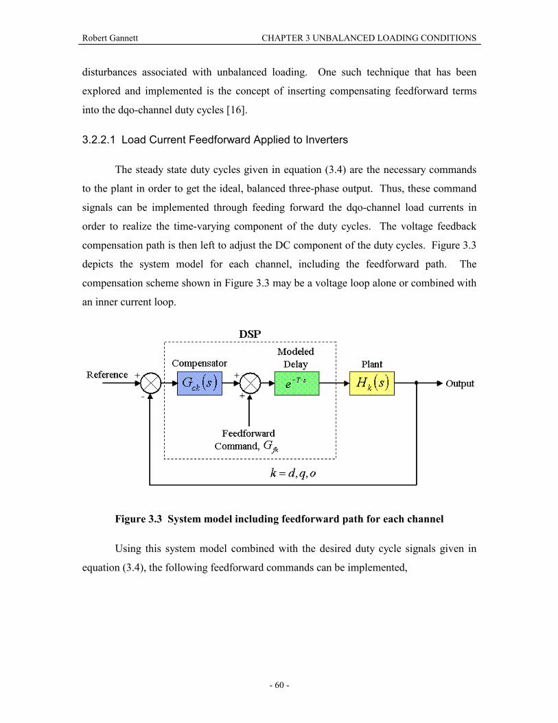
Robert Gannett CHAPTER 3 UNBALANCED LOADING CONDITIONS
- 60 -
disturbances associated with unbalanced loading. One such technique that has been
explored and implemented is the concept of inserting compensating feedforward terms
into the dqo-channel duty cycles [16].
3.2.2.1 Load Current Feedforward Applied to Inverters
The steady state duty cycles given in equation (3.4) are the necessary commands
to the plant in order to get the ideal, balanced three-phase output. Thus, these command
signals can be implemented through feeding forward the dqo-channel load currents in
order to realize the time-varying component of the duty cycles. The voltage feedback
compensation path is then left to adjust the DC component of the duty cycles. Figure 3.3
depicts the system model for each channel, including the feedforward path. The
compensation scheme shown in Figure 3.3 may be a voltage loop alone or combined with
an inner current loop.
Figure 3.3 System model including feedforward path for each channel
Using this system model combined with the desired duty cycle signals given in
equation (3.4), the following feedforward commands can be implemented,

Robert Gannett CHAPTER 3 UNBALANCED LOADING CONDITIONS
- 61 -
( )
⋅⋅+⋅⋅+
⋅⋅+⋅+⋅
⋅⋅−⋅+⋅
⋅=
oloadLoloadn
dloadqloadLqload
qloaddloadLdload
DCfo
fq
fd
IRIdtdLL
ILIRIdtdL
ILIRIdtdL
VGGG
,,
,,,
,,,
23
1 ω
ω
. (3.5)
These feedforward commands will create the necessary time-varying components of the
duty cycle that the low bandwidth compensator will not be able to accomplish. It is also
important to notice that the feedforward commands contain derivatives of the dqo-
channel load currents. As discussed previously, taking a derivative is physically
unrealizable. However, the dqo-channel inductor voltages contain the derivative of the
load currents through the inductor voltage-current relationship, dt
dILV LL = . This works
well for simulation, but unfortunately, the dqo-channel inductor voltage is not a
physically measurable variable. And thus, the derivative of the dqo-channel load currents
must be obtained through some other means or calculation.
It is important to note that load current feedforward is a slight misnomer. True
feedforward assumes that the variables that are fed forward are known and independent
of the controlled system. In the case of the dqo-channel load currents, these two
assumptions are false, because the load currents are closely coupled to the plant state
variables. Thus, as was discussed for decoupling strategies in Section 2.3.3.1, this
feedforward control in fact forms a feedback loop. As a result, the system stability is
affected and must be examined.
3.2.2.2 Load Current Feedforward Control Design
Making use of the previous section, a feedforward controller can be designed for
the inverter under study. Plugging in the physical system parameters for the inverter
under study, equation (3.5) becomes,

Robert Gannett CHAPTER 3 UNBALANCED LOADING CONDITIONS
- 62 -
⋅⋅+⋅⋅
⋅⋅+⋅⋅+⋅⋅
⋅⋅−⋅⋅+⋅⋅
=
−−
−−−
−−−
oloadoload
dloadqloadqload
qloaddloaddload
fo
fq
fd
IIdtd
IIIdtd
IIIdtd
GGG
,5
,7
,4
,5
,8
,4
,5
,8
102.3108.2
107.1106.1107
107.1106.1107
. (3.6)
In order to demonstrate the merits of this control strategy, an unbalanced loading
case must be established. Phase a and b are loaded to full rated power, and phase c is
loaded to 85% of full rated power (specification for inverter under study). Figure 3.4
shows the output voltages for the inverter under study operating with a low bandwidth
controller and under the loading conditions described above. A line depicting the
nominal peak voltage of 162.6 V (for 115 Vrms) has been provided for reference. Using
the low bandwidth controller alone under the unbalanced loading conditions results in
significant disturbances in the dqo-channel output voltages. Consequently, the output
voltages in abc-coordinates are unbalanced. The output has a maximum phase unbalance
of 4.2%, with a maximum difference of 8.5 V between phases. Figure 3.5 shows the
result of adding the feedforward commands, as portrayed in equation (3.6). Using the
feedforward commands, as predicted, results in perfect dqo-channel output voltages, and
likewise, abc-coordinate output voltages with no unbalance.
The results in Figure 3.5 are without the addition of the modeled DSP delay in the
control loop. When the delay is included, the system becomes unstable, because the
feedforward control is in actuality a feedback loop. If the feedforward terms were
independent variables, their future values could be predicted and the effects of the phase
lag could be minimized. However, because the feedforward terms here are closely
coupled to the state variables, accurate prediction is unlikely, and impossible in the case
of transient situations. In order to stabilize the system for this case, the feedforward path
gains must be decreased. Figure 3.6 shows the results when the modeled delay is
included and the feedforward gains are decreased by 50%. The consequence of
decreasing the gains is quite evident in the substantially reduced performance. The abc-
coordinate outputs in figure 3.6 have a maximum phase unbalance of 2.4% with a
maximum difference of 4.7 V between the phases.

Robert Gannett CHAPTER 3 UNBALANCED LOADING CONDITIONS
- 63 -
Figure 3.4 Phase a (-), phase b (--), and phase c (-.) output voltages under
unbalanced load
Figure 3.5 Phase a (-), phase b (--), and phase c (-.) output voltages under
unbalanced load with load current feedforward

Robert Gannett CHAPTER 3 UNBALANCED LOADING CONDITIONS
- 64 -
Figure 3.6 Phase a (-), phase b (--), and phase c (-.) output voltages under
unbalanced load with modeled delay and decreased feedforward gains
3.2.2.3 Load Current Feedforward Control Analysis
For a perfect plant model and no control delay, load current feedforward
completely compensates for the unbalanced load currents. However under realistic
situations, the performance of this technique is significantly degraded. The delay in the
system necessitates decreasing the gains of the feedforward controller, diminishing its
effectiveness. In addition, the feedforward control relies on accurate knowledge of the
physical plant parameters, L and LR , in order to produce the command that will give
ideal outputs. Perfect knowledge of these parameters, though, is not realistic, and thus
further degradation of the feedforward controller may occur. In fact, these parameters
may even be time-varying by 25% or more due to magnetic saturation and temperature
drift.
Even though the load current feedforward control does realize some increase in
performance under realistic conditions over the low bandwidth controller, the output
voltages are likely still to be out of specifications. For the inverter under study, the

Robert Gannett CHAPTER 3 UNBALANCED LOADING CONDITIONS
- 65 -
output voltage unbalance, as seen in Figure 3.6, is still over 2 %. Thus, load current
feedforward may not a viable option for unbalanced loading compensation for high
power inverter applications.
3.3 Proposed Solution
In light of the poor and unacceptable performance of the conventional solutions to
unbalanced loading, new techniques are required to compensate for unbalanced loading
in high power inverter applications. This section will present a feedback control strategy
for high power three- and four-leg inverters under unbalanced loading conditions.
3.3.1 Motivations
The feedforward technique described above sought to compensate for the dqo-
channel disturbances, due to unbalanced loading, by injecting sinusoidal terms into the
channel duty cycles based on the negative and zero sequence components of the load
currents. Another approach to the problem of unbalanced loading is to inject
compensating terms into the duty cycles based on the negative and zero sequence content
of the output voltages. While the first technique works perfectly when the knowledge of
the plant is perfect, the latter technique does not require knowledge of the plant to work
perfectly, because it is a true feedback of the variable of interest. Ultimately,
feedforward control does not succeed because it does not make adjustments based on the
variable which it is attempting to correct.
The steady state error of a feedforward controller is determined by the accuracy of
the feedforward path gains (with respect to the physical plant parameters) and the delay
in the control loop. However, a feedback controller’s steady state error is determined by
the loop gain at the frequency of interest. In the case of DC quantities, a feedback
controller can, in fact, achieve zero steady state errors by using an integrator, whose DC
gain is infinite. This fact creates the motivation for developing a feedback controller to
deal with unbalanced loading.

Robert Gannett CHAPTER 3 UNBALANCED LOADING CONDITIONS
- 66 -
3.3.2 Negative Sequence Controllers in Three-Leg Inverters
In three-phase, three-wire systems (delta connected sources and loads),
unbalanced loads create negative sequence currents, and likewise, negative sequence
voltage distortion. A previously unexplored control technique has been proposed in
literature [24] to compensate for the negative sequence voltage distortion due to
unbalanced loads in three-phase, three-wire systems. In traditional control of three-phase
inverters, a rotating dq reference frame is established, such that the time-varying output
voltages are transformed into DC quantities. This enables perfect tracking of the
reference for the positive sequence component of the output voltage. Hsu and Behnke
[24] propose the construction of a reference frame rotating at the fundamental frequency
in the opposite direction as the positive sequence. Thus, the negative sequence
components of the output voltage will become DC quantities in this negative sequence dq
reference frame. With a parallel controller in the negative sequence dq reference frame,
the negative sequence distortion can be attenuated, or even eliminated if an integral
controller is used. Hsu and Behnke [24] have demonstrated this concept in simulation and
experimentation, with the predicted results.
The proposed control scheme above is quite effective for three-phase, three-wire
systems; however, many loads require a fourth (neutral) connection. This control
strategy could effectively eliminate the negative sequence distortion in four-wire systems,
but it would not address the issue of zero sequence distortion. As a result, this technique
alone would not suffice for control of three-phase, four-leg inverters.
3.3.3 Negative and Zero Sequence Controllers in Four-Leg Inverters
Because a voltage feedback scheme has been demonstrated to eliminate steady
state negative sequence errors in thee-leg inverters, it is only logical to believe that a
similar scheme can be applied to four-leg inverters to eliminate both negative and zero
sequence steady state errors. This possibility is described and demonstrated through
simulation in the following sections.

Robert Gannett CHAPTER 3 UNBALANCED LOADING CONDITIONS
- 67 -
3.3.3.1 Unbalanced Load Control Concept
3.3.3.1.1 Negative Sequence Controller
The concept of the negative sequence controller in the context of four-leg
inverters is the same as described above for a three-leg inverter. The negative sequence
distortion caused by an unbalanced load can be transformed into DC quantities through a
change of basis to a reference frame rotating in the negative (clockwise) direction at the
fundamental frequency. Then, an integrator can operate on the negative sequence error
signal and the resulting output, transformed back to the positive sequence frame, to be
added to the dq-channel duty cycles. The resulting compensation will achieve zero
steady state errors for the negative sequence distortion. Figure 3.7 displays this control
strategy in block diagram format.
Figure 3.7 Negative sequence control structure
It is interesting to note that positive sequence component of the output voltage
will appear in dV− and qV− as a sinusoid at a frequency of ω⋅2 . Thus, the authors of
[24] have suggested that the negative sequence d and q references should be the
transformation of the positive sequence d and q references into the negative sequence
rotating frame, given by,

Robert Gannett CHAPTER 3 UNBALANCED LOADING CONDITIONS
- 68 -
( )( )
⋅⋅−⋅⋅
=
−
−
−
−
ωω
2sin2cos
,
,
pkll
pkll
q
d
VV
RR
. (3.7)
These references are redundant and unnecessary, assuming that the bandwidth of the
negative sequence controllers is sufficiently low. It is the responsibility of the positive
sequence controllers to ensure that the positive sequence references are followed
precisely. The negative sequence controllers should only operate on the DC components
of the negative sequence d- and q-voltages, and ensure they are exactly zero. Thus the
negative sequence d and q references can simply be zero. It is then required that the
bandwidth of this negative sequence controller is less than ω⋅2 , so that it does not try to
attenuate the positive sequence voltages’ presence in the negative rotating frame. If the
bandwidth of the negative sequence controller approaches ω⋅2 , then the references
given in (3.7) must be used to ensure that the negative sequence controller does not give
conflicting commands with the fundamental positive sequence controller.
3.3.3.1.2 Zero Sequence Controller
The fourth leg of the inverter facilitates control of the zero sequence current, and
likewise, the zero sequence voltage distortion. As was described in Section 3.1.1, the
zero sequence voltage distortion appears as a disturbance in the o-channel at the
fundamental frequency. Because the o-axis actually exists in the stationary frame (see
Appendix A), there is no way to rotate the o-channel voltage in order to transform it into
a DC quantity. Thus, some other technique must be employed to attenuate the o-channel
disturbance.
In order to achieve zero steady state errors for a frequency of interest, the loop
gain must be infinite at that frequency. This is easily accomplished for DC with an
integrator. However, in order to achieve a loop gain of infinity at other frequencies a
zero-damping bandpass filter must be employed. The transfer function for a zero-
damping bandpass filter is given in equation (3.8). Figure 3.8 displays the Bode
diagrams for a zero-damping bandpass filter with a resonant frequency arbitrarily chosen
to be 1000 rad/sec.

Robert Gannett CHAPTER 3 UNBALANCED LOADING CONDITIONS
- 69 -
( ) 2
2
1
+
=
o
oBP
s
s
sG
ω
ω (3.8)
Figure 3.8 Bode diagrams of a zero-damping bandpass filter
The Bode diagram above does not show an infinite gain at the resonant frequency
due to rounding in the solver. Nevertheless, it is clear from equation (3.8) that as
ojs ω→ , the denominator will approach zero, and thus the magnitude of the transfer
function will approach infinity.
Using a zero-damping bandpass filter, it is clear that an infinite gain can be
obtained for a discrete frequency. Thus, by placing a parallel path in the o-channel,
containing a zero-damping bandpass filter with a resonant frequency of ω , the loop gain
will be infinite at the zero sequence disturbance frequency. This will make zero steady
state errors possible for the zero sequence distortion from unbalanced loads. Figure 3.9
displays a block diagram of the zero sequence controller described above. Because the o-
axis is the same in all rotating reference frames, this o-channel zero sequence controller
can be implemented in any dqo reference frame. For simplicity, it has been shown here

Robert Gannett CHAPTER 3 UNBALANCED LOADING CONDITIONS
- 70 -
in the fundamental frequency positive rotating frame, where traditional fundamental
compensation is performed. The fundamental compensation blocks in Figure 3.9 may
also contain an inner current loop. The positive sequence references do not change from
traditional dqo-channel control,
=
−
00
, pkll
o
q
d V
RRR
. (3.9)
Figure 3.9 Zero sequence controller structure
3.3.3.1.3 Complete Unbalanced Load Controller
Combining the negative sequence and zero sequence controllers described above
will result in zero steady state errors for both the negative and zero sequences under
unbalanced loading conditions. This leaves only the positive sequence, controlled by the
fundamental controllers, resulting in a perfect three-phase output in abc coordinates.
A minor simplification in error signal calculation can be made when several
rotating reference frames are used in control. Rather than transforming the abc output
voltages into several equivalent rotating dq voltages, the abc output voltages can be

Robert Gannett CHAPTER 3 UNBALANCED LOADING CONDITIONS
- 71 -
subtracted from ideal abc-coordinate references, and the abc error signals can then be
transformed into the rotating reference frames. This is a minor simplification that may or
may not achieve some benefit in actual implementation. Figure 3.10 depicts the complete
unbalanced control strategy as expressed above. The abc references are given by the
ideal output,
( )
⋅+⋅⋅
⋅−⋅⋅
⋅⋅
=
−
−
−
32sin
32sin
sin
,
,
,
πω
πω
ω
tV
tV
tV
RRR
pkll
pkll
pkll
c
b
a
. (3.10)
Figure 3.10 Complete unbalanced load control structure
3.3.3.2 Unbalanced Load Control Design
Using the control structure of Figure 3.10, an unbalanced load controller can be
designed for the inverter under study. The fundamental compensators will be the same as

Robert Gannett CHAPTER 3 UNBALANCED LOADING CONDITIONS
- 72 -
described in Figure 2.14 and Table 2.2, with an inner current loop to dampen the output
filter poles at light load. Consequently, the dynamics of the system, with respect to the
fundamental positive sequence, will be identical to the no-load control scheme as
described in Section 2.2.2. Table 3.1 lists the integrator gains for the negative sequence
controllers and the transfer function for the zero sequence controller. The integrator
gains haven been chosen under the guidelines given in 2.2.1.1 for conventional voltage
loop compensation. Because the dqo average model of the inverter is the same in both
the positive and negative fundamental rotating reference frame, the designed integral
gains are the same. While this ensures that the negative sequence control is stable alone,
it does not ensure that the entire control system is stable. This topic will be discussed in
more detail in the next section. In order to ensure convergence of the simulation package
solver, a small amount of damping has been added to the bandpass filter transfer function
for the zero sequence controller.
Table 3.1 Unbalanced Load Controller Parameters
Parameter ValueG-id 0.16G-iq 0.16
( )sGBPo( )
( )2
2
2
40024002001.01
4002
⋅⋅+
⋅⋅⋅+
⋅⋅
ππ
πss
s
Using the parameters displayed above, Figure 3.11 gives the results for the
inverter under study with an unbalanced load (100%-100%-85% phase loading) and
modeled DSP delay. There is a maximum phase voltage unbalance of 0.23% and a
maximum difference between phases of 0.45 V. Zero steady state errors have not truly
been reached, because of the damping added to the bandpass filter and rounding errors in
the solver (see discussion of Figure 3.9 above).
In order to show the transient response of the unbalance controllers, Figure 3.12
has been provided below. This figure displays the d- and q-component of the abc-

Robert Gannett CHAPTER 3 UNBALANCED LOADING CONDITIONS
- 73 -
coordinate error signal in the negative sequence (a), and the zero sequence component of
the error signal (b). The controllers have been turned on at a time of 100 milliseconds. It
is clear that the error signals converge toward zero over several 400 Hz line cycles. The
speed of response for the negative sequence controller is similar to that for the
conventional voltage loop control, described in Section 2.2.1, because the integrator gains
are the same. There is some distortion present in the negative sequence d- and q-channels
in Figure 3.12. This is an artifact of the implementation of the transformation between
abc- and dqo-coordinates. The true transformation is a continuous-time function,
however, the implementation in simulation operates on discrete time steps. This fact
combined with rounding errors contributes to the distortion seen in Figure 3.12. It is
important to note that the distortion is present before the controllers are turned on, and
their presence does not contribute to the distortion.
Figure 3.11 Phase a (-), phase b (--), and phase c (-.) output voltages under
unbalanced load with proposed controller

Robert Gannett CHAPTER 3 UNBALANCED LOADING CONDITIONS
- 74 -
(a)
(b)
Figure 3.12 (a) Negative sequence controller transient response for the d- and q-
channels; (b) Zero sequence controller transient response
3.3.3.3 Stability Analysis
As with any control system design, it is of utmost importance to ensure stable
operation of the controlled system. Thus, some strategy to test the stability of the system
must be employed, regardless of the fact that parallel controllers are operating in different
rotating reference frames. This issue has been addressed in literature [25] through the
development of a transformation for regulators in a rotating reference frame to their
stationary reference frame equivalent. A rotating reference frame regulator, ( )sGrf , is
represented in the stationary frame by,
( ) ( ) ( )[ ]rrfrrfsf jsHjsHsG ωω ⋅−+⋅+⋅=21 , (3.11)

Robert Gannett CHAPTER 3 UNBALANCED LOADING CONDITIONS
- 75 -
where rω is the angular rotation frequency of the reference frame. While this is the
precise transformation, it is difficult to physically realize. For this reason, Zmood and
Holmes [25] have proposed the following simplification of equation (3.11):
( )
⋅+
=s
sGsG rrfsf 2
22 ω . (3.12)
Using this transformation for an integral controller, ( )s
KsG irf = , in the rotating reference
frame yields,
( ) 22
2
r
isf s
sKsG
ω+⋅⋅
= , (3.13)
in the stationary frame. Equation (3.13) is clearly a zero damping bandpass filter
centered at the frequency rω . It is interesting to note that both the positive and negative
sequence controllers will map into the same frequency in the stationary frame. For this
reason, the two controllers are represented by a single bandpass filter in the αβ
stationary frame, as depicted in Figure 3.13. This initial analysis indicates that
appropriate stability margins are maintained when both the positive and negative
sequence controllers are represented in the same reference frame. The high loop gain at
400 Hz will ensure that the fundamental component of the reference will be tracked with
near zero steady state errors.
Because the o-channel already exists in the stationary frame, no transformation of
the regulator is required. Figure 3.14 displays the o-channel loop gain with the zero
sequence controller included. From this figure, initial analysis of the o-channel controller
points toward a stable closed loop system. It is interesting to note the interaction between
the fundamental control and the zero damping bandpass filter cause a sharp notch in the
loop gain below the resonant frequency of the bandpass filter. This does not, however,
significantly affect the o-channel bandwidth (for comparison see Figure 2.15). Both
figures below are obtained under light loading conditions, where the filter peaking is
most significant.

Robert Gannett CHAPTER 3 UNBALANCED LOADING CONDITIONS
- 76 -
Figure 3.13 Stationary frame (alpha/beta) loop gain for unbalance control with
modeled digital delay
Figure 3.14 O-channel loop gain for unbalance control with modeled digital delay
3.3.3.4 Unbalanced Load Control Design Analysis
By utilizing negative and zero sequence controllers, near zero steady state errors
can be achieved for the output phase voltages under unbalanced loading conditions. By

Robert Gannett CHAPTER 3 UNBALANCED LOADING CONDITIONS
- 77 -
rotating the error signal into the fundamental frequency negative sequence, the negative
sequence distortion is transformed into DC quantities. This enables traditional DC
control techniques to be employed, and thus the possibility of eliminating steady state
errors to be realized. Combined with a zero damping bandpass filter (infinite gain at
resonant frequency) to compensate for zero sequence distortion, excellent inverter
performance under unbalanced loading is enabled.
Because this technique should achieve near zero steady state errors, then even
under the harshest of unbalances, the output should remain well regulated. This worst
case unbalance occurs when one or two phases is unterminated, while the other(s) is(are)
fully loaded. This could, in fact, happen if each output phase has independent circuit
breakers or fuses. Simulation of this loading case reveals that the controllers maintain
regulation of all phases within 1.6% of the nominal output voltage for the inverter under
study, thereby proving the operation of this control strategy.
It is important to also note the transient behavior of the unbalance controllers.
While steady state performance may achieve near zero steady state errors; under
transients, the controllers may require several line cycles to reach a steady state. This is
due to the choice of bandwidth of the controllers to be much smaller than the
fundamental control bandwidth. Thus, the tracking performance of these controllers will
be degraded if the unbalanced load is not slowly time-varying.
The control structure described in this section will unavoidably require additional
processing time due to the error signal being rotated into an additional reference frame.
However, because high power switching devices require such low switching frequencies,
in comparison to the processor speeds of modern DSPs, there will likely be enough time
to make all of the necessary transformations and calculations within one power stage
switching period.
3.4 Unbalanced Load Control Summary
In three-phase VSI control, the d- and q-channels are used to compensate for the
rotating components (positive and negative sequence) of the output variables (voltage and

Robert Gannett CHAPTER 3 UNBALANCED LOADING CONDITIONS
- 78 -
current). When conventional voltage loop compensation is utilized in the fundamental
positive sequence reference frame, it is generally not possible to achieve a bandwidth
high enough, in high power VSIs, to attenuate the disturbances due to unbalanced loads.
When a fourth leg is included in the VSI, an additional channel, the o-channel, is
introduced to compensate for the stationary (zero sequence) component of the output
variables. One of the foremost reasons that a fourth-leg has been proposed for VSIs, is to
be able to control the zero sequence current present when three-phase loads require a
fourth (neutral) connection. Again, using conventional voltage loop compensation in the
o-channel does not facilitate a high enough bandwidth to attenuate the zero sequence
disturbance due to unbalanced loads.
Because of traditional control’s inability to compensate for unbalanced loading
conditions, special techniques have been proposed to achieve acceptable output
performance. Load current feedforward techniques have been shown to eliminate all
output voltage error when an ideal physical system is used. However, under realistic
conditions and control delay, the performance of the feedforward technique is
significantly reduced. Hsu and Behnke [24] have proposed and demonstrated a negative
sequence controller to eliminate negative sequence distortion in three-phase, three-wire
power systems. This technique can be applied similarly to three-phase, four-wire VSIs;
however, it does nothing to address zero sequence distortion. A zero damping bandpass
filter for compensation of zero sequence disturbances due to unbalanced loading has been
proposed and simulated in this thesis. Table 3.2 and Table 3.3 below display the
performance of the control strategies described above compared to open loop operation
under two separate loading conditions, 100%-100%-85% phase loading and 100%-100%-
0% phase loading.

Robert Gannett CHAPTER 3 UNBALANCED LOADING CONDITIONS
- 79 -
Table 3.2 Comparison of Control Techniques under Moderate Unbalance
Open Loop Fundamental Control
Feedforward Control
Negative and Zero Sequence Control
max. % difference from
nominal3.76% 4.24% 2.39% 0.23%
max. voltage difference between phases
7.78 V 8.50 V 4.67 V 0.45 V
Table 3.3 Comparison of Control Techniques under Severe Unbalance
Open Loop Fundamental Control
Feedforward Control
Negative and Zero Sequence Control
max. % difference from
nominal27.13% 37.50% 24.12% 1.61%
max. voltage difference between phases
59.58 V 74.67 V 53.19 V 3.01 V
From these tables, it is clear that the control structure proposed in Section 3.3 far
exceeds the performance of the other control schemes. Moreover, the proposed controller
performs better under the most severe unbalance than the feedforward control does under
just moderate unbalance. These results demonstrate the true merit of the proposed
control structure.

Robert Gannett CHAPTER 4 NON-LINEAR LOADING CONDITIONS
- 80 -
4 NON-LINEAR LOADING CONDITIONS
With the increasing prevalence of electronic loads in today’s world, non-linear
loading is becoming more of a problem in power systems. The most common non-linear
loads are three-phase and single-phase rectifiers. Both of these types of loads draw
harmonic currents from the source. Harmonic voltage distortion occurs when these
currents flow through the finite output and transmission impedances of the power system.
Harmonic distortion can be extremely damaging to loads and power transmission
equipment, such as transformers. For this reason, THD guidelines have been established
for power systems to prevent improper operation of, or damage to, power-processing and
power-consuming equipment. Nevertheless, reducing harmonic distortion in high power
systems is not a trivial task, and has become a topic of a great amount of research in
recent years. This chapter will present the results of some of this research and as well as
some new techniques to attenuate harmonic distortion in inverter-fed power systems.
4.1 Non-Linear Load Impact on Inverters
This section will specifically describe the impact of three-phase and single-phase
diode rectifiers on inverter-fed power system. While these are not the only types of non-
linear loads, they do represent the majority, and their characteristics may be
representative of other types of non-linear loads.
4.1.1 Three-Phase Diode Rectifiers
Three-phase diode rectifiers are used in a wide variety of applications, such as
front-end converters for DC distribution systems and motor drives. In general, three-
phase diode rectifiers are used in medium to high power (> 1 kVA) AC/DC converter
applications. Figure 4.1 displays a schematic of a three-phase diode rectifier. The
resistive load may also be accompanied by some filtering elements.

Robert Gannett CHAPTER 4 NON-LINEAR LOADING CONDITIONS
- 81 -
Figure 4.1 Three-phase diode rectifier
4.1.1.1 Harmonic Distortion
A three-phase diode rectifier is an uncontrolled, six-pulse converter, whose
switches turn on and off based on the relative magnitudes and phases of the input lines.
Thus, an ideal three-phase rectifier will only draw currents at the following harmonic
frequencies:
( )[ ] ω⋅±⋅ 16 n , (4.1)
where n is any positive, real integer and ω is the fundamental line frequency. A property
of three-phase diode rectifiers is that all ( )[ ] ω⋅+⋅ 16 n harmonic currents are positive
sequence, and all ( )[ ] ω⋅−⋅ 16 n harmonic currents are negative sequence (Appendix C
mathematically demonstrates this property). These currents will cause harmonic voltage
distortion at the same frequencies in the same rotating direction. From Figure 4.1, it is
clear that there is no neutral connection, and thus no zero sequence current or distortion
will be present.
Figure 4.2 and 4.3 below display the output phase voltage distortion in the time
and frequency domains for the inverter under study in open loop operation with a full
three-phase non-linear load (90 kVA) of the configuration shown in Figure 4.1. It is
interesting to note that the magnitude of the harmonic voltage distortion decreases as the

Robert Gannett CHAPTER 4 NON-LINEAR LOADING CONDITIONS
- 82 -
frequency increases. The reason for this is twofold. First, a Fourier analysis of the phase
currents reveals that the lower frequency harmonics are dominant; and secondly, the
output impedance of the inverter generally decreases with increasing frequency
(characteristic of LC low-pass filter).
Figure 4.2 Output phase voltage (-) and current (--) under 90 kVA three-phase
diode rectifier
Figure 4.3 Frequency components of the output phase voltage under 90 kVA three-
phase diode rectifier

Robert Gannett CHAPTER 4 NON-LINEAR LOADING CONDITIONS
- 83 -
4.1.1.2 Implications for Control
From the plots above, it is clear that the output phase voltages are highly distorted
by heavy three-phase diode rectifier loading. In the case of the inverter under study the
THD is over 20%. It is important to note that the majority of the distortion is contained
in the 5th and 7th harmonics, because the output filter attenuates the higher frequency
harmonics. Therefore, additional means must be employed to attenuate the lower
frequency harmonics.
Because the 5th harmonic distortion rotates in the negative sequence and the 7th
rotates in the positive sequence, both will appear as disturbances in the d- and q-voltages.
In fact, both harmonics will emerge as disturbances at a frequency of ω⋅6 in the d- and
q-voltages. This occurs because the 5th harmonic disturbance is rotating in the opposite
direction of the fundamental rotating reference frame, and the 7th harmonic is rotating in
the same direction. As a result, the d- and q-channel loop gains would need to have a
significant magnitude at a frequency of ω⋅6 in order to be able to attenuate these
disturbances. This is impossible in high power inverters, where the switching frequency
is significantly limited by today’s power devices.
4.1.2 Single-Phase Diode Rectifiers
Single-phase diode rectifiers are often used in lower power (< 500 VA) AC/DC
applications. Almost all small electronic equipment and consumer electronic equipment
contain single-phase diode rectifiers. While single-phase diode rectifiers may each only
be used for small power applications, their effects are additive when several draw power
from the same phase. The single phase diode rectifier used for the purpose of simulation
is depicted in Figure 4.4. Additional configurations include other half- and full-wave
rectifiers, with and without filtering.

Robert Gannett CHAPTER 4 NON-LINEAR LOADING CONDITIONS
- 84 -
Figure 4.4 Single-phase diode rectifier used in simulations
4.1.2.1 Harmonic Distortion
Single-phase diode rectifiers are uncontrolled AC/DC converters with either one
or two pulses per line period. An ideal single-phase diode rectifier, configured as in
Figure 4.4, draws currents at all odd harmonic frequencies. As with three-phase
rectifiers, all ( )[ ] ω⋅+⋅ 16 n frequencies are positive sequence, and all ( )[ ] ω⋅−⋅ 16 n
frequencies rotate in the negative sequence. However the odd triplen harmonics (3rd, 9th,
15th, etc.) are zero sequence currents, because their magnitudes do not cancel in the
neutral conductor. Appendix C mathematically details these characteristics of single-
phase diode rectifiers. The harmonic currents drawn by these loads will cause voltage
distortion at the same frequency in the same sequence. All full-wave rectifiers will
exhibit similar characteristics; however, half-wave rectifiers, draw even harmonics, and
will not be discussed in any further detail here. They are rarely used, and only in very
low power applications, so their impact on high power inverters would likely be minimal.
Figure 4.5 and 4.6 display the output phase distortion and the phase and neutral
currents for the inverter under study in open loop operation with a full load of balanced
single-phase diode rectifiers (30 kVA per phase). For an unbalanced load of single-phase
rectifiers, there will also be negative and zero sequence distortion at the fundamental

Robert Gannett CHAPTER 4 NON-LINEAR LOADING CONDITIONS
- 85 -
frequency. As described above for three-phase rectifiers, the magnitude of the harmonic
distortion decreases as the harmonic frequency increases.
Figure 4.5 Output phase voltage (-) and current (--), and neutral current (-.) under
90 kVA single-phase balanced diode rectifiers
Figure 4.6 Frequency components of the output phase voltage under 90 kVA single-
phase balanced diode rectifiers

Robert Gannett CHAPTER 4 NON-LINEAR LOADING CONDITIONS
- 86 -
4.1.2.2 Implications for Control
The output phase voltages are visibly distorted, here with a THD greater than
10%, under single-phase diode rectifier loading. The dominant harmonics are the 3rd, 5th,
and 7th. These three frequencies are not significantly attenuated by the output filter, and
must be alternatively decreased in order to achieve acceptable inverter performance.
As described above in section 4.1.1.2, the negative sequence 5th harmonic and
positive sequence 7th harmonic distortion will both appear as a 6th harmonic disturbance
in the d- and q-voltages. Likewise, all higher frequency ( )[ ] ω⋅−⋅ 16 n and ( )[ ] ω⋅+⋅ 16 n
harmonics will appear together as a corresponding ( ) ω⋅⋅ n6 disturbance in the
fundamental, positive sequence dq reference frame. All of the triplen harmonics exist as
zero sequence distortion (stationary disturbances), and thus will appear in the o-voltage at
the same frequency. As detailed in the sections and chapters above, it is impossible in
high power inverters to achieve a high enough control bandwidth to appreciably reduce
harmonics at these frequencies.
4.2 Conventional Solutions
Because of the ever-growing use of electronic and non-linear loads, harmonic
distortion has become a major consideration in power systems. In the past, many
strategies have been employed to reduce harmonic distortion for specific applications;
however, all have had significant drawbacks. This section will detail some of these
conventional solutions to deal with the effects of distorting loads in three-phase, inverter-
fed power systems.
4.2.1 Passive Filtering
The most common and simplest solution to reduce the harmonic voltage distortion
is through passive filtering at the output terminals of the inverter. This technique seeks to
reduce the output impedance of the inverter at the harmonic frequencies, thereby
reducing the voltage distortion for a given harmonic current magnitude. For example,
decreasing the resonant frequency of the single-stage output filter will reduce the output

Robert Gannett CHAPTER 4 NON-LINEAR LOADING CONDITIONS
- 87 -
impedance of the inverter under study at harmonic frequencies. However, reducing the
resonant frequency of the output filter will require the use of larger passive elements.
This is obviously undesirable from a cost and size/weight standpoint. This technique is
further limited because the resonant frequency can only be decreased to a range
approaching the fundamental frequency. If the resonant frequency is further reduced,
then the filter will attenuate the fundamental output.
Another passive filtering technique is to add harmonic traps to the output filter at
the specific harmonic frequencies where distortion occurs. Harmonic traps will
significantly reduce the output impedance of inverter at the resonant frequency of the
trap; however, harmonic traps have several drawbacks. Care must be taken when using
harmonic traps, because they can cause interactions that may significantly alter the
characteristics of the output filter and actually increase the output impedance at certain
frequencies. Usually harmonic traps require some amount of damping in order to reduce
these interactions. This increases the losses in the trap, thereby decreasing efficiency and
increasing cooling requirements. In addition, harmonic traps tuned to lower frequency
harmonics have very large and expensive passive components. Another limitation of this
technique, is that the harmonic trap must be tuned very accurately, or its effectiveness
will be considerably decreased in reducing the harmonic distortion at the frequency of
interest.
4.2.2 Assistant Inverter and Active Filtering
A topic of particular interest in the power quality field over the last several
decades has been active power filtering. Active power filters have been proposed and
implemented to correct power quality issues, such as unbalance and harmonic distortion.
Active power filters operate on the principle that distortion can be canceled through the
injection of equal but opposite distortion [26]. Essentially, an active filter is just an
inverter controlled to output voltages or currents at harmonic frequencies. Because active
power filters are simply power converters connected in parallel with the power system
loads, they can easily be applied to existing power systems. Figure 4.7 displays an active
filter configuration in a three-phase, four-wire power network. Active power filtering can

Robert Gannett CHAPTER 4 NON-LINEAR LOADING CONDITIONS
- 88 -
also be applied to single-phase and other multi-phase systems, making them an extremely
flexible solution for networks with power quality problems.
Figure 4.7 Active power filter configuration in a three-phase, four-wire power
system
While an active power filter is designed for application to existing power systems,
an assistant inverter is designed specifically to accompany a main inverter in an inverter-
fed power system. The main inverter supplies all of the power at the fundamental
frequency, and the assistant inverter supplies currents at the harmonic frequencies. The
assistant inverter delivers much less power than the main inverter, and consequently the
assistant inverter switching frequency can be much greater, enabling the control of higher
frequency harmonics. Because the assistant inverter sources all of the harmonic current
required by the load, the harmonic currents will not flow through the output impedance of
the main inverter, and thus ideally no voltage distortion will exist at the output of the
main inverter. This, in effect, reduces the output impedance of the inverter to zero at the
specified harmonic frequencies. The design and implementation of an assistant inverter,
as well as experimental results, have been detailed in [16].
While active power filters and assistant inverters have been shown to be
extremely flexible and effective at correcting voltage distortion, they have several

Robert Gannett CHAPTER 4 NON-LINEAR LOADING CONDITIONS
- 89 -
drawbacks. The most obvious is that the additional hardware will add cost and size to the
power system. Overall system efficiency will also be decreased, due to the losses
incurred in the active filter.
4.2.3 Parallel Inverter Operation
Another proposed solution to the problem of distortion in inverter-fed power
systems is the paralleling of inverters. The outputs of the N number of parallel inverters
are controlled to be phase shifted in a manner to achieve current ripple cancellation in the
output filter capacitors. In this fashion, the effective switching frequency of the entire
system is increased N times, as is the effective control bandwidth of the entire system.
Figure 4.8 depicts the simulation results of paralleling 16 models of the inverter under
study with a full three-phase diode rectifier load. This increases the effective switching
frequency and the effective system control bandwidth by 16 times, enabling the
controllers to attenuate the output distortion. The result is an output THD of less than
4%.
Figure 4.8 Output phase voltage for 16 parallel operating models of the inverter
under study

Robert Gannett CHAPTER 4 NON-LINEAR LOADING CONDITIONS
- 90 -
In addition to enabling the attenuation of output harmonics, the paralleling of
inverters adds redundancy to the system. If one of the inverters fails, the output power of
the system is only reduced by the fraction N
N 1− . Although paralleling inverters appears,
on the surface, to be a very convenient solution, it is not without its own disadvantages.
If neither the inputs (DC power sources) nor the outputs of the inverters are isolated, then
small variations in the parallel inverters will cause circulating zero sequence current
between the inverters [27]. While isolating either the DC or AC side of the inverter
prevents this problem, it is expensive and not very practical, especially when a large
number of inverters are to be paralleled. For this reason, zero-sequence current control
has been proposed and simulated for non-isolated parallel inverters [28]. Even in this
case, the size and cost of several smaller inverters combined (16 in the case for the
inverter under study) will almost undoubtedly be greater than the size and cost of one
larger inverter. Despite this possibility of operating non-isolated inverters in parallel, the
increased system and control complexity is not warranted if a simpler solution is
available.
4.3 Proposed Solution
While the conventional solutions to harmonic distortion in power systems may
achieve acceptable power quality, their implementation tends to be costly and
inconvenient because of the added hardware. This section will present and show
simulation results for a new control scheme to attenuate harmonic distortion in three-
phase, four-leg inverters.
4.3.1 Motivations
Because all of the conventional solutions to distortion in power systems have the
disadvantage of requiring additional hardware, it is desirable to develop a control
algorithm to deal with the harmonic distortion. While it is obvious that conventional
control will not enable a sufficient bandwidth to control the voltage harmonics in high
power inverters, it would be theoretically possible to employ a load current feedforward
control, as described in Section 3.2.2, to ensure that the dqo-channel output voltages are

Robert Gannett CHAPTER 4 NON-LINEAR LOADING CONDITIONS
- 91 -
always DC quantities. However, this strategy is just as unrealistic and ineffective for
harmonic control as it was demonstrated to be for unbalance control.
Just as for unbalance control, it is desirable to correct the output voltages using a
voltage feedback loop in order to achieve the best system performance. It has been
shown that zero steady state error can be achieved for a specific frequency of interest,
when the loop gain is infinite at that frequency. This operating principle is utilized in the
fundamental control of VSIs and in the unbalance controller described in Section 3.3.
This principle also becomes the motivation for developing a feedback controller that
selectively eliminates the voltage harmonics due to non-linear loading.
4.3.2 Selective Harmonic Elimination in Three-Leg Inverters
As demonstrated above in Section 4.1.1, three-phase diode rectifiers create
distortion at the ( )[ ] ω⋅±⋅ 16 n harmonic frequencies. A similar control technique to that
demonstrated for unbalance control [24] has been proposed for control of harmonic
frequencies [29]. By rotating the output voltage error signals into dq reference frames
rotating at the harmonic frequencies, those harmonic disturbances become DC quantities.
For example, the negative sequence distortion at the 5th harmonic frequency becomes a
DC magnitude in the dq reference frame rotating at ω⋅5 in the negative (clockwise)
direction. The error signal in each of the rotating harmonic frames can then be integrated
and the result added into the dq-channel duty cycles, in order to achieve zero steady state
errors for the compensated harmonics. This concept has been validated through
simulation and experimental results for a three-phase, three-wire VSI [29].
While this control strategy shows the potential to eliminate negative and positive
sequence voltage harmonics, it does not address the issue of zero sequence distortion. As
described in Section 4.1.1, single-phase diode rectifier loads cause currents at the triplen
harmonic frequencies to flow in the neutral conductor of three-phase, four-wire power
systems. As a result, the harmonic elimination control concept must be extended to
include zero sequence distortion, in order to ensure good power quality for three-phase,
four-wire VSIs with single-phase diode rectifier loads.

Robert Gannett CHAPTER 4 NON-LINEAR LOADING CONDITIONS
- 92 -
4.3.3 Selective Harmonic Elimination in Four-Leg Inverters
Because selective harmonic elimination has been proven to be effective in
eliminating positive and negative sequence harmonic distortion for three-phase, three-leg
VSIs, this control strategy should be easily extended to three-phase, four-leg VSIs.
However, additional measures must also be employed to eliminate the triplen zero
sequence harmonics. The following sections will demonstrate through simulation the
selective harmonic elimination control strategy as applied to three-phase, four-leg VSIs.
4.3.3.1 Harmonic Control Concept
4.3.3.1.1 Positive and Negative Sequence Controllers
The concept of positive and negative sequence control is the same in three-leg and
four-leg VSIs, because the rotating dq reference frame is identical in both cases. Only
one rotating reference frame is required for each ( )[ ] ω⋅±⋅ 16 n harmonic, because each
only rotates in either the positive or negative sequence. Consequently, each of the
( )[ ] ω⋅+⋅ 16 n harmonics to be compensated for will require positive sequence rotating
controllers, and each of the ( )[ ] ω⋅−⋅ 16 n harmonics will necessitate negative sequence
controllers. If each of the controllers is chosen to be an integral compensator, then zero
steady state errors will be achieved for each harmonic. This is because the harmonic
distortion is transformed into DC quantities by the change of basis into its own rotating
dq reference frame. Figure 4.9 displays this control structure for the 5th and 7th
harmonics. If additional harmonic controllers were to be employed, they would be
configured in parallel with the controllers shown below.

Robert Gannett CHAPTER 4 NON-LINEAR LOADING CONDITIONS
- 93 -
Figure 4.9 Rotating 5th and 7th harmonic controller structure
It is important to note that the error signals in each of the harmonic rotating
reference frames will not only contain a DC component representing the magnitude of
that frame’s harmonic, but will also contain the representation of all of the other
harmonic disturbances in that basis. Thus the error signal in any given reference frame
will be,
( )( )( )( )
−⋅⋅−⋅−+⋅⋅−⋅+
=
tkhVVtkhVV
EE
hkq
hkd
kq
kd
ωω
sincos
, (4.2)
where k is the harmonic number of the rotating reference frame, and h is the harmonic
number of all of the other ( )[ ] ω⋅−⋅ 16 n frequencies. The appropriate sign, must also
precede the harmonic number in k and h corresponding to the sequence, positive or
negative, in which the harmonic rotates. Because the rotating frame error signals take the
form given in (4.2), it is important that each rotating compensator have a low control
bandwidth, so that it does not interfere with the controllers of other harmonics. Ensuring

Robert Gannett CHAPTER 4 NON-LINEAR LOADING CONDITIONS
- 94 -
that the bandwidth of each harmonic controller is much less than the fundamental
frequency, ω , will ensure that the interactions between different rotating controllers will
be minimized.
4.3.3.1.2 Zero Sequence Controller
As shown above in Section 4.1.2, single-phase diode rectifiers cause zero
sequence distortion at the odd triplen harmonics. This distortion exists as disturbances in
the stationary o-channel at the same harmonic frequencies, and thus cannot be rotated
into a reference frame to be represented as DC quantities. For this reason, zero damping
bandpass filters, as described above in Section 3.3.3.1.2, can be utilized to increase the
loop gain to approach infinity at the harmonic frequencies of interest. With an infinite
loop gain at the odd triplen harmonics, zero steady state errors can be achieved for these
frequencies. Figure 4.10 depicts the control structure for a zero sequence controller to
eliminate 3rd harmonic distortion. If additional odd triplen harmonics were to be
compensated for, additional bandpass filters at those frequencies would be placed in
parallel with the one shown below.
Figure 4.10 Zero sequence 3rd harmonic controller structure

Robert Gannett CHAPTER 4 NON-LINEAR LOADING CONDITIONS
- 95 -
4.3.3.1.3 Complete Harmonic Controller
By combining the control structures described in Sections 4.3.3.1.1 and 4.3.3.1.2
above, zero steady state errors can be realized for the harmonics created by three-phase
and single-phase diode rectifiers. With these harmonics eliminated, the fundamental
positive sequence controller will regulate the output to be a perfectly balanced three-
phase source. The complete harmonic controller structure is displayed below in Figure
4.11. The three-phase reference in abc-coordinates will be the same as given in equation
(3.10).
Figure 4.11 Complete harmonic control structure
4.3.3.2 Harmonic Control Design
A harmonic control design for the inverter under study can be developed from the
structure in Figure 4.11. The fundamental compensators will be the same as detailed in
Robert Gannett CHAPTER 4 NON-LINEAR LOADING CONDITIONS
- 96 -
Figure 2.14 and Table 2.2, with an inner current loop to damp the filter poles at light
load. For the sake of simplicity, compensation will only be implemented here for the
dominant harmonics in each sequence. From the plots in Section 4.1, it is clear that the
dominant harmonic in each sequence is lowest order harmonic. Thus, the control will
contain a zero sequence 3rd harmonic controller, a negative sequence 5th harmonic
controller, and a positive sequence 7th harmonic controller. However, stable
compensation at these harmonics is difficult, because of the phase lag due to the digital
delay. The phase delay for the inverter under study at each of these harmonic frequencies
is given in Table 4.1. Mattavelli and Fasolo [29] propose to add phase lead to the
transformation from the rotating harmonic frame back to the stationary frame. This will
change the dq to abc inverse Park’s transformation to:
( ) ( )
+⋅+⋅−
+⋅+⋅
+⋅−⋅−
+⋅−⋅
+⋅−+⋅
=
kk
kk
kk
abcdq
tt
tt
tt
T
φπωφπω
φπωφπω
φωφω
32sin
32cos
32sin
32cos
sincos
32
/ , (4.3)
where kφ is the leading angle for the harmonic number k. The inverse Park’s
transformation provides a convenient means to add phase lead in the path of the negative
and positive sequence harmonic controllers. Because the zero sequence already exists in
the stationary frame, there is no such simple means to add phase lead and stabilize the
controller. In order to accomplish appropriate stability margins for the zero sequence
controller, the technique of utilizing complex zeros to achieve phase lead (Section
2.2.2.3) will be employed. By placing a set of complex zeros and a set of real poles at
800 Hz, some phase lead will be achieved at frequencies after 800 Hz. By choosing the
proper Q factor for the complex zeros, the appropriate phase lead at 1200 Hz can be
attained, as shown in Figure 4.12. It is also important to notice that this phase lead
network also reduces the gain at the harmonic frequency of 1200 Hz. This will reduce
the effectiveness of the 3rd harmonic controller.

Robert Gannett CHAPTER 4 NON-LINEAR LOADING CONDITIONS
- 97 -
Table 4.1 Phase Delay at Harmonic Frequencies
Harmonic Phase Delay3rd 55º5th 90º7th 129º
Figure 4.12 Bode diagrams of phase lead network for zero sequence controller
Table 4.2 below lists the integrator gains and leading angles used for the 5th and
7th harmonic controllers, as well as the transfer function for the 3rd harmonic, zero
sequence controller. The leading angle for the rotating controllers has been chosen to be
90º greater than the phase delay at the harmonic frequency, in order to attain robust phase
margins for these controllers. The issue of stability will be discussed in more detail in the
following section. The rotating controller integrator gains have again been chosen
according to the guidelines provided in Section 2.2.1.1 for conventional voltage loop
control. This will ensure that the controller bandwidths will be low enough to prevent
interactions between the harmonic controllers.

Robert Gannett CHAPTER 4 NON-LINEAR LOADING CONDITIONS
- 98 -
Table 4.2 Harmonic Controller Parameters
Parameter ValueG-5id 0.16G-5iq 0.16G+7id 0.16G+7iq 0.16
180º
219º
5φ
7φ
( )sG o3( ) ( )
( )2
2
2
2
2
2
1200212002001.01
12002
80028001
8002800215001
⋅⋅+
⋅⋅⋅+
⋅⋅⋅
⋅⋅+
⋅+
⋅⋅+
⋅⋅⋅+
ππ
π
ππ
ππss
s
ss
ss
Using the control structure depicted in Figure 4.11 with the parameters given in
Table 4.2, a significant improvement in output distortion should be accomplished over
the open loop results given in Section 4.1. Figures 4.13 and 4.14 show the output voltage
distortion in the time and frequency domains with a full three-phase diode rectifier load.
Comparing these results to Figures 4.2 and 4.3, the THD has been decreased to 5.2%,
with the 5th and 7th harmonics essentially eliminated. The remaining THD is the result of
the higher frequency harmonics that are not controlled, and are only attenuated by the
output filter. If further THD reduction is required, then higher frequency harmonics must
be controlled. The results for a full balanced load of single-phase diode rectifiers are
displayed in Figures 4.15 and 4.16. In comparison to the results displayed in Figures 4.5
and 4.6 for open loop operation, the THD has been reduced to 1.5%, with the 3rd, 5th, and
7th harmonics all significantly attenuated. The 3rd harmonic has a slightly larger
magnitude because of the damping added to the bandpass filter and because of the loop
gain reduction at the harmonic frequency due to the phase-lead network (see Figure
4.12).

Robert Gannett CHAPTER 4 NON-LINEAR LOADING CONDITIONS
- 99 -
Figure 4.13 Output phase voltage (-) and current (--) under 90 kVA three-phase
diode rectifier with harmonic controllers
Figure 4.14 Frequency components of the output phase voltage under 90 kVA
three-phase diode rectifier with harmonic controllers
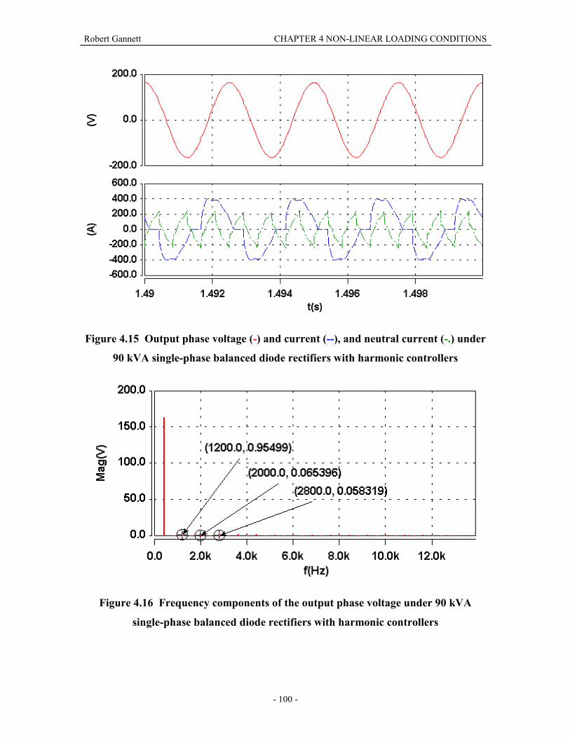
Robert Gannett CHAPTER 4 NON-LINEAR LOADING CONDITIONS
- 100 -
Figure 4.15 Output phase voltage (-) and current (--), and neutral current (-.) under
90 kVA single-phase balanced diode rectifiers with harmonic controllers
Figure 4.16 Frequency components of the output phase voltage under 90 kVA
single-phase balanced diode rectifiers with harmonic controllers

Robert Gannett CHAPTER 4 NON-LINEAR LOADING CONDITIONS
- 101 -
Figure 4.17 displays the abc-coordinate error signal representation in the 5th (a)
and the 7th (b) harmonic frames. The controllers have been turned on under non-linear
loading at a time of 100 milliseconds in order to show the transient response of the
rotating harmonic controllers. It is clear that the DC component of the error signals for
both the 5th and 7th harmonic controllers approaches zero over the span of several 400 Hz
line cycles. The speed of response here is similar to the negative sequence controller for
the unbalance control and the conventional low bandwidth voltage loop control, because
the integrator gains for each of these controllers are the same. The high frequency
components of the error signals represent the harmonic distortion at frequencies other
than the rotating frequency of the harmonic frame.
(a)
(b)
Figure 4.17 (a) 5th harmonic controller transient response for the d-channel;
(b) 7th harmonic controller transient response for the d-channel

Robert Gannett CHAPTER 4 NON-LINEAR LOADING CONDITIONS
- 102 -
4.3.3.3 Stability Analysis
Because the selective harmonic control technique is regulating frequencies at
which the phase has rolled off significantly from the digital delay, it is important that
system stability is investigated. Using the transformation (3.12) from [25], the harmonic
controllers along with the fundamental control can be expressed in the stationary αβ
reference frame. Figure 4.18 displays the magnitude Bode plot for the αβ loop gains.
The large loop gains at the fundamental frequency and the 5th and 7th harmonics ensures
that near zero steady state error tracking of the reference will be achieved for those
frequencies. The phase Bode plot has been omitted here because the large phase jumps at
the resonant frequency of the bandpass filters makes deciphering the phase information
from the Bode plot very difficult. A simpler way to examine the stability of the system is
through the Nyquist stability criterion. According to the Nyquist stability criterion, a
negative unity feedback system is stable if and only if the number of counterclockwise
(CCW) encirclements of the (-1,0) point in the plot of the Nyquist contour mapped
through the loop gain is equal to the number of open loop right half plane (RHP) poles.
Stated in the format of an equation, the Nyquist stability criterion becomes,
pnz NNN += , (4.4)
where zN is the number of closed loop RHP poles, nN is the number of encirclements of
the (-1,0) point (+1 for CW encirclements and –1 for CCW encirclements), and pN is the
number of open loop RHP poles. Obviously, zN must be zero in order for the closed
loop system to be stable. Figure 4.19 displays the Nyquist plot for the αβ loop gains.
Because there are no encirclements of the (-1,0) point and no open loop RHP poles,
initial analysis indicates that the closed loop system is stable.
Figure 4.20 displays the magnitude of the stationary o-channel loop gain for the
harmonic control. The sharp increase in the loop gain at 1200 Hz represents the 3rd
harmonic zero sequence controller. However, the gain at this frequency does not
approach infinity. This is a result of the damping added to the 3rd harmonic bandpass
filter in order to ensure convergence of the simulation package. The phase Bode diagram

Robert Gannett CHAPTER 4 NON-LINEAR LOADING CONDITIONS
- 103 -
is again omitted, in favor of a Nyquist plot to examine system stability. Figure 4.21
shows the Nyquist plot for the o-channel loop gain. For the o-channel, there are no open-
loop RHP poles, and no encirclements of the (-1,0) point, so the initial analysis indicates
closed loop stability.
Figure 4.18 Stationary frame (alpha/beta) loop gain for harmonic control
Figure 4.19 Nyquist diagram of the stationary frame (alpha/beta) loop gain for
harmonic control with modeled digital delay

Robert Gannett CHAPTER 4 NON-LINEAR LOADING CONDITIONS
- 104 -
Figure 4.20 O-channel loop gain for harmonic control
Figure 4.21 Nyquist diagram of the o-channel loop gain for harmonic control with
modeled digital delay
4.3.3.4 Harmonic Control Analysis
The use of harmonic controllers in four-leg VSIs can achieve near zero steady
state errors for the compensated harmonics under non-linear loading. Because the
harmonic currents they draw, and the sequence in which the currents are present, can
characterize non-linear loads, harmonic controllers can be specifically targeted to achieve
zero steady state errors for the dominant voltage harmonics that the non-linear load

Robert Gannett CHAPTER 4 NON-LINEAR LOADING CONDITIONS
- 105 -
creates. As shown above, the use of these harmonic controllers can enable a drastic
improvement in the level of power quality in high power inverter-fed power systems.
The use of harmonic controllers places new constraints on the inverter DC bus
voltage. The harmonic controllers will inject sinusoidal terms into the DC dqo duty
cycles provided by the fundamental controllers. Consequently, the DC voltage overhead
will be reduced, and the DC bus voltage may need to be increased in order to ensure that
the duty cycles do not saturate. This is obviously an important issue that must be
addressed in simulations on a case by case basis, or analyzed further as future work.
It is important also to examine the transient behavior of the harmonic controllers.
Because the bandwidth of the harmonic controllers has been chosen to be quite low, this
control technique will only perform well under slowly time-varying non-linear loading.
Under extreme conditions, such as a fast load step, the harmonic controllers may even
decrease the performance of the inverter. For example, when the harmonic controllers
have reached steady state under a heavy non-linear load, they will be injecting large
sinusoidal terms into the dqo duty cycle to compensate for the voltage distortion. If this
load rapidly steps down to light load, the harmonic controllers will take some time to
reach the new steady state with much smaller sinusoidal duty cycle commands. In the
interim, the large sinusoidal terms in the dqo duty cycles will cause significant output
voltage distortion, because the load is no longer drawing large harmonic currents. The
result is that loads may experience a significant peak voltage transient and repetitive
overvoltage conditions. Therefore, a scheme to reset the harmonic controller integrators
under severe load steps should be employed.
The harmonic control structure detailed above will require a significant amount of
processing time to accomplish. Each rotating frame will require additional
transformations, and thus additional processing time. This fact may limit the number of
harmonics that are possible to control in a physical implementation of the structure
described in the section above. The harmonics that may be regulated are also limited by
another constraint. Assuming that the digital sampling frequency is the same as the
power stage switching frequency, the maximum frequency that can be controlled is half

Robert Gannett CHAPTER 4 NON-LINEAR LOADING CONDITIONS
- 106 -
of the switching frequency, because frequencies above this cannot be resolved by the
specified sampling frequency (Nyquist sampling theorem). Harmonics above half of the
switching frequency cannot be controlled, and thus the output filter must be relied upon
to sufficiently attenuate these harmonics without the possibility of achieving zero steady
state errors.
4.4 Summary of Non-Linear Loading Solutions
Because of the low control bandwidth of high power VSIs, harmonic distortion
due to non-linear loads can be a significant problem in inverter-fed power systems.
Traditional solutions to harmonic distortion in power systems, while effective, all require
additional hardware to be inserted into the power system. The techniques of passive
filtering and paralleling inverters will attenuate the output distortion by lowering the
output impedance of the VSI. However, only the active filter has the possibility to
exactly correct for harmonic distortion and achieve zero steady state errors. The
technique of selective harmonic elimination is unique and extraordinarily beneficial
because it essentially integrates the high power VSI and an active power filter into a
single power stage, made possible through the control structure described in Section
4.3.3. While the utilization of a selective harmonic elimination control scheme will
possibly increase the one-time development time and cost of a high power inverter (due
to more involved DSP coding), it is significantly more profitable than increasing the
recurring manufacturing and parts costs that will accompany the traditional solutions (due
to the additional hardware required). This is the genuine value of the proposed control
strategy.
The proposed control structure is not without its own significant drawbacks. If
several harmonics are to be controlled, then two or more DSPs may be required in order
to accomplish all of the calculations associated with transforming the error signal into all
of the rotating reference frames. This considerably increases the control complexity to
the point that it may become infeasible. However, a simplification of the control scheme
for digital implementation has been proposed in literature [29]. The authors propose an
equivalent control in the stationary frame, consisting of a digital Finite Impulse Response

Robert Gannett CHAPTER 4 NON-LINEAR LOADING CONDITIONS
- 107 -
(FIR) filter of N taps, where N is the number of samples in a fundamental period. In this
manner, compensation for additional harmonics does not require additional calculations,
it only requires a change in the characteristics of the FIR filter. This simplification for
implementation makes the technique of selective harmonic elimination even more
practical and remarkable.

Robert Gannett CHAPTER 5 CONCLUSIONS AND FUTURE RESEARCH
- 108 -
5 CONCLUSIONS AND FUTURE RESEARCH
5.1 Conclusions
The research reported in this thesis has focused on the interesting challenges
presented to inverter-fed, high power systems by specific loading conditions. No-load,
unbalanced loading, and non-linear loading each have unique characteristics that
negatively influence the performance of the VSI. Ideal, infinitely stiff systems are
uninfluenced by loading conditions; however, realistic systems, with finite output
impedances, encounter stability issues, unbalanced phase voltage, and harmonic
distortion. The research reported in this thesis has taken a control approach to solve these
problems.
The traditional solution to lightly loaded or unloaded conditions is simply to
design low controller bandwidths, such that stable operation of the VSI is ensured. While
this approach effectively addresses the problem, the result will be very poor transient
performance of the system. The use of an inner current control loop has been shown,
through theory and simulation, to provide increased damping of the filter poles at light
load, enabling the voltage control bandwidth to be increased. For the system example in
this thesis, the control bandwidth was improved by and order of magnitude, significantly
enhancing transient performance. Utilization of an inner current loop has been shown to
have the added benefit of minimizing the effect of the coupling between the d- and q-
channels in the average plant model.
Traditionally, unbalanced loading conditions are offset in control by using a load
current feedforward controller. While effective in ideal simulations, the load current
feedforward controller’s performance is significantly decreased under realistic
conditions. Therefore, a voltage feedback control structure, based on negative and zero
sequence controllers, has been proposed. As predicted in concept, this control strategy
has been demonstrated through simulation to achieve near zero steady state error for the
inverter under study.

Robert Gannett CHAPTER 5 CONCLUSIONS AND FUTURE RESEARCH
- 109 -
The established solutions for harmonic distortion in power systems, while
effective, all involve the addition of excess hardware. In an attempt to reduce the use of
bulky and expensive hardware, a voltage feedback control scheme has been proposed.
This control structure, in concept, realizes near infinite loop gain at the discrete harmonic
frequencies of interest. The concept has been proven, through simulation of the inverter
under study, to achieve near zero steady state errors for the dominant low frequency
harmonics characteristic of common non-linear loads.
5.2 Direction of Future Research
The research presented in this thesis, while promising for high power VSIs, is
certainly far from complete. Implementation of the control strategies must be
demonstrated in a physical system in order to fully prove the concepts. Experimental
results for the unbalanced and non-linear control techniques on three-leg inverters are
given in literature [24, 29] for low power VSIs (~ 3 kVA). However, application to
higher power four-leg inverters must also be demonstrated.
In order to achieve the best overall inverter performance, all of the proposed
control strategies presented in this thesis should be implemented together. However,
initial simulations including both unbalance and harmonic control resulted in unstable
inverter operation. Further investigation revealed that interaction between the zero
sequence bandpass filters for unbalance control and 3rd harmonic control caused the zero
sequence controller to become unstable. The preliminary solution of simply reducing the
gains of the bandpass filters stabilized the system, but reduced performance. Further
work should be done in order to completely understand the interactions between these
controllers. This will involve a mathematically rigorous study of the steady state and
transient system stability. It is important to note that the stability analyses performed in
this thesis were not mathematically rigorous and only lend an indication of system
stability. Because the stability was analyzed in the stationary reference frame, there is no
single steady state operating point (state variables are time-varying). Thus, this quasi-
steady state analysis only lends insight into the stability at the operating point which the

Robert Gannett CHAPTER 5 CONCLUSIONS AND FUTURE RESEARCH
- 110 -
inverter model is linearized around. As a result, system stability cannot be guaranteed
without further analysis.
All of the concepts and simulation results given in this thesis were the result of a
continuous time domain implementation. In the physical implementation, all of the
control will be realized in a digital signal processor. For this reason, discrete time
domain implementation of the control strategies should tested in simulations in order to
better predict the physical system performance. In addition, a digital model of the VSI
should be developed in order to facilitate more accurate system stability studies. The
simplification for digital implementation of harmonic controllers [29] should also be
studied in more detail for application to four-leg inverters, because this technique holds
some promise for significantly reducing processing times and facilitating the
compensation of additional harmonics.

Robert Gannett APPENDIX A PARK’S TRANSFORMATION
- 111 -
APPENDIX A PARK’S TRANSFORMATION
The time-variation of a balanced three-phase vector representation in orthogonal
abc-coordinates causes it to exist in a two-dimensional subspace that is perpendicular to
the vector [ ]T111 . Based on this fact, a new αβγ -coordinate system is often defined.
The α -axis is defined as the projection of the a-axis in abc-coordinates onto the plane
perpendicular to the vector [ ]T111 . The γ -axis is co-linear with the vector [ ]T111
in abc-coordinates, and the β -axis is defined by the right-hand rule. Thus, the time-
variation of a balanced symmetrical and sinusoidal three-phase vector in abc-coordinates
appears as a vector of constant magnitude rotating counter-clockwise at an angular speed
of ω (fundamental frequency) in αβγ -coordinates. This is represented graphically with
the three-phase variable v in Figure A.1. The γ -axis points out of the paper, and the γ
component of a balanced three-phase vector will always be zero. The γ component will
be nonzero when the three-phase variable is unbalanced or has unequal phase shifts.
Figure A.1 Balanced three-phase vector representation in αβγ -coordinates

Robert Gannett APPENDIX A PARK’S TRANSFORMATION
- 112 -
A rotating coordinate system can now be defined to enable the vector
representation to become a constant without any time-variation. Thus, a dqo-coordinate
system has been defined, such that the d- and q-axes rotate at the angular frequency ω in
the αβ -plane. The o-axis is the same as the γ -axis. This is displayed graphically in
Figure A.2. A balanced three-phase vector representation in this rotating dqo-coordinate
system will now be constant over all time.
Figure A.2 Balanced three-phase vector representation in dqo-coordinates
The transformation matrices to change basis from abc-coordinates to dqo-
coordinates, and from dqo-coordinates to abc-coordinates, without changing the length of
the vectors, are given below in equations (A.1) and (A.2), respectively.
( )
( )
+⋅−
−⋅−⋅−
+⋅
−⋅⋅
=
21
21
21
32sin
32sinsin
32cos
32coscos
32
/πωπωω
πωπωω
ttt
ttt
T dqoabc (A.1)

Robert Gannett APPENDIX A PARK’S TRANSFORMATION
- 113 -
( ) ( )
+⋅−
+⋅
−⋅−
−⋅
⋅−⋅
=
21
32sin
32cos
21
32sin
32cos
21sincos
32
/
πωπω
πωπω
ωω
tt
tt
tt
T abcdqo (A.2)

Robert Gannett APPENDIX B SYMMETRICAL DECOMPOSITION
- 114 -
APPENDIX B SYMMETRICAL DECOMPOSITION
All sinusoidal three-phase variables, balanced or unbalanced, can be decomposed
into balanced positive sequence, negative sequence, and zero sequence components.
Using phasor representation, a balanced three-phase voltage, [ ]Tcba VVV , in
sinusoidal steady state is composed of only positive sequence components,
[ ] [ ]TTcba aaVVVV 21⋅= ++++ , (B.1)
where +V is the positive sequence voltage magnitude and “ a ” is a 120º phase lag,
23
21º120 ⋅−−== − jea j . (B.2)
An unbalanced sinusoidal three-phase voltage will have negative and zero sequence
components, which are given in equations (B.3) and (B.4), respectively,
[ ] [ ]TTcba aaVVVV 21⋅= −−−− , (B.3)
[ ] [ ]TTcba VVVV 1110000 ⋅= , (B.4)
where −V is the negative sequence voltage magnitude and 0V is the zero sequence
voltage magnitude.
It is clear from the definitions above that the positive and negative sequence
components are balanced and can be represented as DC quantities in separate dq
reference frames, rotating in a counter-clockwise (CCW) direction for the positive
sequence and in a clockwise (CW) direction for the negative sequence. The zero
sequence component is the same for all phases, and thus may not be represented as a DC
quantity in a rotating dq reference frame.

Robert Gannett APPENDIX B SYMMETRICAL DECOMPOSITION
- 115 -
The magnitudes for each of the components can be extracted from the three-phase
phasor representation using the transformation matrix given in equation (B.5) below.
Equation (B.6) gives the inverse transformation matrix.
⋅=−+
11111
31 2
2
0/ aaaa
Tabc (B.5)
=−+
11111
2
2/0
aaaaT abc (B.6)

Robert Gannett APPENDIX C LOAD CHARACTERIZATION
- 116 -
APPENDIX C LOAD CHARACTERIZATION
This appendix will characterize two common types of non-linear power system
loads according to the harmonic currents that they draw from balanced three-phase
sources. The currents can be represented as a summation of harmonic components using
a trigonometric Fourier series expansion:
( ) ∞
=
∞
=
++=1
01
00 sincosn
nn
n tnbtnaatx ωω , (C.1)
with the following definitions,
( )=0
1
00 T
dttxT
a , (C.2)
( )=0
cos20
0Tn dttntx
Ta ω , (C.3)
( )=0
sin20
0Tn dttntx
Tb ω . (C.4)
C.1 Three-Phase Diode Rectifier
A single period of the phase currents drawn by a three-phase diode rectifier takes
the form of those shown in Figure C.1. The currents drawn by the rectifier may by
moderately different due to varying rectifier filters and loads; however, the currents will
always take a similar form. Equations (C.5) to (C.7) give the discontinuous time domain
functions for the phase currents shown in Figure C.1. In these equations, oT is the period
of the fundamental frequency, and “A” is the amplitude of the current peaks.

Robert Gannett APPENDIX C LOAD CHARACTERIZATION
- 117 -
Figure C.1 Phase a (-), phase b (--), and phase c (-.) currents for a three-phase diode
rectifier
≤≤≤≤−
≤≤≤≤≤≤−
≤≤
=
065
0
65
32
0
32
2
230
360
6
0
00
00
00
00
0
),3sin( ),3sin(
,0 ),3sin( ),3sin(
0 ,0
)(
TttAttA
tttAttA
t
ti
T
TT
TT
TT
TT
T
a
ωω
ωω
(C.5)
≤≤≤≤≤≤−
≤≤≤≤≤≤−
=
065
65
32
0
32
20
23
360
60
0
00
00
00
00
0
,0 ),3sin(
),3sin( ,0
),3sin(0 ),3sin(
)(
TtttAttA
tttAttA
ti
T
TT
TT
TT
TT
T
b
ωω
ωω
(C.6)
≤≤−≤≤
≤≤≤≤−
≤≤≤≤
=
065
0
65
32
32
20
230
36
60
0
00
00
00
00
0
),3sin( ,0
),3sin( ),3sin(
,00 ),3sin(
)(
TttAt
ttAttA
tttA
ti
T
TT
TT
TT
TT
T
c
ω
ωω
ω
(C.7)

Robert Gannett APPENDIX C LOAD CHARACTERIZATION
- 118 -
Using these definitions for the phase currents, the trigonometric Fourier series
coefficients for each of the phases can be calculated. It is clear that the 0a coefficient is
zero for each of the phase currents, because the average value of all of the waveforms
will be zero. The na coefficients for each phase are calculated to be:
( )( ) ( ) ( )( ) ( )
( )( ) ( ) ( )( ) ( )
( )( ) ( )( ) ( )( ) ( )( ) ( )( )
( )( ) ( )( ) ( )( ) ( )( ) ( )( )
−−−−+−−−−−+−+
++−+++−+−++−⋅=
+−+
+−⋅=
)3(3cos3cos23cos3cos3cos21
)3(3cos3cos23cos3cos3cos21
2
cos3sincos3sin
cos3sincos3sin2
35
34
32
3
35
34
32
3
0000
000
000
605
302
302
20
30
60
60
nnnnnn
nnnnnnA
dttntAdttntA
dttntAdttntAT
a
T
T
T
T
T
T
T
na
ππππ
ππππ
π
ππ
ωωωω
ωωωω
,
(C.8)
( )( ) ( ) ( )( ) ( )
( )( ) ( ) ( )( ) ( )
( )( ) ( )( ) ( )( ) ( )( ) ( )( )
( )( ) ( )( ) ( )( ) ( )( ) ( )( )
−−−−+−−−−−+−+
++−+++−+−++−⋅=
+−+
+−⋅=
)3(3cos3cos23cos3cos3cos21
)3(3cos3cos23cos3cos3cos21
2
cos3sincos3sin
cos3sincos3sin2
35
34
32
3
35
34
32
3
0000
000
000
605
302
302
20
30
60
60
nnnnnn
nnnnnnA
dttntAdttntA
dttntAdttntAT
a
T
T
T
T
T
T
T
nb
ππππ
ππππ
π
ππ
ωωωω
ωωωω
,
(C.9)
( )( ) ( ) ( )( ) ( )
( )( ) ( ) ( )( ) ( )
( )( ) ( )( ) ( )( ) ( )( ) ( )( ) ( )( )
( )( ) ( )( ) ( )( ) ( )( ) ( )( ) ( )( )
−−+−−−−−+−−−−+
++++−+−+++−+−⋅=
−++
−+⋅=
)3(32cos3cos3cos3cos23cos3cos1
)3(32cos3cos3cos3cos23cos3cos1
2
cos3sincos3sin
cos3sincos3sin2
35
34
32
3
35
34
32
3
0000
000
000
0
605
302
20
20
30
60
nnnnnnn
nnnnnnnA
dttntAdttntA
dttntAdttntAT
a
T
nc
T
T
T
T
T
T
ππ
πππ
ωωωω
ωωωω
ππππ
ππππ
.
(C.10)
The nb coefficient for phase c is zero by inspection because the c phase current
representation is symmetric about the y-axis (even function). The nb coefficients for the
other phases are calculated to be:

Robert Gannett APPENDIX C LOAD CHARACTERIZATION
- 119 -
( )( ) ( ) ( )( ) ( )
( )( ) ( ) ( )( ) ( )
( )( ) ( )( ) ( )( ) ( )( ) ( )( ) ( )( )
( )( ) ( )( ) ( )( ) ( )( ) ( )( ) ( )( )
++−+++−+−+++−+
−−+−−−+−+−−−=
+−+
+−⋅=
)3(32sin3sin23sin3sin3sin23sin
)3(32sin3sin23sin3sin3sin23sin
2
sin3sinsin3sin
sin3sinsin3sin2
35
34
32
3
35
34
32
3
0000
00000
0
605
605
302
20
30
30
60
nnnnnnn
nnnnnnnA
dttntAdttntA
dttntAdttntAT
b
T
na
T
T
T
T
T
T
T
ππ
πππ
ωωωω
ωωωω
ππππ
ππππ
,
(C.11)
( )( ) ( ) ( )( ) ( )
( )( ) ( ) ( )( ) ( )
( )( ) ( )( ) ( )( ) ( )( ) ( )( )
( )( ) ( )( ) ( )( ) ( )( ) ( )( )
++−+++−+−++
−−+−−−+−+−−⋅=
+−+
+−⋅=
)3(3sin3sin23sin3sin3sin2
)3(3sin3sin23sin3sin3sin2
2
sin3sinsin3sin
sin3sinsin3sin2
35
34
32
3
35
34
32
3
0000
000
000
605
302
302
20
30
60
60
nnnnnn
nnnnnnA
dttntAdttntA
dttntAdttntAT
b
T
T
T
T
T
T
T
nb
ππππ
ππππ
π
ππ
ωωωω
ωωωω
.
(C.12)
Normalizing these coefficients (A=1) and examining the 5th harmonic (n=5)
yields the following equations for the 5th harmonic component of the phase currents:
( ) tttia 005 5sin3101.05cos179.0 ωω += , (C.13)
( ) tttib 005 5sin3101.05cos179.0 ωω −= , (C.14)
( ) ttic 05 5cos3581.0 ω−= . (C.15)
Rearranging equations (C.13) to (C.15) yields,
( ) ( )º305sin3581.0 05 += ttia ω , (C.16)
( ) ( )º1505sin3581.0 05 += ttib ω , (C.17)
( ) ( )º905sin3581.0 05 −= ttic ω . (C.18)
From equations (C.16) to (C.18), it is clear that phase a leads phase c by 120º and lags
phase b by 120º. Thus, the phase sequence is phase a →phase c →phase b. This
Robert Gannett APPENDIX C LOAD CHARACTERIZATION
- 120 -
obviously represents the negative sequence, and would thus rotate in the negative, or CW,
direction in the αβ -plane.
Examining the 7th harmonic (n=7) yields the following 7th harmonic phase current
equations:
( ) tttia 007 7sin124.07cos0716.0 ωω −= , (C.19)
( ) tttib 007 7sin124.07cos0716.0 ωω += , (C.20)
( ) ttic 07 7cos1432.0 ω−= . (C.21)
Rearranging equations (C.19) to (C.21) yields,
( ) ( )º1507sin1432.0 07 += ttia ω , (C.22)
( ) ( )º307sin1432.0 07 += ttib ω , (C.23)
( ) ( )º907sin1432.0 07 −= ttic ω . (C.24)
From equations (C.22) to (C.24), it is clear that phase a leads phase b by 120º and lags
phase c by 120º. Thus, the phase sequence is phase a →phase b →phase c.
Consequently, the 7th harmonic components of the phase currents exist in the positive
sequence, and rotate in the CCW direction in the αβ -plane.
Further analysis of the Fourier series representations of the phase currents reveals
that all of the even harmonics and odd triplen harmonics (3rd,9th,15th, etc.) are identically
zero. Additionally, all of the ( )[ ]16 −⋅ m harmonics, as demonstrated for the 5th
harmonic, will be negative sequence, and all of the ( )[ ]16 +⋅ m harmonics, as
demonstrated for the 7th harmonic, will exist in the positive sequence (where m is any
positive, real integer).

Robert Gannett APPENDIX C LOAD CHARACTERIZATION
- 121 -
C.2 Single-Phase Diode Rectifier
For the purpose of this discussion, the single-phase diode rectifier displayed in
Figure 4.4 will be used. Although other single-phase diode rectifier topologies exist, this
topology along with a four diode bridge rectifier are the most common and will display
similar harmonic results. Figure C.2 displays a single period of the phase currents
(neutral current omitted) drawn by a typical load of balanced single-phase diode
rectifiers. Equations (C.25) to (C.27) give the discontinuous time domain functions for
the phase currents shown in Figure C.2. In these equations, oT is the period of the
fundamental frequency, and “A” is the amplitude of each of the current peaks.
Figure C.2 Phase a (-), phase b (--), and phase c (-.) currents for a load of single-
phase diode rectifiers

Robert Gannett APPENDIX C LOAD CHARACTERIZATION
- 122 -
( )
( )
≤≤≤≤
≤≤≤≤
=
oT
o
TT
TTo
T
a
TttwAt
ttwAt
ti
32
32
2
26
6
0
00
00
0
,sin,0
,sin0,0
)( (C.25)
( )( )
≤≤≤≤−
≤≤≤≤−
=
oT
TTo
TT
To
b
TtttwA
tttwA
ti
65
65
2
23
3
0
00
00
0
,0,3
2sin,0
0,32sin
)( π
π
(C.26)
( )( )( )
≤≤+≤≤
≤≤+≤≤
≤≤+
=
oT
o
TT
TTo
TT
To
c
TttwAt
ttwAt
ttwA
ti
65
65
32
32
3
36
6
0
00
00
00
0
,32sin
,0,3
2sin,0
0,32sin
)(
π
π
π
(C.27)
Using equations (C.25) to (C.27), the trigonometric Fourier series coefficients for
each of the phases can be calculated. The 0a coefficient is zero for each of the phase
currents, because the average value of all of the waveforms is clearly zero. The na
coefficients for each phase are calculated to be:
( ) ( )
( )( ) ( )( ) ( )( ) ( )( )
( )( ) ( )( ) ( )( ) ( )( )
−−−−+−−−+
++−+++−+⋅=
+⋅=
)1(12cos1cos1cos1cos
)1(12cos1cos1cos1cos
2
cos)sin(cos)sin(2
34
3
34
3
32
0
2
6
00
nnnnn
nnnnnA
dttntdttntAT
ao
o
o
o
T
To
T
Tona
ππ
πππ
ωωωω
ππ
ππ
, (C.28)
( ) ( )
( ) ( )( ) ( )( ) ( )( )
( ) ( )( ) ( )( ) ( )( )
−−−−−−+−−−−+
+−+−−++−+−−⋅=
−+−⋅=
)1(1cos1cos1coscos
)1(1cos1cos1coscos
2
cos)sin(cos)sin(2
32
35
32
32
32
32
32
35
32
32
32
32
65
2
032
3
003
2
0
nnnn
nnnnA
dttntdttntAT
ao
o
o T
To
T
onb
ππππππ
ππππππ
ππ
π
ππ
ωωωω, (C.29)

Robert Gannett APPENDIX C LOAD CHARACTERIZATION
- 123 -
( ) ( ) ( )
( ) ( )( ) ( )( ) ( )( ) ( )( ) ( )( )
( ) ( )( ) ( )( ) ( )( ) ( )( ) ( )( )
−+−−+−++−−+−++−−+
+++−+++++−+++++−⋅=
+++++⋅=
)1(12cos1cos1cos1cos1coscos
)1(12cos1cos1cos1cos1coscos
2
cos)sin(cos)sin(cos)sin(2
32
32
35
32
34
32
32
32
332
32
32
35
32
34
32
32
32
332
65
032
32
3
032
6
003
2
0
nnnnnn
nnnnnnA
dttntdttntdttntAT
ao
o
o
o
o T
To
T
To
T
onc
ππππππππππ
ππππππππππ
πππ
π
ππ
ωωωωωω. (C.30)
The nb coefficients for each of the phases are calculated to be:
( ) ( )
( )( ) ( )( ) ( )( ) ( )( )
( )( ) ( )( ) ( )( ) ( )( )
++−+++−++
−−+−−−+−−⋅=
+⋅=
)1(12sin1sin1sin1sin
)1(12sin1sin1sin1sin
2
sin)sin(sin)sin(2
34
3
34
3
32
0
2
6
00
nnnnn
nnnnnA
dttntdttntAT
bo
o
o
o
T
To
T
Tona
ππ
πππ
ωωωω
ππ
ππ
, (C.31)
( ) ( )
( ) ( )( ) ( )( ) ( )( )
( ) ( )( ) ( )( ) ( )( )
+−+−−++−+−−+
−−−+−−−−−+−−⋅=
−+−⋅=
)1(1sin1sin1sinsin
)1(1sin1sin1sinsin
2
sin)sin(sin)sin(2
32
35
32
32
32
32
32
35
32
32
32
32
65
2
032
3
003
2
0
nnnn
nnnnA
dttntdttntAT
bo
o
o T
To
T
onb
ππππππ
ππππππ
ππ
π
ππ
ωωωω, (C.32)
( ) ( ) ( )
( ) ( )( ) ( )( ) ( )( ) ( )( ) ( )( )
( ) ( )( ) ( )( ) ( )( ) ( )( ) ( )( )
+++−+++++−+++++−+
−+−++−−+−++−−+−+−⋅=
+++++⋅=
)1(12sin1sin1sin1sin1sinsin
)1(12sin1sin1sin1sin1sinsin
2
sin)sin(sin)sin(sin)sin(2
32
32
35
32
34
32
32
32
332
32
32
35
32
34
32
32
32
332
65
032
32
3
032
6
003
2
0
nnnnnn
nnnnnnA
dttntdttntdttntAT
bo
o
o
o
o T
To
T
To
T
onc
ππππππππππ
ππππππππππ
πππ
π
ππ
ωωωωωω . (C.33)
Normalizing these coefficients (A=1) and examining the 3rd harmonic (n=3)
yields the following equations for the 3rd harmonic component of the phase currents:
( ) ( ) ( )ttti ooa ωω 3sin2067.03cos1194.03 −= , (C.34)
( ) ( ) ( )ttti oob ωω 3sin2067.03cos1194.03 −= , (C.35)
( ) ( ) ( )ttti ooc ωω 3sin2067.03cos1194.03 −= . (C.36)
The 3rd harmonic components of the phase currents are all identical, and thus the 3rd
harmonic currents clearly exist in the zero sequence.

Robert Gannett APPENDIX C LOAD CHARACTERIZATION
- 124 -
Examining the 5th harmonic (n=5) yields the following 5th harmonic phase current
equations:
( ) tttia 005 5sin0689.05cos1194.0 ωω += , (C.37)
( ) ttib 05 5sin1378.0 ω−= , (C.38)
( ) ttti oc ωω 5sin0689.05cos1194.0 05 +−= . (C.39)
Rearranging equations (C.37) to (C.39) yields,
( ) ( )º605sin1378.0 05 += ttia ω , (C.40)
( ) ( )º1805sin1378.0 05 += ttib ω , (C.41)
( ) ( )º605sin1378.0 05 −= ttic ω . (C.42)
From equations (C.40) to (C.42), it is clear that phase a leads phase c by 120º and lags
phase b by 120º. As did the 5th harmonic for the three-phase diode rectifier, the phase
sequence here is phase a →phase c →phase b. This obviously represents the negative
sequence, and would thus rotate in the negative, or CW, direction in the αβ -plane.
Examining the 7th harmonic (n=7) yields the following 7th harmonic phase current
equations:
( ) tttia 007 7sin0345.07cos0597.0 ωω +−= , (C.43)
( ) ttib 07 7sin0689.0 ω−= , (C.44)
( ) ttti oc 07 7cos0345.07cos0597.0 ωω += . (C.45)
Rearranging equations (C.43) to (C.45) yields,
( ) ( )º607sin0689.0 07 −= ttia ω , (C.46)

Robert Gannett APPENDIX C LOAD CHARACTERIZATION
- 125 -
( ) ( )º1807sin0689.0 07 −= ttib ω , (C.47)
( ) ( )º607sin0689.0 07 += ttic ω . (C.48)
From equations (C.46) to (C.48), it is clear that phase a leads phase b by 120º and lags
phase c by 120º. As was true for the 7th harmonic for three-phase diode rectifiers, the
phase sequence here is phase a →phase b →phase c. Consequently, the 7th harmonic
components of the phase currents exist in the positive sequence, and rotate in the CCW
direction in the αβ -plane.
By further examination of the Fourier series coefficients, it can be determined that
all of the even harmonic components of the phase currents will be exactly zero. Also, all
of the additional odd triplen harmonics, like the 3rd harmonic, will exist in the zero
sequence. Finally, as was determined for the three-phase diode rectifiers, all of the
( )[ ]16 −⋅ m harmonics will be negative sequence, and all of the ( )[ ]16 +⋅ m harmonics
will exist in the positive sequence (where m is any positive, real integer).

Robert Gannett REFERENCES
- 126 -
REFERENCES
[1] J. Platt and J. St. Aubyn, Uninterruptible Power Supplies, Peter Peregrinus Ltd., 1992.
[2] D. C. Griffith, Uninterruptible Power Supplies – Power Conditioners for Critical Equipment, Marcel Dekker, Inc., 1989.
[3] U. B. Jensen, “A New Control Method for 400-Hz Ground Power Units for Aircraft,” IEEE Transactions on Industry Applications, vol.36, no.1, January - February 2000, pp.180-187.
[4] F. Schettler, H. Huang, and N. Christl, “HVDC Transmission Systems Using Voltage Sourced Converters - Design and Applications,” Proceedings of the 2000 IEEE Power Engineering Society Summer Meeting, vol. 2, pp. 715-720.
[5] W. Sweet, “Networking Assets – Distributed Generation,” IEEE Spectrum, vol. 38, no.1, January 2001, pp. 84-88.
[6] IEEE 241, “IEEE Recommended Practice for Electric Power Systems in Commercial Buildings,” 1983.
[7] ANSI/IEEE 242, “IEEE Recommended Practice for Protection and Coordination of Industrial and Commercial Power Systems,” 1986.
[8] NEMA MG1, “Motors and Generators,” 1978.
[9] IEEE 519, “IEEE Guide for Harmonic Control and Reactive Compensation of Static Power Converters,” 1981.
[10] IEEE 446, “IEEE Recommended Practice for Emergency and Standby Power Systems for Industrial and Commercial Applications,” 1987.
[11] MIL-STD-704E, “Aircraft Electric Power Characteristics,” 1991.
[12] T. Gilmore and R. G. Sladky, “Ratings of Semiconductors for AC Drives,” IEEE Transactions on Industry Applications, vol. 37, no.2, March/April 2001, pp. 434-441.
[13] J. E. Marshall, Control of Time-Delay Systems, IEE, 1979.
[14] S. Hiti and D. Boroyevich, “Small-Signal Modeling of Three-Phase PWM Modulators,” Proceedings of the 1996 IEEE Power Electronics Specialists Conference, vol. 1, pp. 550-555.
[15] E. H. J. Pallett, Aircraft Electric Systems, 2nd ed., Pitman Publishing Ltd., 1979.

Robert Gannett REFERENCES
- 127 -
[16] R. Zhang, “High Performance Power Converter Systems for Nonlinear and Unbalanced Load/Source,” Dissertation, Virginia Tech, 1998.
[17] N. H. Kutkut and G. Luckjiff, “Current Mode Control of a Full Bridge DC-to-DC Converter with a Two Inductor Rectifier,” Proceedings of the 1997 IEEE Power Electronics Specialists Conference, vol. 1, pp. 203-209.
[18] L. Dixon, “Average Current Mode Control of Switching Power Supplies,” Unitrode Application Note U-140, 1999.
[19] N. S. Nise, Control Systems Engineering, 2nd Ed., Addison-Wesley Publishing Co., 1995.
[20] M. J. Ryan, W. E. Brumsickle, and R. D. Lorenz, “Control Topology Options for Single-Phase UPS Inverters,” IEEE Transactions on Industry Applications, vol. 33, no. 2, March/April 1997, pp.493-501.
[21] J. S. Bay, Fundamentals of Linear State Space Systems, WCB/McGraw-Hill, 1999.
[22] M. J. Ryan and R. D. Lorenz, “A High Performance Sine Wave Inverter Controller with Capacitor Current Feedback and “Back-EMF” Decoupling,” Proceedings of the 1995 IEEE Power Electronics Specialists Conference, vol. 1, pp. 507-513.
[23] M. J. Ryan, R. W. De Doncker, and R. D. Lorenz, “Decoupled Control of a 4-Leg Inverter via a New 4x4 Transformation Matrix,” Proceedings of the 1999 IEEE Power Electronics Specialists Conference, vol. 1, pp. 187-192.
[24] P. Hsu and M. Behnke, “A Three-Phase Synchronous Frame Controller for Unbalanced Load,” Proceedings of the 1998 IEEE Power Electronics Specialists Conference, vol. 2, pp. 1369-1374.
[25] D. N. Zmood and D. G. Holmes, “Stationary Frame Current Regulation of PWM Inverters with Zero Steady State Error,” Proceedings of the 1999 IEEE Power Electronics Specialists Conference, vol. 2, pp. 1185-1190.
[26] W. M. Grady, M. J. Samotyj, and A. H. Noyola, “Survey of Active Power Line Conditioning Methodologies,” IEEE Transactions on Power Delivery, vol. 5, no. 3, July 1990, pp. 1536-1542.
[27] T. Kawabata and S. Higashino, “Parallel Operation of Voltage Source Inverters,” IEEE Transactions on Industry Applications, vol. 24, no. 2, March/April 1988, pp. 281-287.
[28] Z. Ye, D. Boroyevich, and F. C. Lee, “Modeling and Control of Zero-Sequence Current in Parallel Multi-Phase Converters,” Proceedings of the 2000 IEEE Power Electronics Specialists Conference, vol. 2, pp. 680-685.

Robert Gannett REFERENCES
- 128 -
[29] P. Mattavelli and S. Fasolo, “Implementation of Synchronous Frame Harmonic Control for High-Performance AC Power Supplies,” Proceedings of the 2000 IEEE Industry Applications Conference, vol. 3, pp. 1988-1995.

Robert Gannett VITA
- 129 -
VITA
Robert Ashley Gannett was born in Madison, Wisconsin on November 23, 1978.
He entered Virginia Polytechnic Institute and State University in August of 1996 in the
engineering curriculum.
During the summers of 1998 and 1999, the author worked as an engineering
intern at Lutron Electronics in Coopersburg, Pennsylvania. While employed by Lutron,
he tested lighting systems, redesigned a low-power AC/DC power supply, and wrote
algorithms for embedded processors.
In the fall of 1999, he enrolled into the 5-year B.S./M.S. program at Virginia
Polytechnic Institute and State University. In September of 1999, he began working as
an undergraduate at the Center for Power Electronics Systems. He received his B.S.
degree in Electrical Engineering in May of 2000 from Virginia Polytechnic Institute and
State University. The author will begin full-time employment with Lockheed-Martin
upon completion of his M.S. degree.
The author is a member of the Sigma Phi Epsilon Fraternity, and the Eta Kappa
Nu and Golden Key Honor Societies. His research interests include three-phase, high
power inverters and modeling and control of power electronics circuits.