control design of a single-phase dc/ac inverter for pv
TRANSCRIPT
University of Arkansas, FayettevilleScholarWorks@UARK
Theses and Dissertations
5-2016
Control Design of a Single-Phase DC/AC Inverterfor PV ApplicationsHaoyan LiuUniversity of Arkansas, Fayetteville
Follow this and additional works at: http://scholarworks.uark.edu/etd
Part of the Controls and Control Theory Commons, and the Power and Energy Commons
This Thesis is brought to you for free and open access by ScholarWorks@UARK. It has been accepted for inclusion in Theses and Dissertations by anauthorized administrator of ScholarWorks@UARK. For more information, please contact [email protected], [email protected].
Recommended CitationLiu, Haoyan, "Control Design of a Single-Phase DC/AC Inverter for PV Applications" (2016). Theses and Dissertations. 1618.http://scholarworks.uark.edu/etd/1618

Control Design of a Single-Phase DC/AC Inverter for PV Applications
A thesis submitted in partial fulfillment of the requirements for the degree of
Master of Science in Electrical Engineering
by
Haoyan Liu Harbin University of Science and Technology Bachelor of Engineering in Automation, 2012
May 2016 University of Arkansas
This thesis is approved for recommendation to the Graduate Council. ____________________________________ Dr. Alan Mantooth Thesis Director ____________________________________ ____________________________________ Dr. Simon Ang Dr. Roy McCann Committee Member Committee Member

Abstract
This thesis presents controller designs of a 2 kVA single-phase inverter for photovoltaic
(PV) applications. The demand for better controller designs is constantly rising as the renewable
energy market continues to rapidly grow. Some background research has been done on solar
energy, PV inverter configurations, inverter control design, and hardware component selection.
Controllers are designed both for stand-alone and grid-connected modes of operation. For stand-
alone inverter control, the outer control loop regulates the filter capacitor voltage. Combining the
synchronous frame outer control loop with the capacitor current feedback inner control loop, the
system can achieve both zero steady-state error and better step load performance. For grid-tied
inverter control, proportional capacitor current feedback is used. This achieves the active
damping needed to suppress the LCL filter resonance problem. The outer loop regulates the
inverter output current flowing into the grid with a proportional resonant controller and harmonic
compensators. With a revised grid synchronization unit, the active power and reactive power can
be decoupled and controlled separately through a serial communication based user interface. To
validate the designed controllers, a scaled down prototype is constructed and tested with a digital
signal processor (DSP) TMS320F28335.

○C 2016 by Haoyan Liu All Rights Reserved

Acknowledgements
I am very fortunate to have performed my master’s level graduate study at the University
of Arkansas, where I met erudite professors and collaborative colleagues. I would like to give my
special thanks to my academic advisor, Prof. Alan Mantooth, who inspires me to achieve my
academic goals with his experience, professional ethics, and leadership. Without his guidance
and mentorship, I could not have completed my graduation requirements. I am also very grateful
for the opportunities and diverse work environment he has created for us.
Thanks are also due to my thesis committee members, Dr. Roy McCann and Dr. Simon
Ang, for their technical assistance and patient support throughout my graduate study.
It has been a great honor to have met Yuzhi Zhang and Yusi Liu from Dr. Mantooth’s
power electronics laboratory, who have shared great academic experience with me. Their
contributions are extremely valuable to the progress I have made throughout my research study. I
also appreciate the help from my other colleagues: Janviere Umuhoza, Joe Moquin, Tavis
Clemmer, Shuang Zhao, and Fahad Hossain. I would like to thank Chris Farnell for sharing his
knowledge and experience as well as keeping the laboratory well managed and organized.

Table of Contents
Chapter 1 Introduction and Theoretical Background ................................................................ 1
1.1 Introduction and Motivation............................................................................................. 1
1.2 Theoretical Background ................................................................................................... 3
1.2.1 Solar Energy ..................................................................................................................... 3
1.2.2 Solar System Configurations ............................................................................................ 6
1.2.2.1 Single-Stage Centralized Inverter ......................................................................... 6
1.2.2.2 Single-Stage String Inverter .................................................................................. 7
1.2.2.3 Two-Stage String Inverter ..................................................................................... 7
1.2.2.4 Two-Stage Centralized Inverter ............................................................................ 8
1.2.3 DC/AC Inverter Topologies ............................................................................................. 9
1.2.4 Inverter Filter Topologies................................................................................................. 9
1.2.5 LCL Filter Design Considerations ................................................................................. 12
1.2.6 Active Damping ............................................................................................................. 16
1.2.6.1 Notch Filter ......................................................................................................... 16
1.2.6.2 Virtual Resistance ............................................................................................... 17
1.3 Hardware Component Sizing ......................................................................................... 19
Chapter 2 Controller Design of Stand-Alone Inverter ............................................................. 22
2.1 Inner Current Loop Design ............................................................................................ 22
2.2 Outer Current Loop Design ............................................................................................ 25
2.3 DQ Frame Control .......................................................................................................... 27
2.4 Proportional Resonant Control ....................................................................................... 31
2.5 Summary ........................................................................................................................ 36

Chapter 3 Controller Design of Grid-Tied Inverter ................................................................. 38
3.1 Current Controller Design .............................................................................................. 39
3.2 Phase Locked Loop and Amplitude Detection ............................................................... 43
3.3 Active and Reactive Power Flow Control ...................................................................... 52
3.4 Simulation Results.......................................................................................................... 54
3.5 Summary ........................................................................................................................ 61
Chapter 4 Experimental Test Results ...................................................................................... 62
4.1 Experimental Test Station .............................................................................................. 62
4.1.1 Stand-Alone Mode ......................................................................................................... 63
4.1.2 Grid-Tied Mode.............................................................................................................. 67
Chapter 5 Conclusion and Future Work .................................................................................. 73
5.1 Conclusion ...................................................................................................................... 73
5.2 Future Work ................................................................................................................... 74
References ..................................................................................................................................... 75

Figures
Fig. 1-1: U.S. market renewable energy usage [3] ......................................................................... 1
Fig. 1-2: Equivalent circuit of a solar cell....................................................................................... 3
Fig. 1-3: I-V curves of a PV string (constant temperature) ............................................................ 4
Fig. 1-4: P-V curves of a PV string (constant temperature) ........................................................... 4
Fig. 1-5: I-V curves of a PV string (constant irradiance) ............................................................... 5
Fig. 1-6: P-V curves of a PV string (constant irradiance) ............................................................... 5
Fig. 1-7: Single-stage centralized inverter ...................................................................................... 6
Fig. 1-8: Single-stage string inverter .............................................................................................. 7
Fig. 1-9: Two-stage string inverter ................................................................................................. 8
Fig. 1-10: Two-stage centralized inverter ....................................................................................... 8
Fig. 1-11: Single-phase H-bridge inverter topology ....................................................................... 9
Fig. 1-12: L type filter ................................................................................................................... 10
Fig. 1-13: LC type filter ................................................................................................................ 10
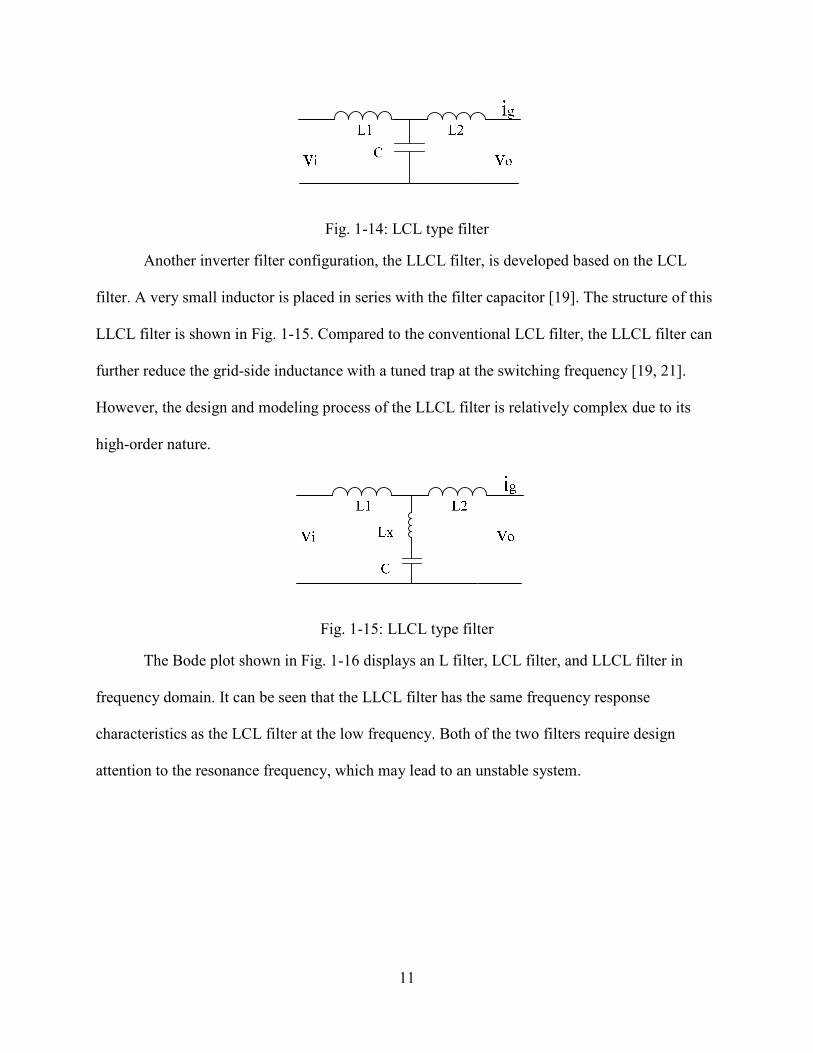
Fig. 1-14: LCL type filter.............................................................................................................. 11
Fig. 1-15: LLCL type filter ........................................................................................................... 11
Fig. 1-16: Bode plot of different filter types ................................................................................. 12
Fig. 1-17: PV inverter leakage current with unipolar switching ................................................... 14
Fig. 1-18: PV inverter leakage current with bipolar switching ..................................................... 14
Fig. 1-19: LCL filter passive damping resistance placement ....................................................... 15
Fig. 1-20: LCL filter with passive damping resistance ................................................................. 15
Fig. 1-21: Active damping technique with a notch filter .............................................................. 16
Fig. 1-22: LCL filter active damping with a notch filter .............................................................. 17

Fig. 1-23: Active damping with the grid injected current and filter capacitor current ................. 18
Fig. 1-24: Equivalent circuit with filter capacitor current feedback ............................................. 18
Fig. 1-25: Active damping with the grid injected current only..................................................... 18
Fig. 1-26: Equivalent circuit with high pass filtered grid current feedback ................................. 18
Fig. 2-1: Island mode inverter circuit diagram ............................................................................. 22
Fig. 2-2: Inner control system diagram using inverter-side inductor current i�� feedback .......... 23
Fig. 2-3: Inner control system diagram using capacitor current i� feedback ................................ 23
Fig. 2-4: Bode plots of the uncompensated and compensated inner loop .................................... 24
Fig. 2-5: Step response of the compensated inner control loop .................................................... 25
Fig. 2-6: Outer loop control diagram ............................................................................................ 25
Fig. 2-7: Bode plots of the uncompensated and compensated outer voltage loop ........................ 26
Fig. 2-8: Step response of the compensated outer voltage loop ................................................... 27
Fig. 2-9: Dual-PI controlled inverter voltage tracking error ......................................................... 27
Fig. 2-10: A DQ based control diagram of single-phase inverters ............................................... 28
Fig. 2-11: Comparison of control performance between the two inner feedback methods .......... 29
Fig. 2-12: Inverter output voltage ................................................................................................. 29
Fig. 2-13: Inverter output current.................................................................................................. 30
Fig. 2-14: Voltage tracking error comparison between PI control and DQ frame control ........... 30
Fig. 2-15: Inverter output with 1.4 kVar inductive load and 1.4 kW resistive load ..................... 31
Fig. 2-16: Inverter output with 1.4 kVar capacitive load and 1.4 kW resistive load .................... 31
Fig. 2-17: Bode plot of PR controllers with a fixed proportional gain term ................................. 32
Fig. 2-18: Bode plot of PR controllers with a fixed integral gain term ........................................ 33
Fig. 2-19: Bode plot of nonideal PR controllers with a fixed proportional gain term .................. 33

Fig. 2-20: Bode plot of nonideal PR controllers with a fixed integral gain term ......................... 34
Fig. 2-21: Bode plots of the uncompensated and nonideal PR compensated outer voltage loop . 35
Fig. 2-22: Step response of the compensated outer voltage loop with nonideal PR control ........ 35
Fig. 2-23: Closed-loop Bode plot of the dual-loop system with nonideal PR control .................. 36
Fig. 2-24: Voltage tracking error comparison between PI control and nonideal PR control ........ 36
Fig. 3-1: Grid-tied inverter circuit diagram .................................................................................. 38
Fig. 3-2: Grid-tied inverter control block diagram ....................................................................... 39
Fig. 3-3: Inner loop controller selection ....................................................................................... 40
Fig. 3-4: Bode plots of the compensated and uncompensated systems ........................................ 40
Fig. 3-5: Bode plots of the compensated systems with various K�� ............................................. 41
Fig. 3-6: Bode plots of the compensated systems with various K�� ............................................. 42
Fig. 3-7: Bode plots of the compensated systems with various L ............................................... 42
Fig. 3-8: Step response of the dual-loop control system ............................................................... 43
Fig. 3-9: Sinusoidal signal tracking response of the designed system .......................................... 43
Fig. 3-10: Zero-crossing detection based PLL .............................................................................. 44
Fig. 3-11: Basic phase error detection based PLL ........................................................................ 44
Fig. 3-12: OSG based single-phase PLL....................................................................................... 45
Fig. 3-13: Bode plot of H�(s) ....................................................................................................... 46
Fig. 3-14: Bode plot of H�(s) ....................................................................................................... 47
Fig. 3-15: Second order generalized integrator for the OSG unit [12] ......................................... 48
Fig. 3-16: Revised SOGI for the OSG unit ................................................................................... 48
Fig. 3-17: Bode plot of H�'(s) ...................................................................................................... 49
Fig. 3-18: Peak detection based grid synchronization .................................................................. 50

Fig. 3-19: Revised SOGI performance under frequency drift ...................................................... 50
Fig. 3-20: Revised SOGI performance under voltage sag ............................................................ 51
Fig. 3-21: Revised SOGI performance under harmonics and DC offset polluted grid ................. 52
Fig. 3-22: PI based active power control loop .............................................................................. 53
Fig. 3-23: PI based reactive power control loop ........................................................................... 53
Fig. 3-24: Active and reactive power controller ........................................................................... 53
Fig. 3-25: Inverter output current.................................................................................................. 55
Fig. 3-26: Steady-state tracking error of the inverter current controller ....................................... 55
Fig. 3-27: Active power flow control performance ...................................................................... 56
Fig. 3-28: Reactive power flow control performance ................................................................... 56
Fig. 3-29: Grid voltage and inverter output current during frequency changes ............................ 57
Fig. 3-30: Calculated active and reactive power during frequency changes ................................ 57
Fig. 3-31: Grid voltage and inverter output current during voltage sag ....................................... 58
Fig. 3-32: Calculated active and reactive power during voltage sag ............................................ 58
Fig. 3-33: Grid voltage and inverter output current under DC influence ..................................... 59
Fig. 3-34: Calculated active and reactive power under DC influence .......................................... 59
Fig. 3-35: Grid voltage and inverter output current under grid distortion .................................... 60
Fig. 3-36: Calculated active and reactive power under grid distortion ......................................... 60
Fig. 4-1: Experiment test station of a single-phase inverter with LCL filter ................................ 62
Fig. 4-2: 120 VAC stand-alone inverter output with no load (synchronous frame PI) ................ 63
Fig. 4-3: The THD of the stand-alone inverter output with no load at 120 VAC ......................... 63
Fig. 4-4: 120 VAC stand-alone inverter output with a 135 W load .............................................. 64
Fig. 4-5: The THD of the120 VAC stand-alone inverter output with a 135 W load .................... 64

Fig. 4-6: Step load response of the stand-alone inverter ............................................................... 65
Fig. 4-7: 240 VAC stand-alone inverter output with no load ....................................................... 65
Fig. 4-8: The THD of the stand-alone inverter output with no load at 240 VAC ......................... 66
Fig. 4-9: 240 VAC stand-alone inverter output with a 500 W load .............................................. 66
Fig. 4-10: 500 W step load response of the stand-alone inverter at 240 VAC ............................. 67
Fig. 4-11: Serial communication based user interface .................................................................. 68
Fig. 4-12: Grid-tied inverter with 270 W output (PR+HC control) .............................................. 68
Fig. 4-13: Grid-tied inverter with 269 W and 180 Var output ...................................................... 69
Fig. 4-14: Grid-tied inverter with 267 W and -178 Var output .................................................... 69
Fig. 4-15: The THD of the inverter output current ....................................................................... 70
Fig. 4-16: Grid-tied inverter with 750 W output........................................................................... 70
Fig. 4-17: The THD of the inverter output current (750 W) ......................................................... 71
Fig. 4-18: Inverter current output with 0.90 lagging power factor ............................................... 71
Fig. 4-19: Inverter current output with 0.95 leading power factor ............................................... 72

Tables
Table 1-1: Designed parameters for the single-phase inverter ..................................................... 21
Table 2-1: Island mode inverter control comparison .................................................................... 37
Table 4-1: Parameters used for experimental test ......................................................................... 62

1
Chapter 1 Introduction and Theoretical Background
1.1 Introduction and Motivation
Energy generation and exploitation are drawing increasing interest worldwide. There are
three genres of electricity generation: fossil fuel, nuclear energy, and renewable energy resources.
Fossil fuels, known as conventional power generation resources, release multiple harmful gases
when they are burnt to generate electricity [1]. The emission of carbon dioxide and sulfur oxides
are respectively the main cause of global warming and acid rain [2]. To avoid environmental
detriment and meet the increasing energy demand, renewable energy resources such as solar,
wind, biomass, hydropower, biofuels, and geothermal are deployed and investigated. According
to the U.S. Energy Information Administration’s statistics of the U.S. renewable energy supply
shown in Fig. 1-1, the total energy generated by renewable energy resources are in the trend of
increasing [3]. Meanwhile, wind and solar energy are rapidly providing a greater percent of the
total renewable energy supply each year.
Fig. 1-1: U.S. market renewable energy usage [3]
0
2
4
6
8
10
2009 2010 2011 2012 2013 2014 2015 2016 2017
Solar
Wind power
Liquid biofuels
Geothermal
Other biomass
Wood biomass
Hydropower
Year
Energy (Quadrillion Btu)
1 Quadrillion Btu = 293 TWh
Projections

2
Since renewable energy such as solar energy, fuel cell, wind energy, and hydro energy
could be substituted for traditional energy generation resources, extensive research has been
done on converting renewable energy into electric energy [4-14].
Numerous U.S. families have a residential stand-alone solar powered system installed in
their homes. The direct benefits go to the power consumer, known as the user. The main service
of a residential renewable energy system is to help the user reduce consumption of electricity
supplied by the utility. However, making renewable energy systems that are beneficial to both
the utility and the user is the goal of this thesis project. In a microgrid, each grid-tied renewable
energy generation system is a distributed power generator. Those systems can help to improve
the grid power factor by acting as reactive power compensators. Moreover, the systems can also
perform as sub-generations that receive real power dispatch commands from the utility through
communications. This means that the user can sell extra PV generated power back to the grid.
When connected with the grid, the renewable energy systems are centrally controlled to serve the
utility and the user, no matter where the energy system is located. Take a PV system as an
example, the maximum power point tracking (MPPT) unit estimates instantaneous maximum PV
power generation of each PV inverter system. The utility can allocate the active power dispatch
command based on the PV power estimations from the MPPT and load power consumption
estimations.
The scope of this thesis includes a literature review, an inverter circuit configuration
design, controller designs for 2 kVA inverter stand-alone operation, controller designs for grid-
tied mode operation, and a communication interface. The thesis is organized as follows. Chapter
1 addresses research background and motivation. In addition, it presents a literature review on
the PV modeling, prominent PV inverter configurations, inverter filter topologies, and inverter

3
control strategies. Hardware component calculation and selection are also given at the end of the
chapter. Chapter 2 describes different control resolutions for island mode inverter operation. To
eliminate steady-state error, synchronous frame PI controller and proportional resonant (PR)
controller are investigated. Chapter 3 discusses the grid-tied inverter controller design, and
compares some grid synchronization techniques. Chapter 4 shows experimental results for stand-
alone inverter and grid-connected inverter operations. A serial communication link has been
established between the graphical user interface (GUI) and digital signal processor for the power
flow manipulation. Finally, Chapter 5 contains the conclusion of this thesis and describes some
future work which could be investigated.
1.2 Theoretical Background
1.2.1 Solar Energy
Solar energy systems convert the energy of the sun directly to electrical energy. Solar
energy farms can generate a significant amount of electricity to feed the electrical systems [1].
Scaled-down solar systems can provide sufficient energy for residential and business utilization
[9-11]. The solar cell is similar to a diode, and a practical model of the solar cell [6] is given in
Fig. 1-2. The milliohms level resistance �� represents the collector traces and external wires, and
the parallel kilohms level resistance �� is the internal resistance of the crystal [1].
Fig. 1-2: Equivalent circuit of a solar cell

4
The PV cell output current is derived as (1.1) [6]. The source current �� is dependent on
the solar irradiance. Since the thermal voltage �� and the reverse saturation current �� are
dependent to the temperature, the PV output current ��� is dependent on the temperature. Thus,
the PV output current is actually a function of irradiance and environmental temperature. Based
on the practical solar cell model, PV output current-voltage (I-V) and power-voltage (P-V)
curves are plotted with different irradiances and temperatures. The PV output I-V (Fig. 1-3) and
P-V (Fig. 1-4) curves are created by varying irradiance. In Fig. 1-3, ��� is the short circuit current
and ��� is the open circuit voltage. The PV output I-V (Fig. 1-5) and P-V (Fig. 1-6) curves are
created by varying temperature.
��� = �� − � − �! = �� − �"#$%& '�(⁄ − 1+ − %&,- (1.1)
Fig. 1-3: I-V curves of a PV string (constant temperature)
Fig. 1-4: P-V curves of a PV string (constant temperature)
Cur
rent
(A
)
MPP

5
Fig. 1-5: I-V curves of a PV string (constant irradiance)
Fig. 1-6: P-V curves of a PV string (constant irradiance)
Since the maximum power output of PV changes as the irradiation and environmental
temperature varies, maximum power point tracking algorithm must be implemented in PV
applications to obtain the maximum power from a PV string for the sake of conversion efficiency.
Many MPPT algorithms have been proposed and implemented [15]. The most common and basic
MPPT techniques are perturb and observe (P&O) algorithm, incremental conductance algorithm,
and fractional open-circuit voltage algorithm [15, 16].
There are many other maximum power point tracking techniques based on fuzzy logic
and neural networks. However, the MPPT techniques are not the focus of this thesis. More
related information can be found in [15].
Cur
rent
(A)

6
1.2.2 Solar System Configurations
Photovoltaic modules feed DC current and voltage into the power electronics system. DC
to DC converters are often used to amplify the low voltage generated by PV modules. And the
inverters are utilized to convert the high level DC voltage to the AC voltage to supply the normal
loads. The solar panel configuration affects the power electronics systems design. As to what
configurations to choose, it depends largely on the residential environment and cost budget. Four
basic solar system configurations are listed and discussed in the following session.
1.2.2.1 Single-Stage Centralized Inverter
In this configuration, PV panels are connected in series to form a PV string, in order to
reach a higher voltage. These PV strings are then connected in parallel with power diodes to
achieve higher power generation. This configuration is shown as in Fig. 1-7.
Fig. 1-7: Single-stage centralized inverter
In this configuration, it can be seen that all the PV strings are in parallel, and thus all the
PV strings share the same voltage. Because of the irradiation shading or panel mismatch
problems, the operating voltage may not be the maximum power point for all the PV strings [7].
This may result in poor energy harvesting. The benefit of choosing this configuration is its low
cost [17].

7
1.2.2.2 Single-Stage String Inverter
Another single-stage PV inverter configuration is shown in Fig. 1-8. In this configuration,
each PV string can have its own maximum power point if there is any partial shading or panel
mismatch. Each string inverter is supposed to handle its own maximum power point tracking and
power conversion control. For the power harvesting performance, string inverter configuration is
superior compared to the single-stage centralized inverter. However, the string inverter
configuration increases the total installation cost because an inverter is applied to each PV string
[17].
Fig. 1-8: Single-stage string inverter
1.2.2.3 Two-Stage String Inverter
A two-stage string inverter configuration is shown in Fig. 1-9. This configuration is
popular due to its improved energy harvesting capability, modularity, and design flexibility [7].
Each PV string contains less solar panels which increases the system robustness. The first stage
is to amplify the low DC voltage generated by solar panels to a higher level DC bus. The DC to
DC converter should also handle the maximum power point tracking. The second stage controls
the power conversion from DC to AC.

8
Fig. 1-9: Two-stage string inverter
1.2.2.4 Two-Stage Centralized Inverter
A two-stage centralized inverter configuration is shown in Fig. 1-10. The first stage is a
modularized DC voltage amplification stage. The DC to DC converter handles the maximum
power point tracking for the connected PV string. The second stage is a centralized DC to AC
inverter. The following inverter design of this thesis is based on two-stage inverters. Using this
configuration may reduce the cost of inverter stage; however, the centralized inverter can be
larger.
Fig. 1-10: Two-stage centralized inverter

9
1.2.3 DC/AC Inverter Topologies
There are many different single-phase inverter topologies. Based on the switch leg
numbers, inverters can be sorted as a half-bridge inverter or a full-bridge (H-bridge) inverter.
Based on the input sources, inverters can be divided into a current source inverter or a voltage
source inverter [1, 18]. Comparing the inverter output peak voltage amplitude and input voltage
amplitude, inverters can be organized as a boost inverter, buck inverter, or buck-boost inverter [1,
12]. In this thesis, an H-bridge inverter topology is chosen due to its simplicity and high
efficiency. The H-bridge inverter is a full-bridge buck type voltage source inverter (VSI). The
topology of an H-bridge inverter is shown in Fig. 1-11.
Fig. 1-11: Single-phase H-bridge inverter topology
1.2.4 Inverter Filter Topologies
For all H-bridge inverters, a low-pass output filter is needed to obtain the fundamental
frequency output. Generally, there are four different types of H-bridge inverter filters. They are L
filter, LC filter, LCL filter, and LLCL filter, respectively [13, 19].
The L type filter, shown in Fig. 1-12, consists of an inductor only. Over the entire
frequency range, L type filters have an attenuation of -20 dB/dec. In order to suppress the output

10
current harmonics, a high value inductor is needed. A large inductance leads to a larger filter size
and higher cost. The high voltage drop over the big inductor worsens the system dynamics [13].
Fig. 1-12: L type filter
The LC filter, shown in Fig. 1-13, is a second-order filter with an attenuation of -40
dB/dec [2]. The LC filter design process is fairly easy. The trade-off of the design is that a higher
capacitance may help reduce the cost of the inductor. However, the system may encounter inrush
current and high reactive current flow into the capacitor at the fundamental frequency [13]. If an
inverter is tied to the grid through an LC filter, the resonance frequency of the filter becomes
dependent upon the grid impedance [20]. However, the LC filter is good fit for stand-alone
inverters due to its compact size and good attenuation performance.
Fig. 1-13: LC type filter
The third-order LCL filter, displayed in Fig. 1-14, is widely used with grid-connected
inverters due to its high attenuation beyond resonance frequency. Compared to the LC filter, the
LCL filter gives a better decoupling capability between the filter and the grid impedance [13].
The design process of the LCL filter has to consider the resonance of the filter and the current
ripple flowing through the inductors. Detailed LCL filter design procedures are given in the
following section.
11
Fig. 1-14: LCL type filter
Another inverter filter configuration, the LLCL filter, is developed based on the LCL
filter. A very small inductor is placed in series with the filter capacitor [19]. The structure of this
LLCL filter is shown in Fig. 1-15. Compared to the conventional LCL filter, the LLCL filter can
further reduce the grid-side inductance with a tuned trap at the switching frequency [19, 21].
However, the design and modeling process of the LLCL filter is relatively complex due to its
high-order nature.
Fig. 1-15: LLCL type filter
The Bode plot shown in Fig. 1-16 displays an L filter, LCL filter, and LLCL filter in
frequency domain. It can be seen that the LLCL filter has the same frequency response
characteristics as the LCL filter at the low frequency. Both of the two filters require design
attention to the resonance frequency, which may lead to an unstable system.

12
Fig. 1-16: Bode plot of different filter types
1.2.5 LCL Filter Design Considerations
Based on the above inverter filters review, a LCL type filter is chosen due to its good
performance and relative simplicity. The LCL filter design procedures are described and
discussed in [13, 22-24]. Typically, the filter design requirements for the grid-tied mode are
stricter than the design requirements for the stand-alone inverter. The filter designed for the grid-
tied inverter will satisfy the stand-alone inverter operation. The inverter-side filter inductance
selection is based on the allowable maximum current ripple and harmonic current attenuation.
The capacitance is selected based on the reactive power absorbed at the rated conditions.
To design an LCL filter, there are some guidelines to follow. The total inductance (.� +.) should be less than 10 % of the system base inductance to avoid large voltage drop across the
inductors [23]. The current ripple should be limited to 20 % of the rated current. The capacitance
can neither be too large nor too small. A small value capacitance diminishes the attenuation
capability of the LCL filter; however, a large value capacitance leads to a high reactive power
-300
-200
-100
0
100
200
L filter
LCL filter
LLCL filter
102 103 104 105
-270
-180
-90
Frequency (Hz)
-20 dB/dec
-60 dB/dec

13
[23]. The resonance frequency of the LCL filter should always be designed within the range of
(1.2) to ensure good system dynamics and avoid resonance problems [24]. In (1.2), 01 represents
the grid fundamental frequency and 0� is the inverter sampling frequency. The grid-side
inductance . should only be a fraction of the inverter-side inductance .�to ensure the system
stability. Last but not least, the inverter current output harmonics should be limited according to
IEEE 519-1992 [25].
1003 < 0567 < 0.507 (1.2)
Ignoring the parasitic resistances of the inductors and capacitor, the resonance frequency
of the LCL filter can be calculated as in (1.3).
0567 = �: ;�<=�>
�<�>? (1.3)
The PWM modulation type affects the inverter filter design. Unipolar modulation is
popular due to its higher efficiency. With the same carrier frequency, the equivalent switching
frequency of the unipolar modulation is doubled compared to the switching frequency of the
bipolar modulation method [26]. Thus, the LCL filter size is smaller when unipolar modulation is
applied. However, bipolar modulation has much less leakage current than unipolar modulation in
a PV inverter without galvanic isolation [27]. With the configuration as in Fig. 1-11 (�1 = 0.4 Ω,
@� = 5 nF), a comparison of the leakage current in the PV inverter is performed between unipolar
and bipolar switching with the same equivalent switching frequency. The pink line in Fig. 1-17
shows the leakage current in a PV inverter when unipolar switching is applied, whereas the pink
line in Fig. 1-18 shows the leakage current in a PV inverter when bipolar switching is used. In
this thesis, bipolar modulation is adopted, since the inverter is mainly designed for a two-stage
PV inverter without galvanic isolation.

14
Fig. 1-17: PV inverter leakage current with unipolar switching
Fig. 1-18: PV inverter leakage current with bipolar switching
To derive the LCL filter transfer function, the grid voltage is considered to be an ideal
source which is a short circuit for all harmonics [19]. Thus the grid voltage is set to be zero. The
derived LCL filter transfer function is shown as (1.4). The resonance frequency is shown in the
undamped LCL filter Bode plot. The resonant poles introduced by the LCL filter may affect the
system stability [28], a passive damped LCL filter is often used in the conventional PV inverter
design [7]. The damping resistor is either placed in parallel with the filter capacitor or in series
with the filter capacitor as illustrated in Fig. 1-19. The damped LCL filter transfer function is
derived as in (1.5) when the damping resistance is in series with the filter capacitor. The passive
Vol
tage
(V
)C
urre
nt (
A)
Vol
tage
(V
)C
urre
nt (
A)

15
damped LCL filter frequency response is shown in Fig. 1-20. However, it is obvious that the
damping resistor reduces the efficiency of the overall system. Thus, an active damping method is
preferred.
A�?�(B) = CD(7)%E(7) = �
�<�>?7F=(�<=�>)7 (1.4)
Fig. 1-19: LCL filter passive damping resistance placement
AGH�?�(B) = CD(7)%E(7) = ,I?7=�
�<�>?7F=(�<=�>),I?7>=(�<=�>)7 (1.5)
Fig. 1-20: LCL filter with passive damping resistance
-150
-100
-50
0
50
100
150
LCL filterDamped LCL filter
102 103 104 105-270
-225
-180
-135
-90
Bode Diagram
Frequency (Hz)

16
1.2.6 Active Damping
For LCL filters, the resonance frequency should fall into either the region shown in (1.6)
or the region in (1.7). It is proven in [28-29] that the LCL filters with a resonance frequency
higher than one sixth of the controller sampling frequency does not require damping for the
resonance. However, for the LCL filters whose resonance frequency falls into the region in (1.6),
a resonance damping technique is necessary [28-29]. Many active damping techniques have been
proposed and studied [28-42]. Even when the damping is not required, applying resonance
damping can improve the system performance [41]. Those active damping techniques can be
roughly divided into the notch filter method and the virtual resistance method.
1003 < 0567 < JKL (1.6)
JKL < 0567 < JK
(1.7)
1.2.6.1 Notch Filter
An effective active damping method is to design a notch filter within the current control
loop. The control block can be found in Fig. 1-21. M� is the transfer function of the current loop
controller and MN�O�P represents the transfer function of the notch filter. The transfer function of
a notch filter is given by (1.8).
MQRSTU = 7>=(:JVWK)>7>=XY=(:JVWK)> (1.8)
Fig. 1-21: Active damping technique with a notch filter
The essential idea of the notch filter active damping method is to tune a second order
filter with a notch frequency that is equal to the LCL resonance frequency as illustrated in Fig. 1-
22. Since the notch filter is usually designed at a fixed frequency, using the notch filter damping

17
technique may result in poor performance when the grid impedance largely varies [38]. In
addition, the filter parameters may not perfectly match the initial design. As shown in Fig. 1-22,
when the grid-side inductance . increases 50 %, the designed notch filter loses its damping
effectiveness. In [39], a more robust notch filter with a wide bandwidth is proposed and
simulated.
Fig. 1-22: LCL filter active damping with a notch filter
1.2.6.2 Virtual Resistance
There are two popular virtual resistance active damping techniques. One is to use the grid
current and filter capacitor current as feedback signals and the other one is to use grid current
only to achieve damping [41-42]. Adding the filter capacitor current feedback as in Fig. 1-23, is
equivalent to adding the virtual impedance Z� in parallel with the filter capacitor as shown in Fig.
1-24 [34]. The control strategy only using the grid current feedback is given in Fig. 1-25. Its
equivalent circuit is derived in Fig. 1-26 [42]. The virtual impedance Z is added in parallel with
the grid side inductor. The method shown in Fig. 1-23 requires two current sensors, whereas the
-200
-100
0
100
200
300
LCL filter
Notch filter
LCL+Notch
LCL (L2 increases 50 %)
103 104
-270
-180
-90
0
90
Frequency (Hz)

18
control method in Fig. 1-25 only requires one current sensor. However, the control method in Fig.
1-25 contains a high pass filter in the feedback loop which may amplify the high frequency noise.
Fig. 1-23: Active damping with the grid injected current and filter capacitor current
Fig. 1-24: Equivalent circuit with filter capacitor current feedback
Fig. 1-25: Active damping with the grid injected current only
Fig. 1-26: Equivalent circuit with high pass filtered grid current feedback
19
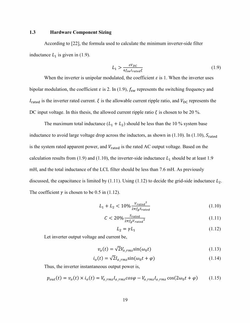
1.3 Hardware Component Sizing
According to [22], the formula used to calculate the minimum inverter-side filter
inductance .� is given in (1.9).
.� > \�&-]JK^_VY`WIa (1.9)
When the inverter is unipolar modulated, the coefficient b is 1. When the inverter uses
bipolar modulation, the coefficient b is 2. In (1.9), 0�c represents the switching frequency and
�deOf� is the inverter rated current. g is the allowable current ripple ratio, and �h� represents the
DC input voltage. In this thesis, the allowed current ripple ratio g is chosen to be 20 %.
The maximum total inductance (.� + .) should be less than the 10 % system base
inductance to avoid large voltage drop across the inductors, as shown in (1.10). In (1.10), ideOf�
is the system rated apparent power, and �deOf� is the rated AC output voltage. Based on the
calculation results from (1.9) and (1.10), the inverter-side inductance .� should be at least 1.9
mH, and the total inductance of the LCL filter should be less than 7.6 mH. As previously
discussed, the capacitance is limited by (1.11). Using (1.12) to decide the grid-side inductance ..
The coefficient j is chosen to be 0.5 in (1.12).
.� + . < 10% �VY`WI>:JD"VY`WI
(1.10)
@ < 20% "VY`WI:JD�VY`WI> (1.11)
. = j.� (1.12)
Let inverter output voltage and current be,
mR(n) = √2�R_5q7sin (tun) (1.13)
vR(n) = √2�R_5q7sin (tun + w) (1.14)
Thus, the inverter instantaneous output power is,
xRyS(n) = mR(n) × vR(n) = �R_5q7�R_5q7{|Bw − �R_5q7�R_5q7 cos(2tun + w) (1.15)

20
In (1.15), there is a double line frequency (2ω0) component in the inverter output power.
This double line frequency harmonic is also seen in the inverter input. Thus, a DC-link capacitor
should be utilized to limit the double grid line frequency voltage ripple at the inverter DC input.
Sufficient capacitance would help to lower DC-link voltage fluctuations and reduce the inverter
output current distortion, which is undesirable for power decoupling [7]. However, choosing an
oversized DC-link capacitor increases design cost. The following analysis shows how to size the
capacitance of a DC-link film capacitor for inverters.
Since the apparent power i5�S6G is,
i5�S6G = �R_5q7 × �R_5q7 (1.16)
Rewrite the output power as,
xRyS(n) = i5�S6G{|Bw + i5�S6G cos(2tun + w) (1.17)
The inverter input power is,
xCQ(n) ≅ �GT × ��GT + v5(n)� = �GT�GT + �GTv5(n) (1.18)
Neglecting circuit power loss,
xCQ(n) = xRyS(n) (1.19)
Since the DC-link capacitor filters out high frequency components, the double-line
frequency component is expressed as,
�GTv5(n) = i5�S6G cos (2tun + w) (1.20)
Thus, the double-line frequency current component at the DC side is,
v5(n) = "VY`WI�I�
cos(2tun + w) = �5cos (2tun + w) (1.21)
Assume the dc side maximum ripple voltage to be 5 % of the DC nominal voltage. The
minimum DC-link capacitance is calculated as,
@J = �5 2tu�5_q��⁄ = i5�S6G 4�0u�GT�5_q��⁄ (1.22)

21
Based on the analysis and calculations shown above, a minimum capacitance of 500 µF
capacitor is needed. All the parameters for the system is given in Table 1-1. The simulations
conducted in the following chapters are based on the parameters in Table 1-1.
Table 1-1: Designed parameters for the single-phase inverter
Parameter Value Parameter Value
DC bus ��� 400 V Sampling frequency 0� 30 kHz
Switching frequency 0�c 30 kHz .� 2 mH
@ 10 µF . 1 mH
@� 500 µF Resonance frequency 0df� 1.95 kHz

22
Chapter 2 Controller Design of Stand-Alone Inverter
Residential inverters are expected to be able to work off-grid to support critical loads as
uninterruptible power supplies. The design of a dual-loop controlled stand-alone inverter is
described in this chapter. The inner loop regulates current, and outer loop regulates inverter
output voltage across the capacitor of the filter. The inner current control loop can either regulate
the current flowing through the inverter-side inductor, or current flowing through the capacitor of
the filter. Since traditional PI controllers cannot achieve zero steady-state error while tracking
sinusoidal signals, direct quadrature (DQ) frame controllers and PR controllers are investigated
and applied. Using the synchronous frame outer control loop, a comparison on the control
performance between the two inner current feedback methods is performed. The island mode
inverter circuit and conventional control diagram is given in Fig. 2-1. Simulation results are
provided within this chapter.
Fig. 2-1: Island mode inverter circuit diagram
2.1 Inner Current Loop Design
Generally, the current inner loop has two options. One is to use the inverter-side inductor
current v�� as the feedback value [2]. The other one is to adopt the current flowing through
capacitor v� as the feedback value. The control diagrams of inner feedback systems using both
options are shown in Fig. 2-2 and Fig. 2-3, respectively. Comparing these two control diagrams,

23
it is seen that the capacitor current feedback control method includes the load current within the
control loop. Thus, by using capacitor current feedback method, the system can obtain better
performance when load changes. According to [2], the worst control design condition for stand-
alone inverter is in no load condition. Therefore, the load current is assumed to be zero in Fig. 2-
3. Thus, the control plants in Fig. 2-2 and Fig. 2-3 are identical.
Fig. 2-2: Inner control system diagram using inverter-side inductor current v�� feedback
Fig. 2-3: Inner control system diagram using capacitor current v� feedback
At least one switching period delay �� should be considered for digital implementation
since the modulation signal will not update until the next switching cycle [40]. The delay block
M� shown as (2.1) is a second order Pade approximation of the pure switching cycle delay.
According to the derived small-signal mode in [2, 43], the inverter stand-alone mode control
plant M� is given as (2.2). The control diagram shown in Fig. 2-3, the uncompensated inner
control loop plant can be derived as (2.3). A PI controller is used as the compensator for the
inner control loop. The compensated open loop is derived as (2.4) in the Laplace frequency
domain.

24
MG = $H7�K = �HL7�K=(7�K)>�=L7�K=(7�K)> (2.1)
M! = �7�< (2.2)
MC! = �!�qMGM! (2.3)
MC!_T = X�7=XE7 MC! (2.4)
The PI compensator is designed to boost the phase margin of the uncompensated transfer
function (2.3) to increase the system stability. The crossover frequency of the compensated
system should be less than one tenth of the switching frequency for good switching noise
rejection, and higher than ten times of the grid frequency for fast dynamics [4]. The desired
phase margin and gain margin are larger than 45 degrees and 7 dB, respectively. The
uncompensated and compensated Bode plots are shown in Fig. 2-4. The blue line is the Bode
plot of the uncompensated plant. The green line shows the open-loop Bode plot of the
compensated system. As we can see from Fig. 2-4, the phase margin is 48.4 degrees, the gain
margin is 8.14 dB, and the crossover frequency is designed to 2.9 kHz. The stability of the
compensated system is verified by Nyquist stability criterion. The PI compensator is given as
(2.5). The unit step response is shown in Fig. 2-5. The step response overshoot is 24.6 % and the
settling time is 0.831 ms.
Fig. 2-4: Bode plots of the uncompensated and compensated inner loop
Bode Diagram
Frequency (Hz)
101
102
103
104
105
106
-90
0
90
180
270
System: Gop_c
Phase Margin (deg): 48.4
Delay Margin (sec): 4.66e-05
At frequency (Hz): 2.89e+03
Closed loop stable? Yes
Phase (deg)
-100
-50
0
50
100
System: Compensated inner loop
Gain Margin (dB): 8.14
At frequency (Hz): 7.32e+03
Closed loop stable? Yes
Magnitude (dB
)
Uncompensated inner loop
Compensated inner loop
25
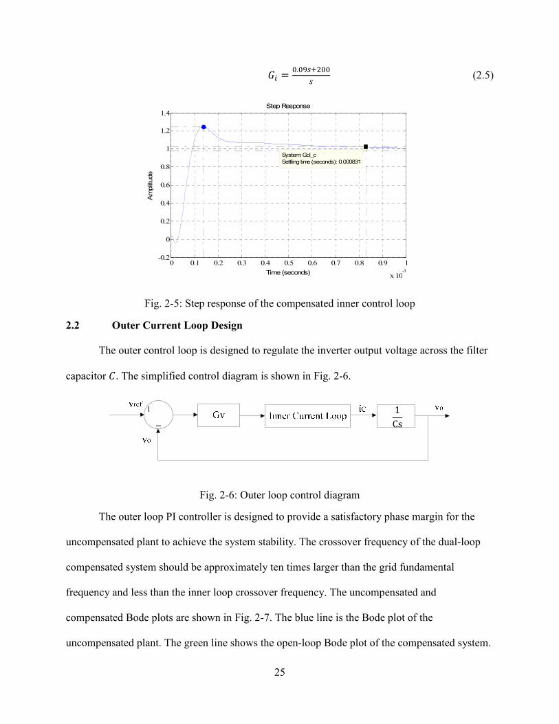
MC = u.u�7=uu7 (2.5)
Fig. 2-5: Step response of the compensated inner control loop
2.2 Outer Current Loop Design
The outer control loop is designed to regulate the inverter output voltage across the filter
capacitor @. The simplified control diagram is shown in Fig. 2-6.
1Cs
Fig. 2-6: Outer loop control diagram
The outer loop PI controller is designed to provide a satisfactory phase margin for the
uncompensated plant to achieve the system stability. The crossover frequency of the dual-loop
compensated system should be approximately ten times larger than the grid fundamental
frequency and less than the inner loop crossover frequency. The uncompensated and
compensated Bode plots are shown in Fig. 2-7. The blue line is the Bode plot of the
uncompensated plant. The green line shows the open-loop Bode plot of the compensated system.
Step Response
Time (seconds)
Am
plit
ude
0 0.1 0.2 0.3 0.4 0.5 0.6 0.7 0.8 0.9 1
x 10-3
-0.2
0
0.2
0.4
0.6
0.8
1
1.2
1.4
System: Gcl_c
Settling time (seconds): 0.000831

26
As we can see from Fig. 2-7, the phase margin is 62.2 degrees and the gain margin is 13.7 dB.
The crossover frequency is about 725 Hz. When the gain of the compensated open-loop system
is higher than 0 dB, there is no negative or positive phase crossing through the +/- 180º phase
line. The number of the compensated open-loop system RHP poles is zero. According to Nyquist
stability criterion, the compensated closed-loop system is stable. The PI compensator is given as
(2.6). The unit step response is shown in Fig. 2-8. The step response overshoot is 16.4 % and the
settling time is 2.32 ms. Apply the designed current loop PI controller and voltage loop PI
controller to the MatlabTM Simulink circuit model, the outer loop voltage tracking error is shown
in Fig. 2-9. The voltage tracking error shown in Fig. 2-9 has a peak value of 22 V at the
fundamental frequency. To eliminate the voltage tracking error, a synchronous rotating frame
DQ control [9] or a stationary reference frame proportional resonant control should be adopted
[7]. More detail is given in the following sessions.
Fig. 2-7: Bode plots of the uncompensated and compensated outer voltage loop
M% = u.u��7=�u7 (2.6)
-150
-100
-50
0
50
100
Magnitude (dB
)
System: Compensated outer loop
Gain Margin (dB): 13.7
At frequency (Hz): 3.63e+03
Closed loop stable? Yes
Bode Diagram
Frequency (Hz)
101
102
103
104
105
106
-180
-90
0
90
180
270
System: Compensated outer loop
Phase Margin (deg): 62.2
Delay Margin (sec): 0.000238
At frequency (Hz): 724
Closed loop stable? Yes
Phase (deg)
Uncompensated outer loop
Compensated outer loop

27
Fig. 2-8: Step response of the compensated outer voltage loop
Fig. 2-9: Dual-PI controlled inverter voltage tracking error
2.3 DQ Frame Control
Synchronous rotating frame DQ control can be used to eliminate tracking error for AC
quantities in dual-loop control systems [9, 10]. In the DQ rotating frame, the AC quantities in the
αβ stationary frame become DC quantities as the DQ frame rotates at the same fundamental
angular frequency as the AC quantities [2]. Traditional systems with DQ control method perform
both the current and voltage loops in synchronous rotating frame. Alternative methods have been
0 0.5 1 1.5 2 2.5 3 3.5 4 4.5 5
x 10-3
-0.2
0
0.2
0.4
0.6
0.8
1
1.2
System: Gvcl_c
Settling time (seconds): 0.00232
Step Response
Time (seconds)
Am
plit
ude
0 0.05 0.1 0.15 0.2-40
-30
-20
-10
0
10
20
30
40
Time (s)
Vol
tage
err
or (
V)
PI control
28
reported in [2, 9]. Those methods only apply DQ based control to outer voltage loop. The
obvious advantage of those methods is that those controls are easy to implement without
generating β components. The control diagram is shown in Fig. 2-10. The state-space form
equations shown as (2.7) and (2.8) describe the relationship between synchronous rotating frame
and stationary reference frame [9, 10].
Fig. 2-10: A DQ based control diagram of single-phase inverters
��G�� � = � cos (tn) sin (tn)−sin (tn) cos (tn)� ������ (2.7)
������ = �cos (tn) −sin (tn)sin (tn) cos (tn) � ��G��� (2.8)
Applying the DQ frame control to the single-phase H-bridge inverter, a comparison of the
control performance between the two inner current feedback methods (as shown in Fig. 2-2 and
Fig. 2-3) is performed. The comparison result is given in Fig. 2-11. At 0.05 s, the load changes to
1 kW from no load condition. The load reaches 2 kW at 0.1 s, and drops back to no load
condition at 0.15 s. The capacitor current feedback control method shown in Fig. 2-3 is adopted
since it provides more robust performance when load changes. In [2], the step load performance
is improved by adding an additional load current feedback besides the inverter-side inductor
current inner loop feedback. Doing so will increase the overall design cost since two current
sensors are utilized. The voltage and current responses with step load change are shown in Fig.
2-12 and Fig. 2-13, respectively. The voltage tracking error of the H-bridge inverter, where DQ
frame control is applied, is shown in Fig. 2-14. The total harmonics distortion (THD) of the

29
inverter voltage output is: 0.39 % with 1 kW load, 0.37 % with 2 kW load, and 0.40 % with no
load.
Fig. 2-11: Comparison of control performance between the two inner feedback methods
Fig. 2-12: Inverter output voltage
0.05 0.1 0.15 0.2-40
-20
0
20
40
60
80
100
Time (s)
Vol
tage
trac
king
err
or (
V)
Capacitor current feedbackInverter-side inductor current feedback
0 0.05 0.1 0.15 0.2-400
-200
0
200
400
Time (s)
Inve
rter
out
put v
olta
ge (
V)
Inverter output voltage
No load 1 kW load 2 kW load
No load

30
Fig. 2-13: Inverter output current
Fig. 2-14 shows that the DQ frame control enables the single-phase H-bridge inverter
control system to achieve zero steady-state tracking response. Thus, the DQ frame control
improves the inverter voltage output quality compared to the dual-PI control.
Fig. 2-14: Voltage tracking error comparison between PI control and DQ frame control
Generally, the power factor for a 2 kVA stand-alone inverter is between 0.707 and 1. The
inverter step load output performance with 1.4 kW resistive load and 1.4 kVar inductive load is
shown in Fig. 2-15. The THD of the inverter voltage output is 0.09 %. The inverter step load
output performance with 1.4 kW resistive load and 1.4 kVar capacitive load is displayed in Fig.
2-16. The THD of the inverter voltage output is 0.34 %.
0 0.05 0.1 0.15 0.2
-15
-10
-5
0
5
10
15
Time (s)
Inve
rter
out
put c
urre
nt (
A)
Inverter output current
2 kW load1 kW loadNo load No load
0 0.05 0.1 0.15 0.2-40
-30
-20
-10
0
10
20
30
40
Time (s)
Vol
tage
err
or (
V)
PI controlDQ based control

31
Fig. 2-15: Inverter output with 1.4 kVar inductive load and 1.4 kW resistive load
Fig. 2-16: Inverter output with 1.4 kVar capacitive load and 1.4 kW resistive load
2.4 Proportional Resonant Control
An alternative control method to achieve system zero steady-state error is using a
proportional resonant controller [44]. (2.9) shows the transfer function of a PR controller. The ��
is the proportional gain term and the �� parameter is the integral gain term. The tu is the
resonant angular frequency which is set to be the line angular frequency.
Fig. 2-17 and Fig. 2-18 are Bode plots of PR controllers with the same proportional gain
term and Bode plot of PR controllers with the same integral gain term, respectively. From Fig. 2-
0 0.05 0.1 0.15 0.2-400
-200
0
200
400
600
Time (s)
Am
plitud
e
20X Inverter output current (A)Grid voltage (V)
0 0.05 0.1 0.15 0.2-400
-200
0
200
400
600
Time (s)
Am
plitud
e
20X Inverter output (A)Grid voltage (V)
No load No load
No load No load

32
17 and Fig. 2-18, one can observe that the magnitude of the base of PR controller increases as the
integral gain term �� increases and the magnitude of the resonant part of the PR controller
accrues as the proportional gain term �� increases. It can also be seen that the PR controller can
provide infinite gain at the fundamental frequency which is the reason that PR controller can
eliminate steady-state tracking error. In the αβ stationary frame, a PR controller is equivalent to a
PI controller in the synchronous DQ frame. A detailed analysis is given in [2]. It is well known
that the PR controller described above is sensitive to resonance frequency drift due to the
implementation error caused by Tustin transformation [2]. The nonideal PR controller shown as
(2.10) provides a bandwidth for the resonant control part [44, 45]. A nonideal PR controller is
less sensitive to resonance frequency drift. The t� is the bandwidth around the resonance
frequency. Fig. 2-19 shows PR controllers with the same proportional gain term in the frequency
domain. Fig. 2-20 shows PR controllers with the same integral gain term in the frequency
domain.
M�,(B) = �! + XE77>=��>
(2.9)
Fig. 2-17: Bode plot of PR controllers with a fixed proportional gain term
0
100
200
300
400
Magnitude (dB)
100
101
102
103
104
-90
0
90
Phase (deg)
PR Bode Diagram, kp=3
Frequency (Hz)
ki = 400
ki = 600ki = 800

33
Fig. 2-18: Bode plot of PR controllers with a fixed integral gain term
M�,(B) = �! + 2�C ��77>=��7=��>
(2.10)
Fig. 2-19: Bode plot of nonideal PR controllers with a fixed proportional gain term
-100
0
100
200
300
Magnitude (
dB
)
10-1
100
101
102
103
104
-90
-45
0
45
90
Phase (
deg)
PR Bode Diagram, ki=100
Frequency (Hz)
kp = 0.1kp = 0.3kp = 0.5
0
20
40
60
Magnitude (
dB
)
10-1
100
101
102
103
104
-90
-45
0
45
90
Phase (
deg)
Nonideal PR Bode Diagram, kp=3
Frequency (Hz)
ki = 400ki = 600ki = 800
34
Fig. 2-20: Bode plot of nonideal PR controllers with a fixed integral gain term
To apply a nonideal PR controller to the outer voltage loop. The uncompensated and
compensated Bode plots are shown in Fig. 2-21. The blue line is the Bode plot of the
uncompensated plant. The green line shows the open-loop Bode plot of the compensated system
with nonideal PR control. As we can see from Fig. 2-21, the phase margin is 49.7 degrees and
the gain margin is 9.64 dB. The crossover frequency is approximately 1.1 kHz. The nonideal PR
controller is given by (2.9). The unit step response is shown in Fig. 2-22. The overshoot is
23.8 %, and the settling time is 1.17 ms. The closed-loop Bode diagram of the nonideal PR based
control is shown in Fig. 2-23. The voltage tracking error is given in Fig. 2-24. As we can see in
Fig. 2-24, the inverter output voltage achieves zero steady-state tracking error using the nonideal
PR control method. The nonideal PR control strategy can obtain the same control performance as
the DQ frame control method.
-20
0
20
40
60
Magnitude (
dB
)
10-1
100
101
102
103
104
105
-90
-45
0
45
90
Phase (
deg)
Nonideal PR Bode Diagram, ki=100
Frequency (Hz)
kp = 0.1kp = 0.3kp = 0.5

35
Fig. 2-21: Bode plots of the uncompensated and nonideal PR compensated outer voltage loop
M% = 0.06 + 35 ]77>=]7=(�u:)> (2.9)
Fig. 2-22: Step response of the compensated outer voltage loop with nonideal PR control
Bode Diagram
Frequency (Hz)
-200
-100
0
100
200
System: Compensated outer loop
Gain Margin (dB): 9.64
At frequency (Hz): 3.53e+03
Closed loop stable? YesM
agnitude (dB
)
10-1
100
101
102
103
104
105
106
-180
0
180
360
System: Compensated outer loop
Phase Margin (deg): 49.7
Delay Margin (sec): 0.000119
At frequency (Hz): 1.16e+03
Closed loop stable? YesPhase (deg)
Uncompensated outer loop
Compensated outer loop
0 0.5 1 1.5 2 2.5 3 3.5 4 4.5 5
x 10-3
-0.2
0
0.2
0.4
0.6
0.8
1
1.2
1.4
System: Gvcl_c
Settling time (seconds): 0.00117
Step Response
Time (seconds)
Am
plit
ude

36
Fig. 2-23: Closed-loop Bode plot of the dual-loop system with nonideal PR control
Fig. 2-24: Voltage tracking error comparison between PI control and nonideal PR control
2.5 Summary
In this chapter, the control design of a dual-loop controlled single-phase H-bridge
inverter in stand-alone operation mode is discussed. To eliminate the zero steady-state control
error, both the synchronous rotating frame with a DQ transformation and stationary reference
frame PR controller are investigated. However, the DQ frame control mentioned above is easier
for digital implementation, especially when the dual-loop PI controllers have already been
designed. Applying the DQ transformation to the outer voltage control loop, a simulation based
-150
-100
-50
0
50
Magnitude (dB
)
100
101
102
103
104
105
106
-180
0
180
360P
hase (deg)
Bode Diagram
Frequency (Hz)
0 0.05 0.1 0.15 0.2-40
-30
-20
-10
0
10
20
30
40
Time (s)
Vol
tage
err
or (
V)
PI controlPR control

37
comparison on the control performance between the two inner current feedback methods is
performed. Using the DQ transformation and capacitor current feedback, the designed controllers
can achieve both zero steady-state output voltage tracking error and good step load performance.
Table 2-1: Island mode inverter control comparison
Controller Zero steady-state error Load immunity Implementation
Conventional PI with inverter-side inductor current feedback
√ √ √√√
Conventional PI with capacitor current feedback
√ √√√ √√√
DQ based control with inverter-side inductor current feedback
√√√ √ √√
DQ based control with capacitor current feedback
√√√ √√√ √√
PR based control with inverter-side inductor current feedback
√√√ √ √
PR based control with capacitor current feedback
√√√ √√√ √

38
Chapter 3 Controller Design of Grid-Tied Inverter
Besides working as stand-alone power supplies, residential inverters are expected to send
extra generated power back to the utility. In this chapter, the control design of grid-tied inverters
is discussed and performed. In [12, 46-48], the grid-tied inverters are controlled as a voltage
source. However, the current output of the voltage controlled grid-tied inverter largely depends
on the grid voltage quality. In this thesis, the grid-tied mode inverter is seen as a current source
from the grid side, and the inverter output current is directly controlled. The proportional
capacitor current feedback method is used to achieve active damping for the inverter with an
LCL filter. The outer loop regulates the current flowing into the grid. A feed-forward loop is
adopted to reduce the grid fluctuation disturbances. For grid-tied inverters, sensing the grid
voltage phase information is necessary. An amplitude detection based method is investigated to
provide the in phase with the grid component and in quadrature phase with the grid component.
By utilizing amplitude detection method, no phase locked loop controller is needed. A PR
controller is adopted for outer control loop regulation to achieve the zero steady-state tracking
error in the grid-tied mode, as it is easy to implement active harmonics compensators (HC) in the
PR controller for better quality of the inverter output current [5]. The grid-connected mode
inverter circuit and control diagram is given in Fig. 3-1.
Fig. 3-1: Grid-tied inverter circuit diagram

39
3.1 Current Controller Design
As mentioned in Chapter 1, the capacitor current feedback loop with a simple
proportional controller �f is added to achieve active damping for the grid-tied inverter with an
LCL filter. Neglecting the feed-forward loop, the Laplace frequency domain block diagram of
the control method is illustrated in Fig. 3-2. The transfer function of the capacitor current �� to
the inverter output voltage �� is given in (3.1). The transfer function of the grid current �1 to the
inverter output voltage �� is given in (3.2). The inverter equivalent transfer function with one
switching period pure delay [40] is described as (3.3). Ignoring the internal resistance in
inductors, the transfer function (3.4) of the grid current �1 to the capacitor current �� is derived
from (3.1) and (3.2) [37]. The outer loop PR controller is shown as (3.5). For simplicity, the
harmonic compensators are not considered in the design process. However, they are used in
simulation and practical implementation.
Fig. 3-2: Grid-tied inverter control block diagram
M� = _�(7)�E(7) = �>?7
�<�>?7>=(�<=�>) (3.1)
M = _D(7)�E(7) = �
�<�>?7F=(�<=�>)7 (3.2)
M� = �!�qMG (3.3)
M] = _D(7)_�(7) = �
�>?7> (3.4)
MCR = M�,(B) = �!� + 2�C� ��<77>=��<7=(��)> (3.5)
The inner loop controller �f is related to the LCL filter damping performance. The outer
loop PR controller is designed to enlarge the phase margin and gain margin to ensure the stability

40
of the dual-loop control system. According to the guidance given in [28], the inner loop
controller gain �f is tuned to 0.08 for satisfactory damping. The Bode plot displayed as Fig. 3-3
shows how inner loop controller �f affects the damping performance. The Bode plots of the
compensated and uncompensated actively damped systems are shown in Fig. 3-4. By applying a
PR controller, the gain margin is increased to 11 dB and the phase margin of the system reaches
49 degrees. The crossover frequency of the compensated open-loop system is 658 Hz. The
number of the compensated open-loop system RHP poles is zero. According to Nyquist stability
criterion, the compensated closed-loop system is stable.
Fig. 3-3: Inner loop controller selection
Fig. 3-4: Bode plots of the compensated and uncompensated systems
Bode Diagram
Frequency (Hz)
-300
-200
-100
0
100
200
300
Magnitude (dB)
100
101
102
103
104
105
106
107
-360
-180
0
180
360
Phase (deg)
Ke = 0.08
No active damping
Ke = 0.001
Ke = 1.5
-200
-100
0
100
200
Magnitu
de (
dB
)
System: Compensated loop
Gain Margin (dB): 11
At f requency (Hz): 1.88e+003
Closed loop stable? Yes
100
101
102
103
104
105
106
-360
-180
0
180
360
Phas
e (
deg) System: Compensated loop
Phase Margin (deg): 49
Delay Margin (sec): 0.000207
At f requency (Hz): 658
Closed loop stable? Yes
Bode Diagram
Frequency (Hz)
Uncompensated loop
Compensated loop

41
The Bode diagram Fig. 3-5 shows that as proportional gain ��� decreases, the gain
margin increases, however, the crossover frequency and phase margin decreases. The practical
system may become unstable. The Bode plot in Fig. 3-6 illustrates that a higher integral gain of
PR controller ��� adds more negative phase shift around the resonance frequency, and a much
lower ��� degrade the high gain at the resonant frequency, which is set to be the grid frequency
60 Hz. Decreasing the high gain at the grid frequency results in a larger steady-state sinusoidal
tracking error. The designed controller is given as (3.6). With the designed controllers, when the
grid side inductance . changes within 50 %, which mimics the changes of the grid impedance,
the system is still robust as shown in Fig. 3-7.
MCR = M�,(B) = 0.032 + 6.4 77>=]7=��>
(3.6)
Fig. 3-5: Bode plots of the compensated systems with various ���
-200
-100
0
100
Magnitu
de (
dB
)
10-1
100
101
102
103
104
105
106
-360
-180
0
180
360
Phase (
deg)
Bode Diagram
Frequency (Hz)
Kp1 = 0.032
Kp1 = 0.008
Kp1 = 0.056

42
Fig. 3-6: Bode plots of the compensated systems with various ���
Fig. 3-7: Bode plots of the compensated systems with various .
With the designed controller, the system step response is given as in Fig. 3-8. The settling
time of the system response is 7.8 ms and the overshoot is 24 %. Fig. 3-9 shows the designed
control system tracks a 60 Hz sinusoidal signal with zero steady-state error. The blue line in Fig.
3-9 is the sinusoidal control reference.
-200
-100
0
100
Magnitude (
dB
)
100
101
102
103
104
105
106
-360
-180
0
180
360
Phase (
deg)
Bode Diagram
Frequency (Hz)
Ki1 = 3.2
Ki1 = 0.4
Ki1 = 6.8
-200
-100
0
100
Magnitude (dB
)
100
101
102
103
104
105
106
-360
-180
0
180
360
Phase (deg)
Bode Diagram
Frequency (Hz)
L2 = 1.0 mH
L2 = 1.5 mH
L2 = 0.5 mH

43
Fig. 3-8: Step response of the dual-loop control system
Fig. 3-9: Sinusoidal signal tracking response of the designed system
3.2 Phase Locked Loop and Amplitude Detection
In the grid-connected mode, it is essential to have a phase locked loop (PLL) module for
inverters. The PLL component takes measured grid AC voltage as a reference to generate an
estimated grid frequency t1¡ , and an estimated phase angle ¢£, in order to control the phase of the
inverter output signal. Thus, a PLL is a closed-loop servo system to minimize the output phase
0 0.002 0.004 0.006 0.008 0.01 0.012 0.014 0.016 0.018 0.020
0.2
0.4
0.6
0.8
1
1.2
1.4
Time (seconds)
Am
plit
ude
0 0.01 0.02 0.03 0.04 0.05 0.06 0.07 0.08 0.09 0.1-1.5
-1
-0.5
0
0.5
1
1.5
Time (seconds)
Am
plit
ude
Sinusoidal tracking response of the closed-loop system

44
and the reference phase error [49]. The PLL module performance affects the grid-connected
inverter operation directly.
Zero-crossing detection is a conventional phase tracking method. A zero-crossing based
PLL structure is given in Fig. 3-10. When the reference signal m1 passes zero towards to positive
value, ¢ is reset to 0. When the reference signal falls past zero, ¢ is reset to π. This type of PLL
module only detects reset points at half of the grid frequency. It is unable to provide good
dynamic performance. Moreover, the zero-crossing based PLL performance is susceptible to grid
harmonics and distortions. Thus, this kind of PLL is unfit for inverter grid-tied applications.
1s
¢£ 1s
t0
Fig. 3-10: Zero-crossing detection based PLL
Another PLL structure [50], which is commonly used for inverter grid-connected
applications, is shown in Fig. 3-11. The structure contains a phase detection (PD) unit, a low
bandwidth PI based loop filter (LF), and a voltage controlled oscillator (VCO). The PD unit is
used to detect the phase difference between the input signal and the reproduced output signal.
1s
¢£
t|
t¤¡
Fig. 3-11: Basic phase error detection based PLL
Let the input grid measurement be

45
m3(n) = √2�3_5q7 sin#¢3+ = √2�3_5q7sin (t3n + w3) (3.7)
The output signal of the PD unit is
m� (n) = √2�3_5q7sin (¢3)cos (¢£) (3.8)
To further expand (3.8), the m�h(n) can be expressed as,
m� (n) = √ �3_5q7sin �(t3 − t1¡)n + (w3 − w¥)� + √
�3V¦Ksin �(t1¡ + t3)n + (w¥ + w3)� (3.9)
The PD unit output signal is divided into a low frequency component and a high
frequency component as shown in (3.9). When the PD unit output signal passes through LF unit,
the high frequency component is filtered out. Then, the LF unit output is,
m��(n) = √ �3_5q7sin �(t3 − t1¡)n + (w3 − w¥)� (3.10)
Through the PI controller, the estimated frequency can be obtained. In the steady state,
m��(t) approaches to zero, as t1¡ = t1 and w¥ = w1. The phase of the output signal is locked with
the input grid measurement.
The PLL structure mentioned above has a LPF component in loop filter unit to filter out
double line frequency. An alternative way to realize PLL is to use a rotating reference frame PLL.
The PLL block diagram [12, 49] is shown below in Fig. 3-12. It consists of an orthogonal signal
generator (OSG), Park’s transform, a low bandwidth PI, and a VCO unit.
t¤¡
¨
t|
sin¢£
Fig. 3-12: OSG based single-phase PLL

46
The second order generalized integrator (SOGI) based OSG block, which is capable of
filtering out grid harmonics, contains a second order band pass filter (BPF) and a second order
low pass filter. The state-space form of the SOGI module is given in (3.11) and (3.12).
���©�© � = �−�!t3 −t3t3 0 � ����� + ��!t3
0 � ªm3« (3.11)
�m�m�� = �1 00 1� ����� (3.12)
A�(s) is defined as �¬(�)�(�), and A�(s) is defined as
�®(�)�(�) . The Bode plots of A�(s) and
A�(s) with variations of �� are shown in Fig. 3-13 and Fig. 3-14, respectively.
Fig. 3-13: Bode plot of A�(s)
-60
-40
-20
0
Magnitude (
dB
)
100
101
102
103
104
-90
-45
0
45
90
Phase (
deg)
Hd(s) Bode Diagram
Frequency (Hz)
Kp2 = 0.7Kp2 = 1.5Kp2 = 2.0

47
Fig. 3-14: Bode plot of A�(s)
Both Fig. 3-13 and Fig. 3-14 show that the parameter �� decides the OSG frequency
selectiveness and bandwidth. A smaller �� in the second order generalized integrator helps to
increase immunity to harmonics, but it can degrade the response of the SOGI [49]. Considering
the trade-off, �� is chosen to be 1.5 for simulations. Comparing Fig. 3-13 to Fig. 3-14, A�(s)
rejects the DC offset component in the sensed grid voltage, while A�(s) does not. Numerous
research projects [51, 52] have been done to enable A�(s) to reject the DC component in the
sensed grid voltage. In this design, a second order LPF is added into the SOGI based OSG loop
[51]. The original OSG structure [12] shown in Fig. 3-15 is then changed to the structure as in
Fig. 3-16.
-100
-50
0
50
Magnitude (
dB
)
100
101
102
103
104
-180
-90
0
Phase (
deg)
Hq(s) Bode Diagram
Frequency (Hz)
Kp2 = 0.7Kp2 = 1.5Kp2 = 2.0

48
t¤s
t¤s
Fig. 3-15: Second order generalized integrator for the OSG unit [12]
t¤s
t¤s
Fig. 3-16: Revised SOGI for the OSG unit
A second order LPF filter is described as
MJ = �#7 �¯⁄ +>=#7 °�¯⁄ +=� (3.13)
The cut-off frequency is chosen to be t� = 2�0� = 376.8 rad/s, and the quality factor ³
is set to be 0.71. The Laplace transfer function of the revised A�(s) is given as (3.14). The
revised Bode plot of A�(s) is illustrated in Fig. 3-17. By adding a second order LPF, A�(s) is
capable of rejecting the grid DC offset. Adding the second order LPF in the SOGI also increases
the ability of harmonic rejection. However, as the bandwidth becomes narrower, the response of
the SOGI becomes slower. It is a trade-off between frequency selectiveness and response speed.
A�(B)´ = A�(B) − MJ�!(B + t3) (B + �!t3B + t3)µ (3.14)

49
Fig. 3-17: Bode plot of A�(s)´
The grid amplitude can also be obtained through the SOGI-OSG module. The calculated
grid peak voltage is shown as (3.15).
¶�3¶ = (m� + m�)u.� (3.15)
Based on this grid peak voltage detection method [7, 53], the in phase with the grid and
in quadrature phase with the grid components can be achieved without the additional phase
locked loop. This method uses a constant t3 in (3.11), which is set to be grid angular frequency.
Considering the grid frequency changes slightly from 59.4 Hz to 60.6 Hz, according to IEEE-
1547 [54]. The error resulting from the grid peak detection method is negligible. The peak
amplitude detection based grid synchronization illustration diagram is shown in Fig. 3-18.
-150
-100
-50
0
50
Magnitude (
dB
)
100
101
102
103
104
-360
0
360
720
Phase (
deg)
Bode Diagram
Frequency (Hz)
Hq(s)Revised Hq(s) with 2nd order LPF, fc = 60 HzRevised Hq(s) with 1st order LPF, fc = 25 HzRevised Hq(s) with 1st order LPF, fc = 60 Hz

50
( )0.52 2v vα β+
Fig. 3-18: Peak detection based grid synchronization
The performance of the revised SOGI-OSG can be evaluated through various grid fault
conditions. Fig. 3-19 shows the performance of the revised SOGI on grid peak voltage detection
and quadrature signals generation when there is a frequency drift from 60 Hz to 60.6 Hz at 0.05 s.
The grid frequency recovers to nominal at 0.1 s. In Fig. 3-19, the black line represents the grid
voltage. The pink and blue lines represent the generated orthogonal signals. The red line shows
the calculated grid peak voltage. The settling time for peak detection is within two grid cycles. It
can be noticed that there is a double line frequency component in the detected peak voltage
during the grid frequency deviation. It is caused by setting t3 as the nominal grid angular
frequency in the revised SOGI module. The steady-state maximum voltage of the ripple is 341.5
V and the minimum voltage is 335 V.
Fig. 3-19: Revised SOGI performance under frequency drift
0 0.05 0.1 0.15-400
-200
0
200
400
600
Time (s)
Vol
tage
(V
)
Grid voltage Valpha Vbeta |Vg|

51
Fig. 3-20 shows the performance of the revised SOGI on grid peak voltage detection and
quadrature signals generation when the grid voltage drops to 90 % of nominal voltage at 0.05 s.
The grid voltage comes back to nominal at 0.1 s. The settling time for peak detection is also
within two grid cycles.
Fig. 3-20: Revised SOGI performance under voltage sag
Fig. 3-21 shows the performance of the revised SOGI on peak voltage detection and
quadrature signals generation when the grid voltage is polluted with harmonics and DC offset.
The grid voltage used for this simulation is given by (3.16). In Fig. 3-21, the black line shows the
polluted grid voltage. The pink and blue lines are the generated orthogonal signals. The red line
gives the calculated grid peak voltage. The settling time for peak detection is within two grid
cycles. In steady-state, the maximum voltage of the ripple is 347.7 V and the minimum voltage
of the ripple is 335.7 V. The calculated voltage deviated from the nominal grid peak voltage is
within 3 %.
m3 = 340(0.1 + sin#2�t3n+ + 0.05sin#2� × 3t3n+ + 0.05sin#2� × 5t3n+ +
0.03sin#2� × 7t3n+ + 0.01sin#2� × 9t3n+ + 0.01sin#2� × 23t3n+ (3.16)
0 0.05 0.1 0.15-400
-200
0
200
400
600
Time (s)
Vol
tage
(V
)
Grid voltage Valpha Vbeta |Vg|

52
Fig. 3-21: Revised SOGI performance under harmonics and DC offset polluted grid
3.3 Active and Reactive Power Flow Control
It is known that the inverter active power output is proportional to the current in phase
with the grid voltage, and the reactive power output is proportional to the current in quadrature
phase with the line voltage [45, 55]. Thus, the current reference v∗, as shown in (3.17), can be
divided into two components: active power current reference (v�∗) and reactive power current
reference (v¹∗ ). According to (3.18) and (3.19), (3.17) can be further expanded to (3.20).
Meanwhile, ��∗ and �¹∗ are the peak values of the current references and ¢ is estimated phase angle
of the grid voltage. With given specific active power and reactive power commands, the current
reference, which is used to control the single-phase inverter output current, can be obtained as
(3.21).
v∗ = v�∗ + v°∗ (3.17)
v�∗ = ��∗sin (¢) (3.18)
v°∗ = �°∗ cos (¢) (3.19)
v∗ = ��∗ sin(¢) + �°∗ cos (¢) (3.20)
v∗ = √2(�∗ ��N(º)�D + °∗ ���(º)
�D ) (3.21)
0 0.01 0.02 0.03 0.04 0.05 0.06 0.07 0.08-400
-200
0
200
400
600
Time (s)
Vol
tage
(V
)
Grid voltage Valpha Vbeta |Vg|

53
According to (3.21), a robust active power controller PI3 and reactive power controller
PI4 can be designed through the control block expressed in Fig. 3-22 and Fig. 3-23, respectively.
Fig. 3-22: PI based active power control loop
Fig. 3-23: PI based reactive power control loop
Instantaneous power estimation for active power and reactive power in stationary frame
can be obtained from (3.22) and (3.23) [45]. According to (3.20)-(3.23), a robust active and
reactive power controller can be expressed in Fig. 3-24.
» = (%D¼CD½=%D½CD¼) (3.22)
³ = (%D½CD¼H%D¼CD½) (3.23)
Fig. 3-24: Active and reactive power controller
There are three goals for designing the P controller and Q controller. The PQ control loop
system should be under damped with no overshoot. The active and reactive power adjustments
should be able to reach steady-state within three grid cycles. There should be zero steady-state

54
error for power commands tracking during the nominal grid condition. The designed P controller
and Q controller are given as (3.24) and (3.25), respectively.
M�_� = u.uuu��7=u.��7 (3.24)
M�_] = u.uuu��7=u.��7 (3.25)
3.4 Simulation Results
The grid-tied H-bridge inverter with designed controllers is simulated in MatlabTM
Simulink. The inverter is controlled by dual current control loop. The outer loop PR controller is
added with third, fifth, and seventh order harmonic compensation as shown in (3.26). The output
current of the inverter flowing into the grid is directly controlled by the reference generated from
the PQ controller to satisfy the expected output active and reactive power. The inverter output
current waveform is displayed in Fig. 3-25, when the inverter outputs 2000 W active power. The
THD of the inverter output current is 1.08 %. The steady-state tracking error between the current
reference signal and inverter current output is shown in Fig. 3-26. The result is also compared to
a simulation of the inverter with a PI based outer loop controller. The steady-state error is largely
reduced by using the designed PR controller. The inverter output active and reactive power
estimated by (3.22) and (3.23) are shown in Fig. 3-27 and Fig. 3-28, respectively. The settling
time for both active power and reactive power control is within 0.05 s.
MCR = M�,(B) = �!� + 2�C� ∑ ��<77>=��<7=(U��)>U¿�,�,�,Á (3.26)

55
Fig. 3-25: Inverter output current
Fig. 3-26: Steady-state tracking error of the inverter current controller
0.25 0.26 0.27 0.28 0.29 0.3 0.31 0.32 0.33 0.34 0.35-400
-200
0
200
400
600
Time (s)
Am
plitud
e
20X Inverter output current (A)Grid voltage (V)
0.1 0.2 0.3 0.4 0.5 0.6 0.7 0.8 0.9-8
-6
-4
-2
0
2
4
6
8
Time (s)
Cur
rent
err
or (
A)
PR based current control PI based current control

56
Fig. 3-27: Active power flow control performance
Fig. 3-28: Reactive power flow control performance
The grid may operate in numerous fault conditions. The grid frequency may drift slightly
between 59.4 Hz and 60.6 Hz [54]. The magnitude of the grid voltage can either drop to 90 %, or
swell to 110 % [54]. There may contain up to 0.1 % DC offset in the grid voltage [56]. The grid
can also contain higher order harmonics. The following simulations are completed during grid
distortion conditions.
0.2 0.4 0.6 0.8 1 1.2-500
0
500
1000
1500
2000
2500
Time (s)
Pow
er m
agni
tude
(W
)
Active power referenceInverter active power output
0.2 0.4 0.6 0.8 1 1.2-1500
-1000
-500
0
500
1000
1500
Time (s)
Rea
ctiv
e po
wer
mag
nitu
de (V
ar)
Reactive power referenceInverter reactive power output
Disturbance caused by
reactive power commands
Disturbance caused by
active power commands

57
The simulation results displayed in Fig. 3-29 and Fig. 3-30 show that the inverter
operates during frequency changes. The grid voltage and inverter output current are given in Fig.
3-29. The active power and reactive power are depicted in Fig. 3-30. At 0.1 s, the grid frequency
steps up to 60.6 Hz from 60 Hz. The grid frequency steps down to 60.3 Hz at 0.22 s. The THD of
the inverter output current is 1.87 % during 60.6 Hz frequency. The THD of the inverter output
current is 1.40 % during 60.3 Hz frequency.
Fig. 3-29: Grid voltage and inverter output current during frequency changes
Fig. 3-30: Calculated active and reactive power during frequency changes
0.05 0.1 0.15 0.2 0.25 0.3-400
-200
0
200
400
600
Time (s)
Mag
nitu
de
20X Inverter output current (A)Grid voltage (V)
0.05 0.1 0.15 0.2 0.25 0.3-500
0
500
1000
1500
2000
Time (s)
Mag
nitu
de
Active power (W)Reactive power (Var)

58
The simulation results displayed in Fig. 3-31 and Fig. 3-32 show that the inverter
operates during 10 % voltage sag. The grid voltage and inverter output current are given in Fig.
3-31. The instantaneous active power and reactive power are depicted in Fig. 3-32. At 0.1 s, the
grid magnitude drops to 90 % of nominal voltage, and it recovers back to 240 V at 0.22 s. The
THD of the inverter output current is 0.99 % during the voltage sag.
Fig. 3-31: Grid voltage and inverter output current during voltage sag
Fig. 3-32: Calculated active and reactive power during voltage sag
0.05 0.1 0.15 0.2 0.25 0.3-400
-200
0
200
400
600
Time (s)
Mag
nitu
de
20X Inverter output current (A)Grid voltage (V)
0.05 0.1 0.15 0.2 0.25 0.3-500
0
500
1000
1500
2000
Time (s)
Mag
nitu
de
Active power (W)Reactive power (Var)

59
The grid can be polluted by up to 0.1 % DC offset [56]. However, voltage sensing
circuits can also introduce DC offset to a certain level to introduce substantial DC components in
the inverter output current. The grid voltage and inverter output current are shown in Fig. 3-33.
The instantaneous active power and reactive power are given in Fig. 3-34. The grid voltage is
polluted by 5 % of the nominal grid voltage DC component at 0.1 s, and it recovers back to
nominal grid voltage at 0.22 s. The THD of the inverter output current is 1.21 % during the
period where the grid is injected by DC components.
Fig. 3-33: Grid voltage and inverter output current under DC influence
Fig. 3-34: Calculated active and reactive power under DC influence
0.05 0.1 0.15 0.2 0.25 0.3-400
-200
0
200
400
600
Time (s)
Mag
nitu
de
20X Inverter output current (A)Grid voltage (V)
0.05 0.1 0.15 0.2 0.25 0.3-500
0
500
1000
1500
2000
Time (s)
Mag
nitu
de
Active power (W)Reactive power (Var)

60
The simulation results displayed in Fig. 3-35 and Fig. 3-36 show that the inverter
operates during the grid polluted by 3 % third order, 2 % fifth order, and 1 % seventh order
harmonics. Grid voltage and inverter output current are given in Fig. 3-35. The instantaneous
active power and reactive power are displayed in Fig. 3-36. The harmonics injected grid
condition starts at 0.1 s and ends at 0.22 s. The THD of the inverter output current is 1.87 %.
Fig. 3-35: Grid voltage and inverter output current under grid distortion
Fig. 3-36: Calculated active and reactive power under grid distortion
0.05 0.1 0.15 0.2 0.25 0.3-400
-200
0
200
400
600
Time (s)
Mag
nitu
de
20X Inverter output current (A)Grid voltage (V)
0.05 0.1 0.15 0.2 0.25 0.3-500
0
500
1000
1500
2000
Time (s)
Mag
nitu
de
Active power (W)Reactive power (Var)

61
3.5 Summary
In this chapter, the control design of a grid-connected single-phase H-bridge inverter has
been discussed. The grid synchronization is achieved based on the grid peak amplitude detection
through a revised orthogonal signal generation. Since the grid phase angle is not provided
directly, a PR controller with harmonic compensations is adopted over a DQ frame control to
achieve the zero steady-state inverter output current. A PQ controller with stable and robust
performance is also described. Based on the simulation results, the active and reactive power can
be well controlled and decoupled under various grid fault conditions such as grid frequency drift,
grid voltage sag and swell, and grid voltage distortion.
62
Chapter 4 Experimental Test Results
4.1 Experimental Test Station
To validate the control design performed in previous chapters, a scaled-down prototype,
as shown in Fig. 4-1, is constructed. The parameters used are given in Table 4-1. The H-bridge is
built with evaluation boards from Cree○R [57]. The LCL filter and sensing circuits are built on
breadboards. A DC supply has been used to provide the high DC voltage bus. The controllers
and serial communications are implemented on a 32-bit float point digital controller, TI’s
F28335. A variable transformer is connected between the inverter and the grid for grid-tied
inverter mode test to provide isolation. Off-grid and On-grid tests are conducted.
Fig. 4-1: Experiment test station of a single-phase inverter with LCL filter
Table 4-1: Parameters used for experimental test
Parameter Value Parameter Value
DC bus ��� 200/400 V Sampling frequency 0� 30 kHz
Switching frequency 0�c 30 kHz .� 2.2 mH
@ 9.8 µF . 1.1 mH
LCL Filter and Sensors
H-Bridge Inverter
DSP
Load Grid
Communications
DC Supply
DC Link

63
4.1.1 Stand-Alone Mode
This section shows the test results of the stand-alone inverter operation. As discussed in
Chapter 2, the synchronous frame PI control is implemented. The inverter is tested to output 120
VAC and 240 VAC when the DC bus is 200 VDC and 400 VDC, respectively. The closed-loop
inverter with 120 VAC output at no load condition is shown in Fig. 4-2. In Fig. 4-2, CH1 (100
V/div) is the inverter output voltage, CH2 (40 V/div) is the DC supply voltage, CH3 (2 A/div) is
the load current, and CH4 (1 A/div) is the DC supply current. When the inverter generates 120
VAC output with no load, the THD of the inverter output voltage is 3.93 %, as shown in Fig. 4-3.
Fig. 4-2: 120 VAC stand-alone inverter output with no load (synchronous frame PI)
Fig. 4-3: The THD of the stand-alone inverter output with no load at 120 VAC
Vinv iinv VDC iDC
64
When a 135 W resistive load is added to the inverter output, the steady-state performance
of the inverter is shown in Fig. 4-4. The THD of the inverter output voltage is 2.56 % when the
inverter is connected with a 135 W resistive load, as shown in Fig. 4-5.
Fig. 4-4: 120 VAC stand-alone inverter output with a 135 W load
Fig. 4-5: The THD of the120 VAC stand-alone inverter output with a 135 W load
The load step transient response of the inverter output from no load to a 135 W load is
given in Fig. 4-6.
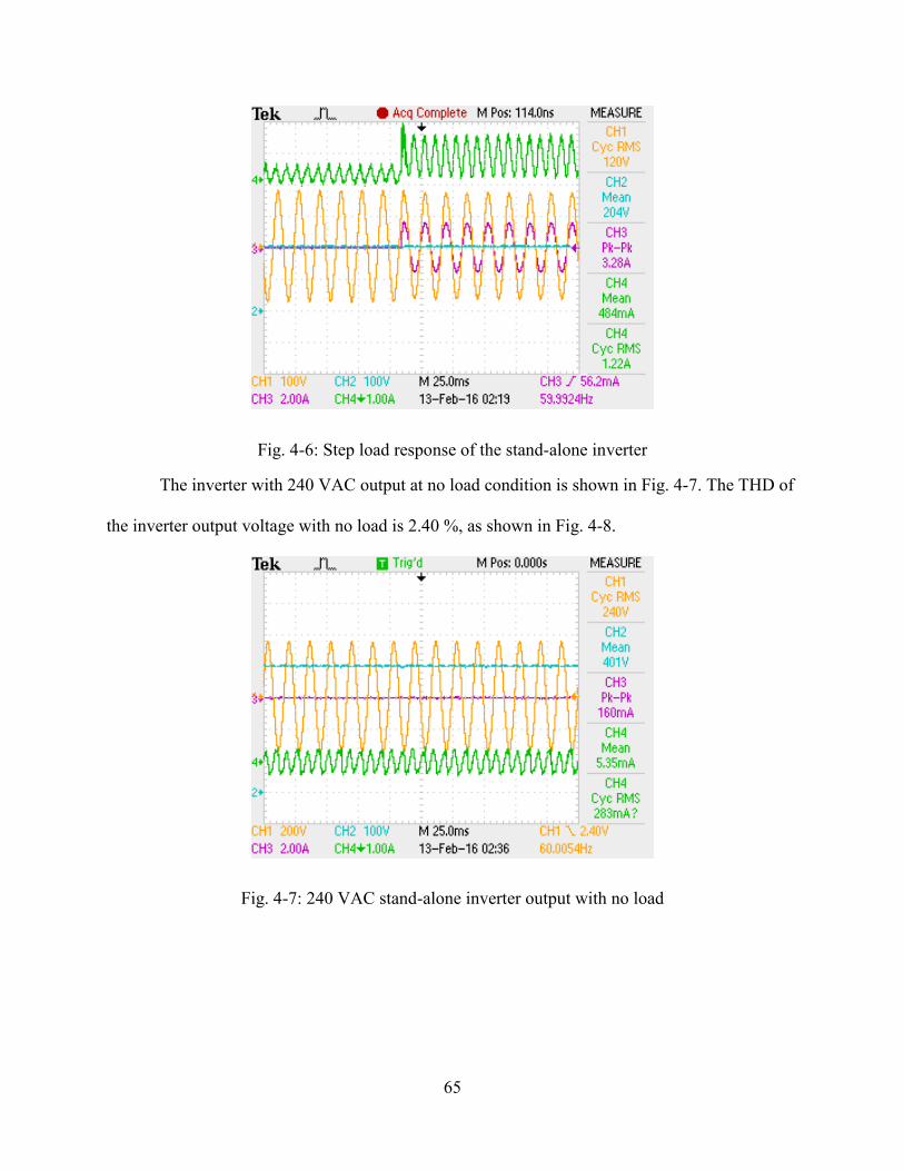
65
Fig. 4-6: Step load response of the stand-alone inverter
The inverter with 240 VAC output at no load condition is shown in Fig. 4-7. The THD of
the inverter output voltage with no load is 2.40 %, as shown in Fig. 4-8.
Fig. 4-7: 240 VAC stand-alone inverter output with no load

66
Fig. 4-8: The THD of the stand-alone inverter output with no load at 240 VAC
When a 500 W resistive load to the inverter output, the steady-state performance of the
inverter is shown in Fig. 4-9. The measured system efficiency is 94.9 %. The load step transient
response of the inverter output from no load to a 500 W load is given in Fig. 4-10.
Fig. 4-9: 240 VAC stand-alone inverter output with a 500 W load
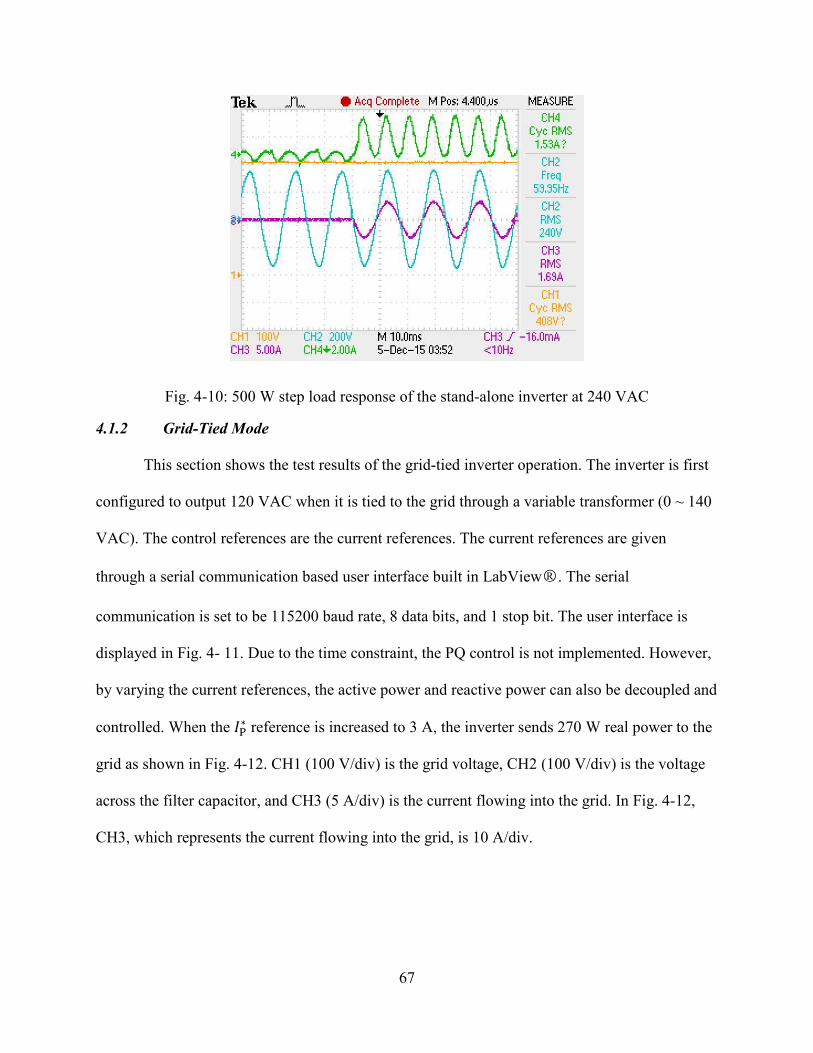
67
Fig. 4-10: 500 W step load response of the stand-alone inverter at 240 VAC
4.1.2 Grid-Tied Mode
This section shows the test results of the grid-tied inverter operation. The inverter is first
configured to output 120 VAC when it is tied to the grid through a variable transformer (0 ~ 140
VAC). The control references are the current references. The current references are given
through a serial communication based user interface built in LabView○R . The serial
communication is set to be 115200 baud rate, 8 data bits, and 1 stop bit. The user interface is
displayed in Fig. 4- 11. Due to the time constraint, the PQ control is not implemented. However,
by varying the current references, the active power and reactive power can also be decoupled and
controlled. When the ��∗ reference is increased to 3 A, the inverter sends 270 W real power to the
grid as shown in Fig. 4-12. CH1 (100 V/div) is the grid voltage, CH2 (100 V/div) is the voltage
across the filter capacitor, and CH3 (5 A/div) is the current flowing into the grid. In Fig. 4-12,
CH3, which represents the current flowing into the grid, is 10 A/div.

68
Fig. 4-11: Serial communication based user interface
Fig. 4-12: Grid-tied inverter with 270 W output (PR+HC control)
As discussed in Chapter 3, the inverter can also handle delivering or sinking reactive
power. Keeping the active power output constant and varying the �¹∗ reference to 2 A, the
inverter sends 269 W real power and 180 Var to the grid as shown in Fig. 4-13. Negating the
current reference �¹∗ , the inverter is able to receive 178 Var from the grid as displayed in Fig. 4-
14. Fig. 4-15 shows the THD of the inverter output current at the current condition is 4.32 %.
Vgrid (THD=5.32 %)
igrid

69
Fig. 4-13: Grid-tied inverter with 269 W and 180 Var output
Fig. 4-14: Grid-tied inverter with 267 W and -178 Var output

70
Fig. 4-15: The THD of the inverter output current
The inverter is then tied with the grid at 240 VAC. When the ��∗ reference is set to be 4.5
A, the inverter sends 750 W real power to the grid with 0.99 power factor, as shown in Fig. 4-16.
CH1 (200 V/div) is the grid voltage, CH2 (10 A/div) is the inverter output current, and CH4 (100
V/div) is the high voltage DC bus. The THD of the inverter current is 3.71 %, as shown in Fig. 4-
17.
Fig. 4-16: Grid-tied inverter with 750 W output

71
Fig. 4-17: The THD of the inverter output current (750 W)
The inverter is also tested to deliver reactive power and to sink reactive power. Fig. 4-18
shows the experimental result when the ��∗ reference is set to be 4.0 A, and the �¹∗ reference is set
to be 2.0 A. In Fig. 4-18, the inverter outputs 663 W real power and 324 Var reactive power to
the grid. The power factor is 0.90 lagging, and the phase angle difference between inverter
output voltage and current is 26.04º.
Fig. 4-18: Inverter current output with 0.90 lagging power factor

72
Fig. 4-19 shows the experimental result when the ��∗ reference is set to be 4.0 A, and the
�¹∗ reference is set to be -1.0 A. In Fig. 4-19, the inverter outputs 618 W real power and sinks 193
Var reactive power to the grid. The power factor is 0.95 leading, and the phase angle difference
between inverter output voltage and current is 17.33º.
Fig. 4-19: Inverter current output with 0.95 leading power factor

73
Chapter 5 Conclusion and Future Work
5.1 Conclusion
This thesis presented controls of a single-phase inverter for residential PV application.
This thesis reviewed solar energy, PV inverter configurations, and inverter filter topologies.
Passive hardware component parameters design was discussed. Controllers were designed for
both stand-alone mode and grid-tied mode single-phase inverter. The modeling and control
design were verified by the simulation and experimental results. For stand-alone inverter control,
the outer control loop regulates the filter capacitor voltage. As to the inner loop feedback signal,
a comparison was made between choosing the inverter-side inductor current and using the
capacitor current. Theoretically, the load current is included within the inner control loop when
using the filter capacitor current feedback. Therefore, the system can achieve more robust
transient response during load changes. This analysis was verified in the simulation, which
showed that regulating the capacitor current as the inner loop had a superior transient response
when the resistive load changes. Synchronous frame DQ control and PR control were proposed
in other previous publications for systems to achieve zero steady-state error when tracking
sinusoidal references. The zero steady-state tracking performance was verified by the simulation
and experimental test performed in this project. Using the designed control, both the simulation
and experimental results showed that the THD of the inverter output voltage, which is less than
5 %, satisfied IEEE 519-1992 standard. For grid-tied inverter control, the proportional capacitor
current feedback is used to achieve active damping. The outer current loop directly regulates the
current that goes to the grid. A serial communication based user interface is developed to feed
the control references. With the designed PR controller, the current injected into the grid could
accurately follow the given sinusoidal control references in both simulation and experimental test.

74
Several PLL methods have been reviewed and analyzed, and the SOGI based grid
synchronization has been chosen for its superior harmonic filtering capability, fast response, and
simplicity. The simulation and test results validated that the active power and reactive power
were decoupled with the grid synchronization unit and the reactive power could be either
injected into the grid or absorbed from the grid. In the test, the maximum reactive power
absorbed from the grid is 299 VAR, and the maximum reactive power sent out to the grid is 435
VAR. The tested power factor ranges from 0.86 leading to 0.80 lagging. Both the simulation and
experimental results showed that the THD of the grid-tied inverter output current, which is less
than 5 %, satisfied IEEE 519-1992 and 1547 standards for distributed resources.
5.2 Future Work
This project can be continued and extended to design a high efficiency DC/DC converter
stage and a reliable MPPT technique as future work. Seamless transitions between island mode
and grid-tied mode need to be developed. To realize the transitions, the frequency estimation of
the grid voltage will be needed. In addition, a practical PCB can be created for the rated power
inverter. The PQ controller developed in the simulation can also be implemented in the hardware.
For future experimental test, PV modules can be used and the DC bus can be provided by the
DC/DC conversion stage instead of a DC supply. When PV modules are used, the range of
reactive power compensation needs to be revaluated due to the equivalent impedance change on
the DC side. The project can also extend to design energy storage units like batteries and super
capacitors to store the harvested solar energy for utilization at night. Furthermore, the serial
communication can also be improved and replaced by Ethernet communication for extended
connectivity and faster communication speed. Since the active power and reactive power can be
controlled, research on power management can also be conducted as future work.
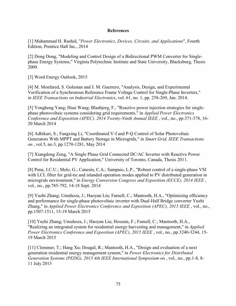
75
References
[1] Muhammad H. Rashid, "Power Electronics, Devices, Circuits, and Applications", Fourth Edition, Prentice Hall Inc., 2014
[2] Dong Dong, "Modeling and Control Design of a Bidirectional PWM Converter for Single-phase Energy Systems," Virginia Polytechnic Institute and State University, Blacksburg, Thesis 2009.
[3] Word Energy Outlook, 2015
[4] M. Monfared, S. Golestan and J. M. Guerrero, "Analysis, Design, and Experimental Verification of a Synchronous Reference Frame Voltage Control for Single-Phase Inverters," in IEEE Transactions on Industrial Electronics, vol. 61, no. 1, pp. 258-269, Jan. 2014.
[5] Yongheng Yang; Huai Wang; Blaabjerg, F., "Reactive power injection strategies for single-phase photovoltaic systems considering grid requirements," in Applied Power Electronics
Conference and Exposition (APEC), 2014 Twenty-Ninth Annual IEEE , vol., no., pp.371-378, 16-20 March 2014
[6] Adhikari, S.; Fangxing Li, "Coordinated V-f and P-Q Control of Solar Photovoltaic Generators With MPPT and Battery Storage in Microgrids," in Smart Grid, IEEE Transactions
on , vol.5, no.3, pp.1270-1281, May 2014
[7] Xiangdong Zong, "A Single Phase Grid Connected DC/AC Inverter with Reactive Power Control for Residential PV Application," University of Toronto, Canada, Thesis 2011.
[8] Pena, J.C.U.; Melo, G.; Canesin, C.A.; Sampaio, L.P., "Robust control of a single-phase VSI with LCL filter for grid-tie and islanded operation modes applied to PV distributed generation in microgrids environment," in Energy Conversion Congress and Exposition (ECCE), 2014 IEEE , vol., no., pp.785-792, 14-18 Sept. 2014
[9] Yuzhi Zhang; Umuhoza, J.; Haoyan Liu; Farnell, C.; Mantooth, H.A., "Optimizing efficiency and performance for single-phase photovoltaic inverter with Dual-Half Bridge converter Yuzhi Zhang," in Applied Power Electronics Conference and Exposition (APEC), 2015 IEEE , vol., no., pp.1507-1511, 15-19 March 2015
[10] Yuzhi Zhang; Umuhoza, J.; Haoyan Liu; Hossain, F.; Farnell, C.; Mantooth, H.A., "Realizing an integrated system for residential energy harvesting and management," in Applied
Power Electronics Conference and Exposition (APEC), 2015 IEEE , vol., no., pp.3240-3244, 15-19 March 2015
[11] Clemmer, T.; Hang Xu; Dougal, R.; Mantooth, H.A., "Design and evaluation of a next generation residential energy management system," in Power Electronics for Distributed
Generation Systems (PEDG), 2013 4th IEEE International Symposium on , vol., no., pp.1-8, 8-11 July 2013

76
[12] Minsoo Jang; Ciobotaru, M.; Agelidis, V.G., "A Single-Phase Grid-Connected Fuel Cell System Based on a Boost-Inverter," in Power Electronics, IEEE Transactions on , vol.28, no.1, pp.279-288, Jan. 2013
[13] Hanju Cha; Trung-Kien Vu, "Comparative analysis of low-pass output filter for single-phase grid-connected Photovoltaic inverter," in Applied Power Electronics Conference and
Exposition (APEC), 2010 Twenty-Fifth Annual IEEE , vol., no., pp.1659-1665, 21-25 Feb. 2010
[14] H. C. Chiang and H. Y. Tsai, "Design and implementation of a grid-tied wind power micro-inverter," in IET Renewable Power Generation, vol. 7, no. 5, pp. 493-503, Sept. 2013.
[15] Esram, T.; Chapman, P.L., "Comparison of Photovoltaic Array Maximum Power Point Tracking Techniques," in Energy Conversion, IEEE Transactions on , vol.22, no.2, pp.439-449, June 2007
[16] Sera, D.; Mathe, L.; Kerekes, T.; Spataru, S.V.; Teodorescu, R., "On the Perturb-and-Observe and Incremental Conductance MPPT Methods for PV Systems," in Photovoltaics, IEEE
Journal of , vol.3, no.3, pp.1070-1078, July 2013
[17] David S. M., "Maximum Power Point Tracking Algorithms for Photovoltaic Applications," Aalto University, Finland, Thesis 2010.
[18] Komurcugil, H., "Steady-State Analysis and Passivity-Based Control of Single-Phase PWM Current-Source Inverters," in Industrial Electronics, IEEE Transactions on , vol.57, no.3, pp.1026-1030, March 2010
[19] Weimin Wu; Yuanbin He; Tianhao Tang; Blaabjerg, F., "A New Design Method for the Passive Damped LCL and LLCL Filter-Based Single-Phase Grid-Tied Inverter," in Industrial
Electronics, IEEE Transactions on , vol.60, no.10, pp.4339-4350, Oct. 2013
[20] Akagi, H., "Active Harmonic Filters," in Proceedings of the IEEE , vol.93, no.12, pp.2128-2141, Dec. 2005
[21] Weimin Wu; Yuanbin He; Blaabjerg, F., "An LLCL Power Filter for Single-Phase Grid-Tied Inverter," in Power Electronics, IEEE Transactions on , vol.27, no.2, pp.782-789, Feb. 2012
[22] Bhardwaj, M.; Choudhury, S.; Xue, V.; Akin, B., "Online LCL filter compensation using embedded FRA," in Applied Power Electronics Conference and Exposition (APEC), 2014
Twenty-Ninth Annual IEEE , vol., no., pp.3186-3191, 16-20 March 2014
[23] Sosa, J.M.; Escobar, G.; Martinez-Rodriguez, P.R.; Vazquez, G.; Juarez, M.A.; Diosdado, M., "Comparative evaluation of L and LCL filters in transformerless grid tied converters for active power injection," in Power, Electronics and Computing (ROPEC), 2014 IEEE
International Autumn Meeting on , vol., no., pp.1-6, 5-7 Nov. 2014
77
[24] Liserre, M.; Blaabjerg, F.; Hansen, S., "Design and control of an LCL-filter-based three-phase active rectifier," in Industry Applications, IEEE Transactions on , vol.41, no.5, pp.1281-1291, Sept.-Oct. 2005
[25] Blooming, T.M.; Carnovale, D.J., "Application of IEEE STD 519-1992 Harmonic Limits," in Pulp and Paper Industry Technical Conference, 2006. Conference Record of Annual , vol., no., pp.1-9, 18-23 June 2006
[26] Chenlei Bao; Xinbo Ruan; Xuehua Wang; Weiwei Li; Donghua Pan; Kailei Weng, "Step-by-Step Controller Design for LCL-Type Grid-Connected Inverter with Capacitor–Current-Feedback Active-Damping," in Power Electronics, IEEE Transactions on , vol.29, no.3, pp.1239-1253, March 2014
[27] Lopez, O.; Freijedo, F.D.; Yepes, A.G.; Fernandez-Comesaa, P.; Malvar, J.; Teodorescu, R.; Doval-Gandoy, J., "Eliminating Ground Current in a Transformerless Photovoltaic Application," in Energy Conversion, IEEE Transactions on , vol.25, no.1, pp.140-147, March 2010
[28] S. G. Parker, B. P. McGrath and D. G. Holmes, "Regions of Active Damping Control for LCL Filters," in IEEE Transactions on Industry Applications, vol. 50, no. 1, pp. 424-432, Jan.-Feb. 2014.
[29] S. G. Parker, B. P. McGrath and D. G. Holmes, "Regions of active damping control for LCL filters," Energy Conversion Congress and Exposition (ECCE), 2012 IEEE, Raleigh, NC, 2012, pp. 53-60.
[30] Donghua Pan; Xinbo Ruan; Xuehua Wang; Chenlei Bao; Weiwei Li, "Robust capacitor-current-feedback active damping for the LCL-type grid-connected inverter," in Energy
Conversion Congress and Exposition (ECCE), 2013 IEEE , vol., no., pp.728-735, 15-19 Sept. 2013
[31] Chenlei Bao; Xinbo Ruan; Xuehua Wang; Weiwei Li; Donghua Pan; Kailei Weng, "Design of injected grid current regulator and capacitor-current-feedback active-damping for LCL-type grid-connected inverter," in Energy Conversion Congress and Exposition (ECCE), 2012 IEEE , vol., no., pp.579-586, 15-20 Sept. 2012
[32] Xuehua Wang; Chenlei Bao; Xinbo Ruan; Weiwei Li; Donghua Pan, "Design Considerations of Digitally Controlled LCL-Filtered Inverter With Capacitor- Current-Feedback Active Damping," in Emerging and Selected Topics in Power Electronics, IEEE Journal of , vol.2, no.4, pp.972-984, Dec. 2014
[33] Xu, A.J.; Xie, B.S.; Kan, C.J.; Zhang, D.B., "Research on stability of grid-connected LCL-filtered inverter with capacitor current feedback active damping control," in Power Electronics
and ECCE Asia (ICPE-ECCE Asia), 2015 9th International Conference on , vol., no., pp.682-687, 1-5 June 2015
[34] Xiongfei Wang; Blaabjerg, F.; Poh Chiang Loh, "Design-oriented analysis of resonance damping and harmonic compensation for LCL-filtered voltage source converters," in Power

78
Electronics Conference (IPEC-Hiroshima 2014 - ECCE-ASIA), 2014 International , vol., no., pp.216-223, 18-21 May 2014
[35] Dannehl, J.; Fuchs, F.W.; Hansen, S.; Thøgersen, P.B., "Investigation of Active Damping Approaches for PI-Based Current Control of Grid-Connected Pulse Width Modulation Converters With LCL Filters," in Industry Applications, IEEE Transactions on , vol.46, no.4, pp.1509-1517, July-Aug. 2010
[36] Hahn Durgante, M.; Batista Plotzki, H.F.; Stefanello, M., "Combined active damping with adaptive current control for converters with LCL filters," in Industrial Electronics Society,
IECON 2013 - 39th Annual Conference of the IEEE , vol., no., pp.520-525, 10-13 Nov. 2013
[37] Yang Han; Zipeng Li; Guerrero, J.M., "Dynamic evaluation of LCL-type grid-connected inverters with different current feedback control schemes," in Power Electronics and ECCE Asia
(ICPE-ECCE Asia), 2015 9th International Conference on , vol., no., pp.391-396, 1-5 June 2015
[38] Wenli Yao; Yongheng Yang; Xiaobin Zhang; Blaabjerg, F., "Digital notch filter based active damping for LCL filters," in Applied Power Electronics Conference and Exposition
(APEC), 2015 IEEE , vol., no., pp.2399-2406, 15-19 March 2015
[39] Young-Chan Cho; Ki-Young Choi; Rae-Young Kim, "Adaptive damping scheme of LCL filter resonance under inductance variation for a single-phase grid-connected inverter," in Power
Electronics and ECCE Asia (ICPE-ECCE Asia), 2015 9th International Conference on , vol., no., pp.978-983, 1-5 June 2015
[40] Yuanbin He; Ke-wei Wang; Chung, H.S.-H., "Utilization of proportional filter capacitor voltage feedforward to realize active damping for digitally-controlled grid-tied inverter operating under wide grid impedance variation," in Energy Conversion Congress and Exposition (ECCE),
2014 IEEE , vol., no., pp.4450-4457, 14-18 Sept. 2014
[41] Jinming Xu; Shaojun Xie; Ting Tang, "Active Damping-Based Control for Grid-Connected LCL-Filtered Inverter With Injected Grid Current Feedback Only," in Industrial
Electronics, IEEE Transactions on , vol.61, no.9, pp.4746-4758, Sept. 2014
[42] Xiongfei Wang; Blaabjerg, F.; Poh Chiang Loh, "Grid-Current-Feedback Active Damping for LCL Resonance in Grid-Connected Voltage-Source Converters," in Power Electronics, IEEE
Transactions on , vol.31, no.1, pp.213-223, Jan. 2016
[43] Chen, Chien-Liang; Jih-Sheng Lai; Yu-Bin Wang; Sung-Yeul Park; Miwa, H., "Design and Control for LCL-Based Inverters with Both Grid-Tie and Standalone Parallel Operations," in Industry Applications Society Annual Meeting, 2008. IAS '08. IEEE , vol., no., pp.1-7, 5-9 Oct. 2008
[44] Chattopadhyay, R.; De, A.; Bhattacharya, S., "Comparison of PR controller and damped PR controller for grid current control of LCL filter based grid-tied inverter under frequency variation and grid distortion," in Energy Conversion Congress and Exposition (ECCE), 2014 IEEE , vol., no., pp.3634-3641, 14-18 Sept. 2014

79
[45] Chi Yao Wu; Ching Heng Chen; Jhe Wei Cao; MingTai Liu, "Power control and pulsation decoupling in a single-phase grid-connected voltage-source inverter," in TENCON Spring
Conference, 2013 IEEE , vol., no., pp.475-479, 17-19 April 2013
[46] Matas, J.; Castilla, M.; de Vicuña, L.G.; Miret, J.; Vasquez, J.C., "Virtual Impedance Loop for Droop-Controlled Single-Phase Parallel Inverters Using a Second-Order General-Integrator Scheme," in Power Electronics, IEEE Transactions on , vol.25, no.12, pp.2993-3002, Dec. 2010
[47] Jianhui Meng; Xinchun Shi; Yi Wang; Chao Fu, "A virtual synchronous generator control strategy for distributed generation," in Electricity Distribution (CICED), 2014 China
International Conference on , vol., no., pp.495-498, 23-26 Sept. 2014
[48] Shungang Xu; Jinping Wang; Jianping Xu, "A Current Decoupling Parallel Control Strategy of Single-Phase Inverter With Voltage and Current Dual Closed-Loop Feedback," in Industrial
Electronics, IEEE Transactions on , vol.60, no.4, pp.1306-1313, April 2013
[49] Texas Instruments, " Software Phase-Locked Loop Design Using C2000TM Microcontrollers for Single Phase Grid Connected Inverter," Application Report, 2013.
[50] Qing-Chang Zhong and Tomas Hornik, "Control of Power Inverters in Renewable Energy
and Smart Grid Integration", First Edition, Wiley-IEEE Press, 2013
[51] H. Liu, Y. Zhang and H. A. Mantooth, "Residential renewable energy distribution system with PQ control," 2015 IEEE International Conference on Building Efficiency and Sustainable
Technologies, Singapore, Singapore, 2015, pp. 33-38.
[52] M. Ciobotaru, R. Teodorescu and V. G. Agelidis, "Offset rejection for PLL based synchronization in grid-connected converters," Applied Power Electronics Conference and
Exposition, 2008. APEC 2008. Twenty-Third Annual IEEE, Austin, TX, 2008, pp. 1611-1617.
[53] Xiao Li; Balog, R.S., "PLL-less robust active and reactive power controller for single phase grid-connected inverter with LCL filter," in Applied Power Electronics Conference and
Exposition (APEC), 2015 IEEE , vol., no., pp.2154-2159, 15-19 March 2015
[54] IEEE Application Guide for IEEE Std 1547(TM), IEEE Standard for Interconnecting Distributed Resources with Electric Power Systems," in IEEE Std 1547.2-2008 , vol., no., pp.1-217, April 15 2009
[55] Shuangjian Peng; An Luo; Zhipeng Lv; Jingbing Wu; Li Yu, "Power control for single-phase microgrid based on the PQ theory," in Industrial Electronics and Applications (ICIEA),
2011 6th IEEE Conference on , vol., no., pp.1274-1277, 21-23 June 2011
[56] Surya Santoso, "Fundamentals of Electric Power Quality", First Edition, CreateSpace, 2010
[57] Cree, 2014 User’s Manual. [Online]. http://www.cree.com/~/media/Files/Cree/Power/Application%20Notes/KIT8020CRD8FF1217P1_UM.pdf