compwnent part notice - defense technical information center · compwnent part notice ......
TRANSCRIPT

COMPWNENT PART NOTICE
THIS PAPER IS A COMPONENT PART OF THE FOLLOWING COMPILATION REPORT:
TITLE:_Proceedings of the Antenna Applications Symposium Held on 25-27
September 1991. Volume 2.
TO ORDER THE COMPLETE COMPILATION REPORT, USE AD-A253 682
THE GrINT PART IS PROVIDED HERE TO ALLOW USERS ACCE-S TO INDIVIDUALLY
AUTHORED SECTIONS OF PROCEEDING, ANNALS, SYMPOSIA, ETC. HOWEVER, THE COMPONENTSHOULD BE CONSIDERED WITHIN THE CONTEXT OF THE OVERALL COMPILATION REPORT AND
NOT AS A STAND-ALONE TECHNICAL REPORT.
THE FOLLOWING C91OfNT PART NUMBERS COMPRISE THE COMPILATION REPORT:
thruAI•: AD-P007 441 At5,' AD-P007 451
AD#: AD#:AID#: AI)#:
-DTICULU = 19 Ao40ss5an For
NI~S GRA&IDTIC TAB
Unannoune d r-1"Justificatio
DistributIon/Availability Codes
j ........... ...7E q AAr b• Di• ,Avail and/or
DTICM FO 5 463 OPI: DTIC-TIDMA 8

The Continuous Transverse Stub (CIS) Array: Basic Theory, Experiment, and Ap-ptication
WJ. W. Milroy
Hughes Aircraft Conpany
Radar Systems GroupAD P 7 111
AbstractI IIIUIIIII I! IiIII I IIA new microwave coupling/radiating element, the Continuous TransverseStub (C!S) is introduced. The basic theory and application of thiselement in antenna arrays, fiLters, and couplers are described.Performance, producibility, and packaging advantages relative tocompeting technologies are enumerated. Prototype antenna array designs,hardware, and measurements at Ku- and V-band are described.
Introduction
--,tinuous transverse stub (CTS) residing in one or both conductive plat.s of a parallel plate waveguide may
utilized as a reactive or radiating element in microwave, millimeter-wave, and quasi-optical filter and
-,ana applications. Purely reactive elements are realized through conductively terminating or narrowing the
of the stub. Radiating elements are formed when stubs of moderate height are opened to freespace. Precise
-.trot of element coupling or amplitude and phase excitation via coupling of the parallel plate waveguide
des is acccmpltished through variation of Longitudinal stub length, stub height, parallel plate separation,
-d the constituent properties of the parallel plate and stub dielectric medium(s).
ie CTS element can be arrayed to form a planar aperture or structure of arbitrary area, comprised of a linear
tray of continuous transverse elements fed by an arbitrary line source. Conventional methods of coupler,
itter, or antenna array synthesis and analysis can be used in either the frequency or spatial domains.
.0 Basic Theory
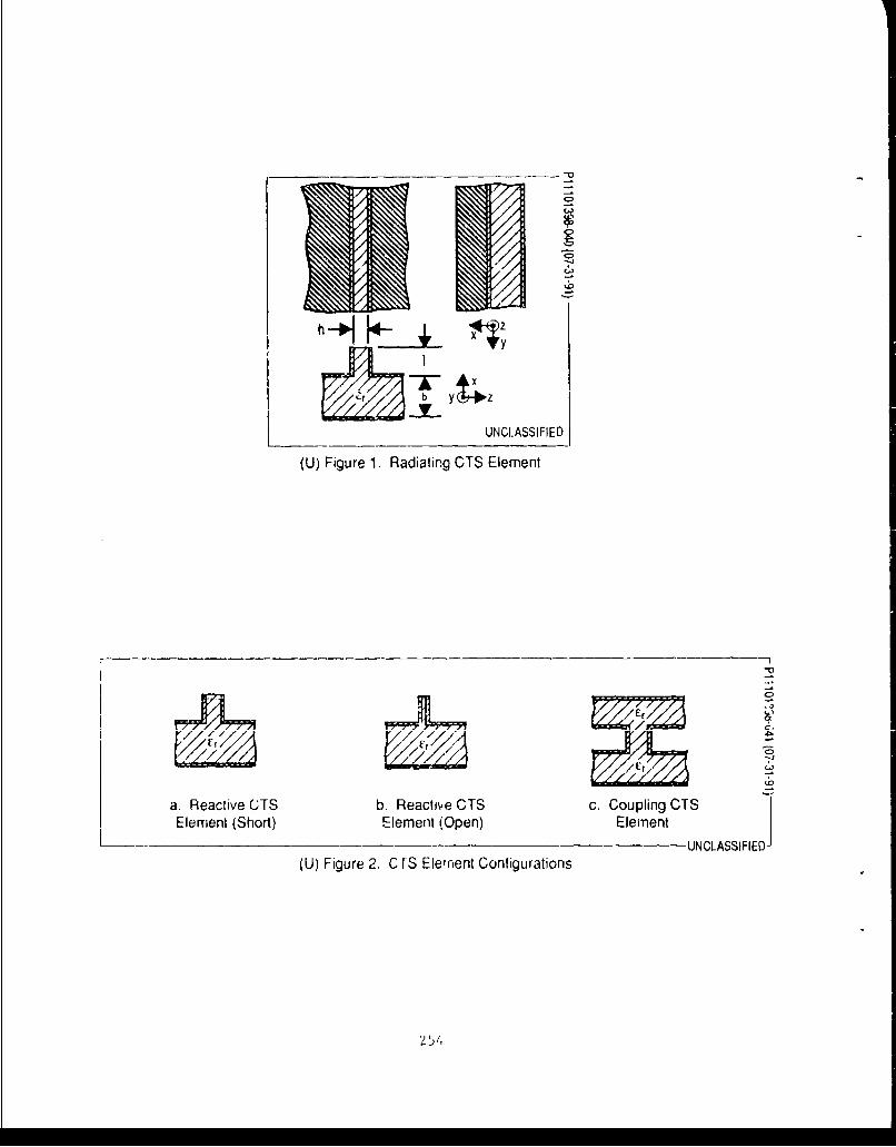
igure 1 illustrates the basic CTS element. Incident waveguide modes, launched via a primary line feed of
irbitrary configuration, have associated with them longitudinal electric current components which are
interrupted by the presence of a continuous or quasi-continuous transverse stub, thereby exciting a
LongitudinaL, z-directed displacement current across the stub/paratlel plate interface. This inryA'-ed
displacement current in turn excites equivalent x-traveling waveguide modes in the stub which travel to its
terminus and either radiate into freespace, are coupled to a second parallel oLate region, or are totally
reflected.
25 I 92-16057IIi Ii ii fli~l II~i I 'i hUI
"-c
C
Syf y
UNCLASSIFIED
(U) Figure 1. Radiating CTS Element
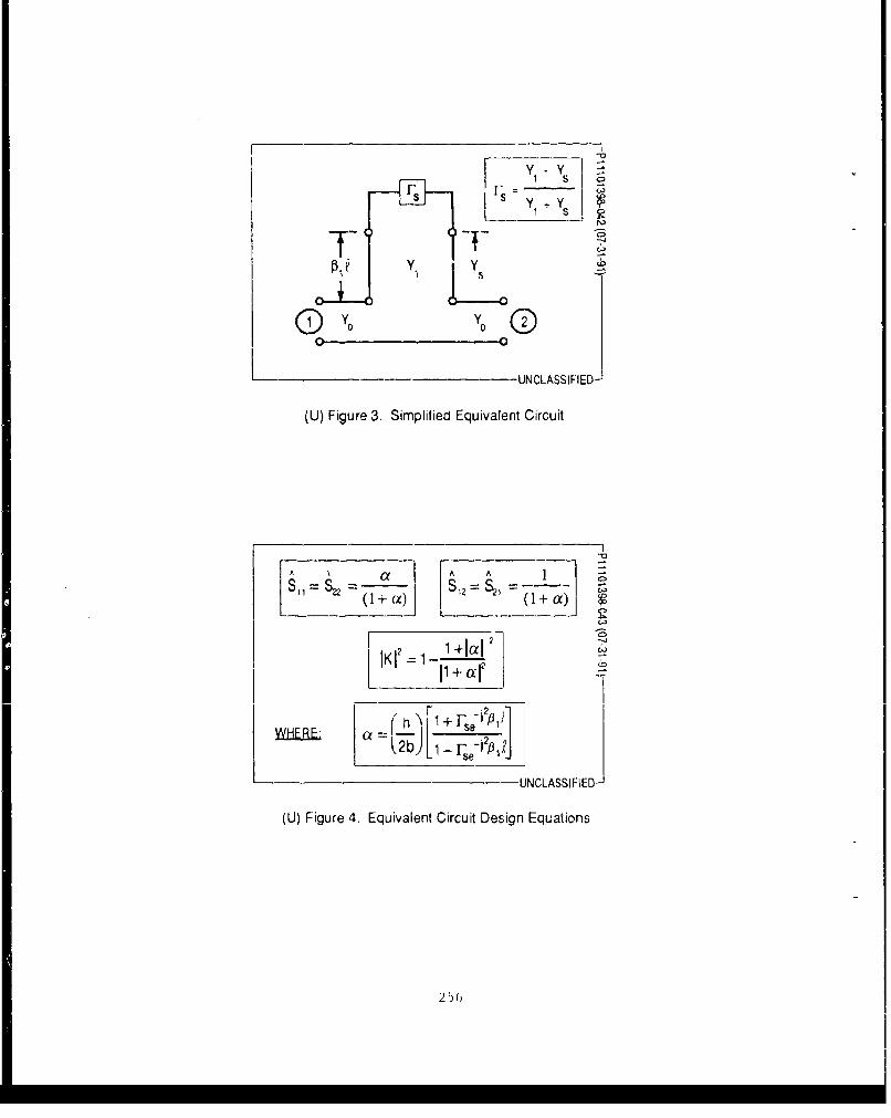
"a.
a. Reactive UTS b. Reactive CTS c. Coupling CTSElement (Short) Element (Open) Element
-UNCLASSIFIED
(U) Figure 2. C [S Element Configurations
254•/

For the radiator case, the electric field vector is linearly oriented transverse to the CTS element.
Radiating, coupling, or reactive CTS elements can be combined in a coomnon parallel plate structure to form a
variety of microwave, millimeter-wave, and quas.-optical components including integrated filters, couplers,
and antenna arrays. Figure 2 shows the basic CTS element in its short-circuit, open-circuit, and coupler
configurations.
Sackscattered energy from both the parallel plate/stub and stub/freespace or stub/secondary guide interfaces
:,herentLy interact with incident energy in the conventional transmission Line sense as shown in Figure 3.
these basic interactions are adequately m-deled and exploited using standard transmission line theory.
cringing effects at both interfaces are adequately modeled using conventional mode matching techniques and/or
-wo-dimensional finite element analysis. The variable length (1) and height (h) of the coupling stub controls
its electrical tine length (Bit) and characteristic admittance (Yj) and allows for controlled transformation
•f its terminal admittance (dependent primarily on h, er, and external mutual coupling effects) back to the
rain paraltcl plate transmission line, whose characteristic adiittance is governed by its height, b, thus
tllowing for a wide range of discrete coupling values, 1K1 2 from -3 Ae to less than -35 dB. Variations in
:oupLing stub length also allow for straightforward phase modulation of the coupled energy, as required in
Thaped beam antenna and multistage filter applications.
Figure 4 shows the derived scattering parameters (S 1 1 ,S 2 2 ,S 1 2 ,S 2 1 ) and coupling coefficient, 1K1 2, for the CTS
element based on simple transmission line theory (n-gtecting fringing effects.) Note that coupling values are
chiefly dependent on the mechanical ratio of stub height (h) relative to the height (b) of the parallel plate
waveguide region, consistent with a simple voltage divider relationship. Because this mechanical ratio is
independent of the operating frequency and dielectric constant of the structure, the CTS element is inherently
broadband and forgiving of small variations in mechanical and constituent material specifications. Ys may be
set to infinity, zero, or Y2 configurations without loss of generality. Note that the two-dimensional,
semi-infinite, non-resonant nature of the CTS structure lends itself well to relatively simple finite-element
and mode-matching analyses.
Based on the simple transmission-line model and assuming an isolated element, parameterized coupling curves
for radiating element coupling versus stub height (h) may be computed for the purpose of sensitivity analysis.
Figure 5 illustrates a nominal coupling curve (solid) for an element intended for operation at 60 GHz. Note
the benign effect of frequency, dielectric constant, stub height, and parallel-plate separation variation on
predicted coupling values (dash).
As an overmoded structure, the parallel plate transmission Line within which the CTS elements reside will
support a nuijber of waveguide modes which simultaneously meet the boundary conditions imposed by the two
conducting plates of the structure. The number and relative intensity of these propagating modes depends
255
1 S
1 S
N)
Y.YI"
UNCLASSIFIED-
(U) Figure 3. Simplified Equivalent Circuit
.71
A aA A1
11 22 ~~(1+ S1=2~la)
IK 12 1 - '
INHERL a (h'L 11 2
-- ~UNCLASSIFIED-
(U) Figure 4. Equivalent Circuit Design Equations
2')6

"-o
AS SUMPTIONS L-Fo = 60 Gliz _ _W0+_ _
Er =2.56 hb = 0.050 INCH hb = 0.028 INCHs = 0.132 INCH b '
= -, ~ ~NOMINAL """ -"
Z b 20% ,'.-IFo - 20%
S., /•/" (3.07)0
-25 -- i,
4 8 12 16 20 24 28
STRIP WIDTH IN MILS
UNCLASSIFIED
(U) Figure 5. Sensitivity Analysis of GIS Goupling Factor Versus Key Design Parameters
257

exclusively upon the transverse excitation function imposed by the finite line source. Once excited, these
mode coefficientr, are urnmodified by the presence of the CTS element because of its continuous nature in the
transverse plane.
In theory, each mode has associated jith it a unique propagation velocity which, given enough distance, will
cause undesirabte dispersive variation of the Line source imposed excitation function in the Longitudinal
direction of propc•gation. However, for typical excitation functions, these mode velocities differ from that of
the dominant TEN mode by much less than one percent and the transverse plane excitation imposed by the Line
source is therefore essentially translated, without modification, over the entire finite longitudinal extent
of the CTS array structure.
Figure 6 illustrates the theoretical constant wrplitude contours for the x-directed elc:ctric field within an
air filled 6 by 15 inch parallel plate region fed by a discrete dnear array located at y=O and radiating at a
frequency of 60 GHz. A cosine-squared amrplitude excitation wes chosen so as to excite a multitude of odd modes
within the parallel plate region. Note the consistency of the imposed transverse excitation over the entire
Longitudinal extent of the cavity.
The relative importance of edge effects ir the CTS array depends primarity on the impose i,ne source
excitation function, but they ere generally small because of the strict longitudinal dirertion of propagation
in the structure. In mny cases, especially those employing steep excitation tapirs, short circuits may be
int•oduced at the edge boundaries with Little effect on internal field distributions. In those applications
where edge effects are not negligible, load materials may be applied as required at the array edges.
3.0 Relative Advantage;
For antenna applications, a CTS array realized as a conductively plated dielectric has many performance,
producibility, and application advantages over conventional slotted waveguide array, printed patch array, Lnd
reflector/lens antenna approaches. Some distinct advantages in filter and coupler applications may be realized
as well.
The UTS technology is appLicable to all planar array applications at microwave, millimeter-wave, and
quasi-opt'cal frequencies. Shaped beams, multiple beams, dubl-polarization, dual-bends, and monoputse
functions Lan be accoeviodated. In addition, the planar CTS array is a prime candidate to replace reflector and
lens anter.nas in applications for which planar arrays have proved inappropriate because of traditional
bandwidth or cost limitations.

6.0-
I Fie Ame I I
(E 21 OveriParalle.Plate i
RegionI
4.5 I -
TEmr/TMmo -,
I1 I
30 -0 0.1967200"1 0.196724"Cy~ndr• O ng3 0.1967581"
Waver (Hanke) 5 0.19822Assumed for Each 7 0.1969276'Discrete Elmenit
1.5 /iII I , I I0.0
0.00 3.75 7.50 11.25 15.0iICcLASSIFIE0D
(U) Figure 6. Constant Amplitude Contours in CTS Parallel Plate Region
C.".,. i i i i , C...,1 •,- r ,- • i = / J •
-UNCLASSIFIED-- (U) a. Artificial Dielectric (U) b. Laminated DielectricCTS Element CTS Element
(U) Figure 7. Ai,-Filled CTS UNCLASSIFIED]Element
(U) Figure 8. Inhomogeneous Structures
259

Additional advantages in millimeter-wave and quasi-optical filter and coupler markets can be realized due to
the enhanced producibility and relative low loss of the CTS element over stripline, microstrip, and even
waveguide elements. FWter and coupler capabilities can be fully integrated with radiator functions in a
c•c•on structure.
Performance advantages include:
Superior aperture efficiency/enhanced fitter "1 "1 approximately one-half the loss of
dielectricalty-filted waveguide.
"Superior frequency bandwidth of up to one octave per axis, with no resonant components or structures.
"Superior broadband polarization purity, typically -50 dB cross-pot.
"Superior broadband element excitation range Rnd control, coupling values from -3 dB to -35 dB per
element ore realizable.
Superior broadband shaped-beam capability. Nonuniform excitation phase is implemented through modulation
of stub length and/or position.
Superior E-plane element factor. Recessed groundpiane allows for wide scanning capability, even to
endfire.
Superior power handling capability.
ProducibiLity advantages include:
Superlcr insensitivity to dimensional and material variations, b0.5U ft coupLing Vel ia•iun fur 20
percent change in dielectric constant, no resonant structures.
Totally externalized construction.
Sinplifted fabrication procedures and processes. Units can be thermoformed/extruded/injected in a single
mioding process, and no additional joining or assentbly is required.
Reduced design NRE costs and cycle time through modular/scalable design, simple and reliable RF
theory/analysis, and two-dimensional coiptexity which is reduced to one dimension.
200
Application advantages include:
Very thin profile.
Lightweight.
Conformal array can be curved without affecting internal coupling mechanisms.
Superior durability with no internal cavities.
"Oual-polarizaticn/dual-band/dual beam capable.
Frequency-scannable.
Electronically scannable.
Reduced radar cross section (RCS).
Applicable at millimeter-wave and quasi-optical frequencies.
Integrated filter/coupler/radiator functions in common structure.
4.0 CTS Element Variants and Applications
There are several variations on the basic CTS element that ray - useful in particular applications. They
are:
4.1 NondielectricalLy Loaded
A low density foam can be used as the transmission line mediurm for the CTS element as shown in Figure 7
to realize an efficient eleme.nt for an endfire array. The CTS radiator is particularly well-suited in
such applications due to its broad pseudo-uniform E-plane element pattern, even at endfire.
4.2 Slow-Wave/Inhomogeneous Structures
261

Figure Q shows that an artificial dielectric or multiple dielectric can be used in the parallel plate
-,Sion in applications for which minimal weight, compleA frequency dependence, or precise phase velocity
control is required.
4.3 Oblique Incidence
As shown in Figure 9, an oblique incidence of propagating waveguide modes can be achieved through
mechanical or electrical variation of the incoming phase front relative to the CTS radiator element axis
for scanning the beam in the transverse H-plane. This variation would normally be imposed through
mechanical or electrical variation of the primar! line feed exciting the parallel plate region. The
precise scan angle of this scanned beam will be related to the angle of incidence of the waveguide mode
phase front via Snelt's Law. That is, refraction will occur at the stub/freespace interface in such a
way as to magnify any scan angle imrposed by the mechanical or electrical variation of the line feed.
This phenomenon can be exploited to allow for relatively large antenna scan angles with only small
variations in line feed orientation/phasing. Coupling values can be expected to be pseudo-constant
(cosine-dependent) for small angles of incidence.
4.4 Longitudinal Incidence
A narrow CTS element will not couple dominant waveguide modes having phase fronts parallel to the stub
axis. This characteristic, shown in Figure 10, can be eAploited through implenentation of orthogonal CTS
radiator elements in a conieon parallel plate region. In this way, two isolated, orthogonally polarized
antenna modes can be simultaneously supported in a shiared aperture for the purpose of realizing
dual-polarization, dual-band, or dual-beam capabilities.
4.5 Parameter Variation in the Transverse Dimension
Stow variation of stub dimensions in the transverse dimension can be used to realize tapered coupling in
the transverse plane, as shown in Figure 11. This capability proves useful in antenna array applications
in which nonseparable aperture distributions are desirable or for nonrectangular array shapes. The
modified element is called a quasi-continuous transverse stub (OCTS.) Analysis results based on the
continuous transverse slot model can be expected to remain locally valid for the case of transverse
variation, assuming that variation profiles are smooth and gradual.
262

Coupled T
rI'r Sinej:Sin0r
-- UNCLASSIFIED--
(U) Figure 9. H-Plane Scanning Utilizing a Canted Phase-Front
Coupled T
7a
Isolated
-UNCLASSIFIED-
(U) Figure 10. Dual-Aperture Realization Utilizing CTSElements
263

Decreased Coupling
Increased Coupling
_____________________________ -- UNCLASSIFIED-(U) Figure 11. Quasi-Continuous Transverse Stub (OCTS)
- - -- - - -- -
/a
0//

4.6 Finite width Element
Although conventionally very wide in the transverse extent, the CTS element can be utilized in reduced
width configurations down to and including simrpLe rectangular waveguide. The sidei.ails of such a
truncated CTS element, shown in Figure 12, may be terminated in short circuits, open circuits, or Loads
as dictated by the particular application.
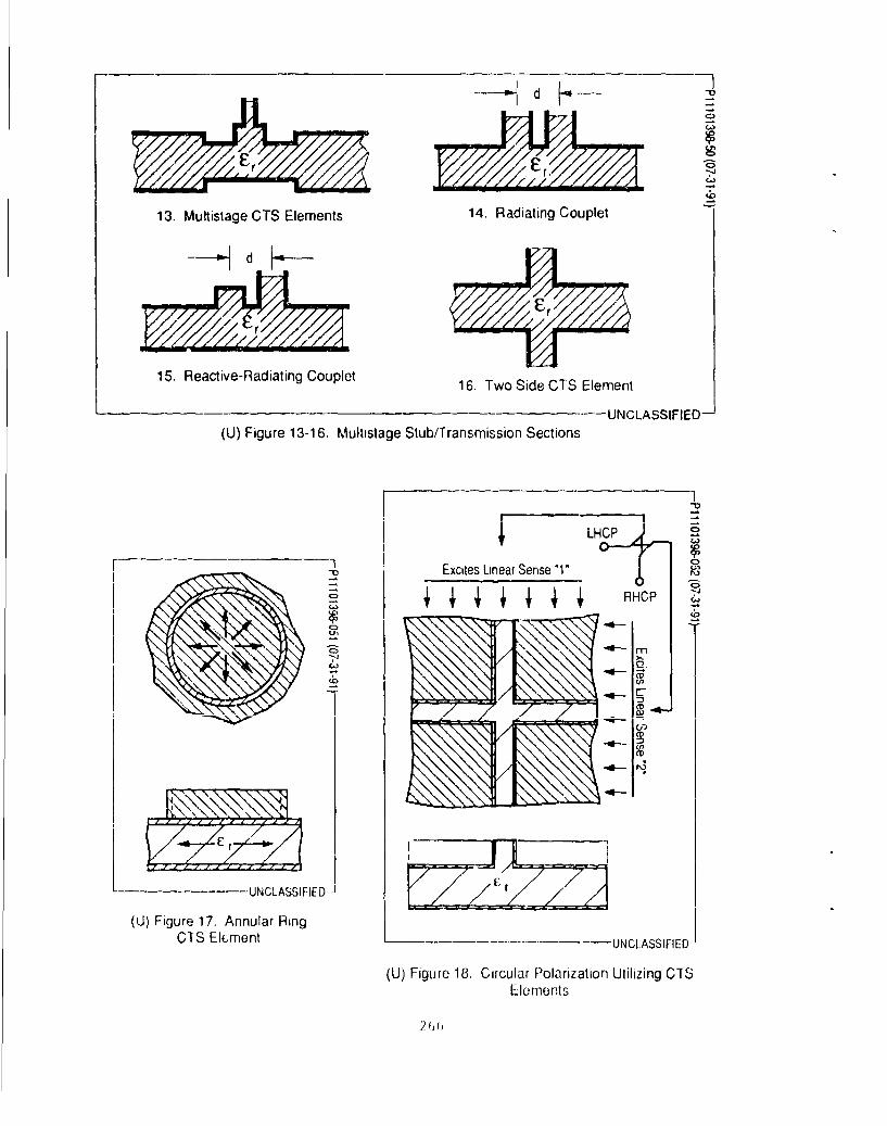
4.7 Multistage .tub/Transmission Sections
Figure 13 shows that multiple stages can be employed in the stub or parallel plate regions to modify
coupling or broaden frequency bandwidth characteristics of the structure as dictated by specific
electrical and mechanical constraints.
4.8 Paired Elements (Matched Couplet)
Figure 14 shows how pairs of closely spaced similar CTS radiator elements can be used to customize
composite antenna element factors or to minimize composite element VSWR through destructive interference
of individual reflection contributions. Bandpass filter implementations can also be realized in a
similar fashion when purely reactive CTS elements are used.
4.9 Radiating/Nonradiating Stub Pairs (Matched Couplet)
Figure 15 shows how a nonradiating purely reactive CTS element can be paired with a CTS radiator element
to suppress coupler/radiator reflections through destructive interference of individual reflection
contributions, resulting in a matched CTS couplet element. Such couplet elernwnt6 may prove particularly
useful in CTS array antennas when scanning the beam at or through broadside is required.
4.10 Double Sided Radiator/Filter
Figure 16 shows how radiator, coupler, and/or reactive stubs can be realized on both sides of the
parallel plate structure to economize space or for antenna applications in which radiation from both
sides of the parallel plate is desirable.
4.11 Radial Applications
The CTS element can be utilized in applications in which cylindrical waveguide modes are used in place
of plane waveyuide modes. As shown in Figure 17, the CTS element forms closed concentric rings in this
265
--- Ad ~--
o
13. Multistage CTS Elements 14. Radiating Couplet
-d K
15. Reactive-Radiating Couplet 16. Two Side CTS Element
-UNCLASSIFIED-
(U) Figure 13-16. Multistage Stub/Transmission Sections
-v Excites Linear Sense 1"0-T
o ~RHOP 2
CD
-- *4
U-- ---- UNCLASSIFIFED 1
(U) Figure 17. Annular RingCTS Elcment -UNCLASSIFIED
(U) Figure 18. Circular Polarization Utilizing CTS
Elements
2GbO

radial configuration with coupling mechanisms and characteristics similar to those for the ptar~e wr-ve
case. Single or multiple point sources serve as a primary feed. Both radiating and nonradiating versions
of the CTS element can be realized for the cylindrical case. Such arrays may be particularly useful for
antennas requiring high gain 360 degree coverage oriented along the radial direction and in one-port
filtet applications.
4,12 Circ-itar Polarization
Although the CTS radiator element is exclusively a Linearly polarized antenna element, Figure 18 shows
how circular polarization can be realized in a straightforward fashion either through a standard
quarter-wave plate polarizer or through quadrature coupling of orthogonally oriented CTS radiator
elements or arrays.
5.0 Array Variants and Applications
The CTS element can be combined or arrayed to form a planar structure fed by an arbitrary line source. This
line source may be either a discrete linear array, such as a slotted waveguidz, or a continuous linear source,
such as a pitt-box or sectoral horn. Two Line sources are used in filter and coupler applications to form a
two-port device. Irt the case of antenna applications, a single line feed is utilized to impose the desired
aperture distribution in the transverse plane white the parameters of individual CTS radiator elements are
varied to control the aperture distribution in the longitudinal plane.
In fitter and coupler applications, a second line feed can be introduced to form a two-port device comprised
of CTS coupler or reactive elements. For antenna applications, either a short circuit, open circuit, or load
can be placed at end of the CTS array opposite the line source to form a conventional standing wave or
traveling wave feed.
Standaid array, coupler, and filter synthesis and analysis techniques can be used in the selection of
interelement spacings and electrical parameters for individual CTS elements in CTS array specifications.
Normalized design curves relating the physical attributes of the CTS element to electrical parameters are
derived either analytically or --mpirically to realize the desired CTS array characteristics.
The simple modutlr design of tne CTS array greatly reduces the design NRE costs and cycle time associated with
conventional planar arrays. Typical planar array developments require the individual specification and
fabrication of each discrete radiating element along with associated feed components such as angle slots,
input slots, 3nd corporate feed. In ;ontrast, the CTS planar atrray requires the specification of only two
267

linear feeds, one comprised of the array of CTS elements, the other of the requisite line feed. These feeds
c€- be designed and modified separately and concurrently and are fully specified by a miininiui nurber of unique
parameters. Drawing counts and drawing comrplexities are thus reduced. Design modification: or iterations are
easily and quiikly implemented.
5.1 Pencil Beam Array
A standard pencil beam antenna array as shown in Figure 19 can be constructed using the CTS array
concept with principle plane excitations implemented through appropriate selection of Line source and
CTS element parameters. Element spacings are conventionally chosen to be approximately equal to an
integral rnumer of wavelengths within the parallel plate region. Ionoputse functions can be realized
through appropriate modularization and feeding of the CIS array aperture
5.2 Shaped Beam Array
The variable length of the stub portion of the CTS radiator allows for convenient and precise control of
individual element phases in CTS antenna array applications. This control, in conjunction with the CIS
element's conventional capability fur discrete amplitude variationi, allows fui pie~ise spcificati :. ý,d
realization of complex shaped beam antenna patterns, as shown in Figure 20. Examples include
cosecant-squared and nonsymmetric sideLobe applications.
5.3 Multi-Aperture Array
The continuous stubs of a CTS array typically occupy no more than 10 to 20 percent of the total planar
antenna aperture or filter area. The radiating apertures of these stubs are at their termination and are
therefore raised above the groundplane formed by the main parallel plate transmission line structure.
Relatively wide, continuous, transverse, conductive troughs are therefore formed between individual CT$
elements as shown in Figure 21. These troughs can be exploited to introduce secondary array structures.
Possible exploitations include closing the trough to form a slotted waveguide cavity as shown in Figure
22; interdigitation of a printed patch array; slotting of the trough region to couple alternative modes
from the parallel plate transmission line; or introduction of active elements as adjuncts to the CIS
array structure.

I0n i
.+ 4- -6 11- t n+i C5
(U) 19. Pencil Beam Antenna Array (U) 20. Shaped Beam Array
"Trough" iTansverse WIG
(U) 21. CTS Element Trough (U) 22. Slotted Waveguide CavityUNCLASSIFIED
(U) Figure 19-22. CTS Array Applications
269
5.4 Dual Polarization Array
An identical pair of orthogonally oriented CTS arrays can be utilized as shown in Figure 23 to realize a
dual-polarization planar array sharing a common aperture area. Circular or elliptical polarizations can
be realized through appropriate combination of the two orthogonal signals via a fixed or variable
quadrature coupler or with the introduction of a conventional Linear-to-circular polarizer. The pure
linear polarization of individual CTS radiating elements and the natural orthogonality of the parallel
plate waveguide modes provides this approach with superior broadband polarization isolation.
5.5 Duat-Beam Array
in a manner similar to the duel polarization approach, two dissimilar orthogonally oriented CTS arrays
can be employed to provide a simultaneous duat antenna beam capability. ?or example, one CTS array might
provide a vertically polarized pencil beam for air-to-air raoar modes while another provides a
horizontally polarized cosecant-squared beam for ground mapping. Dual squinted pencil beams for
microwave relay represents a second application of this dual beam capability.
5.6 Dual-Barnd Array
Again utilizing a pair of orthogonally orientec CT5 arrays, a dual-band planar array can be constructed
through appropriate selection of interelement spacings and CTS element parameters for each array. The
two selected frequency bands can be widely separated due to the dispersionless nature of the parallel
plate transmission line structure and the frequency independent orthogonality of the waveguide modes.
5.7 Dual Guided Mode Array
Pericdicalty spaced slots can be introduced in the trough regions between individual CTS array elements
to couple alternative mode setz from the parallel plate transmission line structure. For exampLe, a TE
mode whose electric field vector is oriented parallel to the conducting plates of the parallel plate
transmission line may be seLectively coupled through the introduction of thick or thin in.lined slots in
the interel•ement trough regions, as shown in Figure 24. These slots may protrude slightly from the
conductive plate groundplarie to aid in fabrication. Such a mode is not coupled by the CTS elements due
to the transverse orientation of its induced watt currents and the cut-off conditions of the CTS StLUbS.
Li'ewise, the waveguide modes of the parallel plate waveguide structure, with its etectric field vector
oriented perpendicular to the conducting plates of the parallel plate transmission line, are not coupled
to tht inclined slots due to the disparity in operating and slot resonant frequencies, particularly for
thick stlots. In this way a dual-band planar array is formed with frequency band offsets regulated by the
270

Line Feed #2 J
R R O M P R I UNCI ASSIFIEDI
(U) Figure 23. Dual Polarization Array
271

Wv
C)
9 (E-Lines)
4'-(E-Lnes)
(U) 24. Interelement Trough Regions (U) 25. Electric FiEld Components
-- UNCLASSIFIED]
(U) Figure 24-25. Multimode Capabilities
M/
intereLement spacing of the CTS and inclined slot elements and the parallel plate spacing of the
parallel plate transmission line.
Figure 25 shows the electric field compionents for TEM and TE0 1 modes. Dual-beam and dual-polarization
apertures may also be realized using intentional multimode operation.
5.8 Fixed or Variable H-Plane Beam-Squint Array
As shown in Figure 26, an intentional fixed or variable beam squint (in one or both planes) can be
realized with a CTS array through appropriate selection of CTS array element spacing, constituent
material dielectric Lonstant, or requisite line feed characteristics. Such a squinted array may be
desirable for applications in which mounting constraints require deviation between the mechanical and
electrical boresights of the antenna.
5.9 H-Plane Scanning by Mechanical Ditnering of Line-Feed
The requisite line feed for a CTS antenna array can be mechanically dithered to vary the angle of
incidence, or phase slope, of the propagating parallel plate waveguide moides relative to the CTS element
axis. In doing so, a refraction enhanced beam squint of the antenna bcam is realized in the transverse
H-plane of the array, as shown in Figure 27.
5.10 H-Plane Scanning by Electrical Variation of Line-Feed Propagation Constant
Figure 28 shows an alternate method of varying of the angle of incidence of the propagating parallel
plate waveguide modes relative to the CTS element axis. Such varlet.on cat'ses squinting of the phase
front emanating from the line source while maintaining a fixed, parallel, mechanical orientation
relative to the CTS element axis.
5.11 E-Plane Scanning by Variation of Planar Propagation Constant
Variation of the phase velocity within the parallel plate transmission tine structure will scan the beam
in the longitudinal E-plane. Such a variation may be induced through appropriate electrical or
mechanical modulation of the constituent properties of the dielectric material contained within the
parallel plate region. This scanning technique can be comtbined with scanning techniques in the
transverse plane to achieve simultaneous beam scanning in two dimensions. This is the basic Hughes
approach for eyploiting voltage-controlled dielectric materials.
273

-C,
-il
S. .. . .. UNCLASSIFIED - UNCLASSIFIED,
(U) Figure 26. Squint Beam Array (U) Figure 27. Mechanical Line Feed Scanning
.74
EE
UUNCLASSIFIE UD 1
(U) Figure 28. Line Feed Phase Velocity (U) Figure 29. Frequency Scanning
Variation Scanning
274
This modulation in phase velocity within the parallel plate transmission line structure can also be used
in CTS array filter and coupler structures to frequency tune their respective passbands or stopband
responses.
5.12 E-Plane Frequency Scanning
As shown in Figure 29, when used as r traveling wave antenna array structure, the position of the
antenna mainbeam will vary with irequency. In applications where this phencmenon is desirable,
interelement spacings and material dielectric constant values can be chosen to enhance this frequency
dependent effect. For example, a CTS array fabricated from a high dielectric material (er =12) will
exhibit approximately a two degree beam scan for a one percent variation in operating frequency.
5.13 Conformal Array
The absence of internal details within the CTS structure allows for convenient deformation of its shape
to conform to curved mounting surfaces, e.g., wing leading edges, missile/aircraft fuselages and
automobile bodywork. As shown in Figure 30, the overmoded nature of the CTS structure allows such
deformation to large radii of curvature without perturbation of its planar coupling characteristics.
The interelement trough regions in the CTS array structure can provide a means for suppression of
undesirable surface wave phenomena normally associated with conformal arrays. Deformation of the
radiated phase front emanating from such a curved CTS array may be corrected to planar through
appropriate selection of line feed and individual CTS element radiator phase values.
5.14 End-fire Array
The CTS array can be optimized for endfire operation, as shown in Figure 31, through appropriate
selection of interetement spacings and constituent material characteristics. The elevated location
relative to the interstub groundplane of the individual CTS radiator element surfaces affords a broad
element factor and yields a distinct advantage to the CTS element in endfire applications.
5.15 Non-Rectangular Apertures
As shown in Figure 32, variation of CTS element parameters in the transverse plane yields a
quasi-continuous transverse stub (QCTS) element that can be used in OCTS arrays for which nonseparable
aperture distributions or nonrectanguLar aperture shapes (circular or elliptical) are desired. For
continuous, smoothly varying modulation of OCTS element parameters, the excitation, propagation, and
275

...... f ~ 2RadiatorA A SurfaceI I Elevated
-*J -~ AboveoGround- 8,
- ~~~UNCLASSIFIED]1 UCASIID(U) Figure 30. Conformal Array (U) Figure 31 . Endt ire. Array
UNCLASSIFIED -UCASIID(U) Figure 32. Nonseparable Shaped Array (U) Figure 33. Radial Array
jy yiyo -
-~ ~~~ _-UCLSI0 E
(U)~~~~~U Fiur 34. CTS Filters()b qialnici
270

coupling of higher order modes within the QCTS array structure can be essu•med to be locally similar to
that of the standard CTS array and hence the CTS array design equations can be applied Locally across
the transverse plane in QCTS applications.
5.16 RCS Characteristics
The absence of variation in the transverse plane for CTS arrays eliminates scattering contributions
(Bragg lobes) which would otherwise be present in traditional two-dimensional arrays comprised of
discrete radiating elements. in addition, the dielectric Loading in the crS array allows for tighter
interelement spacing in the longitudinal plane and therefore provides e means for suppression or
manipulation of Bragg Lobes in this plane. The capability to intentionally squint the mainbeam in CTS
array applications also affords it an additional design advantage in RCS performance.
5.17 Radial cTS Arrays
As shown in Figure 33, the CTS array can also be realized in radial form, in which case the continuous
transverse stubs form continuous concentric rings. A single or a multifmfode point source replaces the
traditional line source in such applications. Radial wavwguide modes are used in a similar manner to
plane waveguide modes to derive design equations for the radial CTS array.
Dual-polarization, dual-band, and dual-beam capabilities can be realized with the radial CTS array
through appropriate selection of feeds, CTS element, and auxiliary element characteristics in a manner
directly parallel to that for the planar CTS array. Similar performance, application, and producibilitý
advantages apply. Both endfire and broadside mainbeam patterns can be realized with the radial CTS
array.
5.18 Filters
As shown in Figure 34, nonradiating reactive CTS elements terminated in an open or short circuit can be
arrayed to conveniently form fiLter structures. Such structures can function independently as filters or
be coebined with radiating elements to fvrm an integrated filter/multiptlexer/antenna structure.
Coirtcntionat methods of filter analysis and synthesis may be cmployed with the CTS array fitter without
loss of generality.
The CTS array enjoys advantages over conventionaL filter realizations, particularly at millimeter-wave
and quasi-optical frequencieG where its diminished dissipative losses and reduced mechanical tolerance
siensitivities allow for the efficient tabrication of high precision, high "O0 devices. No-e that the277

theoretical dissipative losses for the CTS array parallel plate transmission line structure are
approximately one-half of those associated with a standard rectenguler waveguide operating at the
identical frequency arn comprised of identical dielectric and conductive materials.
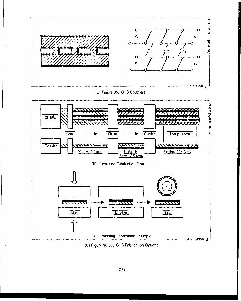
5.19 Coup(lrs
As well as for filters as shown in Figure 35, precision couplers may also be realized and integrated
using the CTS array structure with individual CTS elements functioning as branch guide surrogates.
Again, conventional methods of coupler analysis ond synthesis can be used without loss of generality.
6.0 Fabrication Methods
Fabrication of the dielectrically loaded CTS element can be efficiently accomplished through machining or
molding of the dielectric structure, followed by uniform conductive plating to form the parallel plate
transmission line, and finally, in the case of antenna applications, machining or grinding of the stub
terminus to expose the stub radiator.
Mature fabrication technologies such as extrusion, injection molding, and thermomolding are ideally suited to
the fabrication of CIS arrays. in many cases the entire CIS array, including all feed details, can be formed
in a single exterior molding operation.
A typical three step fabrication cycle includes structure formation by continuous extrusion or closed single
step molding; uniform exterior metalizetion by plating, painting, lamination, o deposition; and planar
grinding to expose input, output, and rad;ating surfaces. Due to the absence u, interior details, the CIS
array requires metalization on exterior surfaces only witn no stringent requirement for metalization
thickness, uniformity, or masking.
Figure 36 shows a typical continuoub extrusion process whereby the stubs of the CTS array structure are
formed, metelized, and trimmed in a continuous sequential operation. Such an operation results in long CTS
array sheets which may subsequently be diced to form individual CIS array structures. Figure 37 depicts a
similar discrete process by which individual CTS array structures are molded or formed, metalized, and trimmed
in a sequence of discrete operations.
The relative insensitivity of the nonresonant CTS element to dimensional and materlw, variations greatly
enhanices its producibility over concpeting resonant approaches. This, in conjunction with the relative
simplicity of the oesign and fabrication of the CTS array, makes it an ideal candidate for tow cost high
procluction rate applications. 278
-v
YO YO
- -- -- ---- - -UNCLASSIFIEDJ
(U) Figure 35. CTS Couplers
-5
Form ---- Plating --- * Grinder Trim 10 Lenqth
ExtruderSZSS SS4S
Elte I5Ar&ray
36. Extrusion Fabrication Example
r
Mold M etalizeGrn
37. Pressing rabrication Example - - UNLSIED
(U) Figure 36-37. CTS Fabrication Options
279
T.O Specific Actication Exairces
As a initial effort, a small CTS antenna array was fabricated to demonstrate the CTS element and array
concepts for antenna applications. Coarse approximations for coupling and radiating characteristics were used
in lieu of precise analytical models and emipirical design data. This teut piece was thus a feasibility
demonstration and not an optimized design.
A 6.0 by 10.5-inch CTS antenna array was fabricated from rexolite (er=2
.3
5, ltan=0.0003). This array was
coeprised of 20 CTS radiator elements and designed for operation in the 12.5 to 18 GHz frequency band. A
moderate amplitude excitation taper was imposed in the longitudinal plane through appropriate variation of CTS
stub widths having constant individual heights. Interetement spacing was 0.500 inch and parallel plate spacing
was 0.150 inch. A silver based paint provided a uniform conductive coating over alt exposed areas of the CTS
array. Input and stub radiator surfaces were exposed after plating using a mild abrasive.
An H-plane sectorat horn, 0.1p by 6 inches, was designed and fabricated as a simple Low cost Ku-band line
source, providing a cosinuscidal amptitude and a 90 degree peak-to-peak parabolic phase distribution at the
input of the CTS array. A quarter-wave transformer was built into the CTS array to match the interface between
it and the sectorat horn Line source.
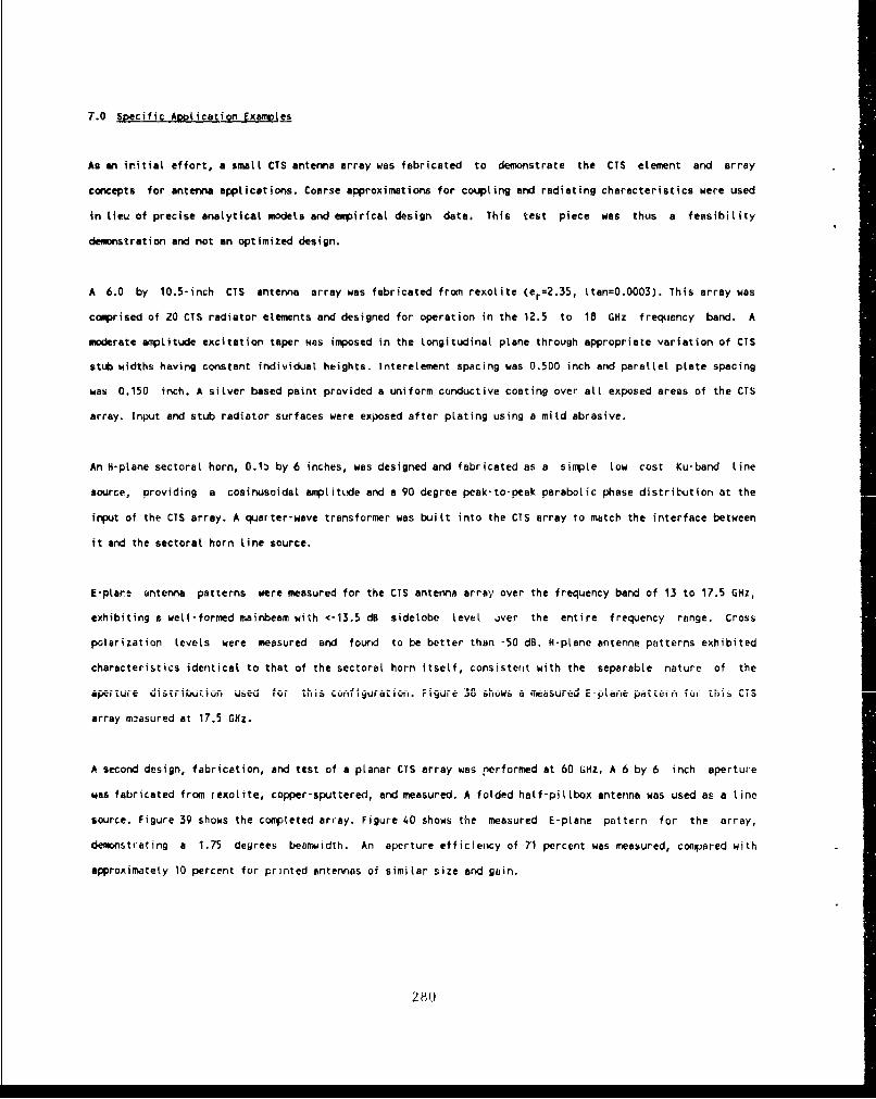
E-ptare antenna patterns were measured for the CTS antenna array over the frequency band of 13 to 17.5 GHz,
exhibiting a welt-formed mainbeam with <-13.5 dB sidelobe level 4ver the entire frequency range. Cross
polarization Levels were measured and found to be better than -50 dB. H-plane antenna patterns exhibited
characteristics identical to that of the sectorat horn itself, consistent with the separable nature of the
aperture d i'stiior, used for this con~figuration1. Fgurýue 30 shows a measured E-pLare pattewn lo, this CTS
array maasured at 17.5 GHz.
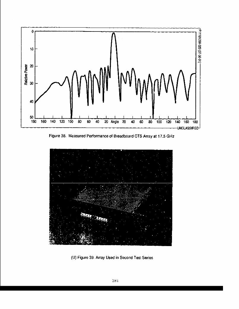
A second design, fabrication, and test of a planar CTS array was nerformed at 60 GHz, A 6 by 6 inch aperture
was fabricated from rexotite, copper-sputtered, and measured. A folded hatf-piLlbox antenna was used as a line
source. Figure 39 shows the completed array. Figure 40 shows the measured E-pLane pattern for the array,
deonrstrating a 1.75 degrees beamwidth. An aperture efficiency of 71 percent was measured, compared with
approximately 10 percent for printed antennas of similar size and gain.
280
0 -16
10-
~20
cc 30
40
50 L - I -
180 160 140 120 100 80 60 40 20 Arigle 20 40 60 80 100 120 140 160 180
UNCLASSIFIED
Figure 38. Measured Performance of Breadboard CTS Array at 17.5 GHz
(U) Figure 39. Array Used in Second Test Series
281

8W3 1.750
10
~20
30
180 160 140 120 100 80 60 40 20 Angle 20 40 60 80 100 120 140N160•180
UNCLASSIFIED-(U) Figure 40. Measured Performance of Millimeter-Wave CTS Array at 60 GHz
Figure 41. Dual-Polarization CTS Array (Ku-Band)
282

8.0 Continuing and Future Development
Current ongoing developments of the CTS antenna array include fixed and one-dimensional scanning applications
at 12, 33-50, 35, and 94 GHz. These applications include both single and dual polarization realizations for
the military, automotive, commerical avionics, and consumer marketplaces. As an example, Figure 41 depicts a
prototype dual-polarization Ku-band CTS array currently under development as a tow-cost planar antenna for the
Direct Broadcast Satellite (DBS) consumer market. Applications of dual-band, two-dimensional scanning, and
conformal capabilities have been formally proposed.
Analytical developments underway include improved equivalent circuit, mode-matching and finite-element models
in order to more rigorously account for mutuaL-coupling, fringing, and dissipative toss effects. Analysis of
inhomogeneous, time-varying, and anisotropic dielectric materials and CTS geometries have been proposed.
283