combinational circuits: multiplexers, decoders ...staff.cs.upt.ro/~todinca/dl/lectures/muxes.pdf ·...
TRANSCRIPT
Combinational Circuits:
Multiplexers, Decoders,
Programmable Logic Devices
Lecture 5
Doru Todinca
Textbook
• This chapter is based on the book [RothKinney]:
Charles H. Roth, Larry L. Kinney, Fundamentals
of Logic Design, Sixth Edition, Cengage
Learning. 2010
• Figures, tables and text are taken from this
book, Unit 9, Multiplexers, Decoders, and
Programmable Logic Devices, if not stated
otherwise
• Figure numbers are those from [RothKinney]
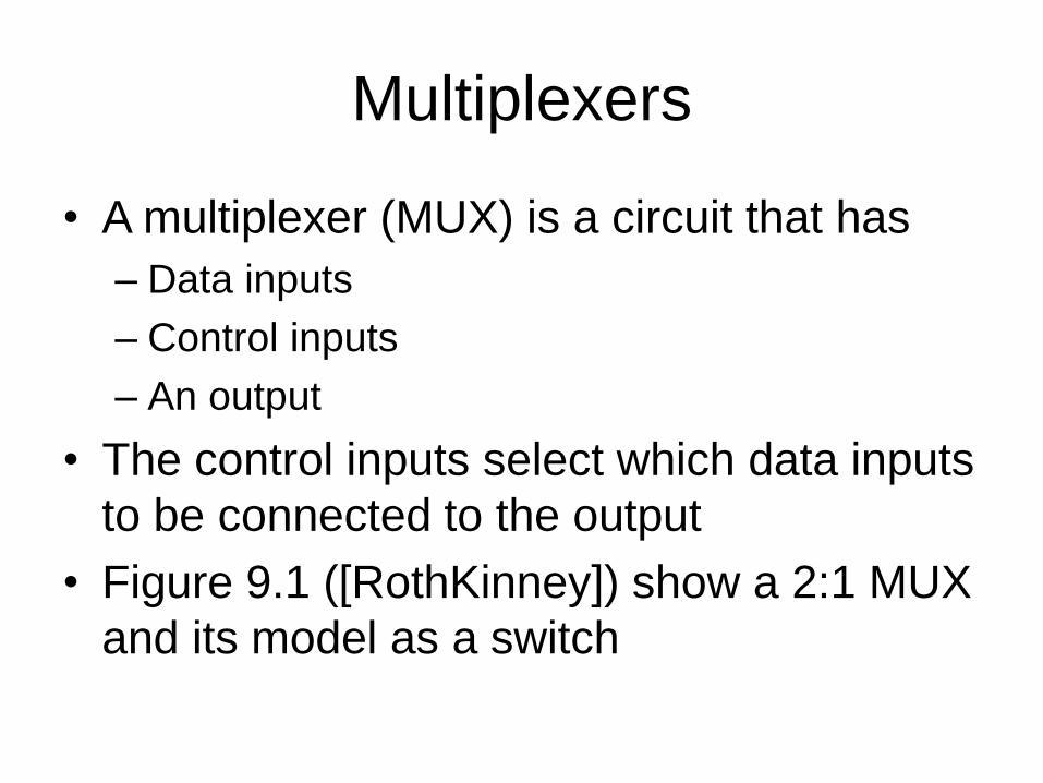
Multiplexers
• A multiplexer (MUX) is a circuit that has
– Data inputs
– Control inputs
– An output
• The control inputs select which data inputs
to be connected to the output
• Figure 9.1 ([RothKinney]) show a 2:1 MUX
and its model as a switch
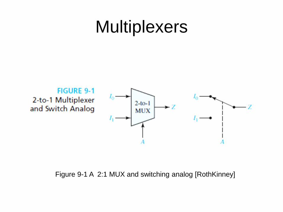
Multiplexers
Figure 9-1 A 2:1 MUX and switching analog [RothKinney]
Multiplexers
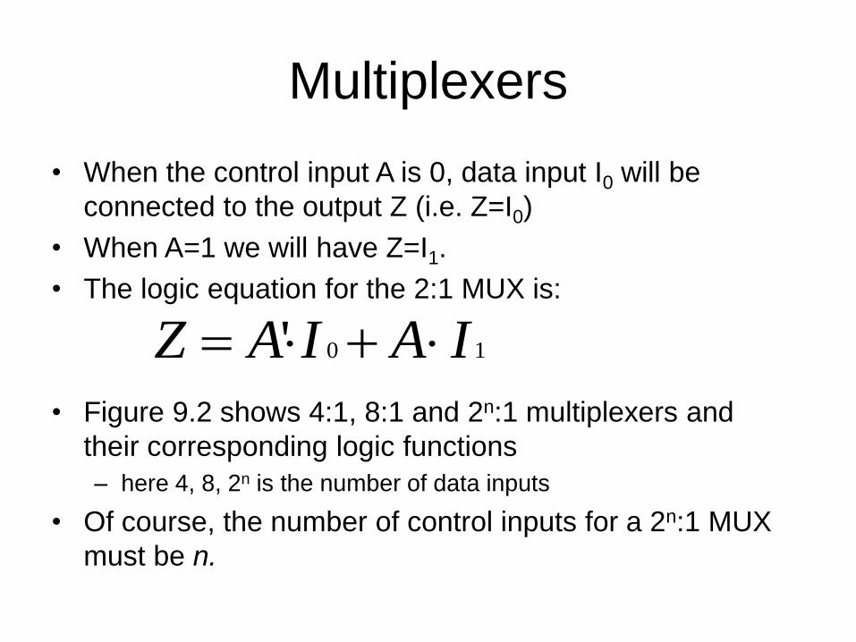
• When the control input A is 0, data input I0 will be
connected to the output Z (i.e. Z=I0)
• When A=1 we will have Z=I1.
• The logic equation for the 2:1 MUX is:
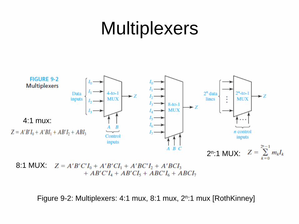
• Figure 9.2 shows 4:1, 8:1 and 2n:1 multiplexers and
their corresponding logic functions
– here 4, 8, 2n is the number of data inputs
• Of course, the number of control inputs for a 2n:1 MUX
must be n.
10' IAIAZ
Multiplexers
4:1 mux:
8:1 MUX:
2n:1 MUX:
Figure 9-2: Multiplexers: 4:1 mux, 8:1 mux, 2n:1 mux [RothKinney]
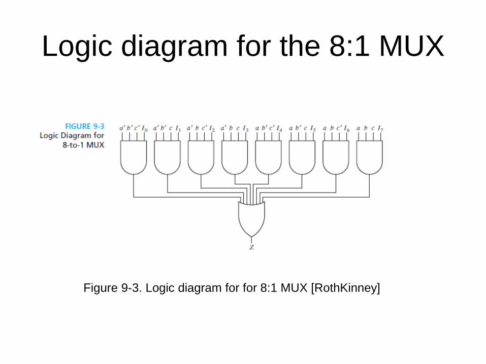
Logic diagram for the 8:1 MUX
Figure 9-3. Logic diagram for for 8:1 MUX [RothKinney]
Example of MUX application
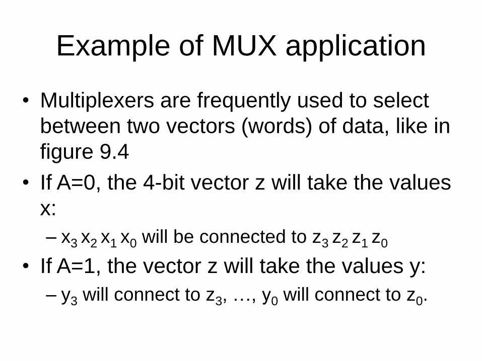
• Multiplexers are frequently used to select
between two vectors (words) of data, like in
figure 9.4
• If A=0, the 4-bit vector z will take the values
x:
– x3 x2 x1 x0 will be connected to z3 z2 z1 z0
• If A=1, the vector z will take the values y:
– y3 will connect to z3, …, y0 will connect to z0.
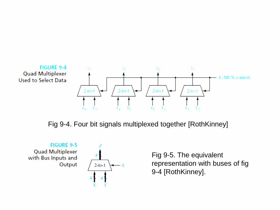
Fig 9-5. The equivalent
representation with buses of fig
9-4 [RothKinney].
Fig 9-4. Four bit signals multiplexed together [RothKinney]
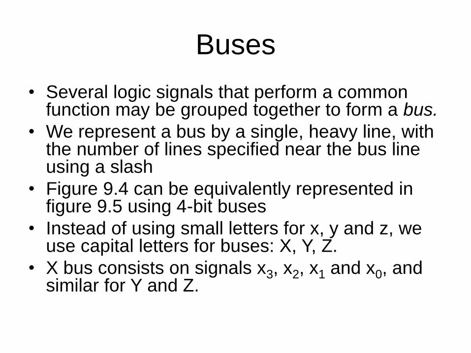
Buses
• Several logic signals that perform a common function may be grouped together to form a bus.
• We represent a bus by a single, heavy line, with the number of lines specified near the bus line using a slash
• Figure 9.4 can be equivalently represented in figure 9.5 using 4-bit buses
• Instead of using small letters for x, y and z, we use capital letters for buses: X, Y, Z.
• X bus consists on signals x3, x2, x1 and x0, and similar for Y and Z.
Enable inputs
• The multiplexers can have the outputs active high (like in previous figures), or active low.
• If a signal is active low, we use an inverting bubble on the circuit diagram, for that signal
• A multiplexer, like many other circuits, can have additional enable inputs:– When the enable input is active, the circuit (mux in
this case) works normally
– When the enable input has the inactive value, the circuit’s outputs are all inactive: all 0 if they are active high, all 1 if they are all active low, or all in high-impedance (see later tri-state buffers).
Buffers
• The number of circuit inputs that can be driven
by a single output is limited
• If a circuit output must drive many inputs, we use
buffers to increase the driving capability
• In figure 9.6 the buffer (having the output F) is a
noninverting buffer: it does not perform any logic
function, i.e. its logic equation is F=C.
• It only increases the driving capability
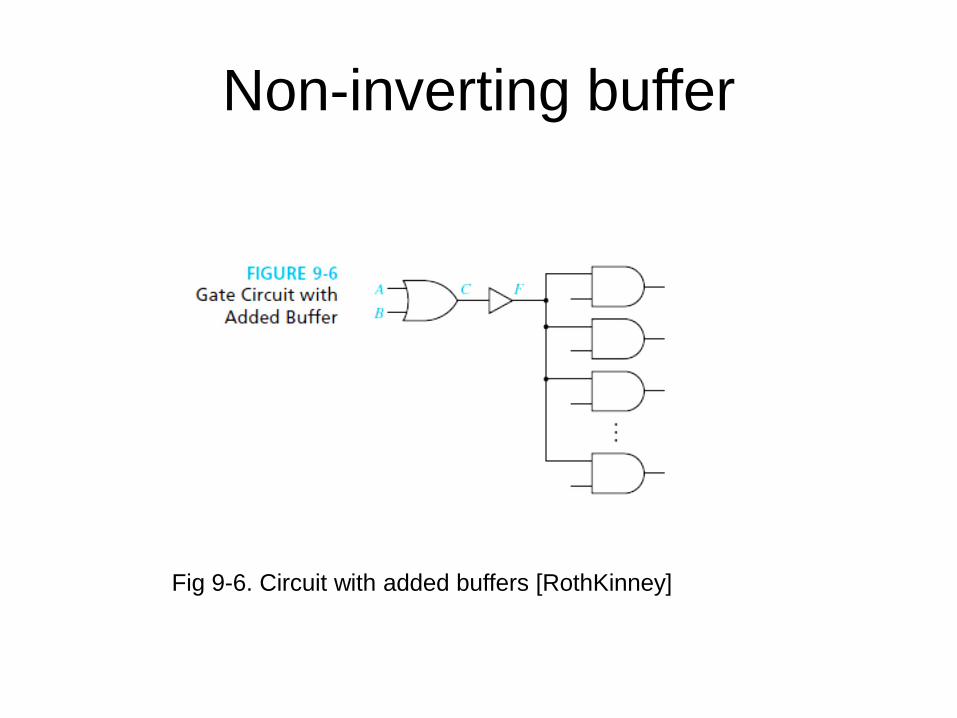
Non-inverting buffer
Fig 9-6. Circuit with added buffers [RothKinney]
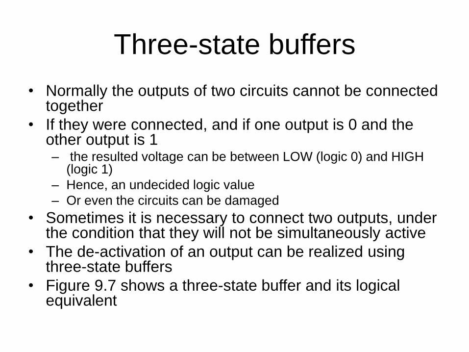
Three-state buffers
• Normally the outputs of two circuits cannot be connected together
• If they were connected, and if one output is 0 and the other output is 1– the resulted voltage can be between LOW (logic 0) and HIGH
(logic 1)
– Hence, an undecided logic value
– Or even the circuits can be damaged
• Sometimes it is necessary to connect two outputs, under the condition that they will not be simultaneously active
• The de-activation of an output can be realized using three-state buffers
• Figure 9.7 shows a three-state buffer and its logical equivalent
Three-state buffers
• Normally, there is a path between the output of a circuit and – either GND (ground) => Vout=LOW, or VCC (+5V) => Vout=HIGH
• There are circuits (buffers) for which the paths to GND and VCC are both blocked
• The output of the buffer is then in a high-impedance state, called Hi-Z (the third state)
• No current can flow in the buffer’s output, the buffer has a very high resistance (impedance)
• Logically, it is as if the output of the buffer is disconnected (see figure 9.7)
• Three-state buffers are called also tri-state buffers
• The three state buffers have an enable input (B in figure 9.8) that determines if the buffer functions as a normal buffer, or its output is in Hi-Z
• The command and the output can be inverting or non-inverting
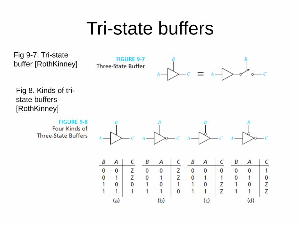
Tri-state buffers
Fig 9-7. Tri-state
buffer [RothKinney]
Fig 8. Kinds of tri-
state buffers
[RothKinney]
Tri-state buffers and logic values
• In figure 9.9, the outputs of two buffers are connected together, but only one of the two outputs is active at a time, the other is in Hi-Z
• The circuit is logically equivalent to a 2:1 multiplexer
• For the circuit from figure 9.10, if both buffers are enabled and if A=0 and C=1, then the value of the output F will be unknown.
• We denote by X the unknown logical value
• A bus driven by tri-state buffers is called a tri-state bus
• The signals on the bus can have the values 0, 1, Z and maybe X.
• Table 1 presents the resulting value of two signals S1 and S2 connected together and having these logic values
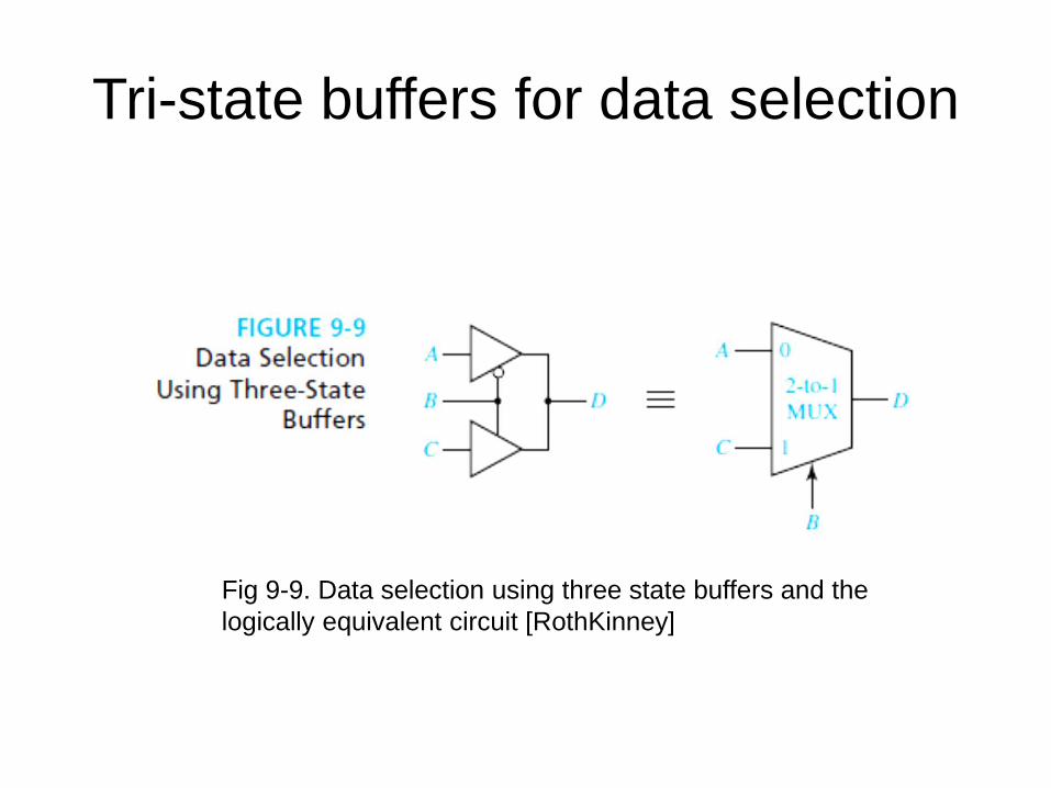
Tri-state buffers for data selection
Fig 9-9. Data selection using three state buffers and the
logically equivalent circuit [RothKinney]
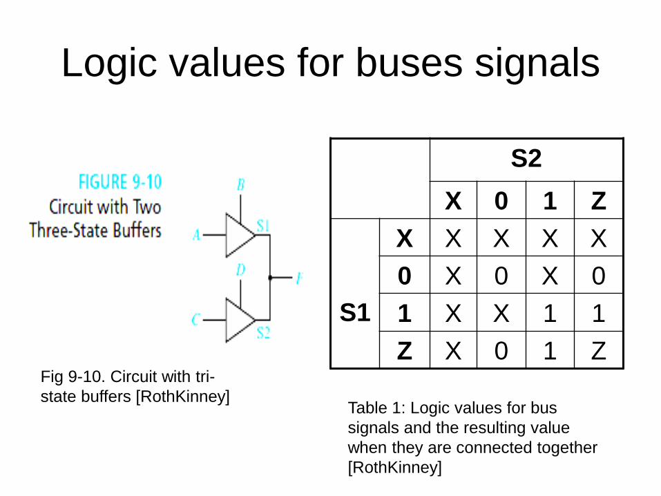
Logic values for buses signals
S2
X 0 1 Z
S1
X X X X X
0 X 0 X 0
1 X X 1 1
Z X 0 1 Z
Table 1: Logic values for bus
signals and the resulting value
when they are connected together
[RothKinney]
Fig 9-10. Circuit with tri-
state buffers [RothKinney]
Interpretation of table 1
• Normally we do not connect several circuit outputs together
• If there are situations when we have to, we use tri-state buffers and an arbitration mechanism that ensures that only one output has a logic value, and the other outputs are in Hi-Z
• If the arbitration mechanism fails, two active (i.e, not in Hi-Z) circuits outputs can be connected together
• If they have different logic values (0 and 1), the resulted value is unknown, denoted X – in the table 0 and 1 give X
• Such an unknown value propagates, in the sense that, if a third circuit output is also connected, the resulting value will remain X– In table 1, X and any value give X
• From the table it seems ok to connect together two circuit outputs that are both 0 or both 1
• In reality it is not ok, mainly due to transition periods (when circuits change value)
• When no output is active, the resulted value will be Hi-Z
Table 1 and VHDL
• In VHDL we cannot connect two circuit outputs together – a signal cannot have more than one source (driver)
• If we need a signal with more than one driver, it is declared in a special way and it has a resolution function, that determines the resulted value of the signal
• A resolution function works like described in table 1:– An X results from a 0 and a 1
– X is stronger than any other value
– 0 and 1 are stronger than Z
– The final result will be Z only if all values are Z
Bi-directional pins
• Circuit from figure 9.11 shows an example of using tri-state buffers as a means to select one of several (4 in this case) sources
• The circuit behaves like a 4:1 MUX
• Figure 9.12 shows another utilization of tri-state buffers, for circuits with bi-directional pins– A pin is used both for input and output, but not in the
same time
– Such situation appears e.g. for data buses at microprocessors
– Multiplexing reduces the number of pins, which reduces the cost of the circuit
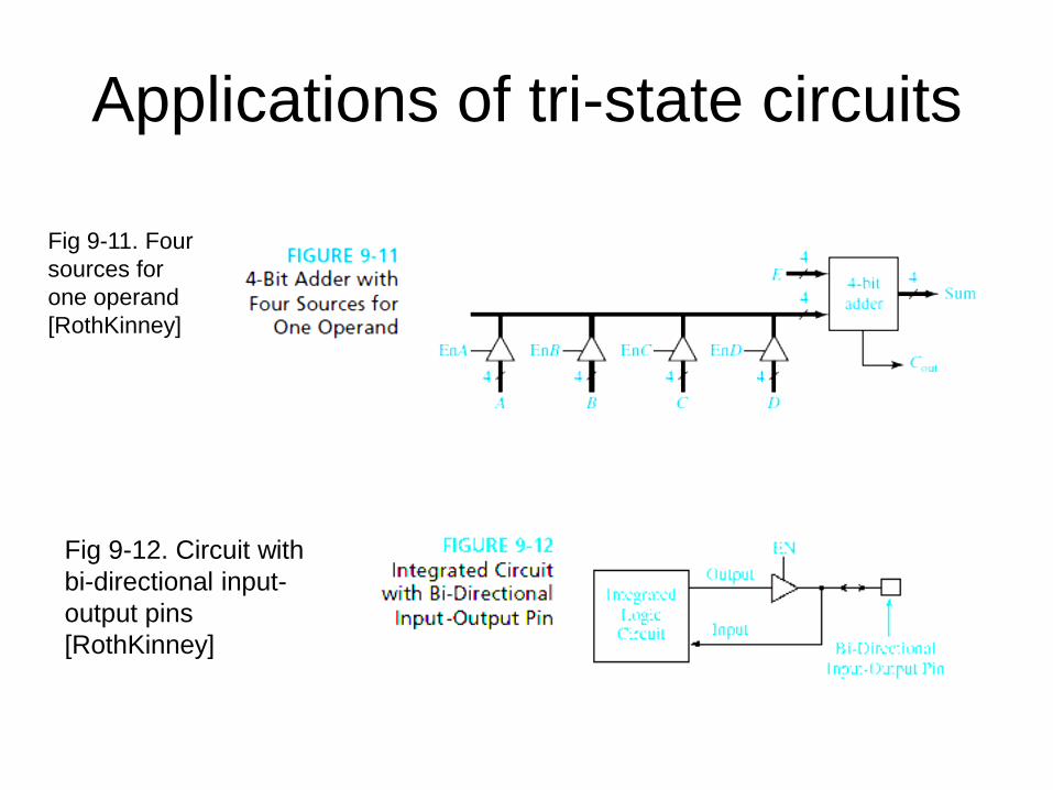
Applications of tri-state circuits
Fig 9-11. Four
sources for
one operand
[RothKinney]
Fig 9-12. Circuit with
bi-directional input-
output pins
[RothKinney]
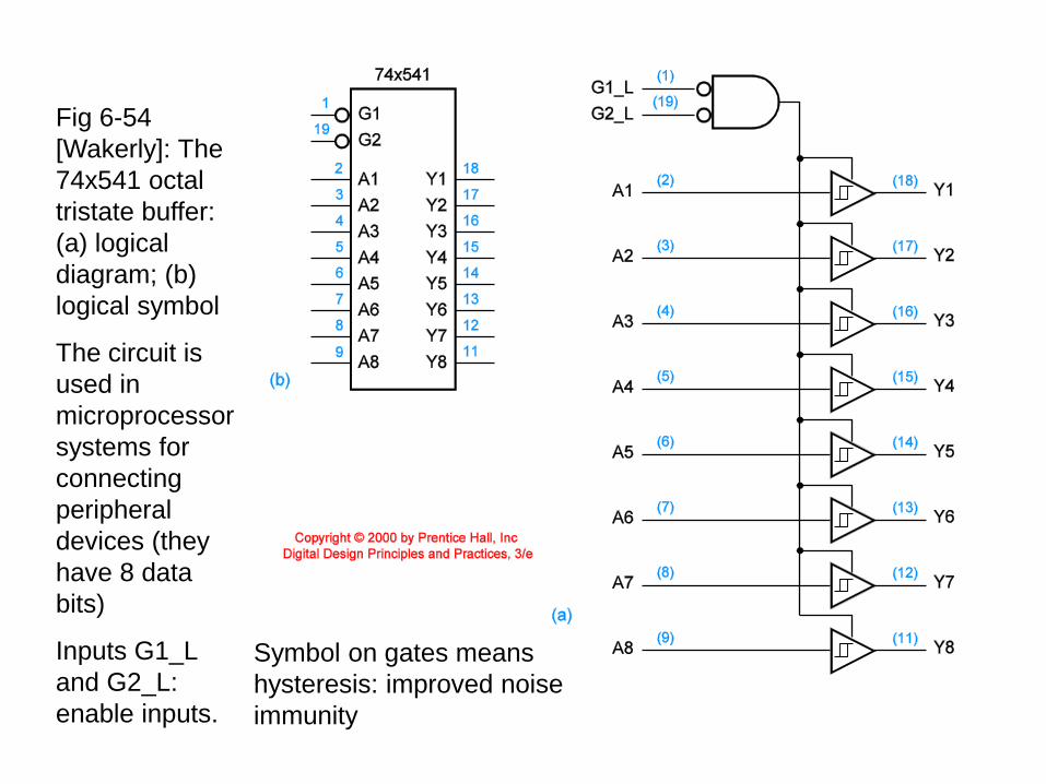
Fig 6-54
[Wakerly]: The
74x541 octal
tristate buffer:
(a) logical
diagram; (b)
logical symbol
The circuit is
used in
microprocessor
systems for
connecting
peripheral
devices (they
have 8 data
bits)
Inputs G1_L
and G2_L:
enable inputs.
Symbol on gates means
hysteresis: improved noise
immunity
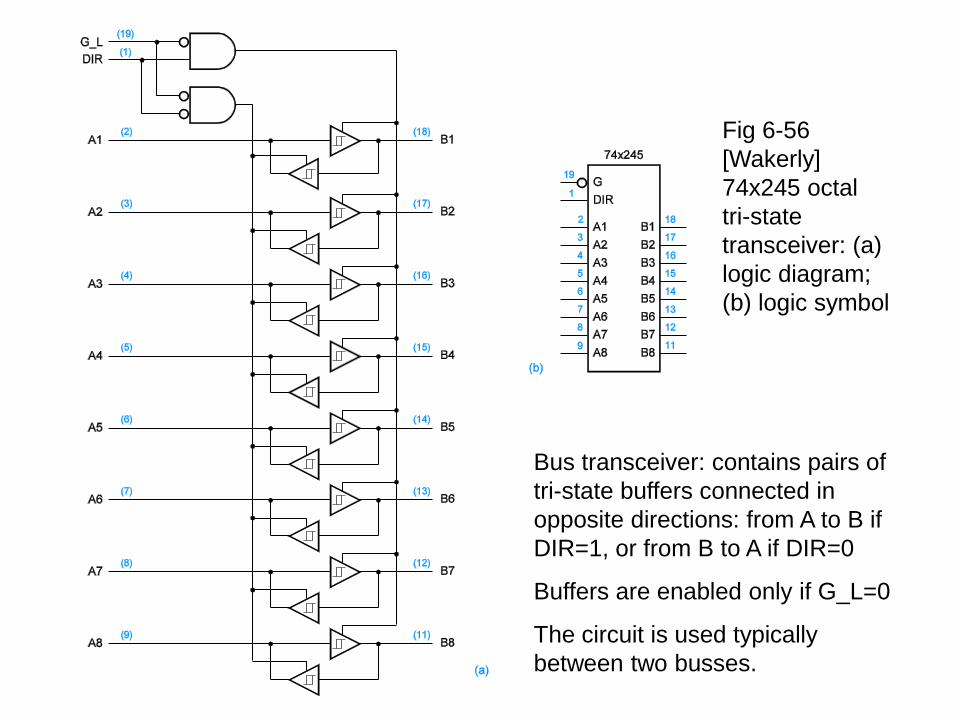
Fig 6-56
[Wakerly]
74x245 octal
tri-state
transceiver: (a)
logic diagram;
(b) logic symbol
Bus transceiver: contains pairs of
tri-state buffers connected in
opposite directions: from A to B if
DIR=1, or from B to A if DIR=0
Buffers are enabled only if G_L=0
The circuit is used typically
between two busses.
Decoders and Encoders
• Figure 9.13 shows a 3-to-8 decoder– The inputs represent a 3-bits binary number (between 0 and 7)
– The active output corresponds to the decimal representation of the input number (e.g, if input is 101, output 5 will be active)
• Exactly one output will be active for each input combination
• The decoder generates all the minterms for three input variables
• In general a n-to-2n decoder generates all minterms for nvariables
• The outputs are given by the equations yi=mi (for non-inverting outputs) and yi=mi’=Mi for inverting outputs
• Figure 9.14 shows a 4-to-10 decoder with inverted outputs: logic diagram, block diagram and truth table
• The 4-to-10 decoders do not generate all possible minterms
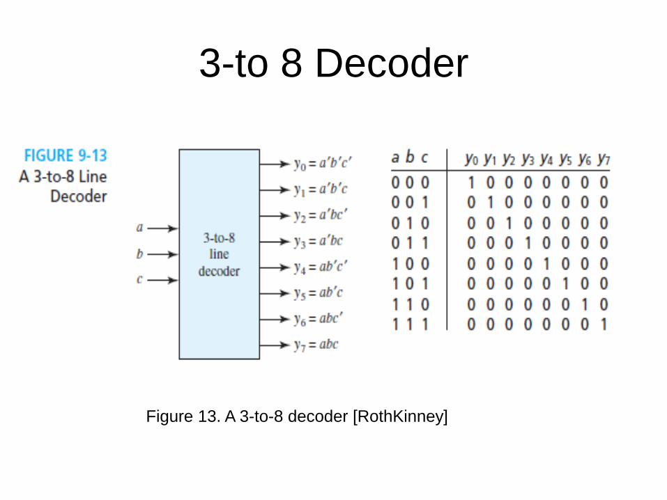
3-to 8 Decoder
Figure 13. A 3-to-8 decoder [RothKinney]
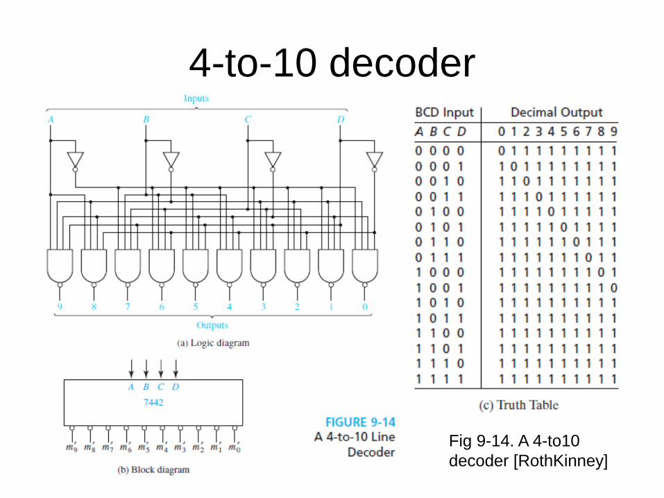
4-to-10 decoder
Fig 9-14. A 4-to10
decoder [RothKinney]
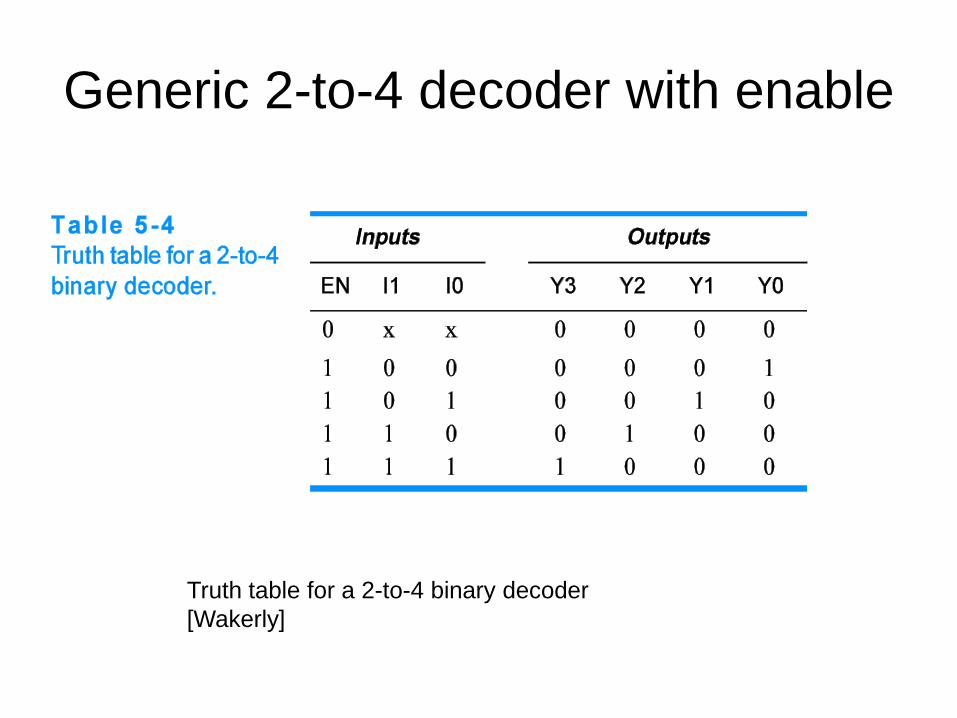
Generic 2-to-4 decoder with enable
Truth table for a 2-to-4 binary decoder
[Wakerly]
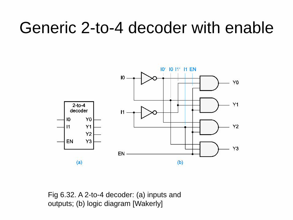
Generic 2-to-4 decoder with enable
Fig 6.32. A 2-to-4 decoder: (a) inputs and
outputs; (b) logic diagram [Wakerly]
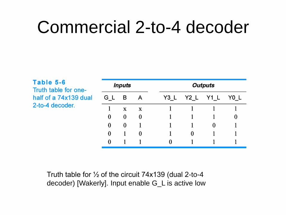
Commercial 2-to-4 decoder
Truth table for ½ of the circuit 74x139 (dual 2-to-4
decoder) [Wakerly]. Input enable G_L is active low
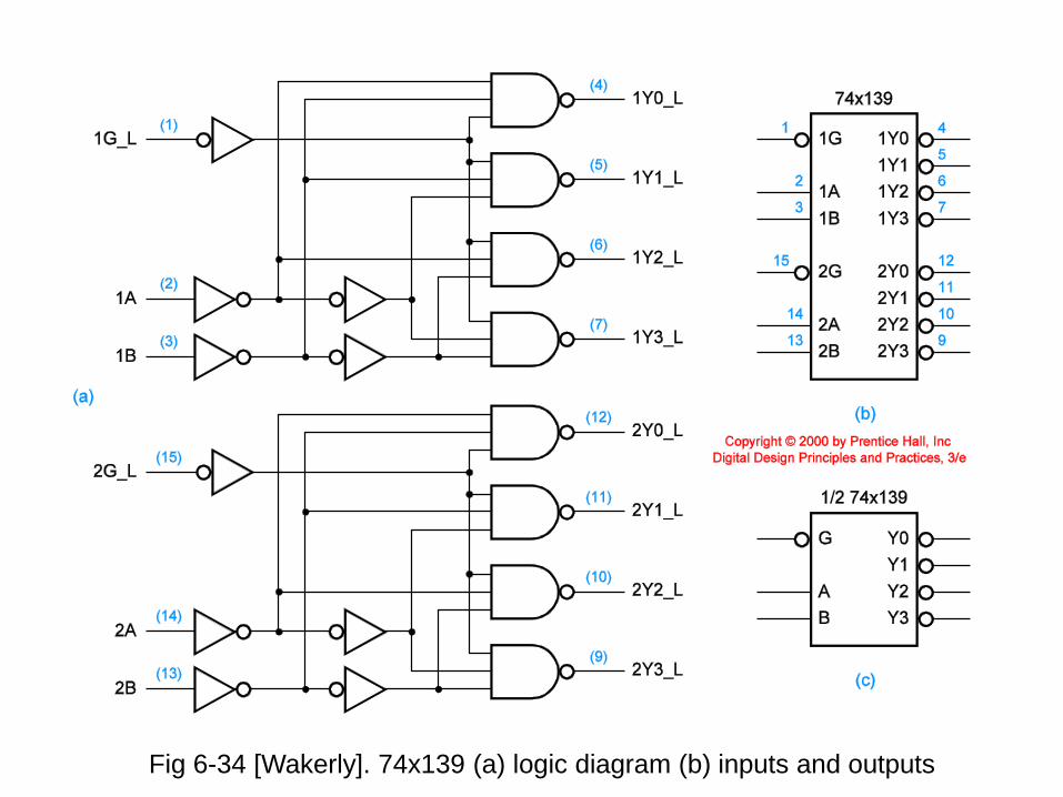
Fig 6-34 [Wakerly]. 74x139 (a) logic diagram (b) inputs and outputs
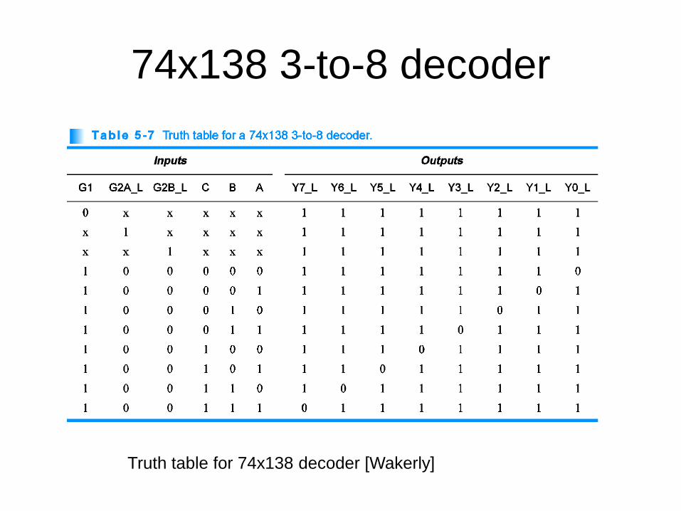
74x138 3-to-8 decoder
Truth table for 74x138 decoder [Wakerly]
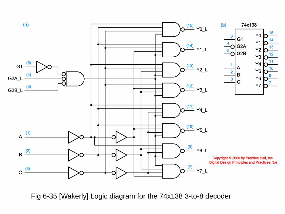
Fig 6-35 [Wakerly] Logic diagram for the 74x138 3-to-8 decoder
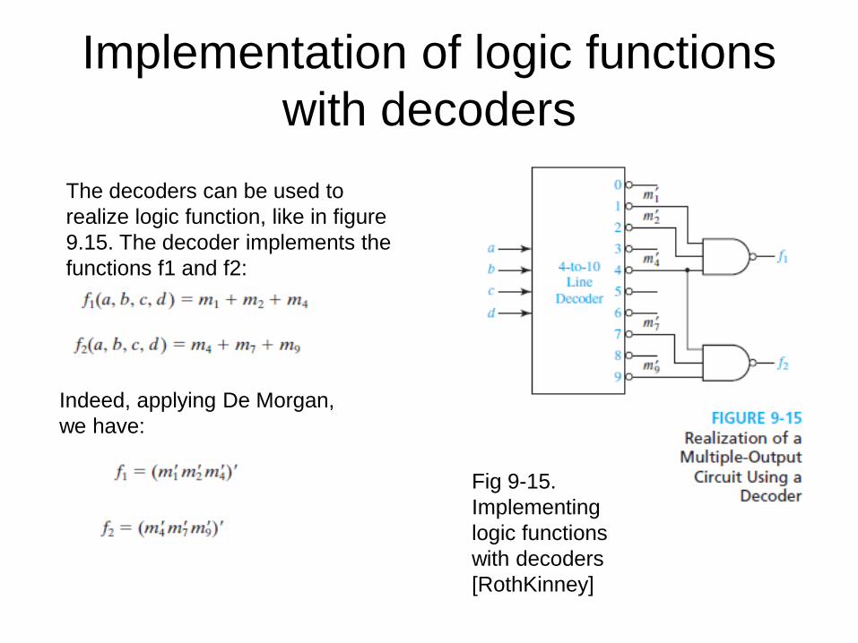
Implementation of logic functions
with decoders
The decoders can be used to
realize logic function, like in figure
9.15. The decoder implements the
functions f1 and f2:
Indeed, applying De Morgan,
we have:
Fig 9-15.
Implementing
logic functions
with decoders
[RothKinney]
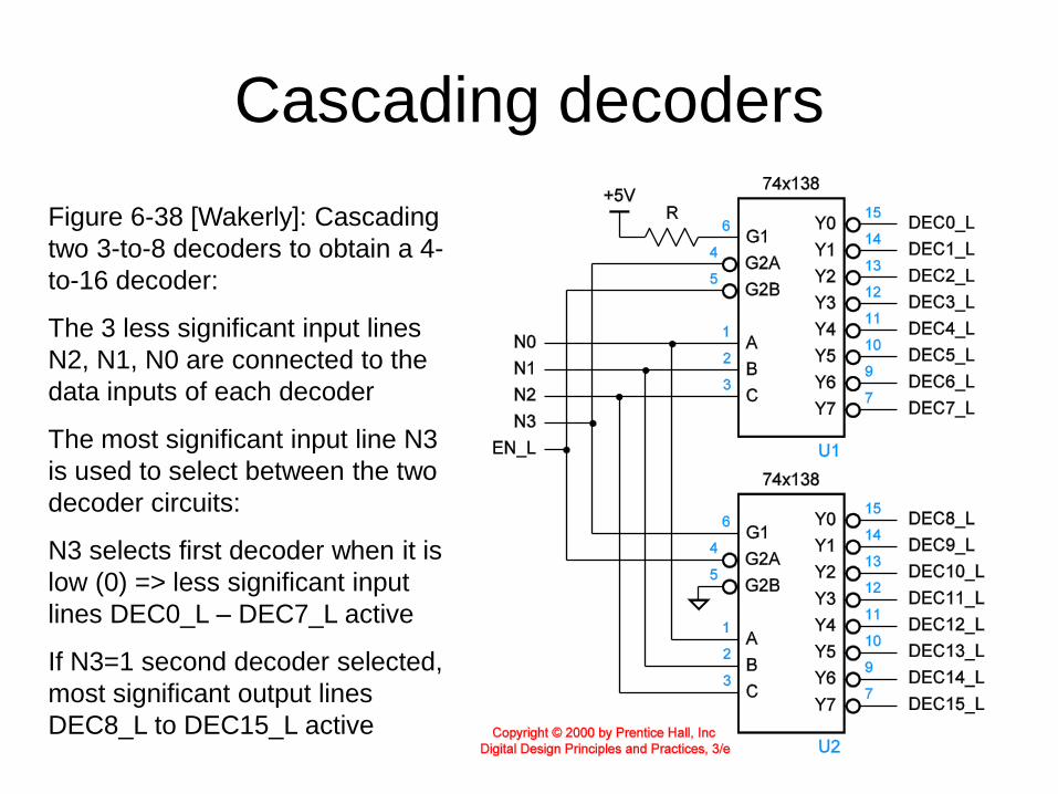
Cascading decoders
Figure 6-38 [Wakerly]: Cascading
two 3-to-8 decoders to obtain a 4-
to-16 decoder:
The 3 less significant input lines
N2, N1, N0 are connected to the
data inputs of each decoder
The most significant input line N3
is used to select between the two
decoder circuits:
N3 selects first decoder when it is
low (0) => less significant input
lines DEC0_L – DEC7_L active
If N3=1 second decoder selected,
most significant output lines
DEC8_L to DEC15_L active
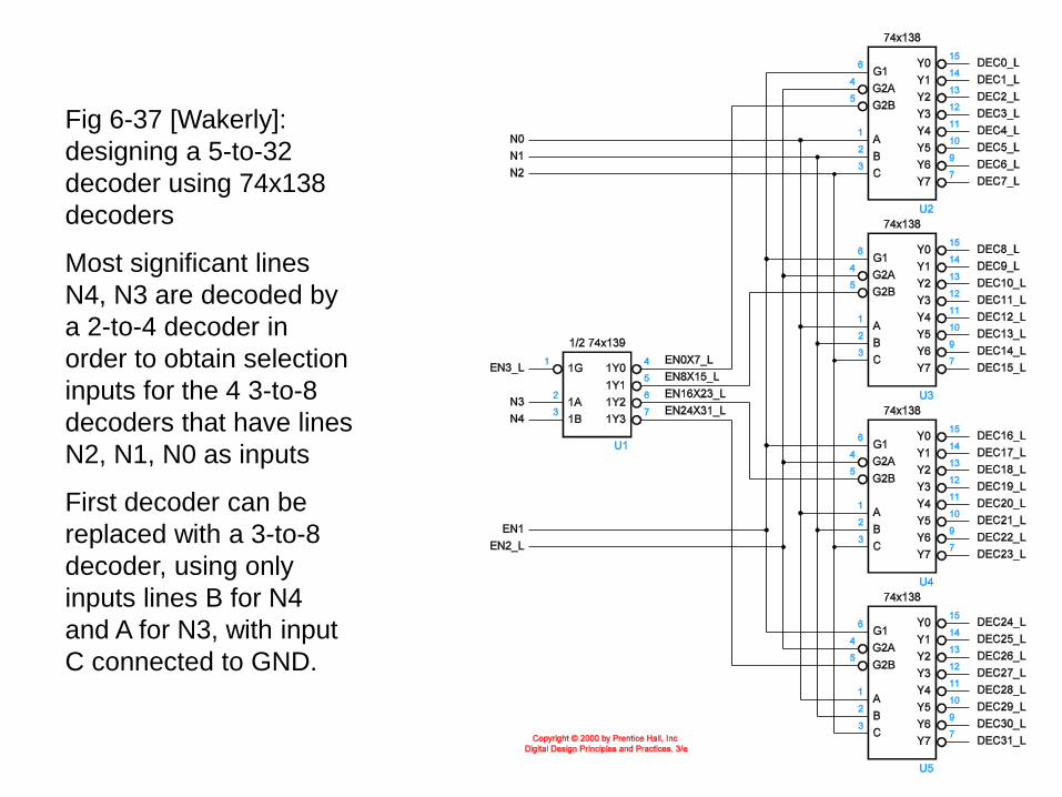
Fig 6-37 [Wakerly]:
designing a 5-to-32
decoder using 74x138
decoders
Most significant lines
N4, N3 are decoded by
a 2-to-4 decoder in
order to obtain selection
inputs for the 4 3-to-8
decoders that have lines
N2, N1, N0 as inputs
First decoder can be
replaced with a 3-to-8
decoder, using only
inputs lines B for N4
and A for N3, with input
C connected to GND.
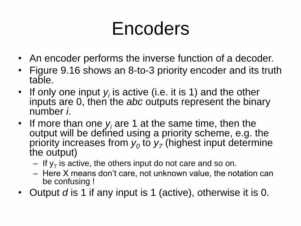
Encoders
• An encoder performs the inverse function of a decoder.
• Figure 9.16 shows an 8-to-3 priority encoder and its truth table.
• If only one input yi is active (i.e. it is 1) and the other inputs are 0, then the abc outputs represent the binary number i.
• If more than one yi are 1 at the same time, then the output will be defined using a priority scheme, e.g. the priority increases from y0 to y7 (highest input determine the output)– If y7 is active, the others input do not care and so on.
– Here X means don’t care, not unknown value, the notation can be confusing !
• Output d is 1 if any input is 1 (active), otherwise it is 0.
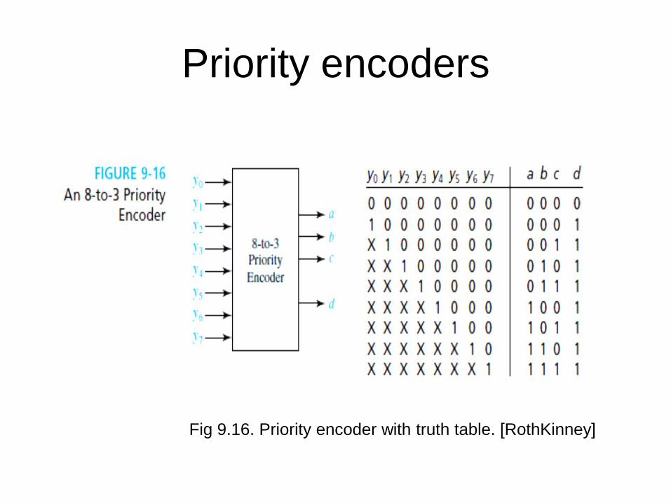
Priority encoders
Fig 9.16. Priority encoder with truth table. [RothKinney]
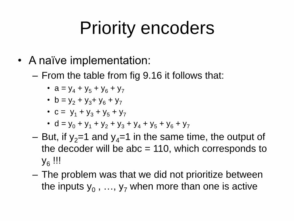
Priority encoders
• A naïve implementation:
– From the table from fig 9.16 it follows that:
• a = y4 + y5 + y6 + y7
• b = y2 + y3+ y6 + y7
• c = y1 + y3 + y5 + y7
• d = y0 + y1 + y2 + y3 + y4 + y5 + y6 + y7
– But, if y2=1 and y4=1 in the same time, the output of
the decoder will be abc = 110, which corresponds to
y6 !!!
– The problem was that we did not prioritize between
the inputs y0 , …, y7 when more than one is active
Priority encoders
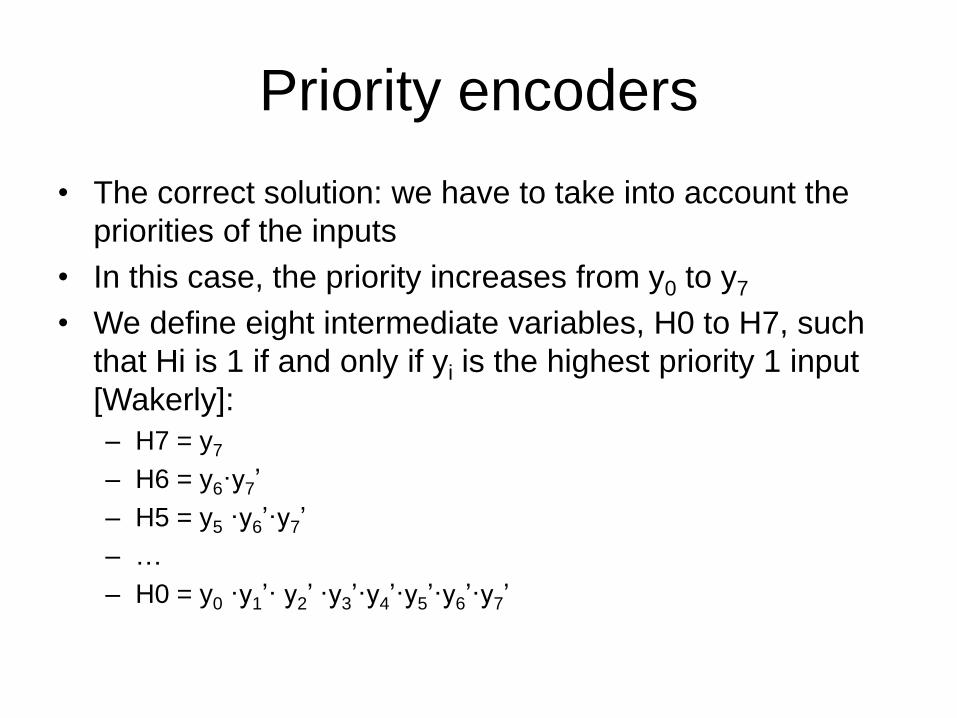
• The correct solution: we have to take into account the
priorities of the inputs
• In this case, the priority increases from y0 to y7
• We define eight intermediate variables, H0 to H7, such
that Hi is 1 if and only if yi is the highest priority 1 input
[Wakerly]:
– H7 = y7
– H6 = y6·y7’
– H5 = y5 ·y6’·y7’
– …
– H0 = y0 ·y1’· y2’ ·y3’·y4’·y5’·y6’·y7’
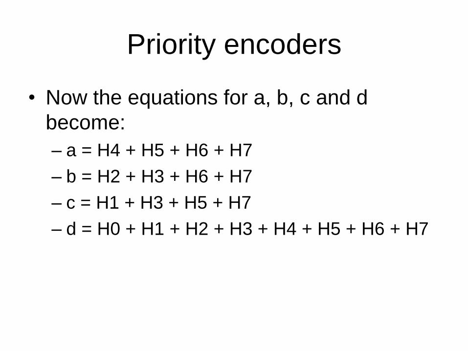
Priority encoders
• Now the equations for a, b, c and d
become:
– a = H4 + H5 + H6 + H7
– b = H2 + H3 + H6 + H7
– c = H1 + H3 + H5 + H7
– d = H0 + H1 + H2 + H3 + H4 + H5 + H6 + H7
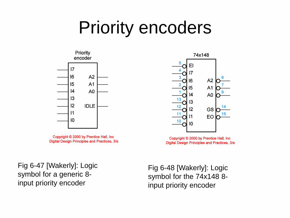
Priority encoders
Fig 6-47 [Wakerly]: Logic
symbol for a generic 8-
input priority encoder
Fig 6-48 [Wakerly]: Logic
symbol for the 74x148 8-
input priority encoder
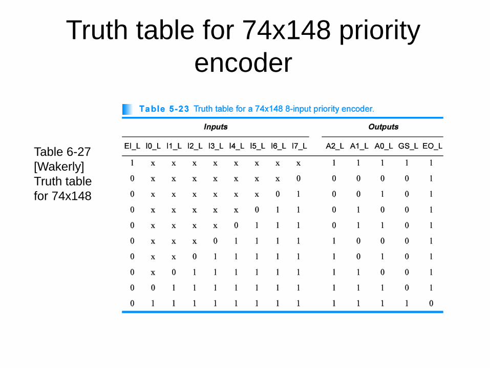
Truth table for 74x148 priority
encoder
Table 6-27
[Wakerly]
Truth table
for 74x148
74x148 priority encoder
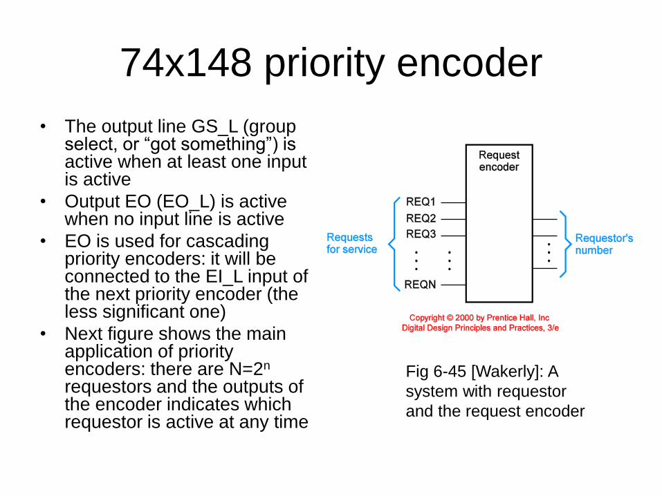
• The output line GS_L (group select, or “got something”) is active when at least one input is active
• Output EO (EO_L) is active when no input line is active
• EO is used for cascading priority encoders: it will be connected to the EI_L input of the next priority encoder (the less significant one)
• Next figure shows the main application of priority encoders: there are N=2n
requestors and the outputs of the encoder indicates which requestor is active at any time
Fig 6-45 [Wakerly]: A
system with requestor
and the request encoder
Commercial multiplexers.
Applications of multiplexers and
demultiplexers
• Commercial multiplexers
• Expanding multiplexers
• Multiplexers, demultiplexers and busses
• Using Shannon expansion theorem for
designing with multiplexers
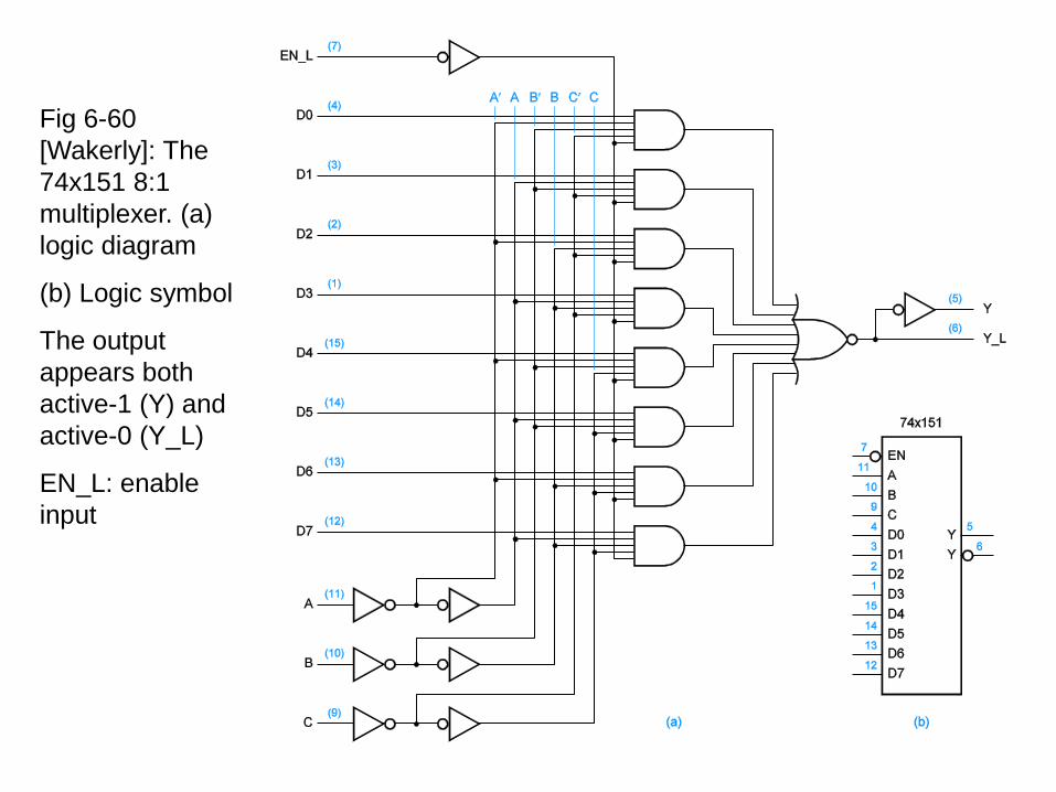
Fig 6-60
[Wakerly]: The
74x151 8:1
multiplexer. (a)
logic diagram
(b) Logic symbol
The output
appears both
active-1 (Y) and
active-0 (Y_L)
EN_L: enable
input
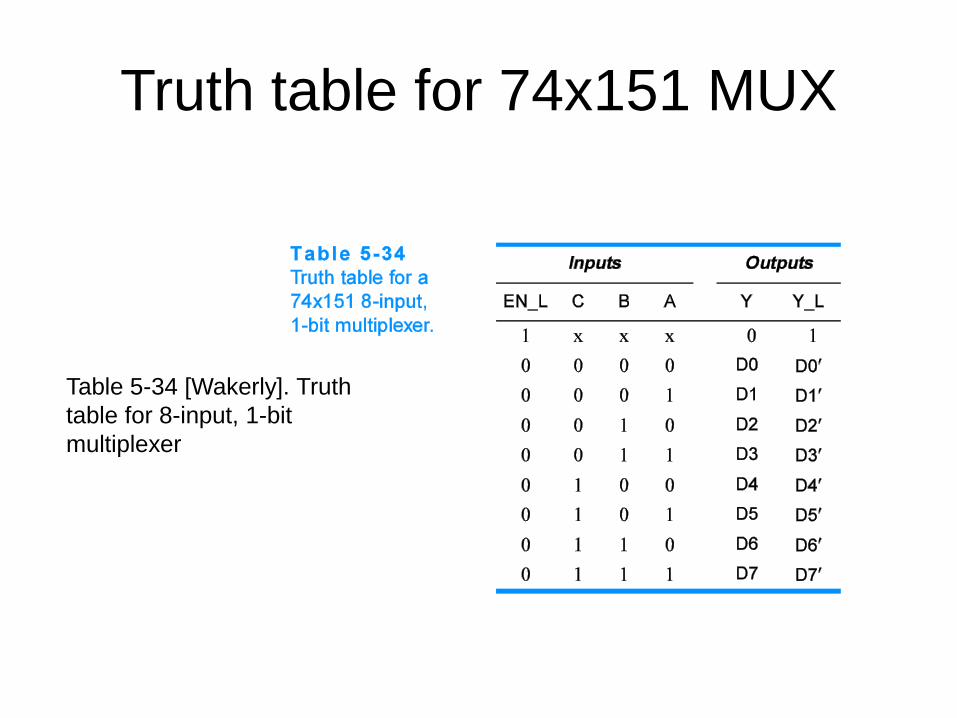
Truth table for 74x151 MUX
Table 5-34 [Wakerly]. Truth
table for 8-input, 1-bit
multiplexer
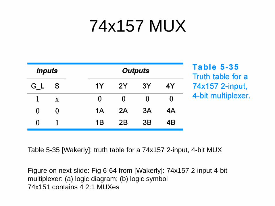
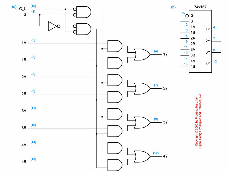
74x157 MUX
Table 5-35 [Wakerly]: truth table for a 74x157 2-input, 4-bit MUX
Figure on next slide: Fig 6-64 from [Wakerly]: 74x157 2-input 4-bit
multiplexer: (a) logic diagram; (b) logic symbol
74x151 contains 4 2:1 MUXes
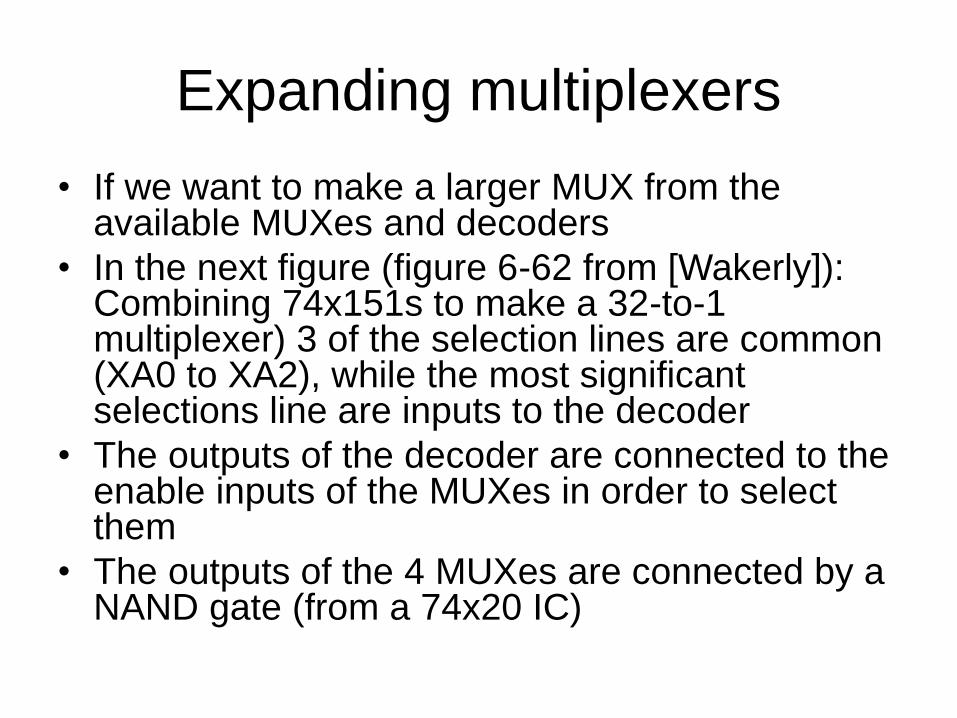
Expanding multiplexers
• If we want to make a larger MUX from the available MUXes and decoders
• In the next figure (figure 6-62 from [Wakerly]): Combining 74x151s to make a 32-to-1 multiplexer) 3 of the selection lines are common (XA0 to XA2), while the most significant selections line are inputs to the decoder
• The outputs of the decoder are connected to the enable inputs of the MUXes in order to select them
• The outputs of the 4 MUXes are connected by a NAND gate (from a 74x20 IC)
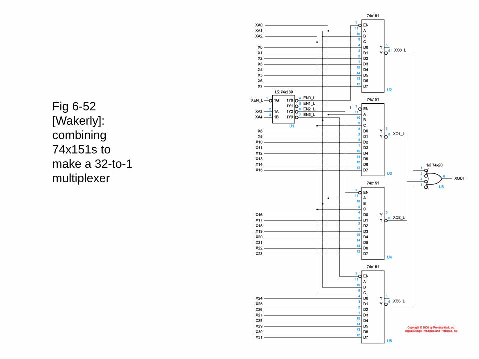
Fig 6-52
[Wakerly]:
combining
74x151s to
make a 32-to-1
multiplexer
Multiplexers, demultiplexers and
buses • A demultiplexer (DEMUX) performs the opposite function
of a multiplexer: – Has one data input
– Has n selection inputs
– And 2n outputs
– The input will be connected to the output who’s number is given by the binary number that represents the selection inputs
• A MUX can be used to select 1-out-of-n sources of data and transmit it on a bus
• At the other end of the bus a DEMUX can be used to route the bus data to one of the destinations
• A demultiplexer can be implemented with a decoder (e.g. with a 74x139 2-to-4 decoder, or with a 74x138 3-to-8 decoder)
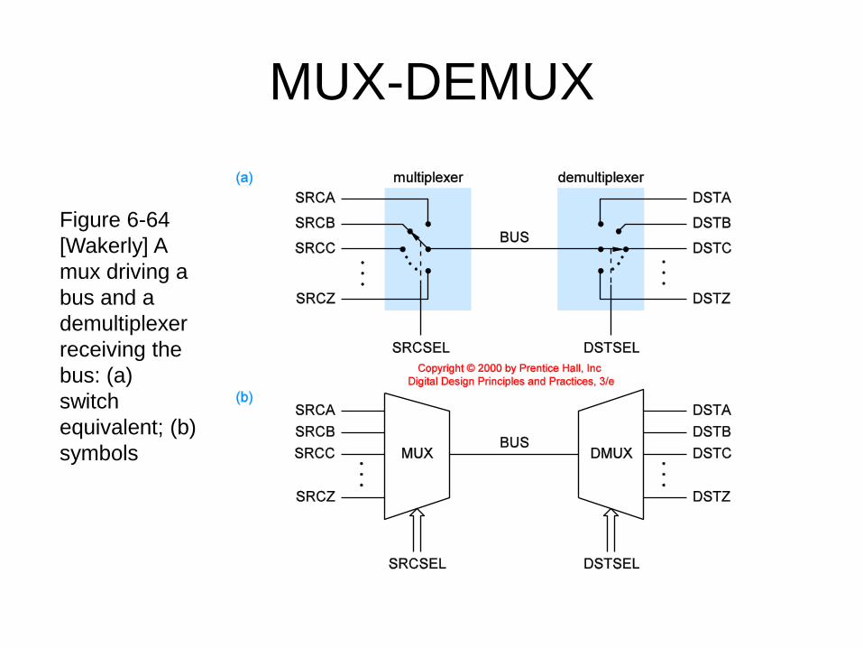
MUX-DEMUX
Figure 6-64
[Wakerly] A
mux driving a
bus and a
demultiplexer
receiving the
bus: (a)
switch
equivalent; (b)
symbols
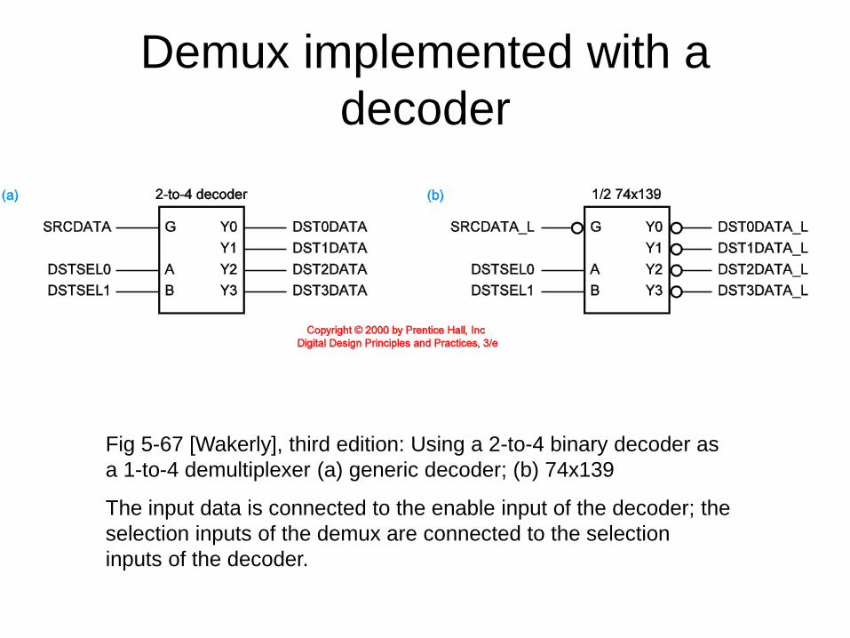
Demux implemented with a
decoder
Fig 5-67 [Wakerly], third edition: Using a 2-to-4 binary decoder as
a 1-to-4 demultiplexer (a) generic decoder; (b) 74x139
The input data is connected to the enable input of the decoder; the
selection inputs of the demux are connected to the selection
inputs of the decoder.
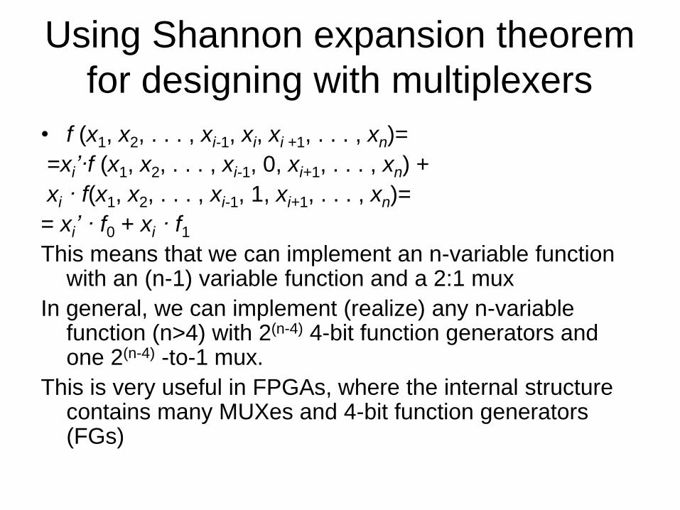
Using Shannon expansion theorem
for designing with multiplexers
• f (x1, x2, . . . , xi-1, xi, xi +1, . . . , xn)=
=xi’·f (x1, x2, . . . , xi-1, 0, xi+1, . . . , xn) +
xi · f(x1, x2, . . . , xi-1, 1, xi+1, . . . , xn)=
= xi’ · f0 + xi · f1This means that we can implement an n-variable function
with an (n-1) variable function and a 2:1 mux
In general, we can implement (realize) any n-variable function (n>4) with 2(n-4) 4-bit function generators and one 2(n-4) -to-1 mux.
This is very useful in FPGAs, where the internal structure contains many MUXes and 4-bit function generators (FGs)
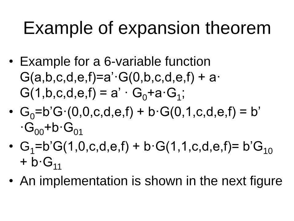
Example of expansion theorem
• Example for a 6-variable function
G(a,b,c,d,e,f)=a’·G(0,b,c,d,e,f) + a·
G(1,b,c,d,e,f) = a’ · G0+a·G1;
• G0=b’G·(0,0,c,d,e,f) + b·G(0,1,c,d,e,f) = b’
·G00+b·G01
• G1=b’G(1,0,c,d,e,f) + b·G(1,1,c,d,e,f)= b’G10
+ b·G11
• An implementation is shown in the next figure
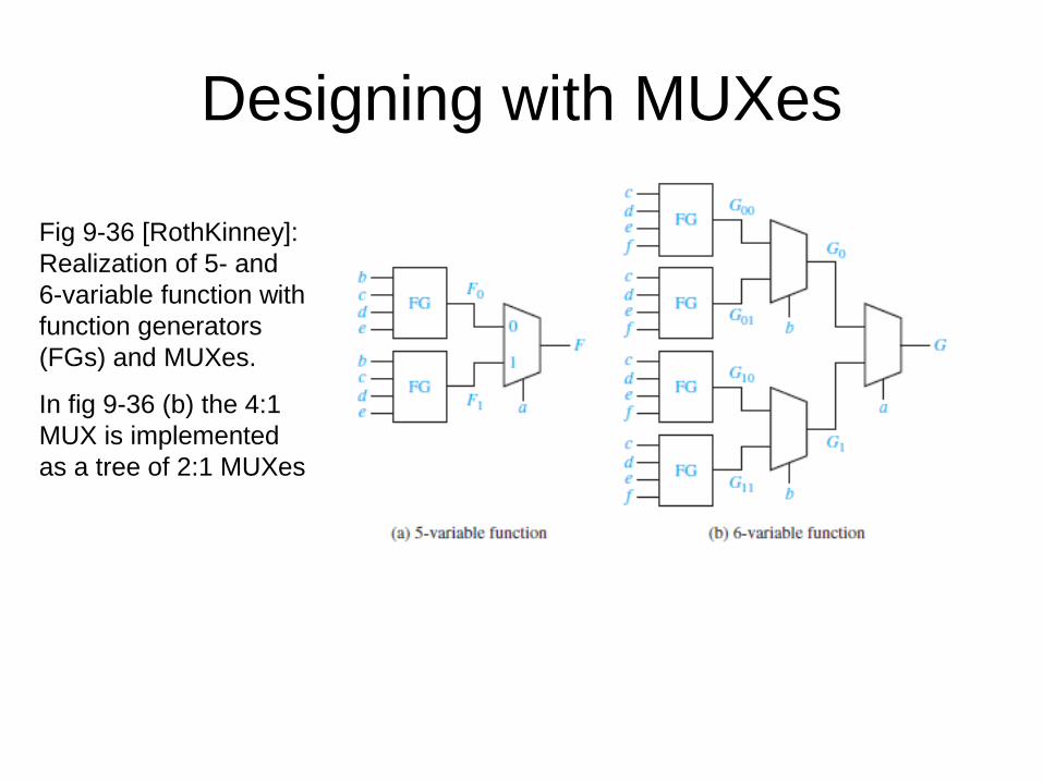
Designing with MUXes
Fig 9-36 [RothKinney]:
Realization of 5- and
6-variable function with
function generators
(FGs) and MUXes.
In fig 9-36 (b) the 4:1
MUX is implemented
as a tree of 2:1 MUXes
Read-Only Memories
• A read-only memory (ROM) is an array of semiconductor devices that are interconnected to store an array of binary data
• Once stored in the ROM, the binary data can be read, but cannot be modified (under normal operating conditions)
• A ROM implements (i.e. stores) the truth table of a function (or of several functions)
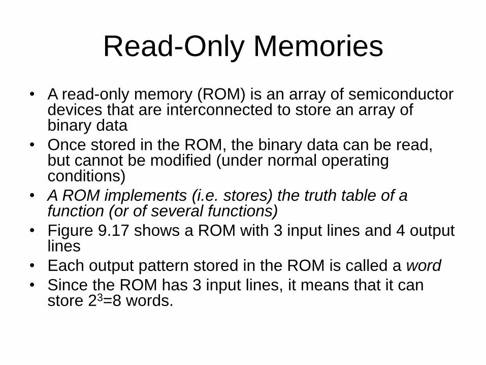
• Figure 9.17 shows a ROM with 3 input lines and 4 output lines
• Each output pattern stored in the ROM is called a word
• Since the ROM has 3 input lines, it means that it can store 23=8 words.
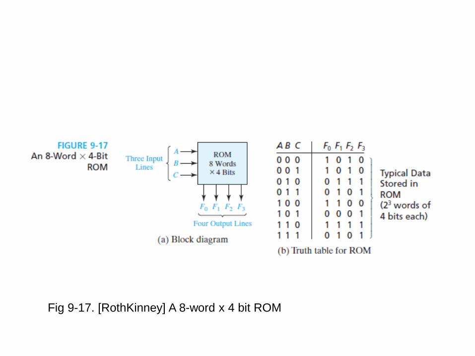
Fig 9-17. [RothKinney] A 8-word x 4 bit ROM
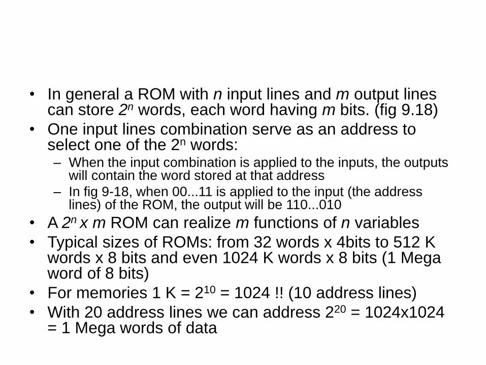
• In general a ROM with n input lines and m output lines can store 2n words, each word having m bits. (fig 9.18)
• One input lines combination serve as an address to select one of the 2n words:– When the input combination is applied to the inputs, the outputs
will contain the word stored at that address
– In fig 9-18, when 00...11 is applied to the input (the address lines) of the ROM, the output will be 110...010
• A 2n x m ROM can realize m functions of n variables
• Typical sizes of ROMs: from 32 words x 4bits to 512 K words x 8 bits and even 1024 K words x 8 bits (1 Mega word of 8 bits)
• For memories 1 K = 210 = 1024 !! (10 address lines)
• With 20 address lines we can address 220 = 1024x1024 = 1 Mega words of data
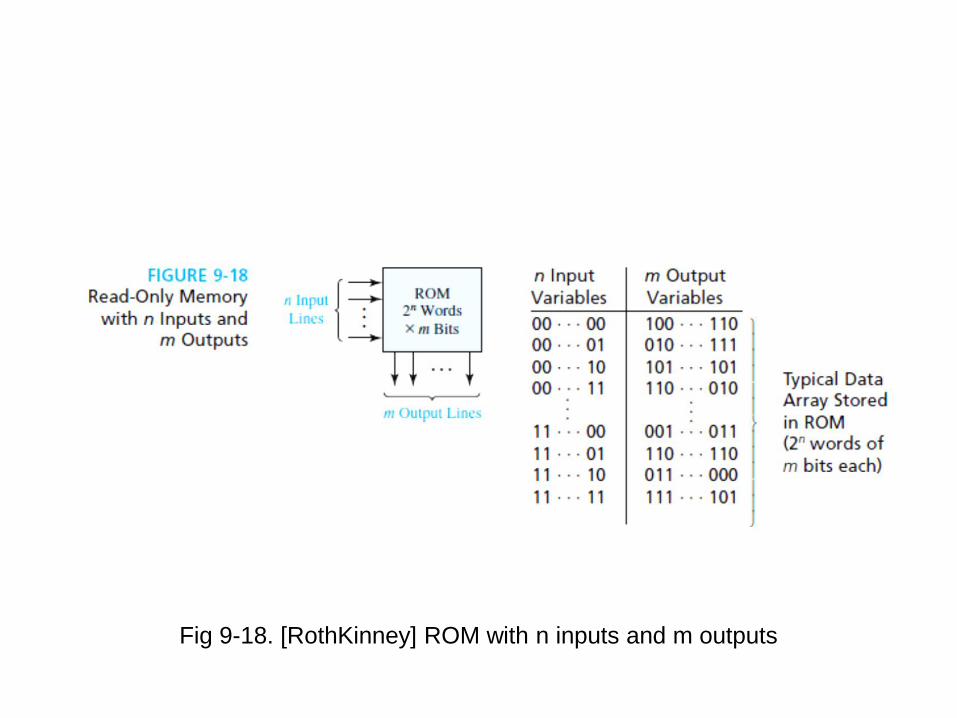
Fig 9-18. [RothKinney] ROM with n inputs and m outputs
Basic ROM structure
Fig 9-19 [RothKinney]
Basic ROM structure
A ROM consists of a
decoder and a memory
array (see fig 9-19)
When a pattern of 0s
and 1s is applied to the
decoder inputs, exactly
one of the decoder’s
outputs will be active.
The active output line of
the decoder will select a
word from the memory
array.
The selected word will
appear at the outputs of
the ROM.
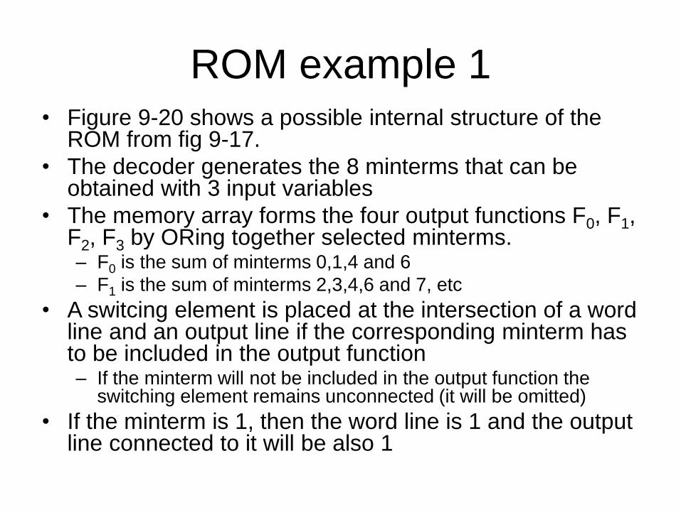
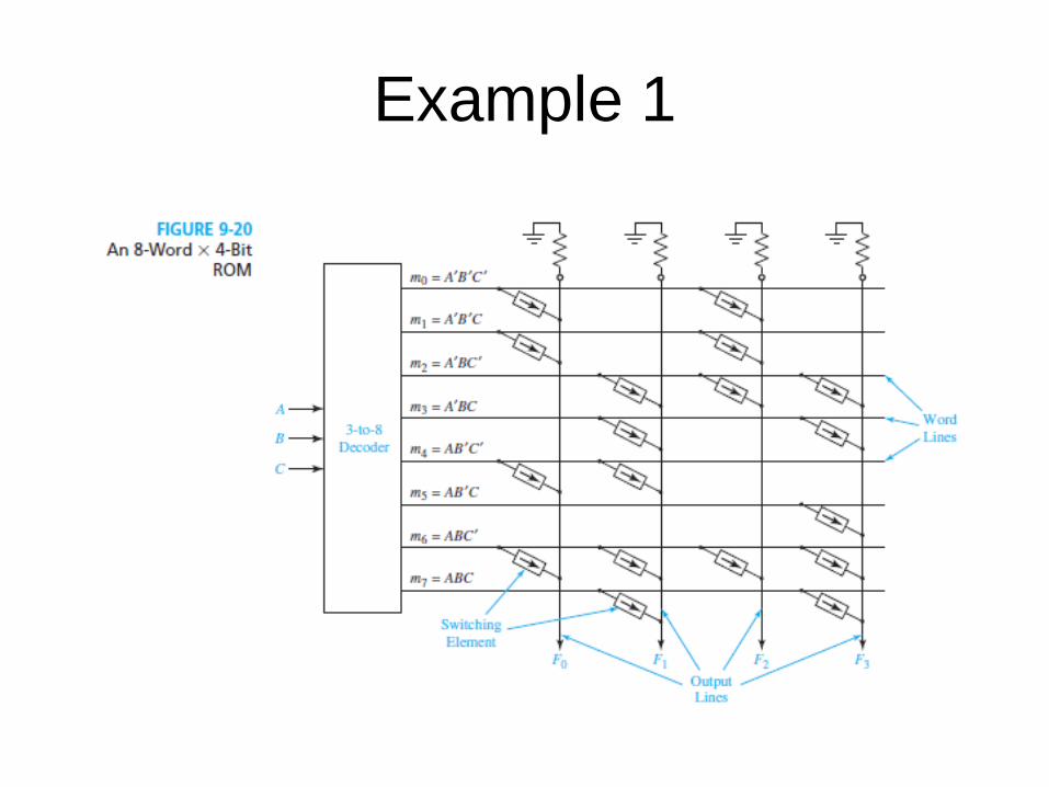
ROM example 1• Figure 9-20 shows a possible internal structure of the
ROM from fig 9-17.
• The decoder generates the 8 minterms that can be obtained with 3 input variables
• The memory array forms the four output functions F0, F1, F2, F3 by ORing together selected minterms.– F0 is the sum of minterms 0,1,4 and 6
– F1 is the sum of minterms 2,3,4,6 and 7, etc
• A switcing element is placed at the intersection of a word line and an output line if the corresponding minterm has to be included in the output function– If the minterm will not be included in the output function the
switching element remains unconnected (it will be omitted)
• If the minterm is 1, then the word line is 1 and the output line connected to it will be also 1
Example 1
• If none of the word lines connected to an output line is 1, then the pull-down resistors will cause the output to be 0
• In this way the switching elements form an OR array: an OR gate for each of the output lines
• The minterms that form a function are connected to the output line that corresponds to that function.
Example 1
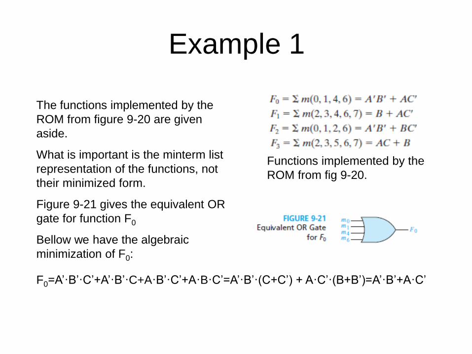
Example 1
F0=A’·B’·C’+A’·B’·C+A·B’·C’+A·B·C’=A’·B’·(C+C’) + A·C’·(B+B’)=A’·B’+A·C’
Functions implemented by the
ROM from fig 9-20.
The functions implemented by the
ROM from figure 9-20 are given
aside.
What is important is the minterm list
representation of the functions, not
their minimized form.
Figure 9-21 gives the equivalent OR
gate for function F0
Bellow we have the algebraic
minimization of F0:
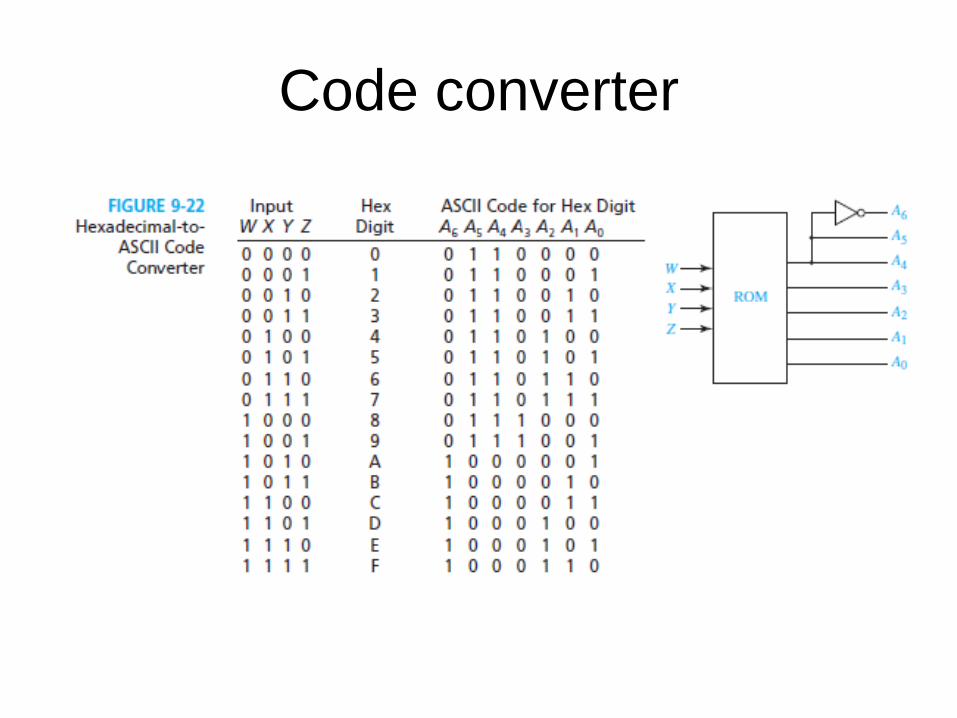
Another example: code converter
• Figure 9-22 shows the truth table and the logic circuit for a code converter that converts a 4-bit binary number to the ASCII representation of its hexadecimal digit
• ASCII: American Standard Code for Information Interchange: a 7-bits code for representing digits, letters and other characters.– The character A is represented by the combination 4116, or 100
0001 in binary, etc
• From the table we can see that A5=A4 and A6=A4’ => the ROM will have 4 input lines and 5 output lines (16 words by 5 bits)
• The switching elements at the intersections of rows and columns are marked by X’s: – An X indicates that the switching element is presented and
connected
– No X means that the corresponding element is absent or not connected
Code converter
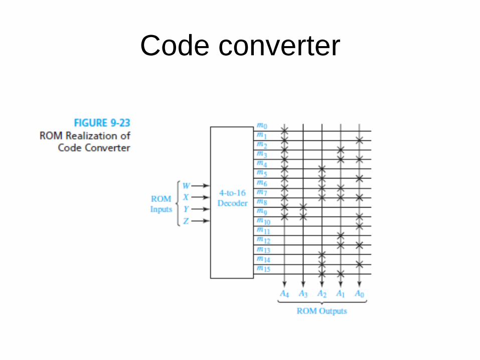
Code converter
Types of ROMs
• The most common types of ROMs are:– Mask-programmable ROMs
– Programmable ROMs (PROMs)
– Electrically erasable ROMs
• Mask programmable ROMs:– They are programmed at the time of manufacture
– Data is permanently stored and cannot be changed
– The presence or omission of the switching elements is realized with a mask
– The realization of a mask is expensive =>
– This type of ROM is economically feasible only for a large quantity
• PROMs: can be programmed by the user, but only once
EEPROMs
• Can be erased and re-programmed
• They use a special charge-storage mechanism to enable or disable the switching elements in the memory array
• They are programmed with a PROM programmer
• Data stored is permanent, until erase
• The erasing and reprogramming cycles are limited (100-1000 times)
• Programming voltages are higher than in normal operation
• Also, programming times are much higher than their normal delays)
• Flash memories are similar to EEPROMs, but they use a different charge-storage mechanism– Also, have built-in programming and erase capabilities => don’t
need a special programmer
Programmable Logic Devices
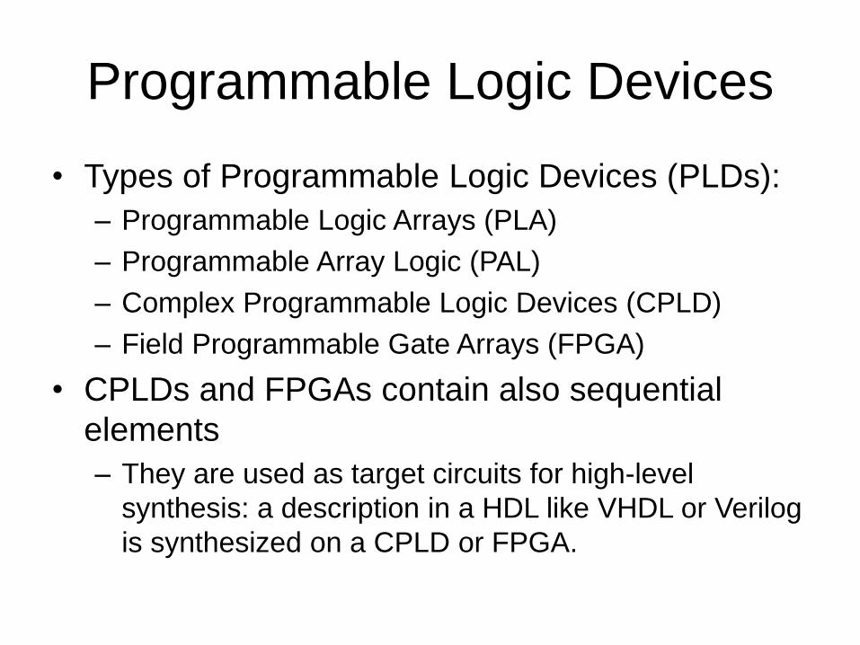
• Types of Programmable Logic Devices (PLDs):
– Programmable Logic Arrays (PLA)
– Programmable Array Logic (PAL)
– Complex Programmable Logic Devices (CPLD)
– Field Programmable Gate Arrays (FPGA)
• CPLDs and FPGAs contain also sequential
elements
– They are used as target circuits for high-level
synthesis: a description in a HDL like VHDL or Verilog
is synthesized on a CPLD or FPGA.
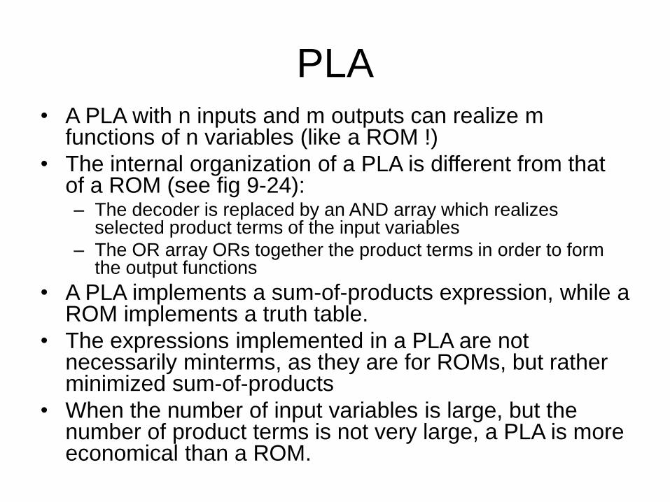
PLA• A PLA with n inputs and m outputs can realize m
functions of n variables (like a ROM !)
• The internal organization of a PLA is different from that of a ROM (see fig 9-24):– The decoder is replaced by an AND array which realizes
selected product terms of the input variables
– The OR array ORs together the product terms in order to form the output functions
• A PLA implements a sum-of-products expression, while a ROM implements a truth table.
• The expressions implemented in a PLA are not necessarily minterms, as they are for ROMs, but rather minimized sum-of-products
• When the number of input variables is large, but the number of product terms is not very large, a PLA is more economical than a ROM.
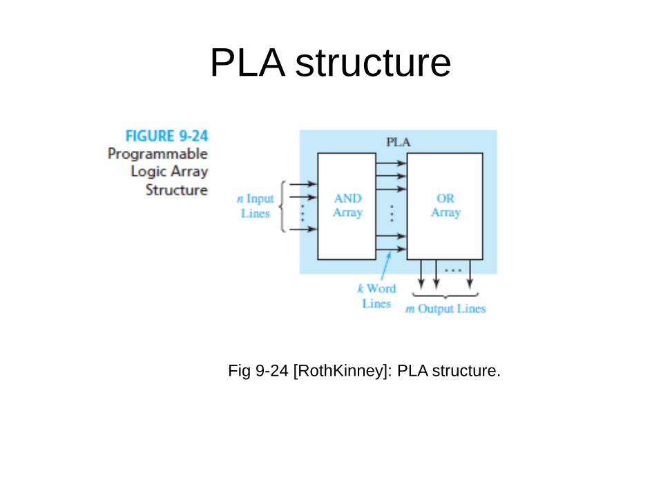
PLA structure
Fig 9-24 [RothKinney]: PLA structure.
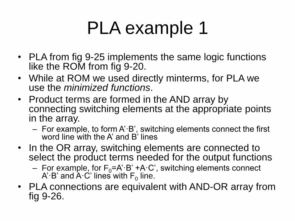
PLA example 1
• PLA from fig 9-25 implements the same logic functions like the ROM from fig 9-20.
• While at ROM we used directly minterms, for PLA we use the minimized functions.
• Product terms are formed in the AND array by connecting switching elements at the appropriate points in the array.– For example, to form A’·B’, switching elements connect the first
word line with the A’ and B’ lines
• In the OR array, switching elements are connected to select the product terms needed for the output functions– For example, for F0=A’·B’ +A·C’, switching elements connect
A’·B’ and A·C’ lines with F0 line.
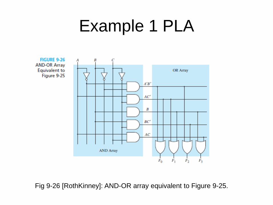
• PLA connections are equivalent with AND-OR array from fig 9-26.
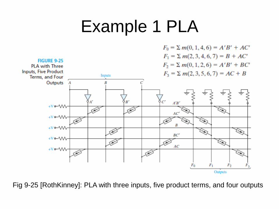
Example 1 PLA
Fig 9-25 [RothKinney]: PLA with three inputs, five product terms, and four outputs
Example 1 PLA
Fig 9-26 [RothKinney]: AND-OR array equivalent to Figure 9-25.
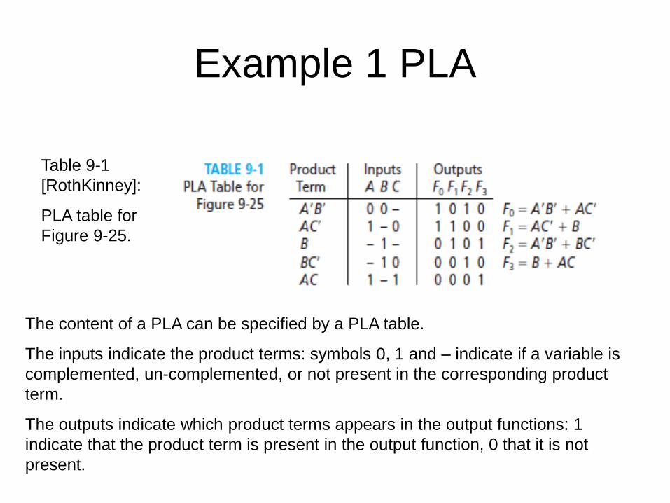
Example 1 PLA
Table 9-1
[RothKinney]:
PLA table for
Figure 9-25.
The content of a PLA can be specified by a PLA table.
The inputs indicate the product terms: symbols 0, 1 and – indicate if a variable is
complemented, un-complemented, or not present in the corresponding product
term.
The outputs indicate which product terms appears in the output functions: 1
indicate that the product term is present in the output function, 0 that it is not
present.
Example 2
• In example 2 we implement
equations (7-23b) from
[RothKinney], shown
below:
• f1=a’·b·d+a·b·d+a·b’·c’+b’·c
• f2=c+a’·b·d
• f3=b·c+a·b’·c’+a·b·d
• The PLA table is in fig 9-27
(a).
• The PLA structure is
given in Fig 9-27 (b).
• A dot at the intersection
of a word line and an
input or output line
indicates the presence of
a switching element in the
array
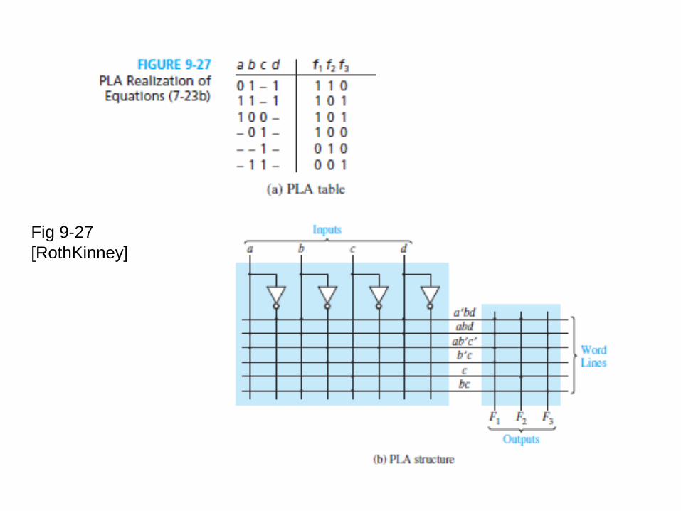
Fig 9-27
[RothKinney]
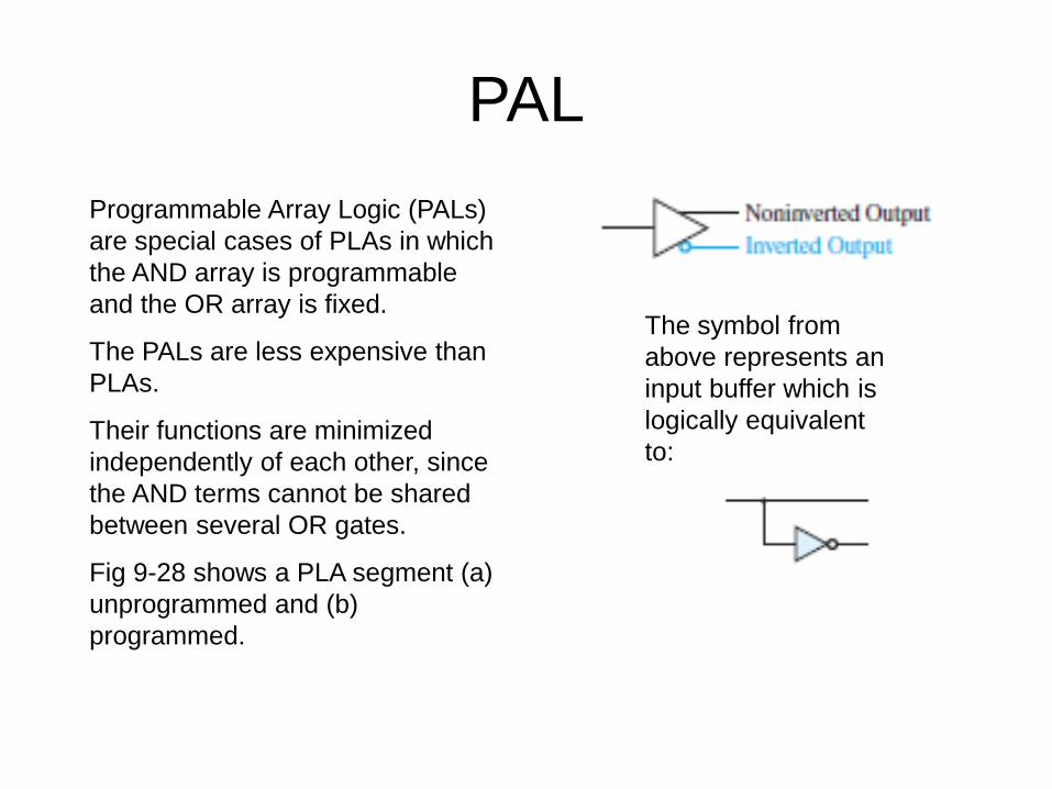
PAL
Programmable Array Logic (PALs)
are special cases of PLAs in which
the AND array is programmable
and the OR array is fixed.
The PALs are less expensive than
PLAs.
Their functions are minimized
independently of each other, since
the AND terms cannot be shared
between several OR gates.
Fig 9-28 shows a PLA segment (a)
unprogrammed and (b)
programmed.
The symbol from
above represents an
input buffer which is
logically equivalent
to:
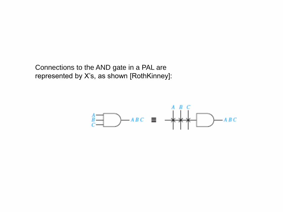
Connections to the AND gate in a PAL are
represented by X’s, as shown [RothKinney]:
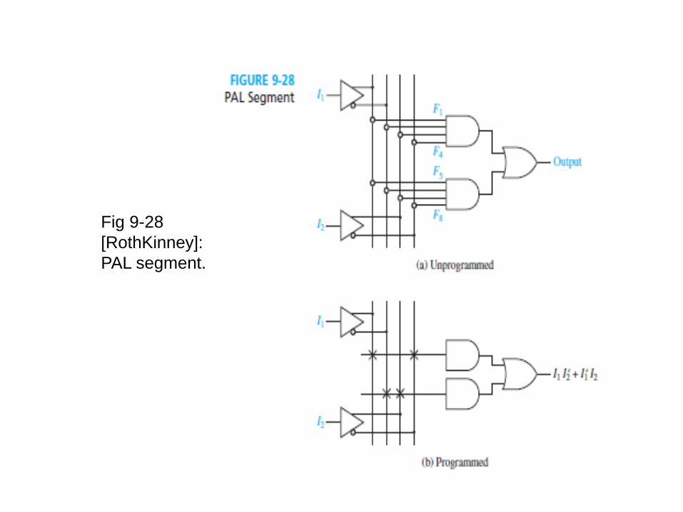
Fig 9-28
[RothKinney]:
PAL segment.
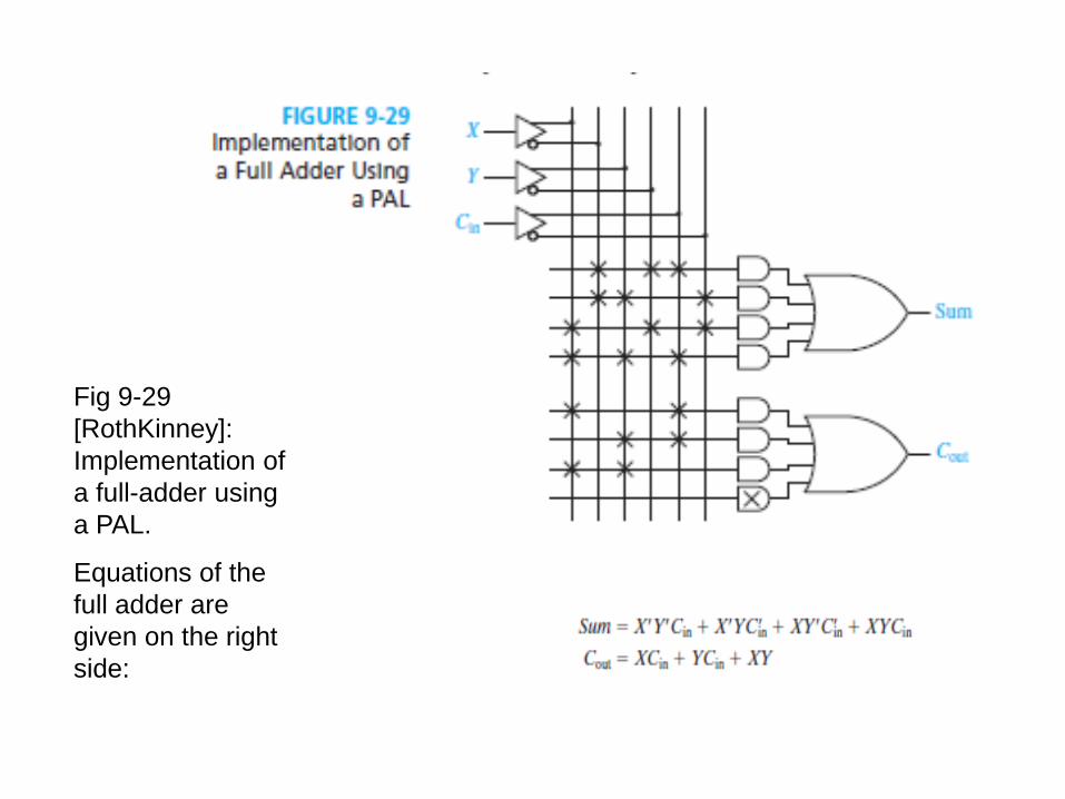
Fig 9-29
[RothKinney]:
Implementation of
a full-adder using
a PAL.
Equations of the
full adder are
given on the right
side:
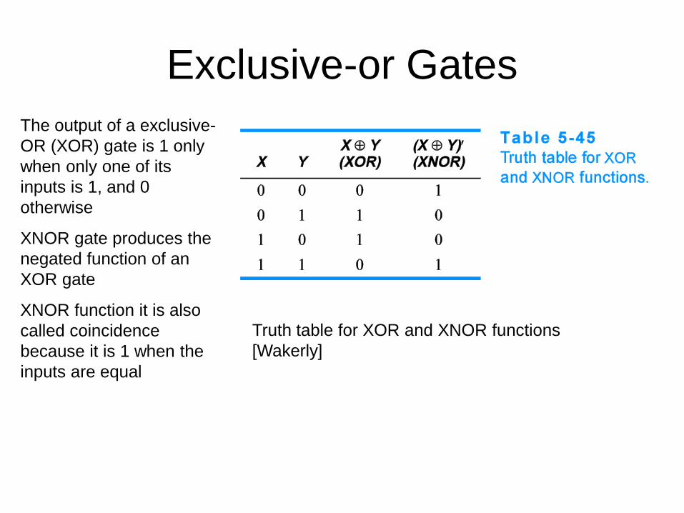
Exclusive-or Gates
Truth table for XOR and XNOR functions
[Wakerly]
The output of a exclusive-
OR (XOR) gate is 1 only
when only one of its
inputs is 1, and 0
otherwise
XNOR gate produces the
negated function of an
XOR gate
XNOR function it is also
called coincidence
because it is 1 when the
inputs are equal
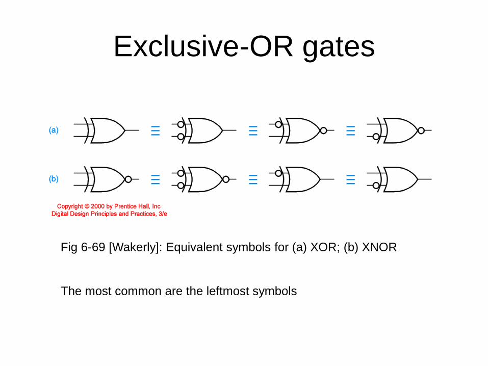
Exclusive-OR gates
Fig 6-69 [Wakerly]: Equivalent symbols for (a) XOR; (b) XNOR
The most common are the leftmost symbols
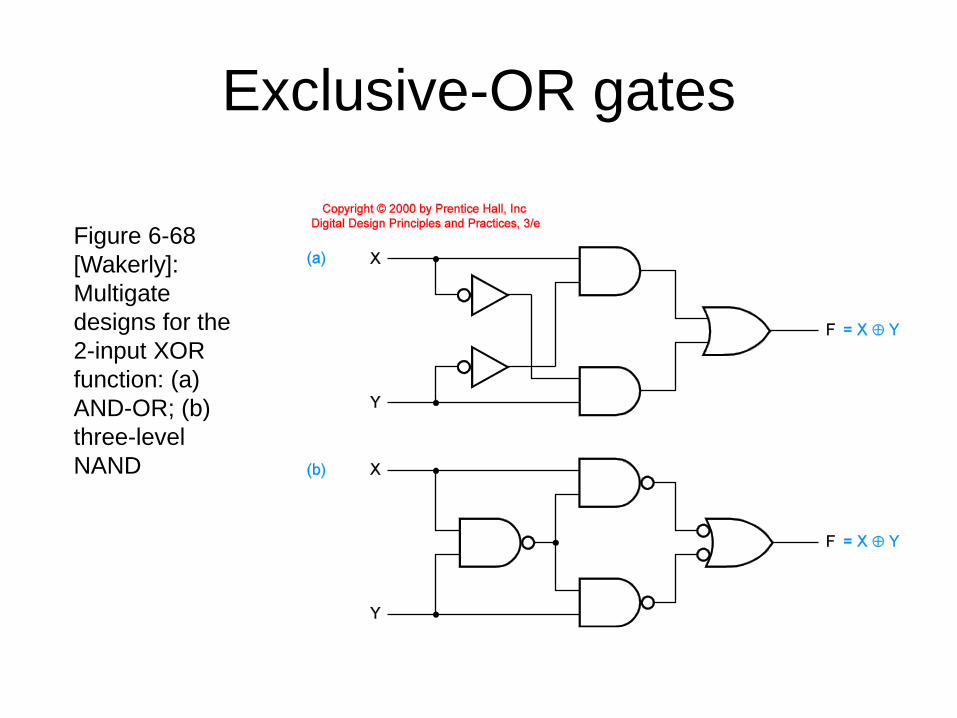
Exclusive-OR gates
Figure 6-68
[Wakerly]:
Multigate
designs for the
2-input XOR
function: (a)
AND-OR; (b)
three-level
NAND
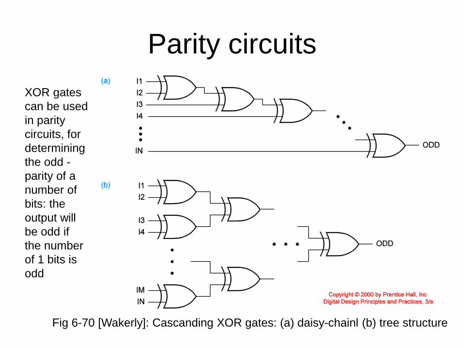
XOR gates
can be used
in parity
circuits, for
determining
the odd -
parity of a
number of
bits: the
output will
be odd if
the number
of 1 bits is
odd
Fig 6-70 [Wakerly]: Cascanding XOR gates: (a) daisy-chainl (b) tree structure
Parity circuits
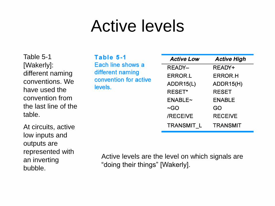
Active levels
Table 5-1
[Wakerly]:
different naming
conventions. We
have used the
convention from
the last line of the
table.
At circuits, active
low inputs and
outputs are
represented with
an inverting
bubble.
Active levels are the level on which signals are
“doing their things” [Wakerly].