classification of digital circuits
DESCRIPTION
Classification of Digital Circuits. Combinational logic circuits. Output depends only on present input. Sequential circuits. Output depends on present input and present state of the circuit. Combinational Logic Design Procedure. Start with the problem statement. - PowerPoint PPT PresentationTRANSCRIPT

Classification of Digital Circuits
• Combinational logic circuits.– Output depends only on present
input.• Sequential circuits.
– Output depends on present input and present state of the circuit.

Combinational Logic Design Procedure
• Start with the problem statement.• Determine the number of inputs
variables and the required number of output variables.
• Derive a truth table that defines the required relationship between input and output.
• Simplify each output function (Karnaugh maps).
• Draw the logic diagram.

Half Adder Design Example
• A half adder computes the sum of two one bit Boolean inputs, which can be at most 102. This requires two outputs.
• Inputs: X, and Y.Outputs: S and C.
X Y C S0 0 0 00 1 0 11 0 0 11 1 1 0

Half Adder Design Example
• C = XY• S = X Y

Decoders• A decoder is a multiple-input
multiple-output logic circuit that converts coded inputs into coded outputs, where the inputs and outputs codes are different.
Function Realization With Decoders
• The outputs of a binary decoder provides 2n minterms for its n inputs, and a Boolean functions can be represented as a sum of minterms, therefore a decoder and one or more OR gates can be used to realize sums of minterms of n variables.
Multiplexers• Combinational logic circuit
that selects binary information from one of many input lines and directs it to a single output line. The input is selected by the binary value on the select lines.

Demultiplexers• Combinational logic circuit
that receives binary information on a single input and sends this information to one of many possible output lines. The output is selected by the binary value on the select lines.

Function Realization With Multiplexers
• A multiplexer is basically a binary decoder whose outputs were ORed together and some extra input lines were added to each product term.
Function Realization With Multiplexers
• A sum of minterms can be realized by setting the corresponding input line of the chosen minterms to 1 and setting the input lines of the remaining minterms to 0.

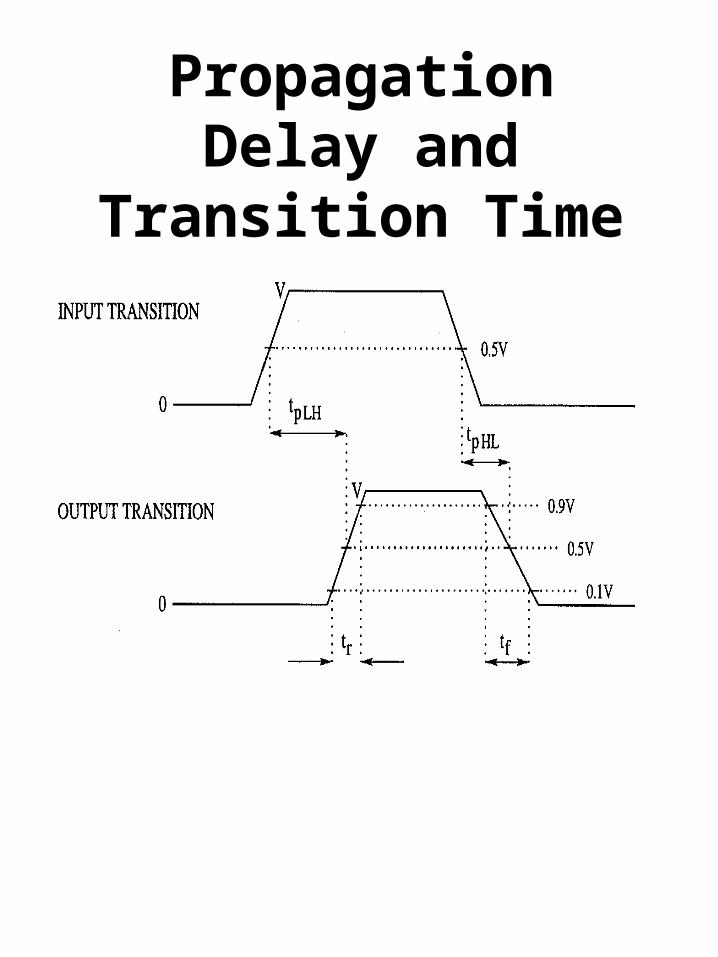
Transition Time• Time interval between two
reference points on a waveform. These reference points are usually 10% and 90% of the voltage change.– Rise time( tr ) – Time interval
when waveform is changing from a logic low to a logic high level.
– Fall time( tr ) – Time interval when waveform is changing from a logic high to a logic low level.
Propagation Delay• Time it takes for a change at
the input of a device to produce a change at the output of the same.– tpLH is the propagation delay
when the output changes from LOW to HIGH.
– tpHL is the propagation delay when the output changes from HIGH to LOW.
– tpLH and tpHL are not necessarily equal, and their values depends on the logic family.
Propagation Delay and Transition Time

Fanout• The number of gate inputs
that a single output can drive or operate without exceeding its worst case loading specifications.– IILMax is the maximum current
supplied by an input when a LOW logic level voltage is applied to that input.
– IIHMax is the maximum current required by an input when a HIGH logic level voltage is applied to that input.
– IOLMax is the maximum current into an output when this output is in the LOW state.
– IOHMax is the maximum current provided by an output when this output is in the HIGH state.

Fanout
Fanout
fanout HSfanout, LS min fanout
fanout HS
fanout LS
IH
OH
IL
OL
II
II

Power Dissipation• The power consumed by the
gate that must be available from the power supply. This does not include the power delivered from another gate.– VCC : supply voltage.– ICCH : current drawn by the
circuit when the output of the gate is HIGH.
– ICCL : current drawn by the circuit when the output of the gate is LOW.
– ICC : average current drawn by the circuit.
– PD : average power dissipation.
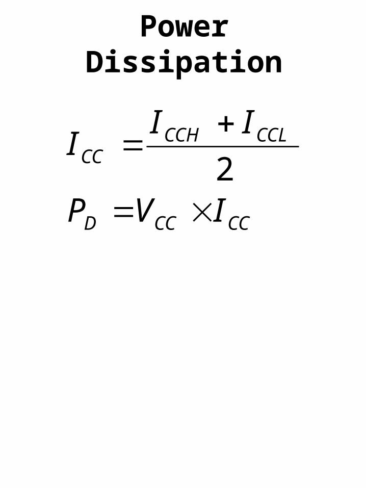
Power Dissipation
CCCCD
CCLCCHCC
IVP
III
2

DC Noise Margins• The maximum amount of
voltage variation (noise) that may be permitted for LOW or HIGH voltage levels.– VOHMin : the minimum output
voltage in the HIGH state.– VIHMin : the minimum input
voltage guaranteed to be recognized as a HIGH.
– VILMax : the maximum input voltage guaranteed to be recognized as a LOW.
– VOLMax : the maximum output voltage in the LOW state.
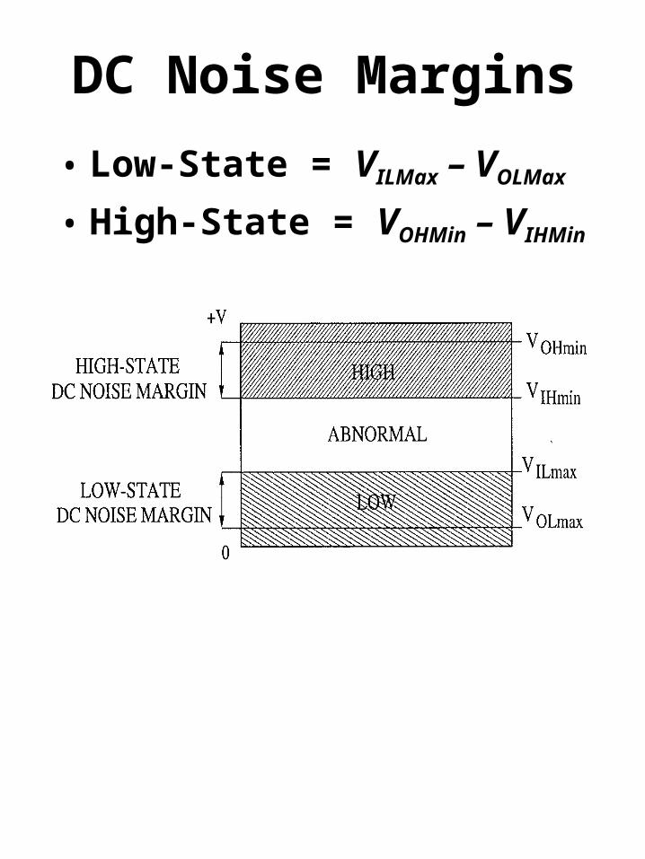
DC Noise Margins• Low-State = VILMax – VOLMax
• High-State = VOHMin – VIHMin

Unused Inputs• Handle them as follows:
– Tie them to a used input in the same gate.
– Tie them to logic 1 through a pull-up resistor for AND & NAND gates.
– Tie them to logic 0 through a pull-down resistor for OR & NOR gates.

Logic Families• Transistor Transistor Logic
(TTL) is one of the most popular and widespread of all logic families.– Very high number of SSI and
MSI devices available in the market.
– Several number of sub-families that provide a wide range of speed and power consumption.
• Sub families:– 74xx : The original TTL family.
• These devices had a propagation delay of 10ns and a power consumption of 10mW, and they were introduced in the early 60’s.

Logic Families• Sub families:
– 74Hxx : High speed.• Speed was improved by reducing
the internal resistors. Note that this improvement caused an increase in the power consumption.
– 74Lxx : Low power.• Power consumption was improved
by increasing the internal resistances, and the speed decreased.

Logic Families• Sub families:
– 74Sxx : Schottky.• The use of Schottky transistors
improved the speed. The power dissipation is less than the 74Hxx sub-family.
– 74LSxx : Low power Schottky.• Uses Schottky transistors to
improve speed. High internal resistances improves power consumption.
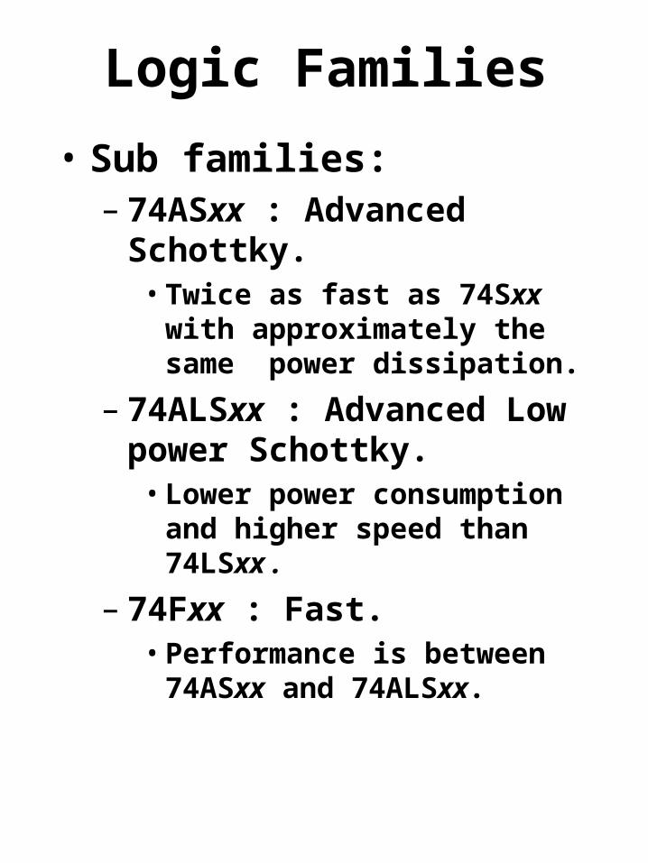
Logic Families• Sub families:
– 74ASxx : Advanced Schottky.• Twice as fast as 74Sxx with
approximately the same power dissipation.
– 74ALSxx : Advanced Low power Schottky.
• Lower power consumption and higher speed than 74LSxx .
– 74Fxx : Fast.• Performance is between 74ASxx
and 74ALSxx.

Logic Families• Note that parameters like
VOHMin , VIHMin , VILMax , and VOLMax are all the same for the different sub-families, but parameters like IILMax , IIHMax , IOLMax , and IOHMax may differ.
• Most TTL sub-families have a corresponding 54-series (military) version, and these series operate in a wider temperature and voltage ranges.
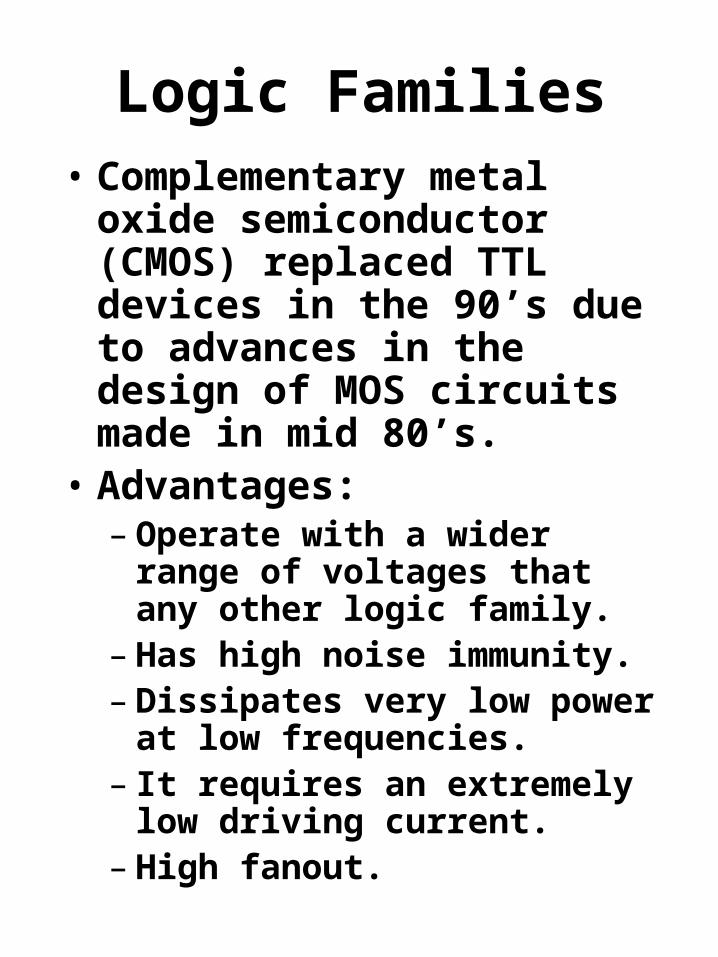
Logic Families• Complementary metal oxide
semiconductor (CMOS) replaced TTL devices in the 90’s due to advances in the design of MOS circuits made in mid 80’s.
• Advantages:– Operate with a wider range of
voltages that any other logic family.
– Has high noise immunity.– Dissipates very low power at
low frequencies.– It requires an extremely low
driving current.– High fanout.

Logic Families
• Disadvantages:– Power consumption increases
with frequency.– Susceptible to ESD - electro-
static discharges.• Sub-families:
– 40xx : Original CMOS family.• Fairly slow, but it has a low power
dissipation.– 74HCxx : High speed CMOS.
• Better current sinking and sourcing than 40xx. It uses voltage supply between 2 and 6 volts.
• Higher voltage →higher speed.• Lower voltage →lower power
consumption.

Logic Families• Sub-families:
– 74HCTxx : High speed CMOS, TTL compatible.
• Better current sinking and sourcing than 40xx. It uses voltage supply of 5V. Compatible with TTL family.
– 74ACxx : Advanced CMOS.• Very fast. It can source and sink
high currents. Not TTL compatible.
– 74ACTxx : Advanced CMOS, TTL compatible.
• Same as 74ACxx, but it is compatible with TTL family.

Logic Families• Sub-families:
– 74FCTxx : Fast CMOS, TTL compatible.
• It is faster and has lower power dissipation than the 74ACxx and 74ACTxx sub-families. Compatible with TTL family.
• Prefixes, usually added to device designation to identify the manufacturer.– SN : Texas Instrument.– MN : Motorola.– DM : National– N : Signetics– P : Intel– H : Harris– AMD : Advanced Micro Devices

Logic Families• Prefixes, usually added to device
designation to identify the manufacturer.– SN : Texas Instrument.– MN : Motorola.– DM : National– N : Signetics– P : Intel– H : Harris– AMD : Advanced Micro Devices
• Suffixes, identifies the packaging.– N : Plastic DIP (dual in-line package)– P : Plastic DIP– J : Ceramic DIP– W : Ceramic flat package.– D : Plastic ‘small outline’ package

Latches andFlip-Flops
• These sequential devices differ in the way their outputs are changed:– The output of a latch changes
independent of a clocking signal.
– The output of a flip–flop changes at specific times determined by a clocking signal.

S-R Latch• SR latch based on NOR gates.• The S input sets the Q output
to 1 while R reset it to 0.• When R=S=0 then the output
keeps the previous value.• When R=S=1 then Q=Q’=0,
and the latch may go to an unpredictable next state.
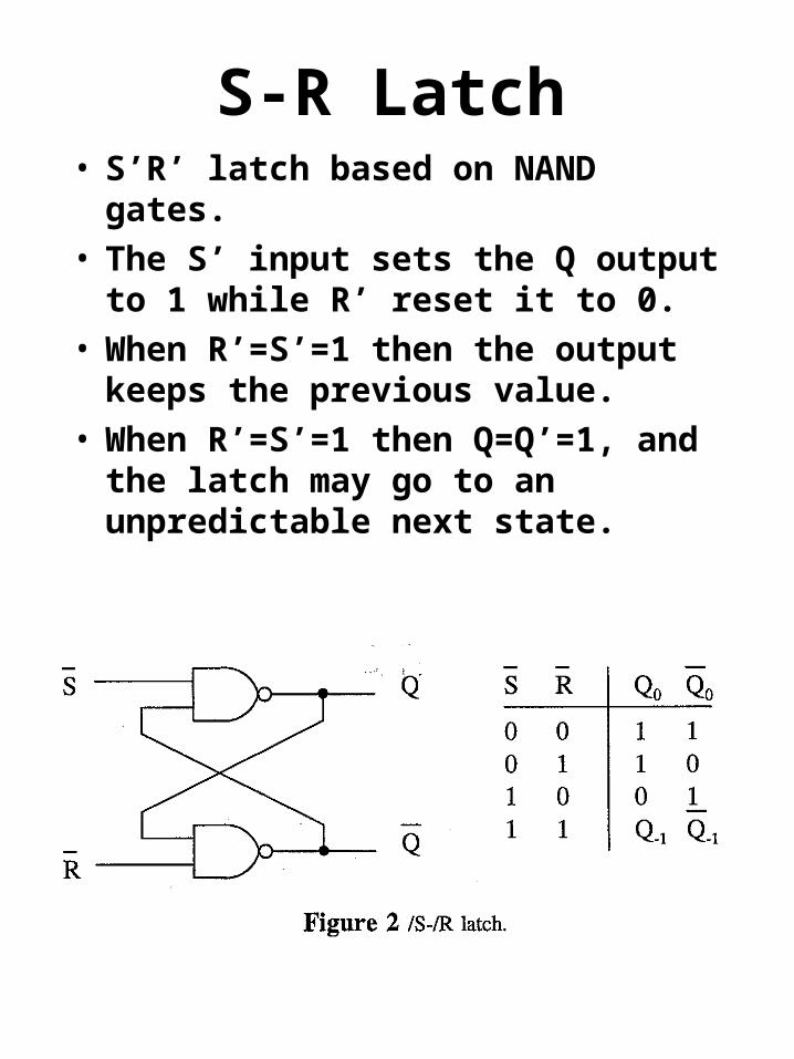
S-R Latch• S’R’ latch based on NAND gates.• The S’ input sets the Q output to 1
while R’ reset it to 0.• When R’=S’=1 then the output
keeps the previous value.• When R’=S’=1 then Q=Q’=1, and
the latch may go to an unpredictable next state.

D Latch• This latch eliminates the
problem that occurs in the S’R’ latch when R=S=0.
• C is an enable input:– When C=1 then the output
follows the input D and the latch is said to be open.
– When C=0 then the output retains its last value and the latch is said to be closed.

D Latch• For proper operation the D
input must not change during a time interval around the falling edge of C.
• This time interval is defined by the setup time – tsetup and the hold time – thold .
Edge Triggered DFlip-Flop
• This flip-flop is made out of two D latches. The first latch is the master, and the second the slave.
• When Ck = 0 the master is open and the slave is closed. Qm and Ds follow Dm .
• When Ck = 1 the master is closed, the slave is open and Qm is transferred to Qs . Note that Qs does not change because the master latch is closed leaving Qm fixed.

Edge Triggered DFlip-Flop
• The same constraints regarding setup and hold time discussed previously, also apply to the edge triggered D flip-flop.

Edge Triggered J-KFlip-Flop
• The operation of inputs J and K in the J-K flip-flop is similar to the operation of inputs S and R in the S-R flip-flop. The difference arises when J and K are asserted simultaneously. In this situation the output of the J-K flip-flop inverts its current state.

T Flip-Flop
• Also known as the toggle flip-flop.
• When input T = 0 the output Q retain its previous value.
• When input T = 1 the output Q inverts on every tick of the clock.
• When inputs J and K of a J-K flip-flop are connected together, the J-K flip-flop will behave like a T flip-flop.

Sequential Logic Design Procedure
• Derive a state/output table from the problem specification.
• Minimize the number of states in the state/output table by eliminating equivalent states.
• Choose a set of state variables. Assign to each state a unique combination from the set derived above.
• Create a transition/output table.
Sequential Logic Design Procedure
• Choose a flip-flop type and construct its excitation table.
• Using the excitation table fill the values for the input excitation function columns on the transition/output table.
• Derive the excitation and output equations.
• Draw logic diagram.

Sequence Detector Design Example
• Design a sequential circuit with one input ( I ) and one output ( Z )The output is asserted when the input sequence 0-1-1 is received.
• See state/output table below.
Input OutputI Z0 S 0 01 Init 00 S 0 01 S 01 00 S 0 01 S 011 00 S 011 11 S 011 1
S 01
S 011
Present State Next stateInit
S 0

Sequence Detector Design Example
• Set of state variables and their unique assignment to the different states.
State Q1 Q0Init 0 0S 0 0 1S 01 1 1S 011 1 0
Sequence Detector Design Example
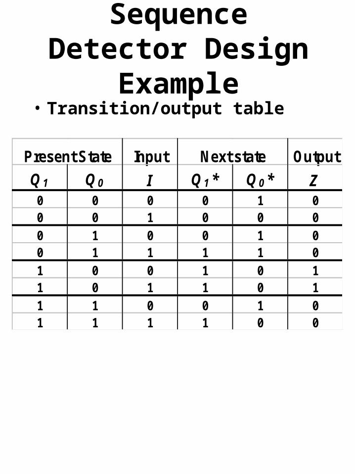
• Transition/output table
Input OutputQ 1 Q 0 I Q 1 * Q 0 * Z
0 0 0 0 1 00 0 1 0 0 00 1 0 0 1 00 1 1 1 1 01 0 0 1 0 11 0 1 1 0 11 1 0 0 1 01 1 1 1 0 0
Present State Next state

Sequence Detector Design Example
• See excitation table below.
D J K T0 0 0 0 X 00 1 1 1 X 11 0 0 X 1 11 1 1 X 0 0
Present State Next StateRequired inputs

Sequence Detector Design Example
Input OutputQ 1 Q 0 I Q 1 * Q 0 * Z J 1 K 1 J 0 K 0
0 0 0 0 1 0 0 X 1 X0 0 1 0 0 0 0 X 0 X0 1 0 0 1 0 0 X X 00 1 1 1 1 0 1 X X 01 0 0 1 0 1 X 0 0 X1 0 1 1 0 1 X 0 0 X1 1 0 0 1 0 X 1 X 01 1 1 1 0 0 X 0 X 1
Present State Next state Input Excitation
• Equations derived from the table above:– J1 = IQ0
– K1 = I’Q0
– J0 = I’Q1‘– K0 = IQ1
– Z = Q1Q0’

Sequence Detector Design Example
• See the logic diagram for the circuit below.
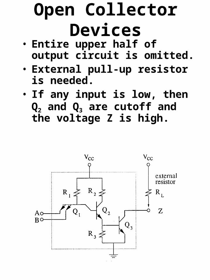
Open Collector Devices• Entire upper half of output circuit
is omitted.• External pull-up resistor is
needed.• If any input is low, then Q2 and Q3
are cutoff and the voltage Z is high.

Open Collector Devices• Can be used to drive a load, such
as LEDs, relays or other device.• It is important to calculate a
suitable resistor R.• The current through the load must
not exceed IOLMax .
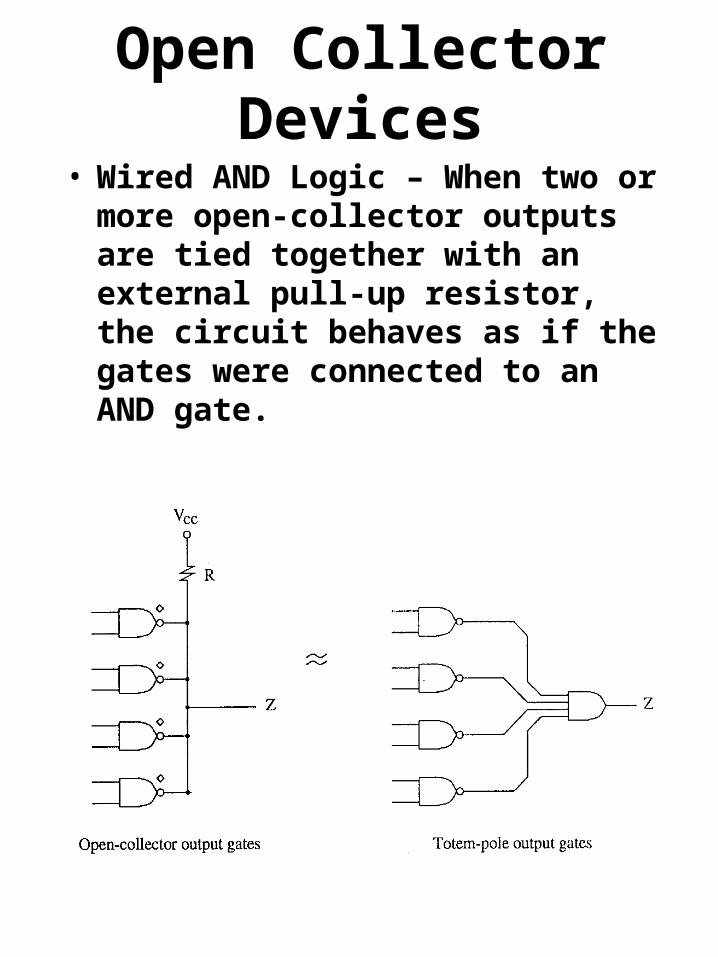
Open Collector Devices• Wired AND Logic – When two or
more open-collector outputs are tied together with an external pull-up resistor, the circuit behaves as if the gates were connected to an AND gate.

Open Collector Devices• Common Bus – Several open collector
outputs may be connected together to create a common bus.
• The decoder, in the circuit shown below, selects which device outputs to the common bus by sending a high to the open collector output NAND gate connected to the chosen device.

Open Collector Devices• To calculate the pull-up
resistor of the figure in the next two pages, one must consider two cases:– Only one gate is active and
forces the bus voltage to be LOW, VOLTyp .
– All gates are disabled forcing the bus voltage to be HIGH, VOHMin .
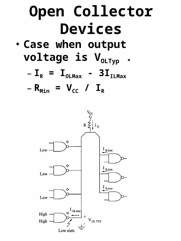
Open Collector Devices• Case when output voltage is
VOLTyp .– IR = IOLMax - 3IILMax
– RMin = VCC / IR
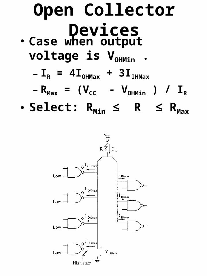
Open Collector Devices• Case when output voltage is
VOHMin .– IR = 4IOHMax + 3IIHMax
– RMax = (VCC - VOHMin ) / IR
• Select: RMin ≤ R ≤ RMax

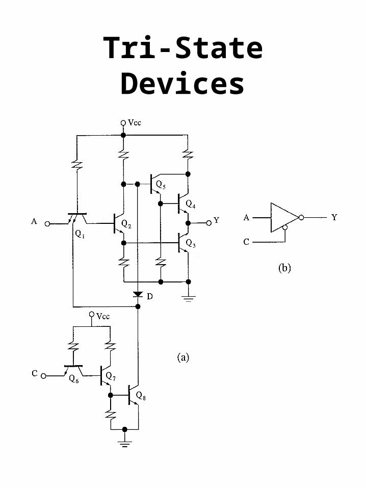
Tri-State Devices • This kind of device include a third
electrical state called high impedance or Hi-Z.
• This new state is controlled by an input control line called output enable. When this input is asserted the device behaves like a normal gate, otherwise, the output behaves like an open circuit.
C' A Y0 0 10 1 01 0 Hi-Z1 1 Hi-Z
Tri-State Devices
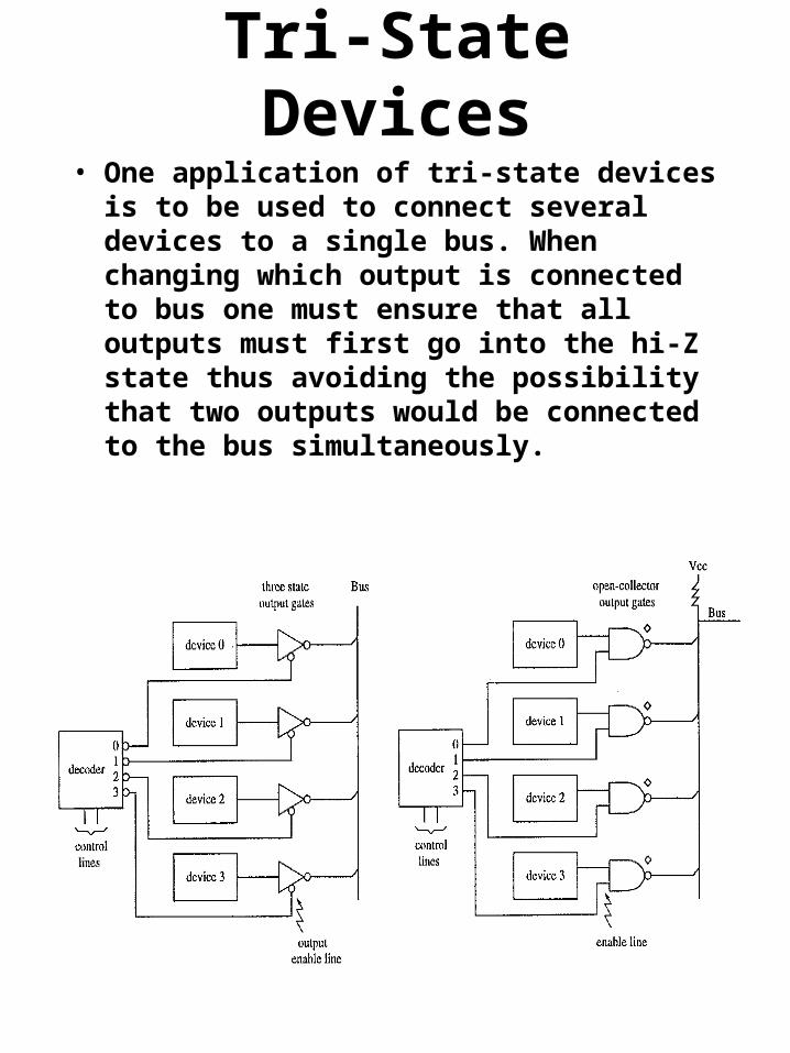
Tri-State Devices• One application of tri-state devices is to
be used to connect several devices to a single bus. When changing which output is connected to bus one must ensure that all outputs must first go into the hi-Z state thus avoiding the possibility that two outputs would be connected to the bus simultaneously.
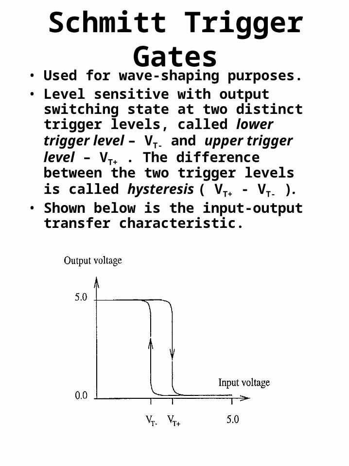
Schmitt Trigger Gates• Used for wave-shaping purposes.• Level sensitive with output switching
state at two distinct trigger levels, called lower trigger level – VT- and upper trigger level – VT+ . The difference between the two trigger levels is called hysteresis ( VT+ - VT- ).
• Shown below is the input-output transfer characteristic.
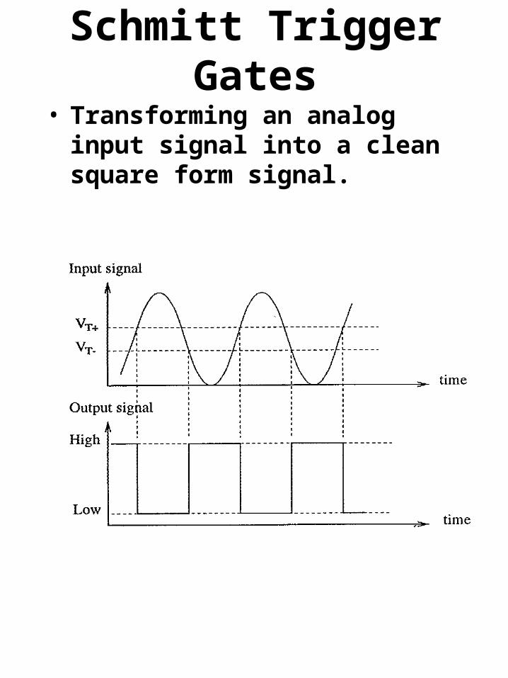
Schmitt Trigger Gates• Transforming an analog input
signal into a clean square form signal.