chapter 5 steady state analysis and simulation of the …
TRANSCRIPT

106CHAPTER 5
STEADY STATE ANALYSIS AND SIMULATION OF THE IPM GENERATOR
FEEDING A RECTIFIER-BUCK-RESISTIVE LOAD
5.1 Introduction
In this chapter, the steady state analysis and simulation of the IPM generator feeding
a rectifier-buck resistive load will be presented. The first part of the chapter concerns itself
with developing mathematical equations which describe the switching functions of the buck
converter for steady state. An equivalent resistance which is dependent upon the actual load
resistance and the duty cycle of the converter will be obtained. In addition, various plots
showing how an ideal voltage source system feeding a buck system behaves will be
generated. The graphs are useful in conceptualizing how the buck converter works.
Next, using the mathematical model developed, the steady state experimental results
will be compared with the predicted results. The method used to model the transistor and
the control signal to turn it on and off will be presented and a comparison between the
measured and simulated waveforms will be given.
The normal goal of dc-dc converters is to maintain a desired output voltage
at a desired level, even though the input voltage and the output load may vary. Figure 5.1
shows a simple example of a dc-dc converter where the average output voltage is controlled
by the switch on and off times (DT and (1-D) T). D is the duty ratio (cycle) and is defined
as the ratio of the on- duration to the total switching time period T.

107
Figure 5.1. Basic dc-dc converter and associated voltage output
If the switch is always on, it is easy to see that the average output voltage will equal
the input voltage; however, as the percentage of time that the switch is off increases, the
average output voltage will decrease and will obviously become equal to zero when the
switch is always off. The scheme thus far described is a buck converter (which has the
ability to regulate the output voltage from a maximum value equal to the supply voltage to a
minimum value equal to zero volts); however, it can be seen that while one is able to control
the average value of the output voltage, the instantaneous voltage fluctuates between zero
and V1 . This fluctuation is not acceptable in most of the applications where a regulated dc
supply voltage is required.
The problem of output voltage fluctuation is largely solved by using a low pass filter
consisting of a series inductor and a parallel capacitor. Figure 5.2 shows the schematic of
the basic dc-dc converter with the low pass filter in place. It can also be seen that a diode
(1-D)T
DT V1
<V2>V1
+
--
t

108
Figure 5.2. Dc-dc (buck) converter with low pass filter
has also been included in the circuit. Its presence is primarily needed to prevent the switch
(transistor) from having to dissipate or absorb inductive energy ( which would destroy it).
The low pass filter components are chosen so that the corner frequency is much
lower than the switching frequency of the switch itself. When this is done, the output
voltage fluctuation is virtually eliminated and for most analyses, the output voltage can be
assumed to be a constant dc voltage [34].
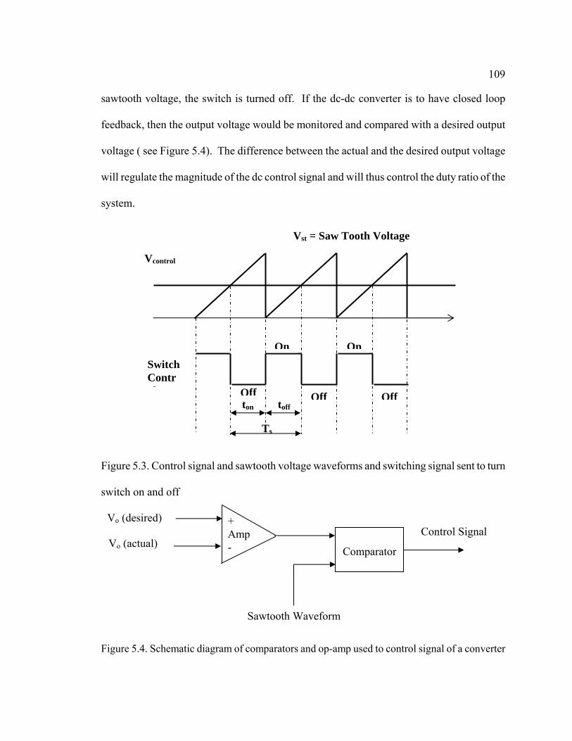
Thus far, the way in which the switch is turned on and off has not been discussed.
The regulation of the output voltage is achieved via a pulse width modulator which controls
how long a switch is on and off. Figure 5.3 shows a saw tooth voltage and dc control voltage
plotted vs time. When the dc voltage is larger than the saw tooth voltage, the switch is
turned on, and when the voltage becomes smaller than the
109
sawtooth voltage, the switch is turned off. If the dc-dc converter is to have closed loop
feedback, then the output voltage would be monitored and compared with a desired output
voltage ( see Figure 5.4). The difference between the actual and the desired output voltage
will regulate the magnitude of the dc control signal and will thus control the duty ratio of the
system.
Figure 5.3. Control signal and sawtooth voltage waveforms and switching signal sent to turn
switch on and off
Figure 5.4. Schematic diagram of comparators and op-amp used to control signal of a converter
Ts
Vst = Saw Tooth Voltage
ton
Offtoff
Vcontrol
Switch Contrl
On On
Off Off
+ Amp-
Comparator
Vo (desired)
Vo (actual) Control Signal
Sawtooth Waveform

110
5.2 Derivation of a Buck Converter Operating in Steady State
The derivation for the steady state equivalent circuit of a buck converter builds upon
the result found for the equivalent circuit which represents the rectifier feeding a resistive
load. Figure 5.5 shows the current flowing through the inductor Lp (see Figure 5.6) along
with the switching functions associated with the three modes of operation for the buck
converter. The first mode is when the transistor T1 is on, the second is when T1 is off and
the current flowing through the inductor Lp is greater than zero, and the third mode is when
the transistor T1 is off and the current flowing through the inductor Lp is zero.
Figure 5.5. Inductor current and switching functions for the buck converter

111
Figure 5.6. Schematic diagram of an IPM generator feeding a rectifier-buck-resistive load
Figure 5.7 Buck converter in mode 1 operation
Figure 5.8. Buck converter in modes 2 and 3
Ld
Vs Vc1 Vco
Lp
C1 Co RL
Ip I1
Ld
Vs Vc1 Vco
Lp
C1 Co RL
Ip I1

112
Before beginning the derivation for the buck converter, the mathematical basis for the
fundamental approximation in the state-space averaging approach will be given. The
derivation is taken from [35].
Let two linear systems described by
(i) Interval Td1 , 0 < t <to :
(ii) Interval Td2 , to < t <T:
The exact solution of the state-space equations are
Across the switching instant to the state-variable vector x(t) is continuous, and,
therefore
A linear approximation of the solution of the system can be accomplished by using
the Baker-Campbell-Hausdorff series
,x A = x 1& (5.1)
. x A = x 2& (5.2)
.T] ,t[ t x(o) e = x(t)]t[0, t x(o) e = x(t)
o)t-(tA
otA
o2
1
∈
∈ (5.3)
. x(0)ee = )tx( e = x(T) T AdT A do
)Td-(T A 112212 (5.4)
,T )A A - A A( d d + T )A d + A d( = AT 21221212211 (5.5)

113
where
The first approximation solutions are
where I is the identity matrix.
Therefore,
which results in the approximate solution
This is the same as the solution of the following linear system equation for x(T):
This equation is the averaged model obtained from the switched models given in
Equations (5.1 ) and (5.2) .
. e e = e T A dT A dT A 1122
,T A d + I e
T A d + I e22
T A d
11T A d
22
11
≈
≈ (5.6)
e ee ,T )A d + A d(T A dT A d 22111122 ≈ (5.7)
. x(0) e x(T) T )A d + A d( 2211≈ (5.8)
. x )A d + A d( = x 2211& (5.9)
114
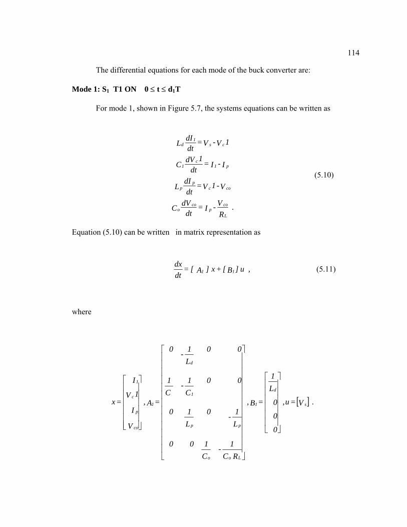
The differential equations for each mode of the buck converter are:
Mode 1: S1 T1 ON 0 ≤ t ≤ d1T
For mode 1, shown in Figure 5.7, the systems equations can be written as
Equation (5.10) can be written in matrix representation as
where
. RV - I =
dtdVC
V - 1V = dt
dIL
I- I = dt
1dVC
1V - V = dtdIL
L
cop
coo
cocp
p
p1c
1
cs1
d
(5.10)
u ,] B[ + x] A [ = dtdx
11 (5.11)
[ ] . V =u ,
0
0
0
L1
= B ,
R C1-
C100
L1-0
L10
00C1-
C1
00L1-0
= A ,
V
I
1V
I
= x s
d
1
Loo
pp
1
d
1
co
p
c
1
⎥⎥⎥⎥⎥⎥
⎦
⎤
⎢⎢⎢⎢⎢⎢
⎣
⎡
⎥⎥⎥⎥⎥⎥⎥⎥⎥⎥⎥⎥⎥
⎦
⎤
⎢⎢⎢⎢⎢⎢⎢⎢⎢⎢⎢⎢⎢
⎣
⎡
⎥⎥⎥⎥⎥⎥
⎦
⎤
⎢⎢⎢⎢⎢⎢
⎣
⎡

115
Mode 2: S2 T1 OFF ( Ip >0) d1T ≤ t ≤ d2T
For mode 2, shown in Figure 5.8, the systems equations can be written as
For mode 2, shown in Figure 5.8, the systems equations can be written as
where
u ,] B[ + x] A [ = dtdx
22 (5.13)
. RV- I =
dtdVC
V- = dt
dIL
I = dt
1dVC
1V - V = dtdIL
L
cop
coo
cop
p
1c
1
cs1
d
(5.12)
[ ] . V =u ,
0
0
0
L1
= B ,
R C1-
C100
L1-000
000 C1
00L1-0
= A ,
V
I
1V
I
= x s
d
2
Loo
p
1
d
2
co
p
c
1
⎥⎥⎥⎥⎥⎥
⎦
⎤
⎢⎢⎢⎢⎢⎢
⎣
⎡
⎥⎥⎥⎥⎥⎥⎥⎥⎥⎥⎥⎥⎥
⎦
⎤
⎢⎢⎢⎢⎢⎢⎢⎢⎢⎢⎢⎢⎢
⎣
⎡
⎥⎥⎥⎥⎥⎥
⎦
⎤
⎢⎢⎢⎢⎢⎢
⎣
⎡

116
Mode 3: S3 T1 OFF ( Ip =0) (d1 + d2 )T ≤ t ≤ (d1 +d2 +d3 )T
For mode 3, (shown in Figure 5.8) with the understanding that the current in the
inductor Lp = 0, the systems equations can be written as
The same differential equations written in matrix representation are
where
. RV- =
dtdVC
0 = dt
dIL
I = dt
1dVC
1V - V = dtdIL
L
cocoo
pp
1c
1
cs1
d
(5.14)
u ,] B[ + x] A [ = dtdx
33 (5.15)
[ ] . V =u ,
0
0
0
L1
= B ,
R C1-000
0000
000 C1
00L1-0
= A ,
V
I
1V
I
= x s
d
3
Lo
1
d
3
co
p
c
1
⎥⎥⎥⎥⎥⎥
⎦
⎤
⎢⎢⎢⎢⎢⎢
⎣
⎡
⎥⎥⎥⎥⎥⎥⎥⎥⎥⎥⎥
⎦
⎤
⎢⎢⎢⎢⎢⎢⎢⎢⎢⎢⎢
⎣
⎡
⎥⎥⎥⎥⎥⎥
⎦
⎤
⎢⎢⎢⎢⎢⎢
⎣
⎡
117
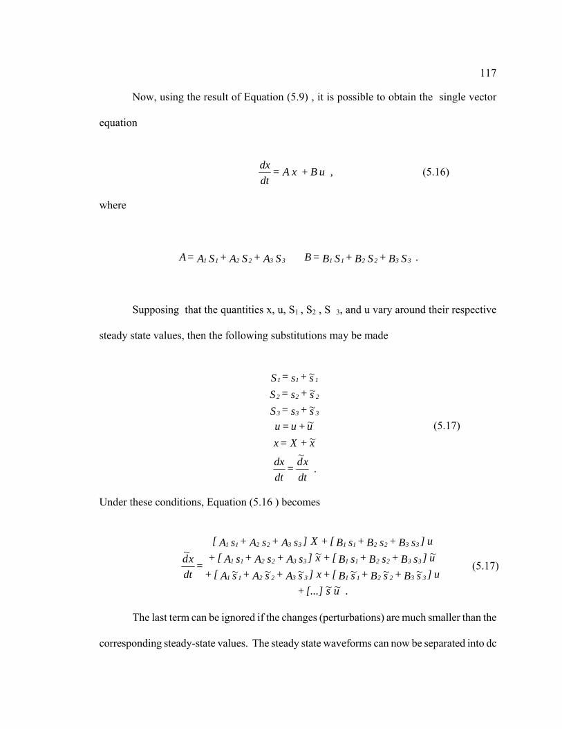
Now, using the result of Equation (5.9) , it is possible to obtain the single vector
equation
where
Supposing that the quantities x, u, S1 , S2 , S 3, and u vary around their respective
steady state values, then the following substitutions may be made
Under these conditions, Equation (5.16 ) becomes
The last term can be ignored if the changes (perturbations) are much smaller than the
corresponding steady-state values. The steady state waveforms can now be separated into dc
u , B + x A = dtdx (5.16)
. S B + S B + S B = B S A + S A + S A = A 332211332211
. dtxd =
dtdx
x + X = xu +u =u s + s = Ss + s = Ss + s = S
333
222
111
~~~~~~
(5.17)
. u s[...] +u] s B + s B + s B[ + x] s A + s A + s A[ +
u] s B + s B + s B[ + x] s A + s A + s A[ +u] s B + s B + s B[ + X] s A + s A + s A[
= dtxd
332211332211
332211332211
332211332211
~~~~~~~~
~~~ (5.17)

118
and ac components. Of interest here is the dc component which is given as
The dc ( average value) of the switching functions are
and, recognizing that
then d3 may be written as
. d - d -1 = d 213 (5.21)
Substituting Equation (5.21 ) into (5.18 ) and rearranging gives
. 0 = u] s B + s B + s B[ + X] s A + s A + s A[ 332211332211
,d = T
T d = s
d = T
T d = s
d = T
T d = s
33
3
22
2
11
1
(5.19)
,1 = d + d + d 321 (5.20)

119
The effective input resistance is defined as the input voltage over the input current,
i.e.
In terms of the duty cycle and the load resistance RL the effective resistance can be found as
follows:
In terms of d1 and d3, Equation (5.24) may be written as
Referring to Figure 5.5, and assuming that the converter is operating in discontinuous
conduction mode (meaning that the current in the inductor becomes zero for a time) then,
. I )d + d( = RV
V d
)d+ d( = 1V
I d = I1V = V
p21L
co
co1
21c
p11
cs
(5.22)
. IV = R
1
seff (5.23)
. R d
) d + d( = )I d
1( )d + d( I R d
d + d = Id
V = IV = R L2
1
221
p121PL
1
21
p1
s
1
seff (5.24)
. R d
)d - (1 = R L21
32
eff (5.25)

120
when the buck converter is operating in mode one, the current ip (t) rises linearly from a zero
value at the beginning of the mode to a maximum value at time t=d1T of
The converter will then switch into mode two operation and the current will fall
linearly from Ipmax to a zero value at a time t=(d1 + d2 )T. The average value of the inductor
current Ip over a complete cycle may be found by taking the area under the two triangles,
and dividing by the total time T. Thus,
At steady state, the average current in the capacitor C0 is zero. Since this is true, then
the average current going into the load resistance RL must equal the average current in the
inductor Lp . Thus,
or
. L
T d )V - 1V( = Ip
1cocpmax (5.26)
. L 2
) d + d( T d )V - 1V( = T 2
T) d + T d( I = Ip
211coc
21pmaxp (5.27)
,L 2
) d + d( T d )V - 1V( = RV = I
p
211coc
L
coL (5.28)
. L 2
) d + d( T d )V - 1V( R = Vp
211cocLco (5.29)

121
Substituting the value of Vc1 in Equation (5.22) gives
,L 2
) d + d( T d 1) - d
d+ d( V R = Vp
211
1
21coLco (5.30)
which, after simplification yields
In terms of d1 and d3 this equation becomes
Therefore, knowing the duty cycle d1 , the total period T, the load resistance RL , and
the value of the inductor Lp , the percentage of time that the converter is operating in
discontinuous conduction mode may be determined by solving Equation (5.31-b) for d3 . If
the solution for d3 is either zero or negative, then the converter is always in continuous
conduction mode.
For a given load resistance and period, the converter will tend toward discontinuous
conduction mode as both d1 and Lp are decreased. At the boundary condition between
continuous and discontinuous conduction mode, d3 =0, and Equation (5.31-b) may be written
as
. 0 = T RL 2
- d+ d dL
p222
21 (5.31-a)
. 0 = )R TL 2
- d 2 - d-(1 + 2) - d( d + dL
p1
2113
23 (5.31-b)

122
It can be seen that, as the duty cycle d1 is decreased, the inductor value must be
increased to satisfy the equation. As d1 tends toward zero then the equation may be
approximated as
Solving for Lp gives
Thus, if one wants to be sure of operating in continuous mode ( which is normally the
case because of the high stresses placed on the transistors when operating in discontinuous
mode ) regardless of the duty cycle, then a good rule of thumb to ensure this is to choose an
inductor value such that
For the steady state analysis in this thesis, only the continuous conduction mode was
considered. With that being the case, d3 of Equation (5.25) is zero and the effective
. R TL 2
= d 2 - d-1 L
p1
21 (5.32)
. R TL 2
= 1 L
p (5.33)
. 2R T = L L
p
. 2R T L L
p f (5.35)

123
resistance for the buck may be written as
The equivalent resistance given in Equation (5.36) may be substituted into Equation
(4.31) to obtain the equivalent resistance of the buck-rectifier system. After the substitution,
the equivalent resistance that the IPM (or any other power source) sees at its terminals is
given in Equation (5.37) and will be used to predict the performance of the IPM feeding a
rectifier-buck-resistance load.
. dR = R 2
1
Leffbk (5.36)
d 12 R = R 2
1
2L
effbkrecπ (5.37)

124
5.2.1 Examination of Ideal Buck Converter
In order to gain an appreciation of the significance of Equation 5.36, various graphs
are generated with the assumption that the dc voltage into the buck converter is a constant 10
volts dc, and the load resistance is a constant 10 ohms.
Figure 5.9. Effective resistance vs duty cycle for buck converter

125
Figure 5.9 displays how the effective resistance presented to the source decreases as
the duty cycle increases. This trend is the same as that of the boost converter except for the
fact that the buck effective resistance starts at an infinite resistance at a zero duty cycle and
ends at the value of the load resistance, and the boost starts at the value of the load resistance
and ends at a zero effective resistance.
Figure 5.10. Source (input) current vs duty cycle for buck converter
126
Figure 5.10 shows how the source current increases as the duty cycle increases. At a
duty cycle of zero the effective resistance is infinity and no current flows in the circuit. As
the duty cycle increases, the source current increases exponentially, but only up a maximum
value of Vdc/RL.
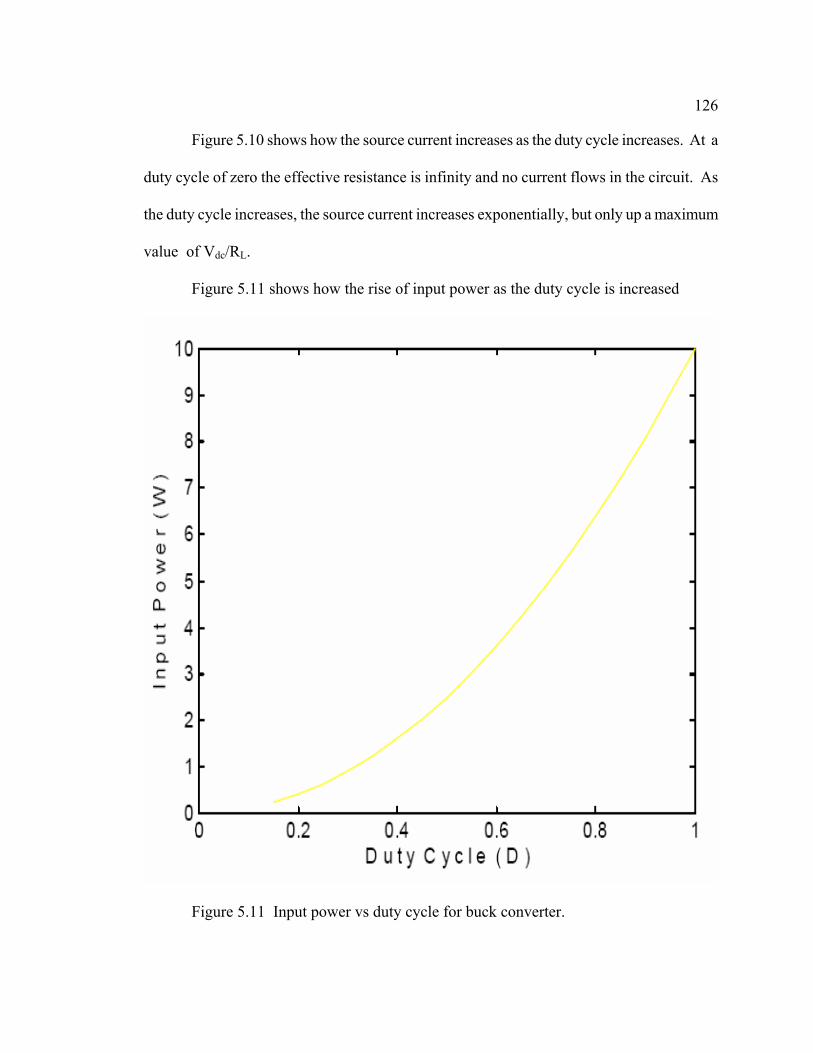
Figure 5.11 shows how the rise of input power as the duty cycle is increased
Figure 5.11 Input power vs duty cycle for buck converter.

127
Figure 5.12. Load voltage vs duty cycle for buck converter
Figure 5.12 displays the intended effect of the buck converter topology. As the duty cycle
is decreased, the load voltage becomes smaller than the source voltage. One point of interest
is that unlike the boost converter (which, as will be seen in the next chapter, is a function of
the duty cycle squared) the load voltage for the buck varies linearly with the duty cycle.
0 0.2 0.4 0.6 0.8 11
2
3
4
5
6
7
8
9
10
D u t y C y c l e ( D )
L o
a d
V o
l t a
g e
( V
d c
)

128
5.3 Steady State Performance of an IPM Generator Feeding a
Rectifier-Buck-Resistive Load
5.3.1 Introduction
In this section, the measured steady state performance of the IPM generator feeding a
rectifier-buck-resistive load will be compared with the predicted performance of the system.
In order to obtain a full performance curve (meaning that the performance of the IPM
generator is tested for loads ranging from a light load to a large load) for the buck
converter, it is not the load resistance RL which is varied from a small to a large value.
Rather, it is the duty cycle D which is varied from almost zero to 1.
Referring back to Figure 5.9, and remembering that the actual load resistance for
this graph was 10 ohms, it can be seen that the smallest resistance which the generator will
see is the actual load resistance RL. Thus, if one wants to be able to study the buck system
operating under a large load, a small load resistance must be chosen. As the duty cycle is
decreased from 1, the effective resistance increases and, therefore, it is possible to test the
topology under the condition when the IPM generator is feeding a small load.
The load resistance chosen to test the system was 2.5 Ω and the system was tested for
the operating frequencies of 30 and 45 Hz. The values of the rectifier filter components were
Ld = 9.3 mH and C1 = 10mF. The values of the buck filter were Lp = 10 mH and Co = 10mF.

129
5.3.2 Experimental and Predicted Performance Results Figure 5.13 shows how measured and calculated line to neutral voltage of the
generator varies as a function of the power out of the generator. If the rectifier-buck system
truly appeared as a purely resistive load to the IPM, then the measured results would fall
almost exactly on the calculated results line as they did in Figure 3.5.
Figure 5.13. Measured and calculated generator line to neutral voltage vs generator output
power for the IPM feeding a rectifier-buck-resistive load
130
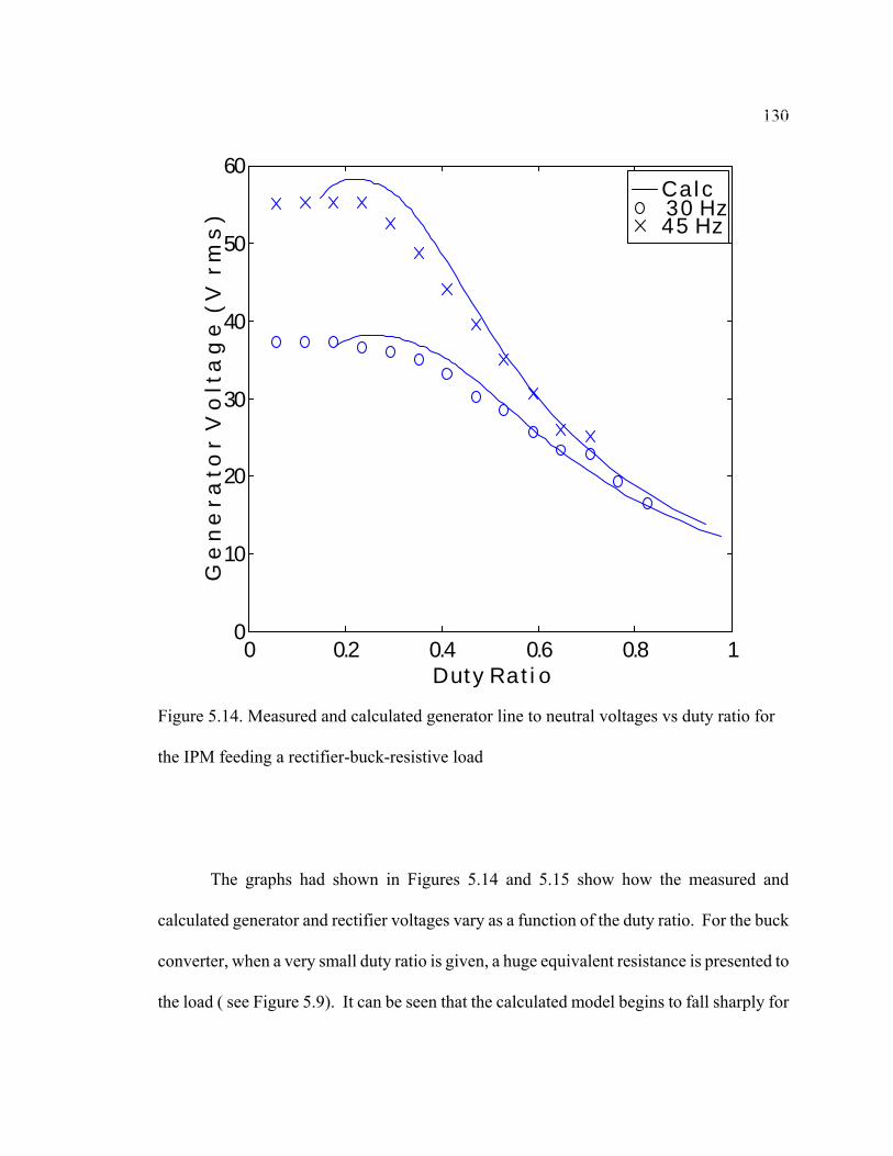
Figure 5.14. Measured and calculated generator line to neutral voltages vs duty ratio for
the IPM feeding a rectifier-buck-resistive load
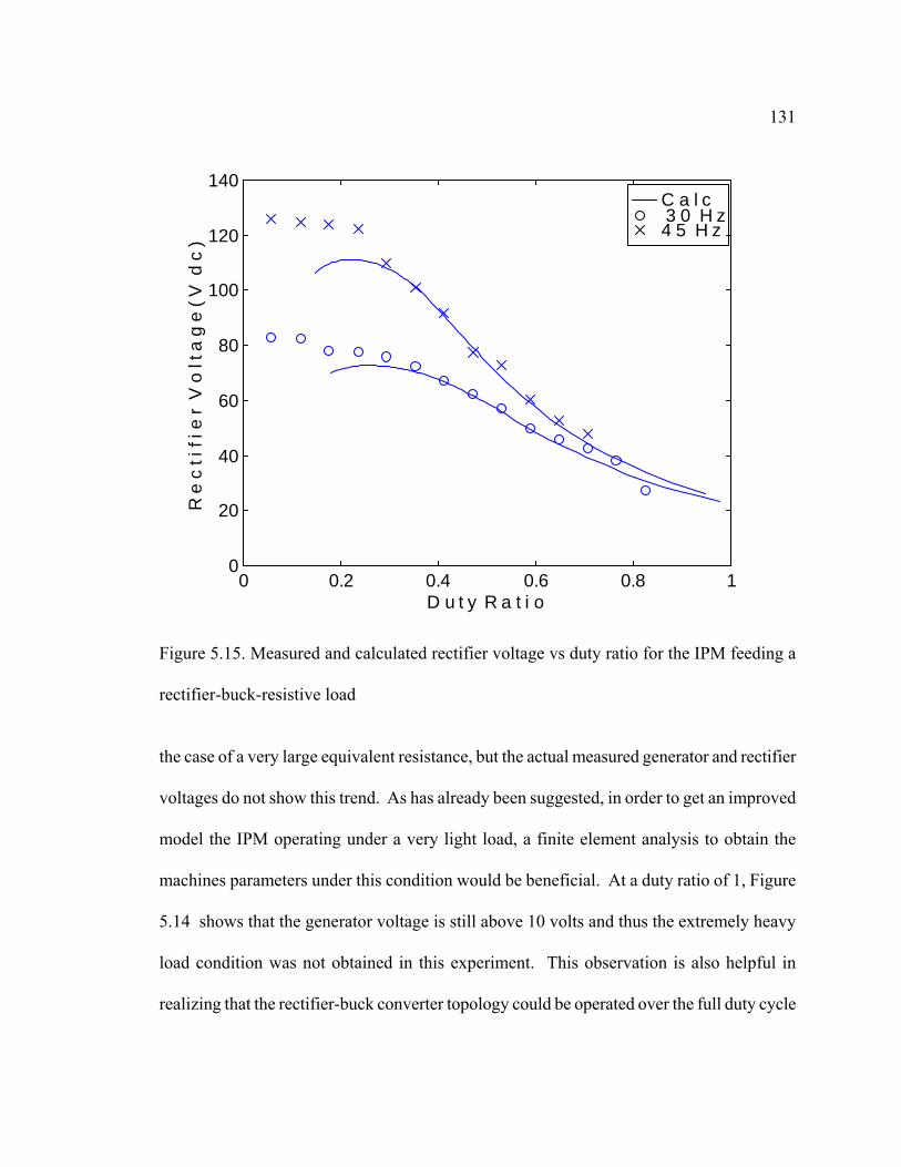
The graphs had shown in Figures 5.14 and 5.15 show how the measured and
calculated generator and rectifier voltages vary as a function of the duty ratio. For the buck
converter, when a very small duty ratio is given, a huge equivalent resistance is presented to
the load ( see Figure 5.9). It can be seen that the calculated model begins to fall sharply for
C a l c 3 0 H z 4 5 H z
0 0.2 0.4 0.6 0.8 10
10
20
30
40
50
60
D u t y R a t i o
G e
n e
r a
t o r
V o
l t a
g e
( V
r m
s )
131
C a l c 3 0 H z 4 5 H z
0 0.2 0.4 0.6 0.8 10
20
40
60
80
100
120
140
D u t y R a t i o
R e
c t
i f i
e r
V o
l t a
g e
( V
d c
)
Figure 5.15. Measured and calculated rectifier voltage vs duty ratio for the IPM feeding a
rectifier-buck-resistive load
the case of a very large equivalent resistance, but the actual measured generator and rectifier
voltages do not show this trend. As has already been suggested, in order to get an improved
model the IPM operating under a very light load, a finite element analysis to obtain the
machines parameters under this condition would be beneficial. At a duty ratio of 1, Figure
5.14 shows that the generator voltage is still above 10 volts and thus the extremely heavy
load condition was not obtained in this experiment. This observation is also helpful in
realizing that the rectifier-buck converter topology could be operated over the full duty cycle
132
C a l c 3 0 H z 4 5 H z
0 0.2 0.4 0.6 0.8 10
100
200
300
400
500
600
D u t y R a t i o
G e
n e
r a
t o r
P o
w e
r (
W )
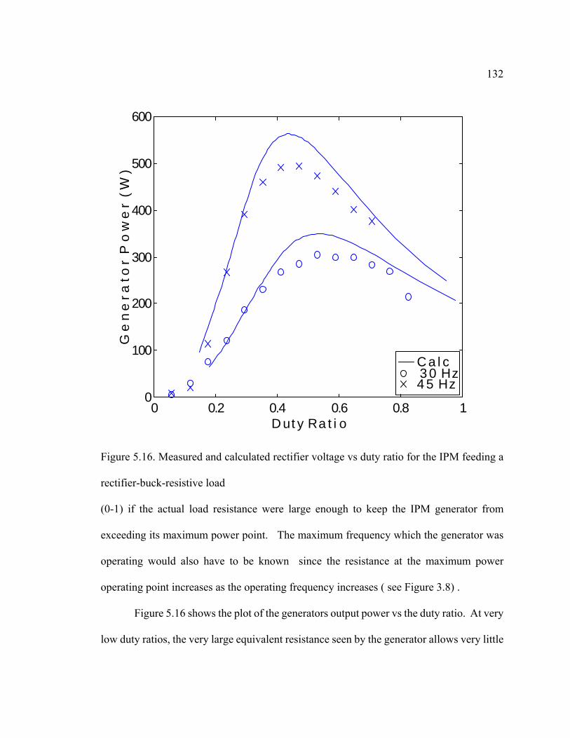
Figure 5.16. Measured and calculated rectifier voltage vs duty ratio for the IPM feeding a
rectifier-buck-resistive load
(0-1) if the actual load resistance were large enough to keep the IPM generator from
exceeding its maximum power point. The maximum frequency which the generator was
operating would also have to be known since the resistance at the maximum power
operating point increases as the operating frequency increases ( see Figure 3.8) .
Figure 5.16 shows the plot of the generators output power vs the duty ratio. At very
low duty ratios, the very large equivalent resistance seen by the generator allows very little
133
C a l c 3 0 H z 4 5 H z
0 0.2 0.4 0.6 0.8 10
1
2
3
4
5
6
7
D u t y R a t i o
G e
n e
r a
t o r
C u
r r e
n t
( A
r m
s )
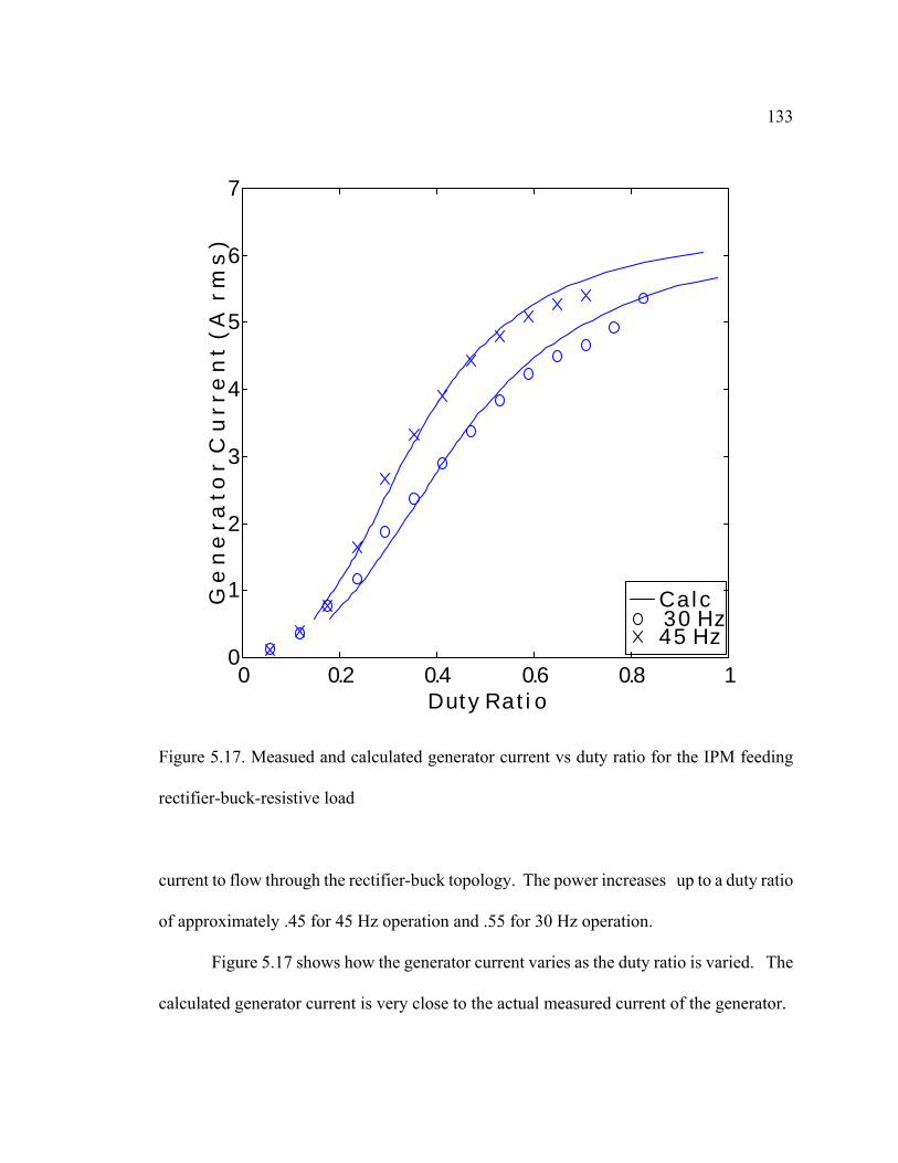
Figure 5.17. Measued and calculated generator current vs duty ratio for the IPM feeding
rectifier-buck-resistive load
current to flow through the rectifier-buck topology. The power increases up to a duty ratio
of approximately .45 for 45 Hz operation and .55 for 30 Hz operation.
Figure 5.17 shows how the generator current varies as the duty ratio is varied. The
calculated generator current is very close to the actual measured current of the generator.
134
C a l c 3 0 H z 4 5 H z
0 0.2 0.4 0.6 0.8 10
5
10
15
20
25
30
35
40
D u t y R a t i o
L o
a d
V o
l t a
g e
( V
d c
)
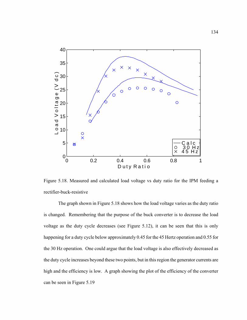
Figure 5.18. Measured and calculated load voltage vs duty ratio for the IPM feeding a
rectifier-buck-resistive
The graph shown in Figure 5.18 shows how the load voltage varies as the duty ratio
is changed. Remembering that the purpose of the buck converter is to decrease the load
voltage as the duty cycle decreases (see Figure 5.12), it can be seen that this is only
happening for a duty cycle below approximately 0.45 for the 45 Hertz operation and 0.55 for
the 30 Hz operation. One could argue that the load voltage is also effectively decreased as
the duty cycle increases beyond these two points, but in this region the generator currents are
high and the efficiency is low. A graph showing the plot of the efficiency of the converter
can be seen in Figure 5.19

135
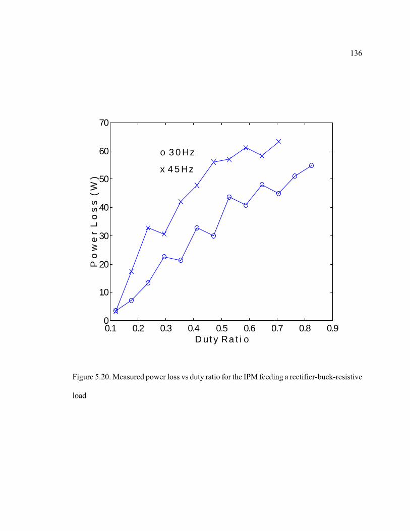
Figure 5.20 shows the plot of the measured power loss of the rectifier-buck system. It can
be seen that as the duty ratio increases, the power loss increases. This is true even beyond
the duty ratios when the power into the system has begun to decrease.
Figure 5.19. Plot of converter efficiency vs duty ratio for the IPM feeding a rectifier-buck
resistive load topology
0.1 0.2 0.3 0.4 0.5 0.6 0.7 0.8 0.90.75
0.8
0.85
0.9
0.95
1
C o
n v
e r
t e r
E f
f i c
i e
n c
y
o 3 0 H z
x 4 5 H z
136
Figure 5.20. Measured power loss vs duty ratio for the IPM feeding a rectifier-buck-resistive
load
0.1 0.2 0.3 0.4 0.5 0.6 0.7 0.8 0.90
10
20
30
40
50
60
70
D u t y R a t i o
P o
w e
r L
o s
s (
W )
o 3 0 H z
x 4 5 H z

137
5.4 Modeling of the Transistor
The modeling of a transistor in Simulink is similar to the model of the diode, except
that the time the switch is on and the time in which the switch is off is controlled externally,
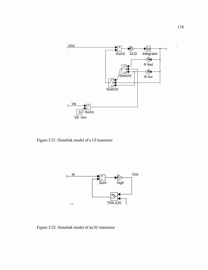
and is not dependent on the voltage across or the current through the device. Figure 5.21
shows the Simulink block diagram of a UI transistor. In order for the transistor switch to be
closed, the voltage across the transistor Vce must be positive, and the control signal Vb must
be above some threshold. For the example given in Figure 5.21, the threshold for Vb is .5
volts. Employing the same method of using a high gain to convert a UI diode into an IU
diode, Figure 5.22 shows the Simulink model of an IU transistor. The Simulink symbolic
representations of the UI and IU transistors are shown in Figures 5.23(a) and 5.23(b).
As has already been discussed in the introduction of this chapter, the method used
in this thesis to control the switching was to compare the waveforms of a triangle wave with
that of a dc signal. Figure 5.24(a) shows the triangle and dc waveforms superimposed on
one another. The magnitude of the dc signal divided by the peak value of the triangular
signal is referred to as the duty cycle (or duty ratio). For the example shown, the duty cycle
is 0.8. When the dc signal is larger than the triangle wave, a signal large enough to
overcome the bias voltage is sent to the transistor to turn it on. When the dc signal is smaller
than the triangle wave, the signal to the transistor is turned off and, thus, the transistor is
turned off. The resulting signal sent to the transistor is shown in Figure 5.24(b). Thus, the
amount of time which the transistor is on can be controlled by the magnitude of the dc
signal. For a duty cycle of 1, the transistor is always on.
138
Figure 5.21. Simulink model of a UI transistor
Figure 5.22. Simulink model of an IU transistor
Switch2
Switch1
-K-1/LD
I
+-
Sum1.5Vb min
1/sIntegrator
+-
Sum2
Vce
Vb
-KR rev
-KR fwd
Ie-K-high
+-
Sum
Vce
Vb TRA (UI)

139
Figure 5.23. Simulink symbolic representation of (a) a UI transistor and (b) an IU transistor
Figure 5.24. Generation of switching scheme for transistor. (a) a dc signal superimposed
upon a triangle wave, (b) signal sent to a transistor
0.025 0.03 0.0350
0.5
1
( a )
0
0.5
1

140
5.5 Comparison of Measured and Simulated Waveforms of IPM Machine Feeding a
Rectifier- Buck-Resistive Load
This section includes the comparison between simulation and measured waveforms
for the IPM generator feeding a rectifier-buck-resistive load. Two cases will be looked at.
The first is when the buck converter is operating in continuous conduction mode, and the
second is when the converter is operating in discontinuous conduction mode.
5.5.1 Buck Converter in Continuous Conduction Mode
This section looks at measured and simulated waveforms when the IPM is feeding a
rectifier-buck-resistive load topology for the case when the buck is operating in continuous
conduction mode. The frequency of operation of the IPM machine is 30 Hz. The rectifier
filter inductor and capacitor values are Ld =10mH and C1 = 5.6µF, the buck filter inductor
and capacitor values are Lp =10mH and Co=5.8µF, and the load resistance value is RL = 10Ω.
The duty cycle was set at .83.
Figures 5.25 and 5.26 show the simulated and measured line to line voltage and line
current waveforms of the IPM generator. The comparison between the simulated and
measured waveforms is favorable.

141
Measurement Simulation Figure 5.25. Measured and simulated line to line voltage waveforms for the generator feeding a rectifier-buck-resistive 10Ω resistive load. Rotor speed=900 rpm. Measured waveform scale: voltage: 50v/div, time 10ms/div
Figure 5.27 shows the measured and simulated current in the inductor Lp . It can be
seen from the figure that, similar to the current Ip depicted in Figure 5.5, the current rises
almost linearly when the transistor is turned on and falls linearly when the transistor is
turned off; however, unlike the current in Figure 5.5, measured and simulated currents never
Become equal to zero. In other words, since the current Ip always has a positive value, the
converter is operating in continuous conduction mode. Figure 5.28 shows the measured and
simulated current through the transistor T1.
0 0.02 0.04 0.06 0.08 0.1-200
-150
-100
-50
0
50
100
150
200
V a
b (
V )
T i m e ( s )

142
Measurement Simulation Figure 5.26. Measured and simulated generator current waveforms for the generator feeding a rectifier-buck-resistive 10Ω resistive load. Rotor speed=900 rpm. Measured waveform scale: current: 1A/div, time 5ms/div
Measurement Simulation
Figure 5.27. Measured and simulated buck inductor current waveforms for the generator feeding a rectifier-buck-resistive 10Ω resistive load. Rotor speed=900 rpm. Measured waveform scale: current: .1A/div, time .2ms/div
0.434 0.4345 0.435 0.4355 0.4363
3.2
3.4
3.6
3.8
4
4.2
T i m e ( s e c )
I n
d u
c t o
r C
u r
r e n
t (
A )
0 0.01 0.02 0.03 0.04 0.05-4
-3
-2
-1
0
1
2
3
4
I a g
( A
)
T i m e ( s )

143
Measurement Simulation Figure 5.28. Measured and simulated buck transistor current waveforms for the generator feeding a rectifier-buck-resistive 10Ω resistive load. Rotor speed=900 rpm. Measured waveform scale: current: 1A/div, time .2ms/div
5.5.2 Buck Converter in Discontinuous Conduction Mode
In this section, the inductor Lp is changed from the value of 10mH used in section
5.42 to the value of .25mH. In addition, the duty cycle is changed from .83 to a value of .2.
With these changes, the buck converter no longer operates in continuous conduction mode;
rather, it operates in discontinuous conduction mode.
0.434 0.4345 0.435 0.4355 0.436-2
-1
0
1
2
3
4
5
T i m e ( s e c )
T r
a n
s i s
t o
r C
u r
r e n
t (
A )
144
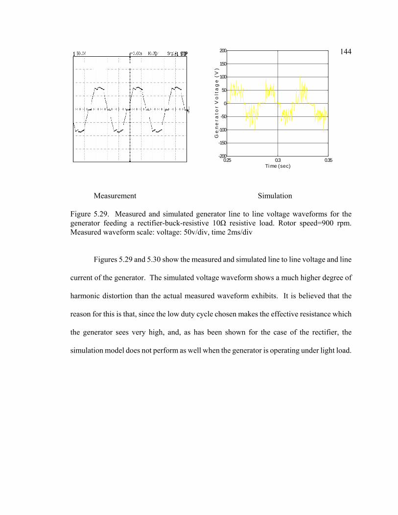
Measurement Simulation Figure 5.29. Measured and simulated generator line to line voltage waveforms for the generator feeding a rectifier-buck-resistive 10Ω resistive load. Rotor speed=900 rpm. Measured waveform scale: voltage: 50v/div, time 2ms/div
Figures 5.29 and 5.30 show the measured and simulated line to line voltage and line
current of the generator. The simulated voltage waveform shows a much higher degree of
harmonic distortion than the actual measured waveform exhibits. It is believed that the
reason for this is that, since the low duty cycle chosen makes the effective resistance which
the generator sees very high, and, as has been shown for the case of the rectifier, the
simulation model does not perform as well when the generator is operating under light load.
0.25 0.3 0.35-200
-150
-100
-50
0
50
100
150
200
T i m e ( s e c )
G e
n e
r a
t o r
V o
l t a
g e
( V
)

145
Measurement Simulation Figure 5.30. Measured and simulated generator line current waveforms for the generator feeding a rectifier-buck-resistive 10Ω resistive load. Rotor speed=900 rpm. Measured waveform scale: current: .5A/div, time 2ms/div
It can be seen in Figure 5.31 that the converter is clearly operating in discontinuous
conduction mode. It is also worthwhile to note the difference in the current in the measured
waveform of Figures 5.31 and 5.32 ( where the converter is in discontinuous mode) to the
measured inductor and transistor currents of Figures 5.27 and 5.28. When the converter is in
discontinuous mode it can be seen that both the peak current and the change in current from
its minimum to maximum value is much larger than when the converter is operating in
continuous conduction mode. The high stresses placed on the transistors due to the large
currents and large rate of change in currents (di/dt) is one of the main reasons why, for
practical designs, the discontinuous mode of operation is normally avoided.
0.25 0.3 0.35-2
-1.5
-1
-0.5
0
0.5
1
1.5
2
T i m e ( s e c )
G e
n e
r a
t o r
C u
r r e
n t

146
Measurement Simulation Figure 5.31. Measured and simulated inductor current waveforms for the generator feeding a rectifier-buck-resistive 10Ω resistive load. Rotor speed=900 rpm. Measured waveform scale: current: 5A/div, time .2ms/div
Measurement Simulation Figure 5.32. Measured and simulated transistor current waveforms for the generator feeding a rectifier-buck-resistive 10Ω resistive load. Rotor speed=900 rpm. Measured waveform scale: current: 2A/div, time .2ms/div
0.215 0.2155 0.216 0.2165 0.217-2
0
2
4
6
8
10
12
14
T i m e ( s e c )
T r
a n
s i s
t o
r C
u r
r e n
t (
A )
0.215 0.2155 0.216 0.2165 0.217-20
-15
-10
-5
0
5
10
15
20
T i m e ( s e c )
I n
d u
c t o
r C
u r
r e n
t (
A )