chapter 3 cmos low noise amplifiersshodhganga.inflibnet.ac.in/bitstream/10603/13446/8/08_chapter...
TRANSCRIPT

46
CHAPTER 3
CMOS LOW NOISE AMPLIFIERS
3.1 INTRODUCTION
The Low Noise Amplifier (LNA) plays an important role in the
receiver design. LNA serves as the first block in the RF receiver. It is a
critical building block since its performance greatly affects both sensitivity
and selectivity of the receiver. The main function of LNA is to amplify
extremely low signals without adding noise, preserving the required Signal-to
Noise Ratio (SNR) of the system at extremely low power levels.
Additionally, for large signal levels, the LNA should eliminate channel
interference. The purpose of LNA is to boost the signal power level for the
other circuits following the LNA in the receiver. Impedance matching is
important in LNA design as the system performance could be strongly
affected by the quality of the termination. For instance, the frequency
response of the antenna filter that precedes the LNA will deviate from its
normal operation if there are reflections from the LNA back to the antenna
filter.
LNA can be designed using lumped elements or distributed
elements. LNA design using lumped elements and distributed elements for
wideband applications are proposed by Challal et al (2008). Distributed LNA
operating in wide band from 0.5GHz to 5GHz proposed by Errikos
Lourandakis et al (2008) uses distributed elements. Distributed elements are
preferred wideband systems. For narrow band systems it is difficult to tune

47
the components. Hence LNA with active device and lumped elements are
considered for narrow band applications. In the wireless systems LNAs are
implemented using CMOS technology. CMOS LNAs with lumped elements
can be either single-ended or differential. Differential architecture requires the
use of a balun to transform the single-ended signal from the antenna into a
differential signal. Practical baluns introduce extra loss which adds directly to the
noise figure of the system, so single-ended architectures are preferred (Bosco
Leung 2002). Single-ended LNAs are preferred since most of the antenna
output is single-ended. Another reason for preferring single-ended LNA is
power consumption is less. In this chapter performance of single ended LNA
with lumped elements is studied.
In this chapter, narrow band single-ended Low Noise Amplifiers
(LNAs) using CMOS technology, operating in the 900MHz band and 2.4GHz
band are proposed and studied for beamforming in the receiver of wireless
systems. Two different LNAs, namely LNA1 working at center frequency of
902.5MHz with bandwidth of 25MHz from 890-915MHz and LNA2 working
at center frequency of 2.4 GHz with bandwidth of 20 MHz from 2390-
2410MHz are implemented using 0.35µm CMOS technology in ADS. Their
performance is compared with that of existing LNAs. It is found that the
proposed LNAs perform better in terms of various parameters.
3.2 LITERATURE SURVEY
While the literature is full of examples of LNA work in GaAs and
bipolar technology, there are few examples of CMOS studies. Table 3.1
shows literature study on LNAs operating in the range of 0.75GHz to 2.5GHz.
Their performance is compared based on the parameters like Noise figure
(NF), Gain, IIP3 (3rd
order Input Intercept Point) Power and Center frequency
of the amplifier.

48
Design of various LNAs is proposed by Shaeffer and Lee (1999). Resistive
termination LNA proposed by Chang et al (1993) using 2µm CMOS
technology provides a NF of 6dB. Two effects are responsible for the
degradation in noise figure. First, the added resistor contributes its own noise to
the output which equals the contribution of the source resistance. Second, the
input is attenuated by the resistor.
Table 3.1 Previous works on LNA
Author
Noise
Figure
(dB)
Gain
(dB)
IIP3
(dBm)
Power
(mW)
Frequency
(GHz)
Chang et al (1993) 6.0 14 -- 7 0.75
Sheng et al (1996) 7.5 11.0 -- 36 0.9
Andrew Karanicolas
(1996)2.2 15.5 12.4 20 0.9
Shaeffer and Lee
(1997)3.5 22 -9.5 30 1.5
Shahhani et al (1997) 3.8 17 -6 12 1.5
Johnson et al (1997) 2.8 10 4 14 2.4
Shunt-series feedback LNA proposed by Sheng et al (1996) using
0.8µm CMOS technology provides a NF of 7.5dB. Evgeniy Balashov and
Alexander Korotklov (2008) proposed LNA with source degeneration and
shunt series feedback for wideband systems. LNA using shunt-series feedback
often has high power dissipation compared to others with similar noise
performance. The higher power is partially due to the fact that such amplifiers
are naturally broadband and hence techniques which reduce the power
consumption through LC tuning are not applicable. LNA with shunt-series
feedback is not suitable for narrowband applications.
49
LNA with inductive source degeneration proposed by Shahhani
et al (1997) using 0.35µm CMOS technology provides good gain and low NF
but the stability of the amplifier is not discussed. Pietro Andreani and Henrik
Sjoland (2001) has proposed LNA with cascode transistor and noise
optimization. Only noise is minimized and gain, bandwidth and other
parameters are not discussed. There is still a requirement for stable LNAs
with high gain, low power consumption, low noise figure and good linearity.
In this thesis, an attempt is made to propose LNAs with high gain, low NF,
stability and good linearity.
3.3 CMOS NARROW BAND LNA
CMOS Narrowband LNAs has the advantages like low power
consumption and low-noise performance (Challal et al 2008). The primary
design challenge in LNA design is to maximize gain without adding excessive
noise into the signal. As LNA is next immediate to antenna, proper impedance
matching is required between these two devices to avoid the reflection of
power back to antenna. The input and output impedance of the LNA is 50 as
specified in specifications of wireless systems. Since the input impedance of
the MOS transistor is almost purely capacitive, providing a good match to the
source without degrading noise performance is a challenge. There is a subtle
difference between impedance matching and power matching. The condition
for impedance matching occurs when the load impedance is equal to the
characteristic impedance. However, the condition for power matching occurs
when the load impedance is the complex conjugate of the characteristic
impedance. When the impedances are real, the conditions for power matching
and impedance matching are the same. An impedance is matched when
ZS = ZL as shown in Figure 3.1.
The LNAs proposed are compared with existing LNAs based on
number of parameters like voltage gain, Noise Figure (NF), SNR, S-

50
parameters, stability, Spurious Free Dynamic Range (SFDR), 1-dB
compression point, 3-dB compression point and Third order Intercept Point
(IP3). Voltage gain gives the amount by which the signal at input of the LNA
is amplified. Noise Figure (NF) specifies the additive noise inherent in the
LNA circuit. NF is used to describe the degradation of Signal to Noise Ratio
(SNR) by the active device in the LNA. NF is defined as the ratio of SNR at
input of the LNA to SNR at the output of the LNA. NF must be very low at
the center frequency for the designed LNA. SNR can be found at the input
and output of any amplifier circuit. The SNR at the output of LNA must be
very high. SFDR is defined by Joel Lawrence Dawson and Thomas Lee
(2004) as the SNR when the power in each 3rd order intermodulation product
equals noise power at the output. High value of SFDR is preferred for the
LNA circuit to be free from spurious signals.
VS
ZS=RS+jXS
ZL=RL+jXL=ZS
Figure 3.1 Conditions for Impedance Match
The stability of the LNA is found using stability factors like Rollet
stability factor and Edwards-Sinsky stability parameter (Pozar 2005). The
Rollet stability factor (K) in terms of S-parameters is given by (3.1) as

51
2 2 2
11 22
11 21
1 S SK
2 S S (3.1)
where is given as
11 22 12 21(S S ) (S S ) (3.2)
If K > 1 and < 1, then the circuit will be unconditionally stable
for any combination of source and load impedances. For K < 1 the device is
potentially unstable and will most likely oscillate with certain combinations of
source and load impedance. The Edwards-Sinsky stability parameter (µ1) is
given by (3.3) as
2
11
1
22 11 12 21
1 S1
S S S S (3.3)
If µ1 >1 and <1, the circuit is unconditionally stable. Based on the
S-parameters various gains like Power Gain (PG), Transducer Power Gain
(TPG) and Available Power Gain (APG) are found for the LNA. Power Gain
is defined as the ratio of the power delivered to the load and the average
power delivered to the circuit from the input and is given by (3.4) as
2
21
2
11
SPG
1 S (3.4)
The Power Gain is same as the voltage gain in LNA when the
circuit is perfectly impedance matched. Transducer Power Gain (TPG) is
defined as the ratio of the output power delivered to a load by a source and the
maximum power available from the source and is given in (3.5). It includes
the effects of input and output impedance matching. Component resistive
losses are neglected.

52
2 2 2
21 S L
2
11 S 22 L 12 21 L S
S (1 ) (1 )TPG
[(1 S )(1 S )] S S (3.5)
The Available Power Gain (APG) is the ratio of the power available
from the output port of the network to the power available from the source
and is given as
2
21
2
22
SAPG
1 S (3.6)
1 dB compression point of an LNA is the input voltage level at
which the gain of the LNA drops by 1dB. 1dB compression point is a measure
of gain compression which indicates the nonlinearity of LNA. When the input
signal given to the amplifier has large amplitude, the amplifier saturates and
there is clipping of the signal at output. When the strength of the input is
further increased, the output signal is no longer amplified and at this point the
output is compressed.
3dB compression point is also of importance in studying the
performance of LNA. An LNA, like any active component in the receiver, has
a dynamic range. If a signal of sufficient amplitude is presented to its input,
the LNA output will compress and the gain of the LNA will reduce. The 3dB
compression point is the input signal amplitude at which the LNA gain is
reduced by 3dB. When the LNA goes into compression, there is less gain
available to amplify the wanted signals, thereby reducing the receiver’s
sensitivity. In the wireless receivers, this phenomenon occurs when the
receiver is close to a cellular phone tower. There are two ways to improve the
performance of the receiver. One is to select a receiver with LNA having the
highest 3dB compression point and second method is to place a filter in front
of the LNA that attenuates out-of-band signals.

53
IP3, the third order inter-modulation product rejection, is a measure
of how well a receiver handles inter-modulation. Basically, inter-modulation
occurs when two or more strong signals (also called tones) are being received
from transmitters transmitting on frequencies other than the receiver’s current
frequency. When the two tones hit the down-conversion mixer, they produce
additional frequencies that are the sum and difference. The sum product is
usually of no concern because it is well outside the receiver’s pass band. The
difference product, however, is important because it could easily fall inside
the receiver’s pass band. So, rejecting these product frequencies (also called
inter-modulation) is important. Therefore, the higher the IP3 number, the
better. The specifications for the design of LNA operating at 900MHz band
and 2.4GHz band are given in the Table 3.2.
Table 3.2 Specifications for design of LNAs
Parameter Specification
Frequency band 900MHz 2.4GHz
Center frequency 902.5MHz 2.4GHz
Bandwidth 25MHz 20MHz
Stability factor K and K>1 and <1
Noise figure <6dB
Gain >10dB
Power consumption <100mW
SFDR >30dB
SNR >70dB
3.4 CMOS SINGLE ENDED LNAs
Commonly existing narrowband single ended LNA architectures
with lumped elements are Resistive termination, shunt-series feedback and

54
inductive source degeneration. An NMOS transistor added in cascode to the
existing amplifier improves the performance of the LNAs as proposed by
Hajiz Fouad et al (2002). The performance of LNA with resistive termination,
shunt-series feedback and inductive source degeneration are compared with
existing LNAs.
3.4.1 LNA with Resistive Termination
LNA uses resistive termination of the input port to provide 50
impedance to suppress reflection at the input. Also the input impedance of the
LNA must match the output impedance of the preceding stage. Resistive
termination is the most straightforward approach to achieve the broadband
50 matching at the input of LNA as shown in Figure 3.2.
Vout
MOSFET 1
-
+VDD=3.3V
Vin R1
R2
L
MOSFET 2
Figure 3.2 Circuit of Resistive termination matched LNA
The 50 -resistor (R1) is placed across the input terminal of the
LNA and hence providing a broadband input matching. The bandwidth of this
amplifier is determined by the input capacitance of the transistor MOSFET 1

55
and is normally very high. MOSFET 2 is the transistor added in cascode to
improve the performance. However, the resistor R1 adds its own thermal
noise to the circuit as well as attenuates the incoming signal before it hits the
gate of the transistor. These two effects result in an unacceptably high NF of
the circuit and less tuning capability of the amplifier bandwidth and hence not
practically used in most applications.
3.4.2 LNA with Shunt-Series Feedback
The second method used for getting a good input matching is the
shunt-series feedback amplifier which uses resistive shunt-series feedback to
set the input and output impedances of the LNA as shown in Figure 3.3.
Vin
Vout
MOSFET 1
MOSFET 2
R1
C4
-
+
R4
C3
L2
VDD=3.3V
L1
Figure 3.3 Circuit of Shunt-series feedback matched LNA
Unlike in the resistive termination case, this circuit does not
attenuate the signal by a noisy attenuator before reaching the gate of the
amplifying device and hence the Noise Figure is expected to be much better.

56
The advantage of having inductance L1 at the gate of the NMOS is that this
inductance cancels out the gate to source capacitance of the NMOS at the
resonant frequency and hence making the impedance at the input of the
NMOS to be real i.e., only input resistance (Rin). However, the feedback
resistor continues to generate thermal noise of its own. This results in the
relatively high Noise Figure, usually a few decibels above the given
specification. The shunt-series architecture requires on-chip resistors of
reasonable quality, which are generally not available in CMOS technology.
3.4.3 LNA with Inductive Source Degeneration
The inductive source degeneration provides a perfect match without
adding any noise to the system or giving any restrictions on the device
transconductance (gm). It uses an inductor as a source degeneration device and
has another inductor connecting to the gate. This architecture employs
inductive source degeneration to generate a real term in the input impedance.
Tuning of the amplifier input becomes necessary, making this a narrow-band
amplifier. Inductive source degeneration is the most prevalent method used
for many amplifiers. It offers the possibility of achieving the best noise
performance of any architecture. The LNA with inductive source
degeneration performs better than resistive termination LNA and shunt-series
feedback LNA.
The performance of LNA with inductive source degeneration is
improved by proposing LNA with diode connected NMOS transistor at the
input acting as resistance and an additional NMOS transistor in cascode
configuration at the load of the LNA. Diode connected transistor at input
provides better gain and tuning of bandwidth. LNA1 is LNA operating at
center frequency of 902.5MHz and LNA2 is LNA operating center frequency
of 2.4GHz. The performance of LNA1 and LNA2 is compared with that of
existing narrow band LNA architectures.

57
3.4.3.1 Proposed Single ended LNA without Cascode transistor
LNA with inductive source degeneration and diode connected
transistor is proposed. LNA without diode connected transistor is proposed by
Shahhani et al (1997) and Johnson et al (1997). These LNAs provides high
gain but large bandwidth and are wide band amplifiers. To make the amplifier
as narrow band diode connected transistor is used at the input for biasing and
tuning of bandwidth. The circuit of proposed LNA without cascade transistor
is shown in Figure 3.4.
Vin
Vout
MOSFET 1
R1 C1
-
+
R3
R2
L2
MOSFET 2
VDD=3.3V
L1
L3
Figure 3.4 Proposed Single ended LNA circuit without Cascode transistor
Diode connected transistor, MOSFET2 used at the input acts as
resistance to improve the impedance matching at the input of the LNA. The
advantage of using inductor L1 is that biasing is done without significant dc
voltage drop. L1 acts as source degeneration for MOSFET1 which increases
the linearity without noise penalty. Maximization of the quality factor (Q) of
the inductor allows low losses in the circuit and superior performance when
used in matching networks, oscillators and biasing networks. High Q results
in low phase noise, low noise figure of the LNA, low loss matching networks,

58
lower power consumption and improved receiver sensitivity. Proposed LNAs
are designed with inductor having high Q.
3.4.3.2 Proposed Single ended LNA with Cascode transistor
In the proposed LNA, transistor is used in cascode configuration at
the load. The advantage of cascode configuration is given by Hajiz Fouad et
al (2002). Cascode is a combination of a common-source device with a
common-gate load. This has the effect of increasing the output impedance. If
a resistive load is used and if LNA is to be connected to another stage i.e.,
another LNA or mixer, then the load will be capacitive. This capacitance will
limit the frequency response of the first amplifier stage and results in lower
gain due to the Miller effect. Proposed Single ended LNA circuit with
Cascode transistor is shown in Figure 3.5.
Vin
Vout
MOSFET 1
R1 C1
- +
R3
R2
L2
MOSFET 2
VDD=3.3V
L1
MOSFET 3
L3
Figure 3.5 Proposed Single ended LNA circuit with Cascode transistor
The inductor, L3 between the cascode source and supply in the
Figure 3.5 blocks any RF leaking to the supply rail and may be varied in value
to optimize the gain response of the LNA. The additional cascode device has
been configured as a diode (i.e., at DC the gate is connected to the source) as
shown in Figure 3.5.
59
3.5 PARAMETERS OF MOSFET FOR PROPOSED SINGLE
ENDED LNAs
The design of LNA given in Shaeffer et al (1999) is used in this
thesis. The NMOS Transistor with 0.35µm CMOS technology chosen for
design of LNAs has the following parameters: oxide thickness (Tox), 7.7 nm;
Threshold Voltage (Vt), 0.508216V; minimum length (Lmin), 0.4µm;
minimum width (Wmin), 0.90µm; mobility of electrons (µn), 153.89 cm2/V-s;
permittivity of silicon ( Si), 11.7 o and permittivity of the substrate ( ox),
3.97 o, where o=8.85e-12
F/m.
The equations for finding various parameters of the LNA without
cascode transistor are given as follows:
The cut-off frequency of MOSFET is given by (3.7) as
mO
gs
g
C (3.7)
O is the angular cut-off frequency, mg is the transconductance of
the MOSFET and Cgs is the gate to source capacitance of the MOSFET.
Optimal Q of the inductor is given by
1Q 1
p (3.8)
where
2
p5
(3.9)
The parameters of p are dependent on the CMOS technology used
and are specified in the model file of the transistors (www.mosis.org). The

60
parameters are typically set as =2; =4 and =0.9 from the model file. The
value of p is calculated from (3.9) as 0.162. The inductance (L2) at the gate of
the NMOS is given by the equation
L in
o
Q RL2 L1 (3.10)
where QL is the Q of the inductor, Rin is the input resistance at the gate of
NMOS, o is the angular center frequency given by o=2 fo. fo is the center
frequency in Hz. The gate to source capacitance (Cgs) of the NMOS is given
by the equation
gs 2
o
1C
(L2 L1) (3.11)
The width of NMOS is given as
g s
o x m in
C3W
2 C L (3.12)
where Cox is the oxide capacitance given by Cox= ox /Tox. The
transconductance (gm) of the NMOS is given as
m O g sg C (3.13)
and the total voltage to be applied at the gate of the NMOS is VGS which is
sum of effective voltage (Veff) and threshold voltage (Vt) of NMOS. The
effective voltage at gate of NMOS is calculated as
me ff
n o x
gV
C W (3.14)
The bias current needed at the drain of NMOS is given by (3.15) as
61
D m eff
1I g V
2 (3.15)
The design procedure of LNA with cascode transistor is same as for
LNA without cascode transistor. The W/L ratio of MOSFET3 is same as that
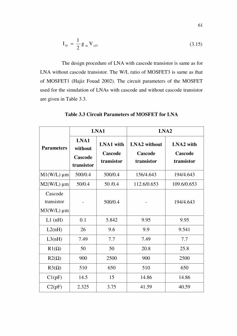
of MOSFET1 (Hajiz Fouad 2002). The circuit parameters of the MOSFET
used for the simulation of LNAs with cascode and without cascode transistor
are given in Table 3.3.
Table 3.3 Circuit Parameters of MOSFET for LNA
LNA1 LNA2
Parameters
LNA1
without
Cascode
transistor
LNA1 with
Cascode
transistor
LNA2 without
Cascode
transistor
LNA2 with
Cascode
transistor
M1(W/L) µm 500/0.4 500/0.4 156/4.643 194/4.643
M2(W/L) µm 50/0.4 50 /0.4 112.6/0.653 109.6/0.653
Cascode
transistor
M3(W/L) µm
- 500/0.4 - 194/4.643
L1 (nH) 0.1 5.842 9.95 9.95
L2(nH) 26 9.6 9.9 9.541
L3(nH) 7.49 7.7 7.49 7.7
R1( ) 50 50 20.8 25.8
R2( ) 900 2500 900 2500
R3( ) 510 650 510 650
C1(pF) 14.5 15 14.86 14.86
C2(pF) 2.325 3.75 41.59 40.59
62
3.6 SIMULATION RESULTS
Various simulations like AC simulation, S-parameter simulation
and Harmonic Balance simulation are performed to study the performance of
LNAs. The performance of the LNAs is verified using parameters like Gain,
Bandwidth, NF, SNR, SFDR, VSWR, 1-dB compression, stability, power
gain and IP3. The maximum frequency that the 0.35µm CMOS technology
can support is given in terms of unity-gain frequency (fT) (Hassan Hassan et
al 2006). Unity-gain frequency of N-channel MOSFET (NMOS) used for the
design of LNA using 0.35µm CMOS technology is the frequency at which the
current gain of the MOSFET is unity.
The unity-gain frequency for this NMOS is found using AC
simulation. In the AC simulation the operating point of NMOS device is
selected as 2.5V for both VGS and VDS, saturated with a significant
overdrive voltage in order to minimize the non-quasi static (NQS) effects.
Input current of 1mA is given at the gate of the NMOS transistor which is
biased with dc voltage of 2.5V. The voltage at the drain is 3.3V. AC
simulation is performed to find the variation of current gain with respect to
frequency. The fT obtained from AC simulation is shown in Figure 3.6 for
LNA1 and in Figure 3.7 for LNA2.
For the LNA1 the unity gain frequency is 19GHz. If this NMOS is
used for implementing LNA at center frequency of 902.5MHz there will not
be any NQS effects as there will not be any phase deviation till 20% of
19GHz i.e., 3.8GHz and no amplitude variations till fT. Hence this NMOS can
be used to implement LNAs at center frequency of 902.5MHz.

63
Figure 3.6 fT of MOSFET for LNA1
Figure 3.7 fT of MOSFET for LNA2
The unity gain frequency of LNA2 is 16GHz. If this NMOS is
used for implementing LNA at center frequency of 2.4GHz there will not be
any NQS effects as there will not be any phase deviation till 20% of 16GHz
i.e., 4GHz and no amplitude variations till fT. The drain current measured for
the NMOS is 22mA at 902.5MHz and is 7mA at 2.4GHz. The operating point

64
(VDS, ID) for NMOS device at 902.5MHz and 2.4GHz are (2.5V, 22mA) and
(2.5V, 7mA) respectively.
The AC simulation is performed to find the voltage gain, center
frequency of operation, bandwidth, NF and SNR of the LNA. The S-
parameter simulation is performed to find the S-parameters, stability, Power
gain, Available Power Gain (APG), Transducer Power Gain (TPG) and
Voltage Standing Wave Ratio (VSWR). Harmonic balance simulation is
performed to find the parameters like IP3, total power consumption, SFDR, 1-
dB compression point and 3-dB compression point of the LNA.
3.6.1 LNA with Resistive Termination and LNA with Shunt Series
Feedback
Performance of LNA with resistive termination and shunt series
feed back are found using simulation.
Table3.4 Simulation results of LNA
Parameters
LNA with
Resistive
Termination
LNA with
Shunt-Series
Feedback
Gain (dB) 28.535 29.031
S11 (dB) -1.735 -7.729
S12(dB) -29.769 -28.731
S21(dB) 7.998 8.181
S22(dB) -9.884 -7.222
NF(dB) 4.482 3.781
3dB input power (dBm) 20.61 5.382
3 dB output power (dBm) 26.52 10.42
1 dB input power (dBm) 16.03 -2.009
1 dB output power (dBm) 23.94 5.034

65
From the various parameters of resistive LNA and shunt series
feedback LNA given in Table 3.4, it is inferred that the gain is very low and
the NF is high. Another drawback in the above two circuits is, tuning of the
circuits for the required bandwidth is not easy as the components in the circuit
are mostly resistors. Hence LNA with inductive source degeneration is
implemented to provide better results.
3.6.2 Single Ended LNA1
The LNA1 without cascode transistor provides a maximum gain of
35.277dB at the designed center frequency of 902.5MHz and 3-dB bandwidth
of 36.5MHz against the requirement of 25MHz as shown in Figure 3.8 (a).
(a) Gain without Cascode transistor
(b) Gain with Cascode Transistor
Figure 3.8 Gain of LNA1
66
The LNA1 with cascode transistor at the output provides a
maximum gain of 44.806dB at the designed center frequency of 902.5MHz
and bandwidth of 61MHz as shown in Figure 3.8 (b).
The gain and bandwidth of the LNA1 with cascode transistor has
increased when compared with LNA1 without cascode transistor. Noise
Figure of LNA with cascode and without cascode transistor is shown in
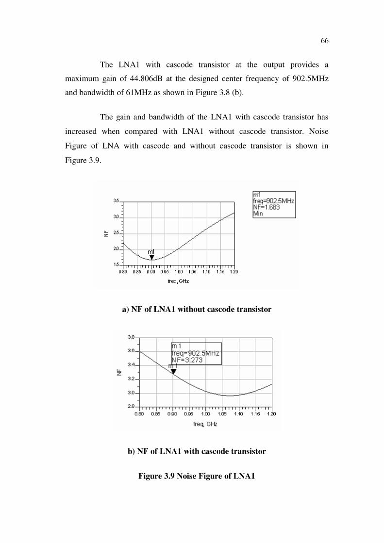
Figure 3.9.
a) NF of LNA1 without cascode transistor
b) NF of LNA1 with cascode transistor
Figure 3.9 Noise Figure of LNA1
67
The LNA1 without cascode and with cascode transistor provide a
very low NF of 1.683dB and 3.273dB respectively. The NF of LNA1 with
cascode transistor has increased which shows that noise has been added in the
circuit due to the addition of transistor in cascode, but still the NF satisfies the
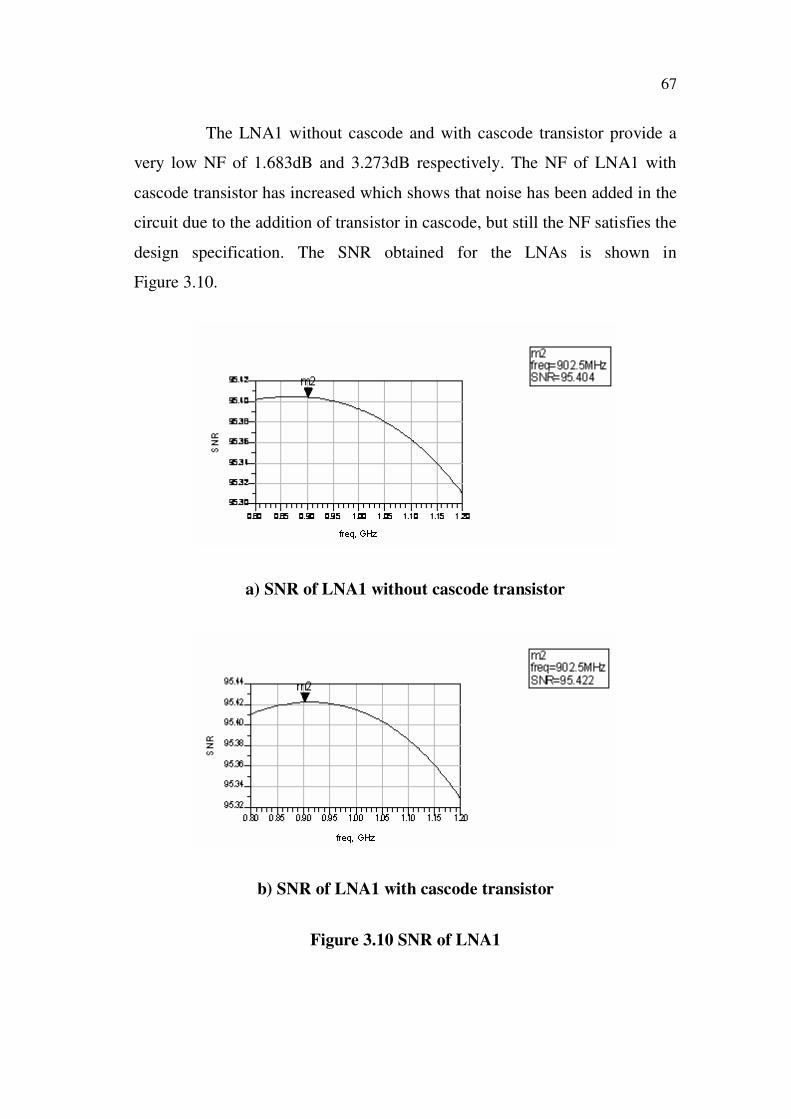
design specification. The SNR obtained for the LNAs is shown in
Figure 3.10.
a) SNR of LNA1 without cascode transistor
b) SNR of LNA1 with cascode transistor
Figure 3.10 SNR of LNA1

68
The LNA1 without cascode transistor gives a SNR of 95.404dB
and with cascode gives a SNR of 95.422dB. There is no significant difference
in SNR of both the LNAs. From the S-parameter simulation performed for the
LNA1 the various S-parameters obtained are given in Table 3.5. Harmonic
balance simulation is performed to find the parameters related to linearity of
the amplifier and the dynamic range of the LNA. The results of Harmonic
balance simulation are given in Table 3.6.
Table 3.5 S-parameter simulation results of LNA1
S-parameters LNA1 without
cascode transistor
LNA1 with
cascode transistor
S21 (dB) 9.966 11.689
S11 (dB) -5.244 -2.464
S12 (dB) -21.248 -51.756
S22 (dB) -8.110 -0.856
Rollett stability factor K 1.364 4.544
Stability measure 0.947 0.268
Edwards-Sinsky stability
parameter µ1
1.450 1.095
VSWR 3.412 7.098
Power gain (dB) 9.966 11.689
APG (dB) 14.154 34.073
TPG (dB) 9.923 14.752
69
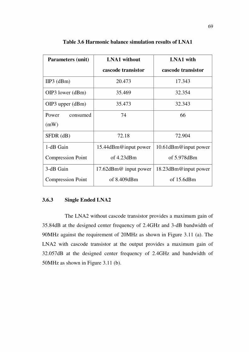
Table 3.6 Harmonic balance simulation results of LNA1
Parameters (unit) LNA1 without
cascode transistor
LNA1 with
cascode transistor
IIP3 (dBm) 20.473 17.343
OIP3 lower (dBm) 35.469 32.354
OIP3 upper (dBm) 35.473 32.343
Power consumed
(mW)
74 66
SFDR (dB) 72.18 72.904
1-dB Gain
Compression Point
15.44dBm@input power
of 4.23dBm
10.61dBm@input power
of 5.978dBm
3-dB Gain
Compression Point
17.62dBm@ input power
of 8.409dBm
18.23dBm@input power
of 15.6dBm
3.6.3 Single Ended LNA2
The LNA2 without cascode transistor provides a maximum gain of
35.84dB at the designed center frequency of 2.4GHz and 3-dB bandwidth of
90MHz against the requirement of 20MHz as shown in Figure 3.11 (a). The
LNA2 with cascode transistor at the output provides a maximum gain of
32.057dB at the designed center frequency of 2.4GHz and bandwidth of
50MHz as shown in Figure 3.11 (b).

70
(a) Gain without Cacode transistor
(b) Gain with Cascode transistor
Figure 3.11 Gain of LNA2
The gain and bandwidth of the LNA2 without cascode transistor is
high when compared with LNA2 with cascode transistor. The LNA2 without
cascode and with cascode transistors provide a very low NF of 1.15dB and
1.591dB respectively as shown in Figure 3.12.

71
a) NF of LNA2 without cascode transistor
b) NF of LNA2 with cascode transistor
Figure 3.12 Noise Figure of LNA2
The Noise Figure of LNA2 with cascode transistor has increased
which shows that noise has been added in the circuit due to the addition of
transistor in cascode, but still the Noise Figure satisfies the design
specification.
72
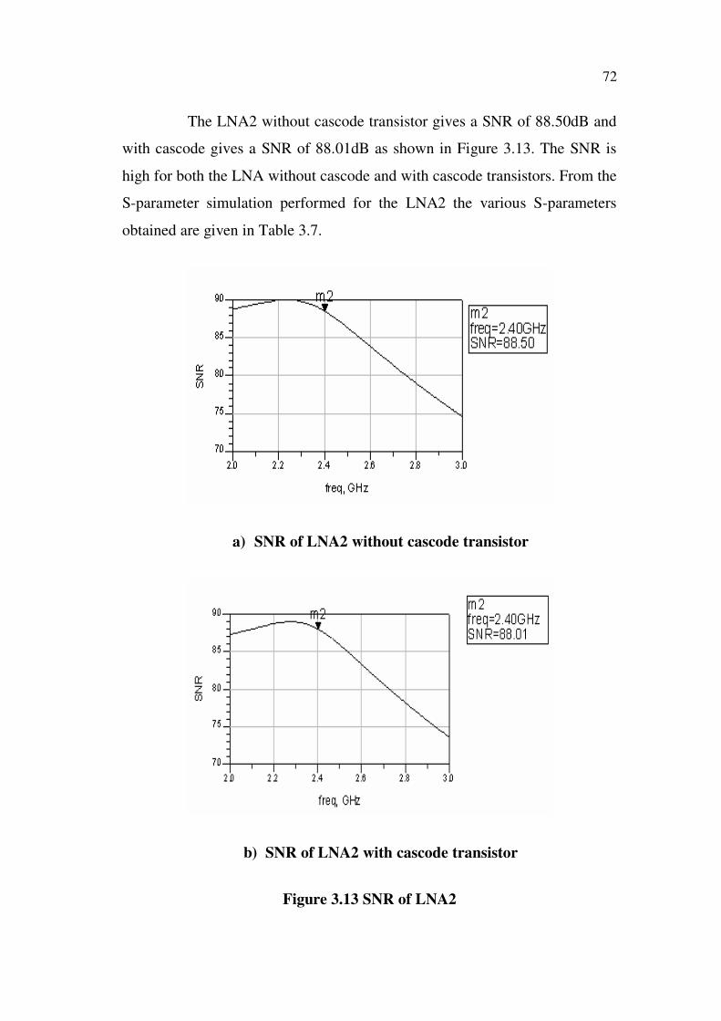
The LNA2 without cascode transistor gives a SNR of 88.50dB and
with cascode gives a SNR of 88.01dB as shown in Figure 3.13. The SNR is
high for both the LNA without cascode and with cascode transistors. From the
S-parameter simulation performed for the LNA2 the various S-parameters
obtained are given in Table 3.7.
a) SNR of LNA2 without cascode transistor
b) SNR of LNA2 with cascode transistor
Figure 3.13 SNR of LNA2

73
Table 3.7 S-parameter simulation results of LNA2
S-parameters LNA2 without
cascode transistor
LNA2 with
cascode transistor
S21 (dB) 16.728 11.101
S11 (dB) -7.286 -6.51
S12 (dB) -17.211 -22.622
S22 (dB) 0.933 -2.325
Rollett stability factor, K 1.186 22.666
Stability measure, 0.109 0.640
Edwards-Sinsky stability
parameter, µ1
1.018 1.495
VSWR 2.522 2.641
Power gain (dB) 16.728 11.101
APG (dB) 57.892 16.589
TPG (dB) 47.078 12.884
Harmonic balance simulation is performed to find the parameters
related to linearity of the amplifier and the dynamic range of the LNA. The
results of Harmonic balance simulation are given in Table 3.8.
Table 3.8 Harmonic balance simulation results of LNA2
Parameters
(unit)
LNA2 without
cascode transistor
LNA2 with
cascode transistor
IIP3 (dBm) 34.829 36.366
OIP3 lower (dBm) 19.774 21.462
OIP3 upper (dBm) 19.829 21.366
Power consumed (mW) 2 2
SFDR (dB) 36.511 33.099
1-dB Gain
Compression Point
24.04dBm@input power
of 16.93dBm
12.86dBm@input
power
of 3.122dBm
3-dB Gain
Compression Point
11.90@ input power
of 2.781dBm
11.98dBm@input
power
of 0.24dBm

74
The performance of proposed LNAs is compared with existing
architectures namely resistive termination and Shunt-Series feedback. The
proposed LNA with inductive source degeneration performs better. In the
proposed LNAs, LNA with cascode transistor at performs better than the
LNA without cascode transistor at 900MHz band and LNA without cascode
transistor at performs better than the LNA with cascode transistor in 2.4GHz
band.
3.7 CONCLUSION
LNA circuits are designed and analyzed for 900MHz and 2.4GHz
wireless systems. The results obtained from S-Parameter simulation, AC
simulation, DC simulation, and Harmonic balance simulation for IIP3, XDB
simulation for 3-dB gain compression and 1-dB gain compression show that,
the circuits are suitable for GSM900 systems and wireless systems operating
at 2.4GHz. In the 900MHz frequency band the LNA with resistive
termination provides a voltage gain of 28.535dB and minimum noise figure of
4.482. LNA with Shunt-series feedback provides a gain of 29.031dB and a
noise figure of 3.781. LNA1 with Inductive source degeneration provides a
gain of 35.277dB without cascode transistor. LNA1 with Inductive source
degeneration provides a gain of 44.806dB with cascode transistor. The NF of
LNA1 is lower than the noise figure of LNA with resistive termination and
shunt-series feedback. The LNA1 with inductive source degeneration
provides better results compared to resistive termination and shunt series
feedback LNAs. LNA1 provides better results than the similar LNAs
available in the literature.
LNA2 operating in the 2.4GHz frequency band provides high gain
and low noise figure when compared to the similar LNAs in the literature.
LNA2 also provides high SNR, SFDR and good linearity. The LNA1 and
LNA2 proposed are highly stable.