successes in rf cmos circuit design - es.lth.se · some successes 1st success: transmitter...
TRANSCRIPT

Successes in RF CMOS Circuit Design
Henrik Sjöland
2007-09-06
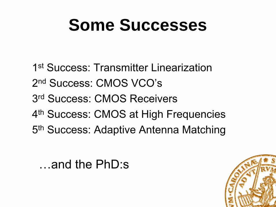
Some Successes
1st Success: Transmitter Linearization2nd Success: CMOS VCO’s3rd Success: CMOS Receivers4th Success: CMOS at High Frequencies5th Success: Adaptive Antenna Matching
…and the PhD:s

1st Success: Transmitter Linearization
• Major project in first 2 stages• Led by Dr. Lars Sundström• Important then – Even more important now!• Required for spectrally efficient systems (3G,LTE, ..)• Both in terminals and base stations• Analog & Digital Pre-Distortion• Power Feedback• LINC

Power Amplifier Characteristics

Principle ofPredistortion
PA
PAPD

Analog Predistortion
• 5th order complex polynomial• 3.3V, 20mA (only 30% in polynomial)• Bandwidth (3dB) 120MHz• Differential 200Ω interface• Hand-tuning of coefficients• Standard 0.8um CMOS process• ISCAS ’99• Improved circuit at ESSCIRC ’01
Eric Westesson

Saturated Class A PA without and with Predistortion
35dB
Eric Westesson
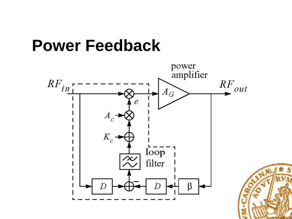
Power Feedback

Power FeedbackBo Shi
• 3.3V, 19mA• RF input bandwidth ~1GHz• Differential 200Ω interface• Standard 0.6um CMOS process• Presented at ISCAS ’99

Power Feedback –Spectrum and Efficiency
10dB
Bo Shi
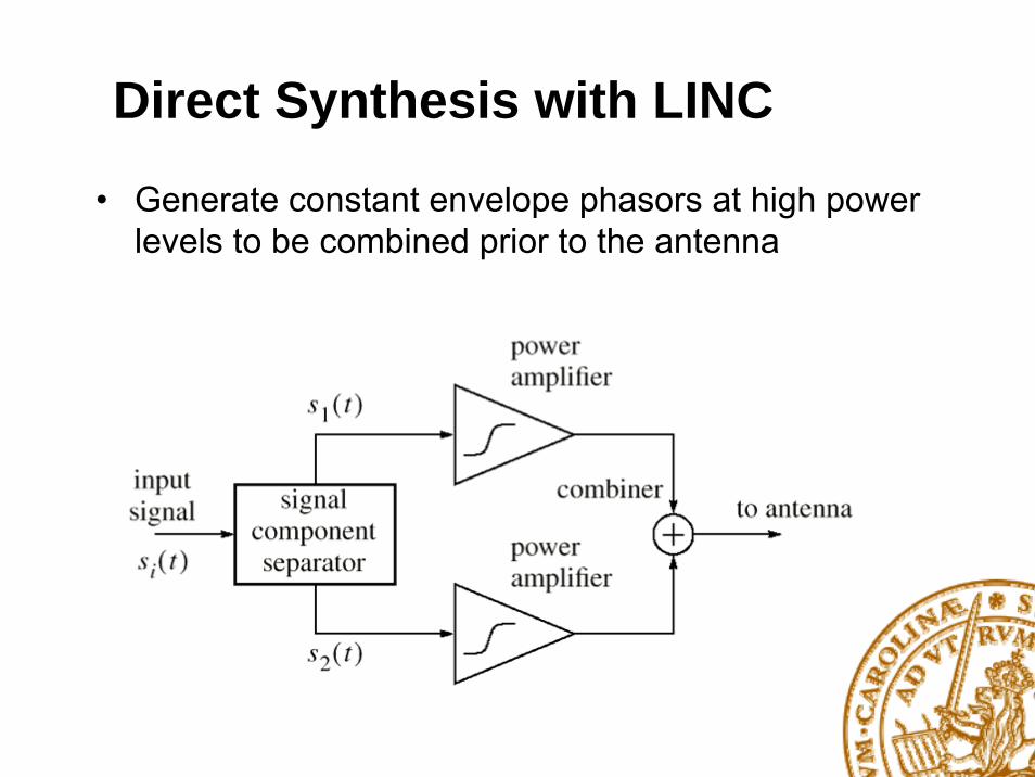
Direct Synthesis with LINC
• Generate constant envelope phasors at high power levels to be combined prior to the antenna

LINC Signal Vector

SCS withBiCMOSCircuit
Bo Shi
• 5V, 100mW• Operates with IF at 200MHz• Standard 0.8um BiCMOS process• Presented at ESSCIRC ’99, JSSC 2000
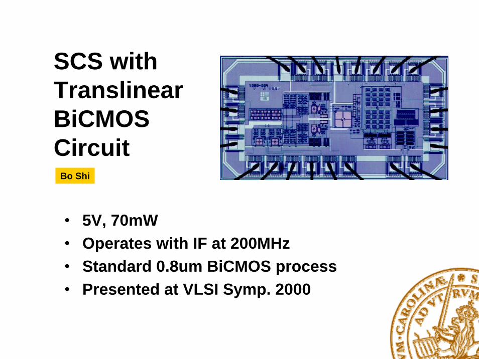
SCS withTranslinearBiCMOSCircuit
Bo Shi
• 5V, 70mW• Operates with IF at 200MHz• Standard 0.8um BiCMOS process• Presented at VLSI Symp. 2000

Experimental Results
55dB
Bo Shi
• PHS signalπ/4 shifted DQPSK
• 384 Kbps

SCS withTranslinearCMOS Circuit
Bo Shi
• 5V, 80mW• Operates with IF at 100MHz• Standard 0.35um CMOS process• Presented at CICC ’01
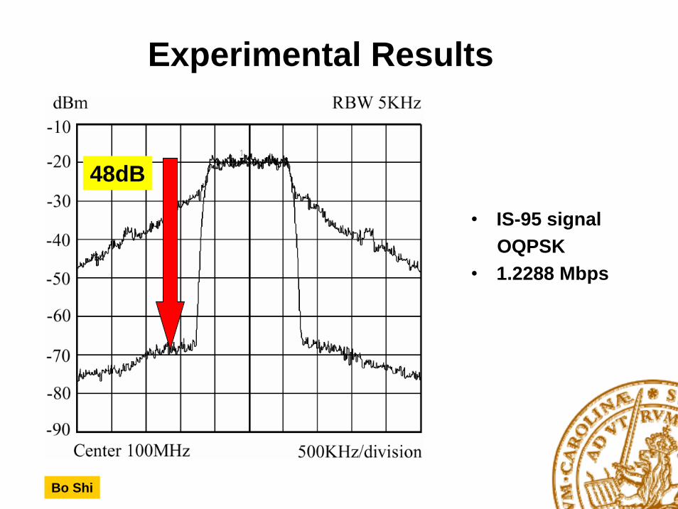
Experimental Results
48dB
Bo Shi
• IS-95 signalOQPSK
• 1.2288 Mbps

2nd Success: CMOS VCO:s• Varactors: Continuous and switched• Phase noise improvements• Low voltage VCO:s• Quadrature VCO:s• High frequencies (presented tomorrow)

CMOS VaractorsPietro Andreani
• MOS device versus ”standard” diode varactor• Strong/weak inversion MOS versus
accumulation/depletion MOS • Embedded in VCO’s with bond wire inductors• ESSCIRC ’98, ISCAS ’99 and 2000, JSSC 2000

A-MOS Varactor
Pietro Andreani
• S. Mattisson ’97• Lee et al., Castello et al.,
VSLI Symposium ’98

Differential Switched Tuning
• Digital coarse frequency tuning• High linearity• Flexibility• Doubled Q compared to
single-ended scheme• IEEE TCAS-II, 2002
b0 b0 b0
C W Cb1 b1 b1
2C 2W 2C
b2 b2 b2
4C 4W 4C
To differentialresonator
Henrik Sjöland

Monolithic CMOS VCO’s with Low Phase Noise (I)
Henrik Sjöland
• High frequency noisefrom tail current is eliminated
• L and C uncritical• designed when he
was at UCLA in Prof. Abidi's group
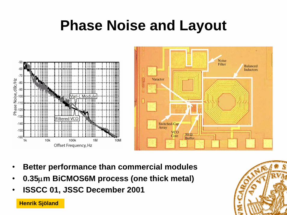
Phase Noise and Layout
• Better performance than commercial modules• 0.35μm BiCMOS6M process (one thick metal)• ISSCC 01, JSSC December 2001
Henrik Sjöland
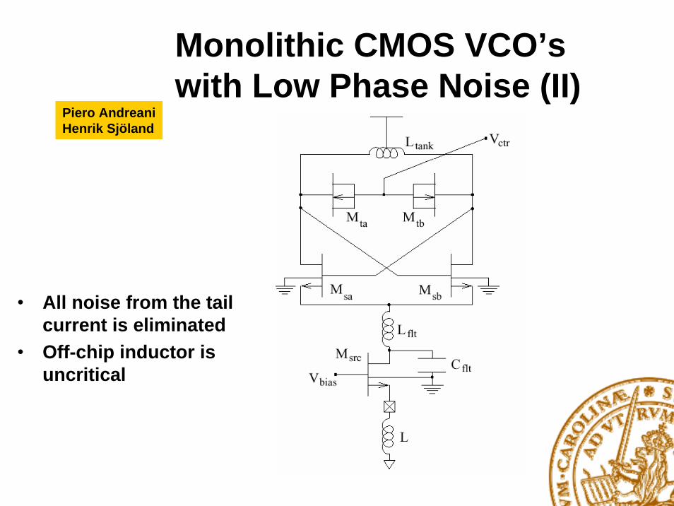
Monolithic CMOS VCO’swith Low Phase Noise (II)
• All noise from the tailcurrent is eliminated
• Off-chip inductor is uncritical
Piero AndreaniHenrik Sjöland

Phase Noise and Layout
Piero AndreaniHenrik Sjöland
• 1.4 V, 9 mA• Digital 0.35um CMOS process• CICC ’01, VLSI Symp. ’01, JSSC ’02

Low Voltage 2.4GHz CMOS VCO
• 1V, 5.5mA, 2.4GHz,15% tuning, -136dBc/Hz @ 3MHz offset, Asia-Pacific ‘02
• 0.7V, 2.8mA, 2.4GHz,13% tuning,-130dBc/Hz @ 3MHz offset, Rawcon ‘02
0.9mm
1.0 mm
Niklas Troedsson
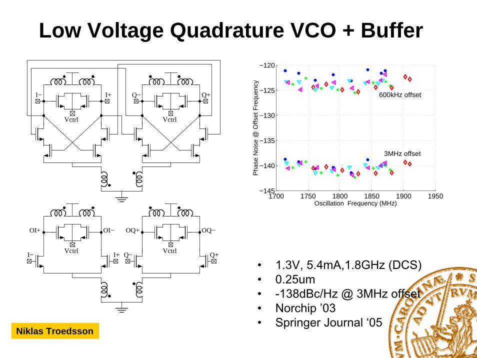
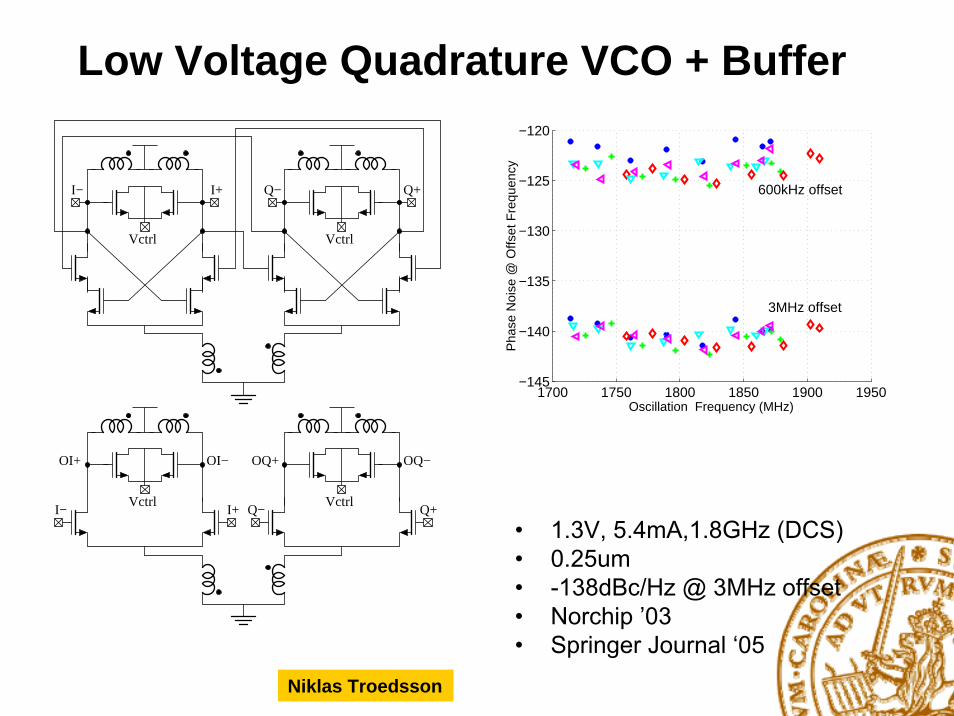
Low Voltage Quadrature VCO + Buffer
• 1.3V, 5.4mA,1.8GHz (DCS)• 0.25um• -138dBc/Hz @ 3MHz offset • Norchip ’03• Springer Journal ‘05
I− I+
Vctrl
OI+
Vctrl
Q− Q+
Vctrl
OQ−OQ+
VctrlI− I+ Q− Q+
OI−
1700 1750 1800 1850 1900 1950−145
−140
−135
−130
−125
−120
Oscillation Frequency (MHz)
Pha
se N
oise
@ O
ffset
Fre
quen
cy
600kHz offset
3MHz offset
Niklas Troedsson
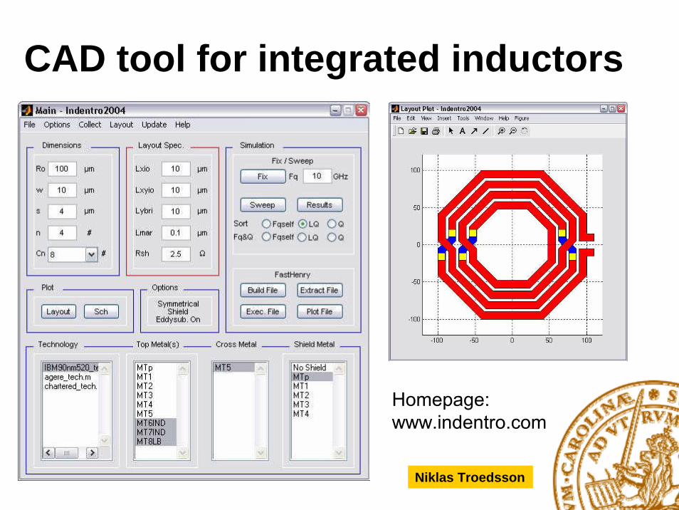
CAD tool for integrated inductors
Homepage:www.indentro.com
Niklas Troedsson

3rd Success: CMOS Receivers
• Linear Frontend• Low Voltage Frontends• Dual Band Frontend• Gm-C Filters

Merged LNA and Mixer forWCDMA Front End
2.7 V, 8 mA, 2.1 GHz3.2 dB NF, -1.5 dBm IIP3< -71 dBm LO @ antennaVLSI Symp. ’01, JSSC ’03 Henrik Sjöland

1V CMOS Bluetooth Front-End
0.25um CMOS 1V, 2.5mA, 2.4GHz14dB Conversion Gain5dB NF-5dBm IIP3, -15dBm CP1ESSCIRC ‘02
Fredrik Tillman

Linearized 1V CMOS front-end
-28 -24 -20 -16 -12
RF input power (dBm)
(dB
m)
-60
-40
-20
0
VLSI Symposium ‘03 Fredrik Tillman

Low Voltage Quadrature Front-End
CMOS chip featuring:• QVCO• VCO Buffers• LNA• Novel Quadrature Passive Mixers
VLSI symposium 2004
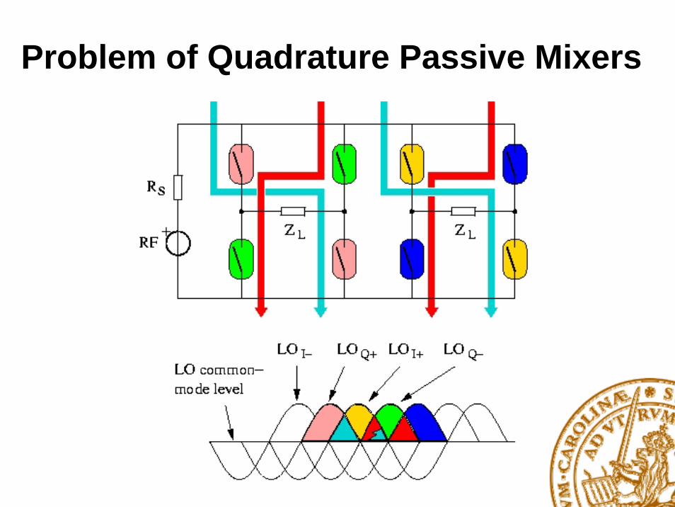
Problem of Quadrature Passive Mixers

New Quadrature Passive Mixer

LNA and Mixer Schematic
Fredrik Tillman
Low Voltage Quadrature VCO + Buffer
• 1.3V, 5.4mA,1.8GHz (DCS)• 0.25um• -138dBc/Hz @ 3MHz offset • Norchip ’03• Springer Journal ‘05
I− I+
Vctrl
OI+
Vctrl
Q− Q+
Vctrl
OQ−OQ+
VctrlI− I+ Q− Q+
OI−
1700 1750 1800 1850 1900 1950−145
−140
−135
−130
−125
−120
Oscillation Frequency (MHz)
Pha
se N
oise
@ O
ffset
Fre
quen
cy
600kHz offset
3MHz offset
Niklas Troedsson
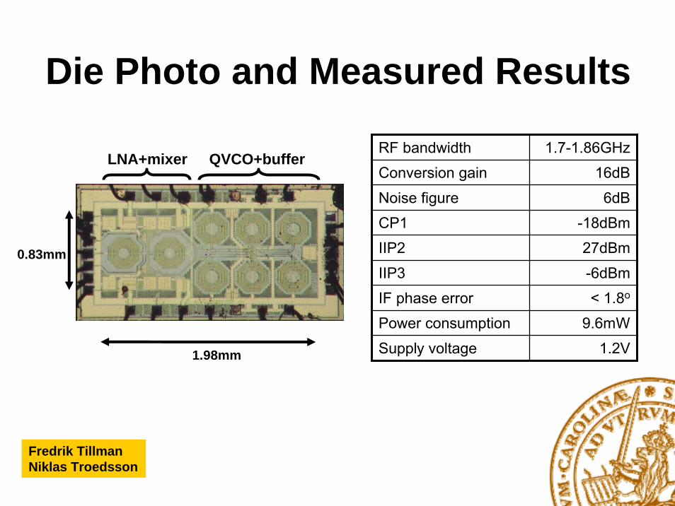
Die Photo and Measured Results
LNA+mixer QVCO+buffer
0.83mm
1.98mm
Fredrik Tillman Niklas Troedsson
RF bandwidth 1.7-1.86GHzConversion gain 16dB
Noise figure 6dBCP1 -18dBmIIP2 27dBm
IIP3 -6dBmIF phase error < 1.8o
Power consumption 9.6mW
Supply voltage 1.2V

Dual Band Front-End
Kittichai Phansathitwong

Chip Photo and Experimental Results
• Chip area of 1.4 mm2
• 0.18um CMOS• 2 GSSG pads
1V 1.8V
2.2GHz 4.0GHz 2.2GHz 4.0GHz
Noise Figure (dB) 3.5 3.0
15
-17
-6
-26
2.4
3.0
Conv. Gain (dB) 10
3.2
11.5
-11
0
-17
15
1-dB comp. (dBm) -11 -17
IIP3 (dBm) 0 -6
S11 (dB) -18 -23
Power Consumption(mW)
2.4 4.7 4.7
Kittichai Phansathitwong

CMOS gm-C IF Filter for Bluetooth
Specifications• 1MHz pass band• 3MHz center frequency• Out-of-band rejection > 40 dB, falling
asymptotically with 60 dB/dec• Group delay ripple less than 1μs• 2.5V, 2.4mA• CICC 2000
Pietro Andreani

Polyphase gm-C ArchitecturePiero Andreani
Lowpass passive stage
Polyphase activegm-C stage
Lowpass activegm-C stage
Transconductor
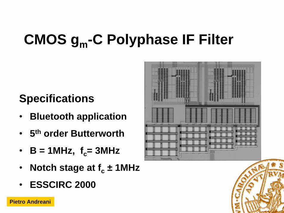
CMOS gm-C Polyphase IF Filter
Specifications• Bluetooth application
• 5th order Butterworth
• B = 1MHz, fc= 3MHz
• Notch stage at fc ± 1MHz
• ESSCIRC 2000Pietro Andreani
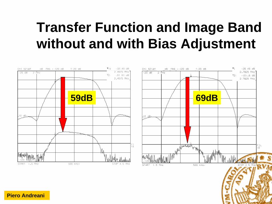
Transfer Function and Image Band without and with Bias Adjustment
Piero Andreani
59dB 69dB
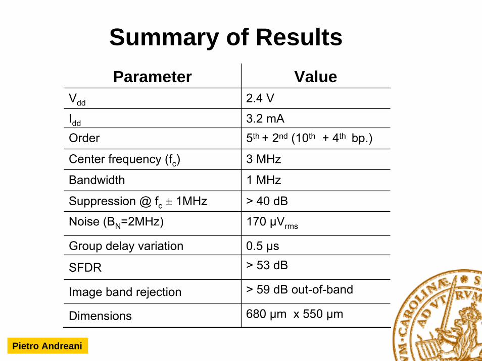
Summary of Results
Pietro Andreani
Parameter ValueVdd 2.4 V
Idd 3.2 mAOrder 5th + 2nd (10th + 4th bp.)
Center frequency (fc) 3 MHz
Suppression @ fc ± 1MHz > 40 dB
Noise (BN=2MHz) 170 µVrms
SFDR > 53 dB
Image band rejection > 59 dB out-of-band
Dimensions 680 µm x 550 µm
Bandwidth 1 MHz
Group delay variation 0.5 µs

4th Success: CMOS at High Frequencies
Measured:• 23GHz QVCO (presented tomorrow)• 8GHz beamforming transmitter
Under fabrication/measurement:• 10GHz quadrature receiver• 60GHz VCO:s• 24GHz beamforming receiver• 23GHz homodyne receiver• 24GHz beamforming transmitter• 60GHz frequency-doubling PA

8GHz beamforming transmitter

Schematics
PA
QVCO and Buffer
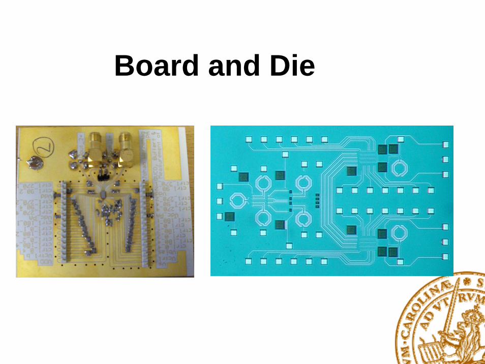
Board and Die

Measurement results
103 104 105 106
-140
-120
-100
-80
-60
-40
-20
Phase noise measurement of three chips and simulation
Phas
e no
ise
(dB
c/H
z)
f (Hz)
chip 1, FOM=180 dBchip 2, FOM=182 dBchip 3, FOM=181 dBSimulation, FOM=181 dB
7.7 7.8 7.9 8 8.1 8.2-7
-6
-5
-4
-3
-2
-1
Maximum output power
f (GHz)
Out
put p
ower
(dB
m)
chip 1, tuning range: 4.5%chip 2, tuning range: 4.9%chip 3, tuning range: 4.6%
0 10 20 30 40 50 60 70 80 900
10
20
30
40
50
60
70
80
90
Theoretical phase offset
Mea
sure
d ph
ase
offs
et
chip 1chip 2chip 3
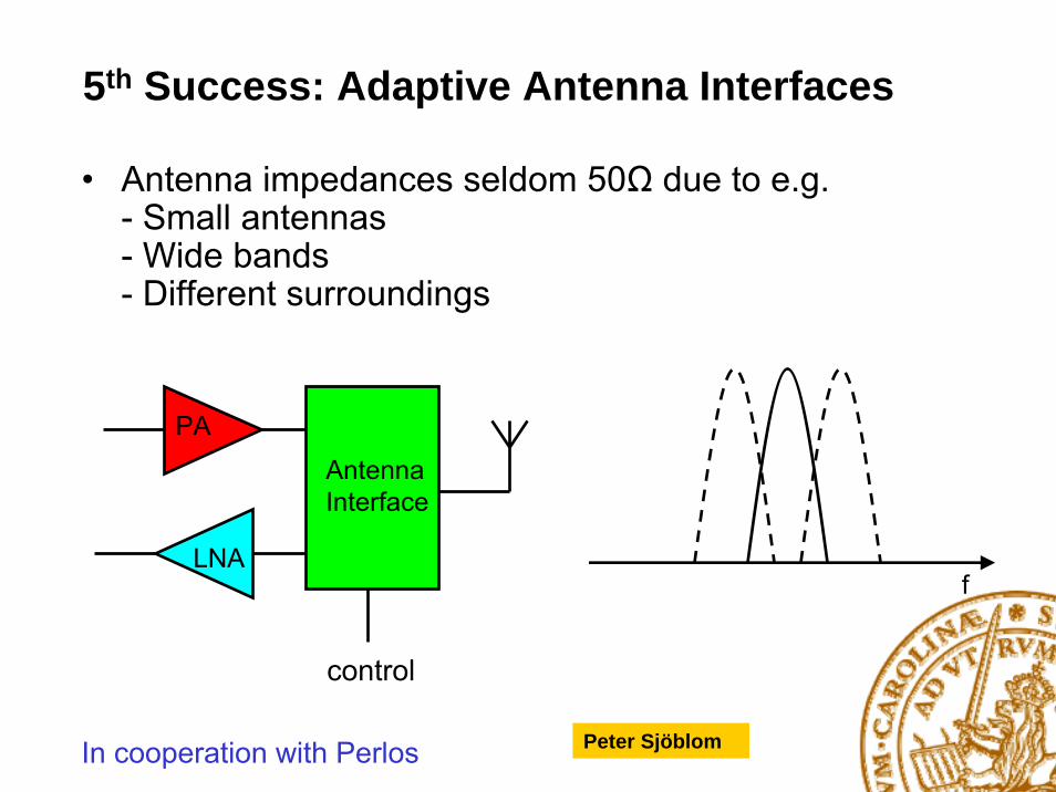
5th Success: Adaptive Antenna Interfaces
• Antenna impedances seldom 50Ω due to e.g.- Small antennas- Wide bands- Different surroundings
In cooperation with Perlos
AntennaInterface
PA
LNAf
control
Peter Sjöblom

Matching Networks for DVB-H
• TV in your PDA/Phone• 470-702MHz, wide band, low frequency• Reconfigurable matching• 130nm UMC CMOS
Peter Sjöblom

Q and Range of Switched C
• Probe measurements• To appear in TCAS-II
Peter Sjöblom

Mismatch and Matching Domain
• Measured data:- Two mismatch networks, HighZ and LowZ- Impedance Tuing Unit
Peter Sjöblom

Measured Noise Improvement
Low Z High Z
Peter Sjöblom Fredrik Ahlberg
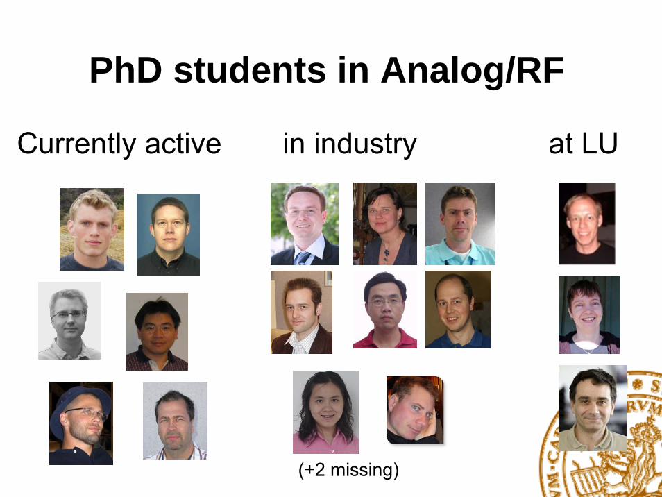
PhD students in Analog/RF
Currently active in industry at LU
(+2 missing)
Conclusions• Many successful RF projects• Lots of RF CMOS circuits designed
(Not all mentioned today)• Skilled researchers produced• Made possible by cooperation in the Centre• Hope to continue this success!