chapter 2: memory hierarchy design - cs.ucf.edudcm/teaching/cda5106-fall2015/slides/ch2.pdf · 38...
TRANSCRIPT
1
Chapter 2
Memory Hierarchy Design
Computer Architecture A Quantitative Approach, Fifth Edition
Copyright © 2012, Elsevier Inc. All rights reserved.
2
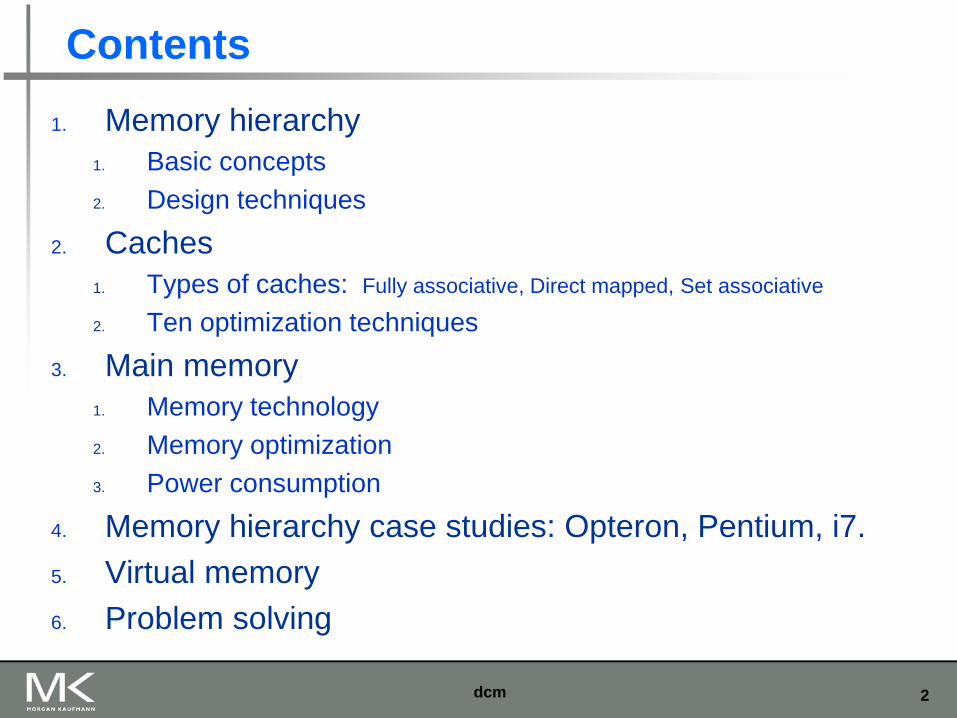
Contents
1. Memory hierarchy
1. Basic concepts
2. Design techniques
2. Caches
1. Types of caches: Fully associative, Direct mapped, Set associative
2. Ten optimization techniques
3. Main memory
1. Memory technology
2. Memory optimization
3. Power consumption
4. Memory hierarchy case studies: Opteron, Pentium, i7.
5. Virtual memory
6. Problem solving
dcm
3
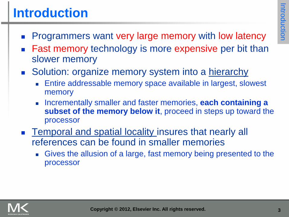
Introduction
Programmers want very large memory with low latency
Fast memory technology is more expensive per bit than slower memory
Solution: organize memory system into a hierarchy Entire addressable memory space available in largest, slowest
memory
Incrementally smaller and faster memories, each containing a subset of the memory below it, proceed in steps up toward the processor
Temporal and spatial locality insures that nearly all references can be found in smaller memories Gives the allusion of a large, fast memory being presented to the
processor
Intro
ductio
n
Copyright © 2012, Elsevier Inc. All rights reserved.
4
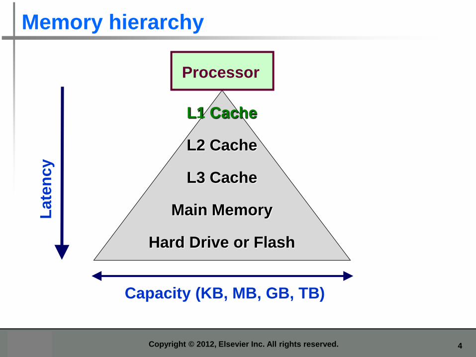
Memory hierarchy
Processor
Late
ncy
L1 Cache
L2 Cache
L3 Cache
Main Memory
Hard Drive or Flash
Capacity (KB, MB, GB, TB)
Copyright © 2012, Elsevier Inc. All rights reserved.
5
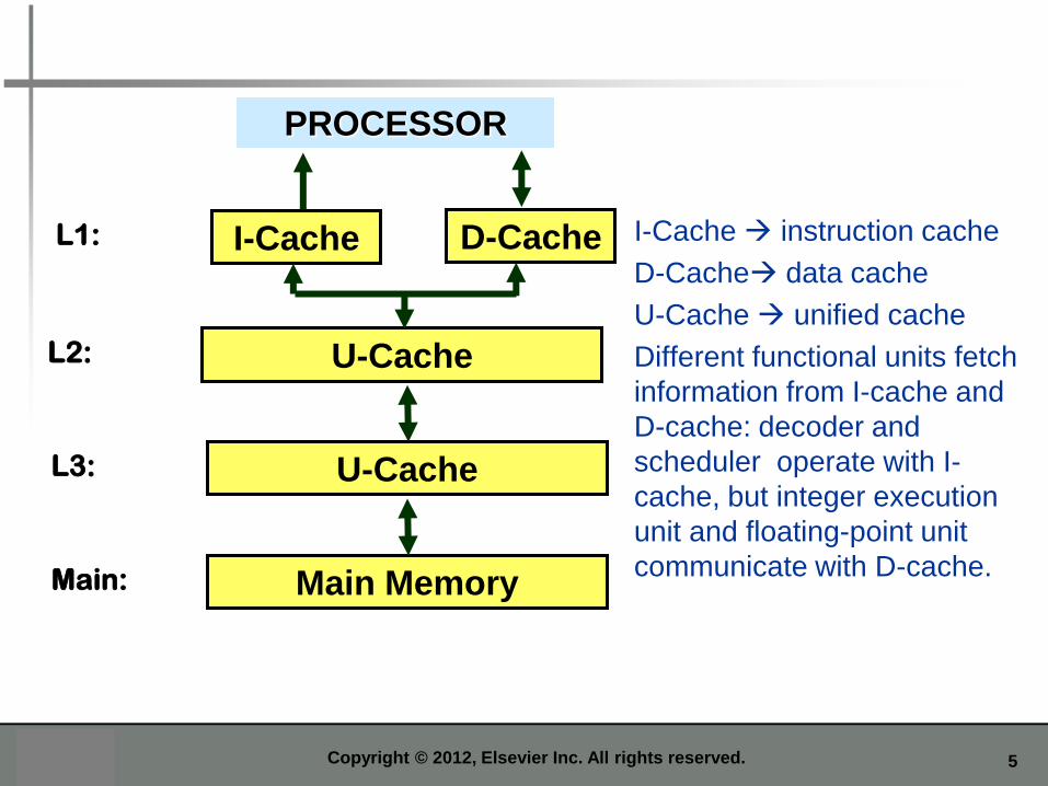
PROCESSOR
I-Cache D-Cache L1:
U-Cache L2:
U-Cache L3:
Main Memory Main:
I-Cache instruction cache
D-Cache data cache
U-Cache unified cache
Different functional units fetch
information from I-cache and
D-cache: decoder and
scheduler operate with I-
cache, but integer execution
unit and floating-point unit
communicate with D-cache.
Copyright © 2012, Elsevier Inc. All rights reserved.
6
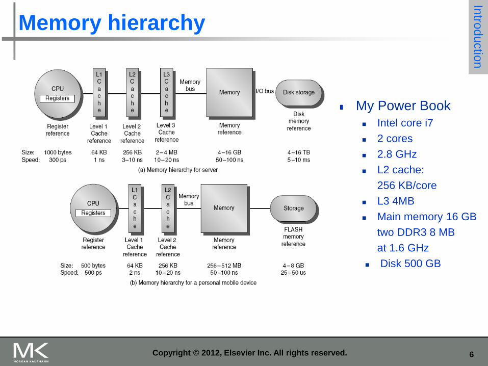
Memory hierarchy
My Power Book
Intel core i7
2 cores
2.8 GHz
L2 cache:
256 KB/core
L3 4MB
Main memory 16 GB
two DDR3 8 MB
at 1.6 GHz
Disk 500 GB
Copyright © 2012, Elsevier Inc. All rights reserved.
Intro
ductio
n
7
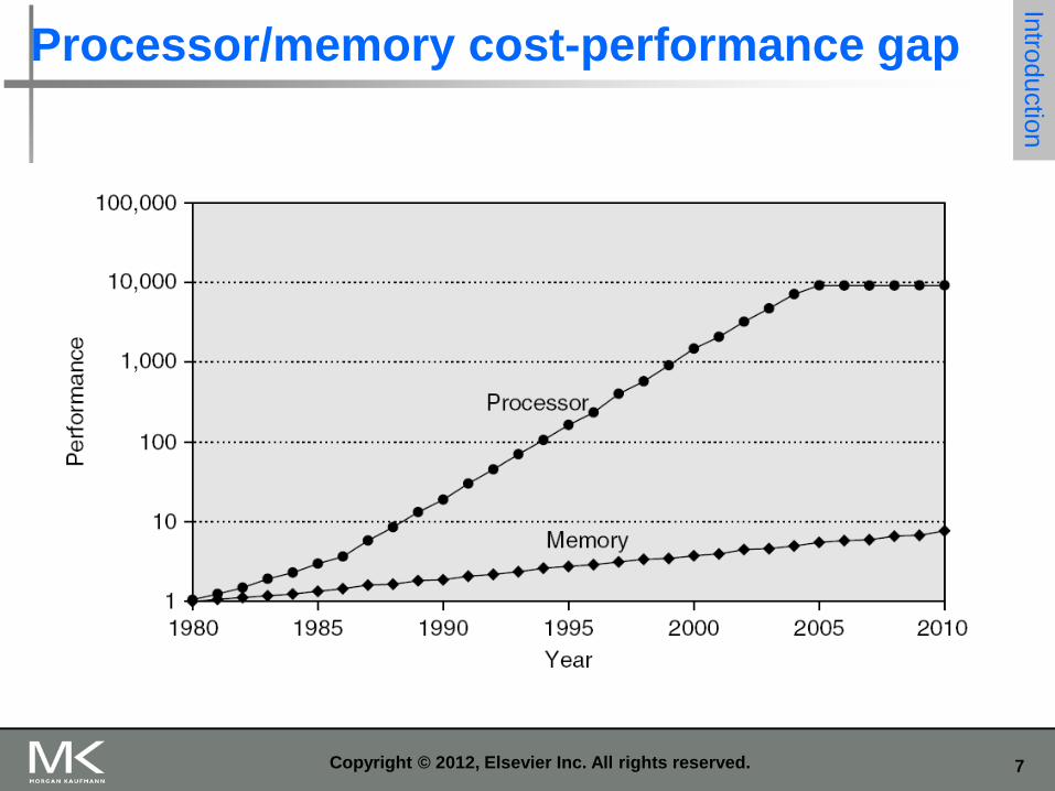
Processor/memory cost-performance gap In
troductio
n
Copyright © 2012, Elsevier Inc. All rights reserved.
8
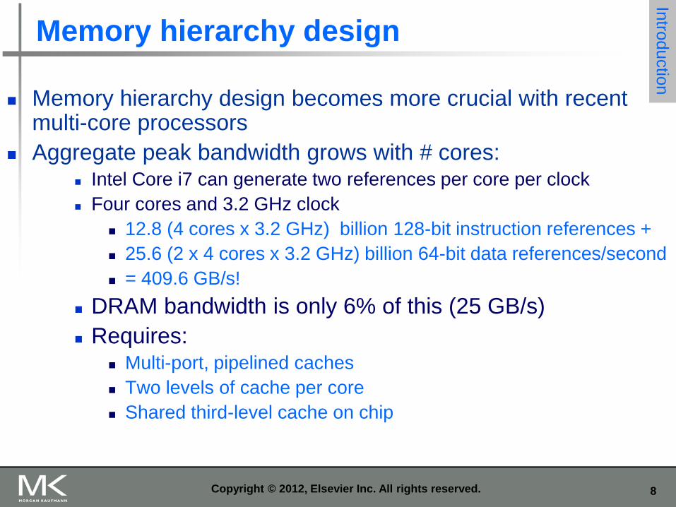
Memory hierarchy design
Memory hierarchy design becomes more crucial with recent multi-core processors
Aggregate peak bandwidth grows with # cores: Intel Core i7 can generate two references per core per clock
Four cores and 3.2 GHz clock
12.8 (4 cores x 3.2 GHz) billion 128-bit instruction references +
25.6 (2 x 4 cores x 3.2 GHz) billion 64-bit data references/second
= 409.6 GB/s!
DRAM bandwidth is only 6% of this (25 GB/s)
Requires: Multi-port, pipelined caches
Two levels of cache per core
Shared third-level cache on chip
Intro
ductio
n
Copyright © 2012, Elsevier Inc. All rights reserved.
9
Performance and power
High-end microprocessors have >10 MB on-chip cache
The cache consumes a large amount of area and power budget
Intro
ductio
n
Copyright © 2012, Elsevier Inc. All rights reserved.
10
Memory hierarchy basics
When a word is not found in the cache, a miss occurs.
In case of a miss fetch word from lower level in hierarchy higher latency reference
lower level may be: another cache
the main memory
fetch the entire block consisting of several words Takes advantage of spatial locality
place block into cache in any location within its set, determined by address block address MOD number of sets
Intro
ductio
n
Copyright © 2012, Elsevier Inc. All rights reserved.
11
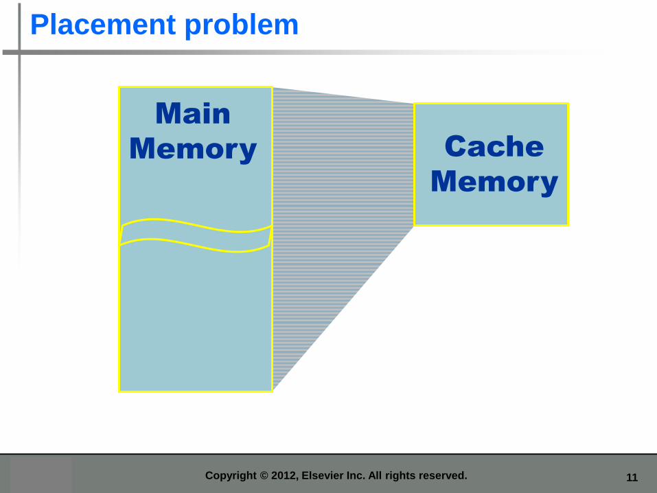
Placement problem
Main
Memory Cache
Memory
Copyright © 2012, Elsevier Inc. All rights reserved.
12
Placement policies
Main memory has a much larger capacity than cache.
Mapping between main and cache memories.
Where to put a block in cache
Copyright © 2012, Elsevier Inc. All rights reserved.
13
0
1
2
3
4
5
6
7
8
9
10
11
12
13
14
15
16
17
18
19
20
21
22
23
24
25
26
27
28
29
30
31
Memory
Blo
ck n
um
be
r
0
1
2
3
4
5
6
7
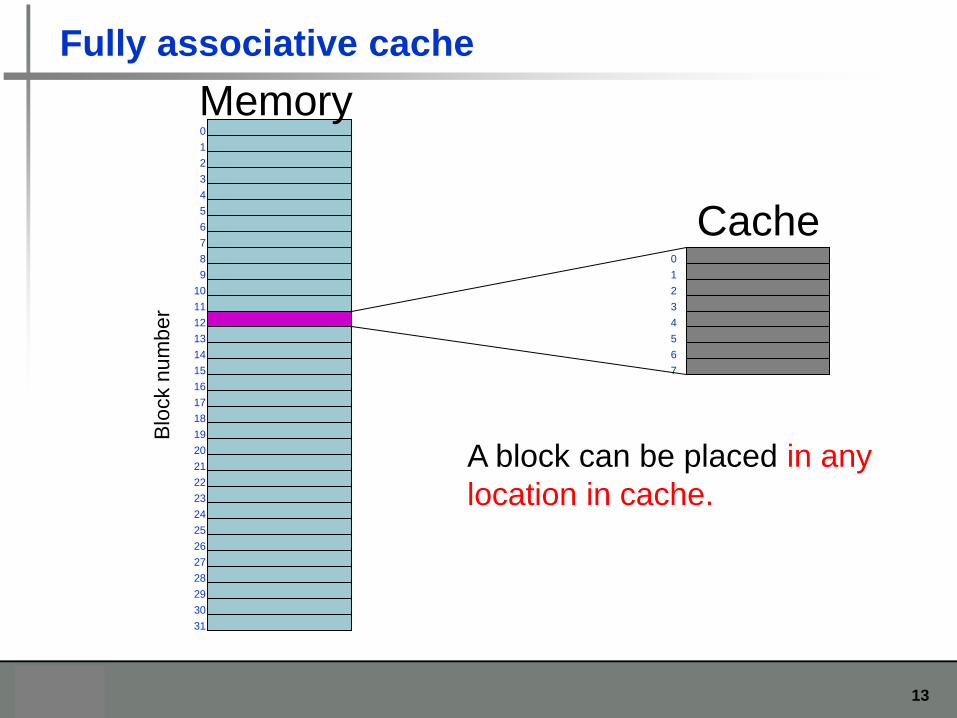
Fully associative cache
A block can be placed in any
location in cache.
Cache
14
0
1
2
3
4
5
6
7
8
9
10
11
12
13
14
15
16
17
18
19
20
21
22
23
24
25
26
27
28
29
30
31
Memory
Blo
ck n
um
be
r
0
1
2
3
4
5
6
7
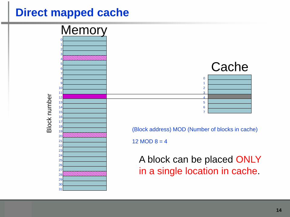
Direct mapped cache
(Block address) MOD (Number of blocks in cache)
12 MOD 8 = 4
A block can be placed ONLY
in a single location in cache.
Cache
15
0
1
2
3
4
5
6
7
8
9
10
11
12
13
14
15
16
17
18
19
20
21
22
23
24
25
26
27
28
29
30
31
Memory
Blo
ck n
um
be
r
0
1
2
3
4
5
6
7
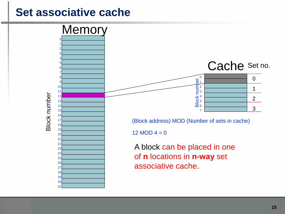
Set associative cache
(Block address) MOD (Number of sets in cache)
12 MOD 4 = 0
0
1
2
3
Set no.
Blo
ck n
um
ber
A block can be placed in one
of n locations in n-way set
associative cache.
Cache
16
Memory hierarchy basics
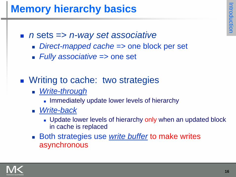
n sets => n-way set associative Direct-mapped cache => one block per set
Fully associative => one set
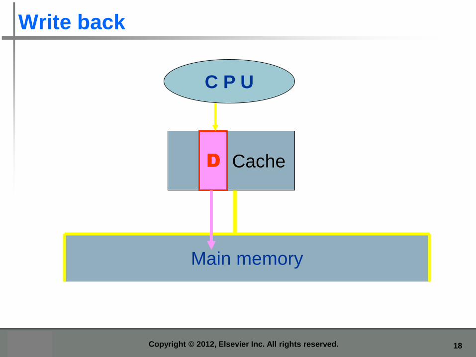
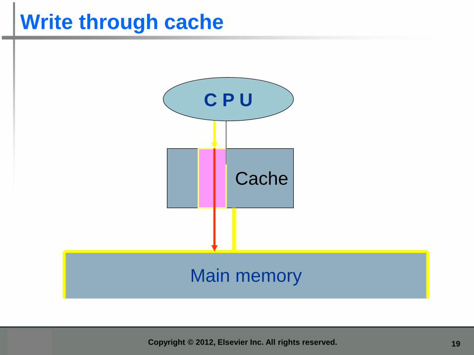
Writing to cache: two strategies Write-through
Immediately update lower levels of hierarchy
Write-back Update lower levels of hierarchy only when an updated block
in cache is replaced
Both strategies use write buffer to make writes asynchronous
Intro
ductio
n
17
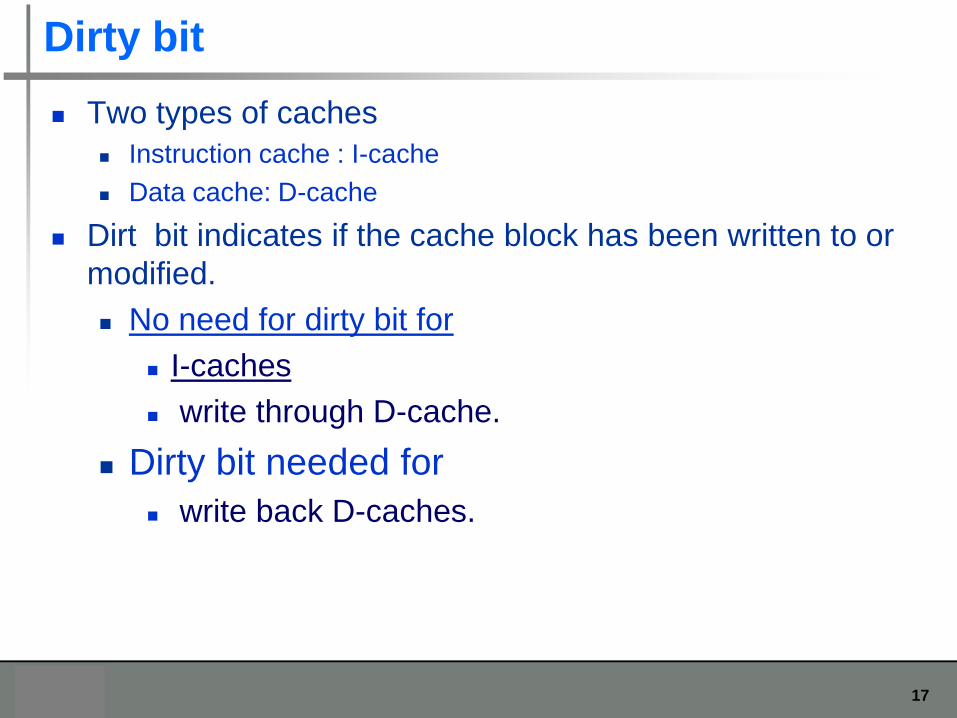
Dirty bit
Two types of caches
Instruction cache : I-cache
Data cache: D-cache
Dirt bit indicates if the cache block has been written to or
modified.
No need for dirty bit for
I-caches
write through D-cache.
Dirty bit needed for
write back D-caches.
18
Write back
C P U
Main memory
Cache D
Copyright © 2012, Elsevier Inc. All rights reserved.
19
Write through cache
C P U
Main memory
Cache
Copyright © 2012, Elsevier Inc. All rights reserved.
20
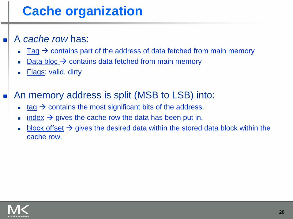
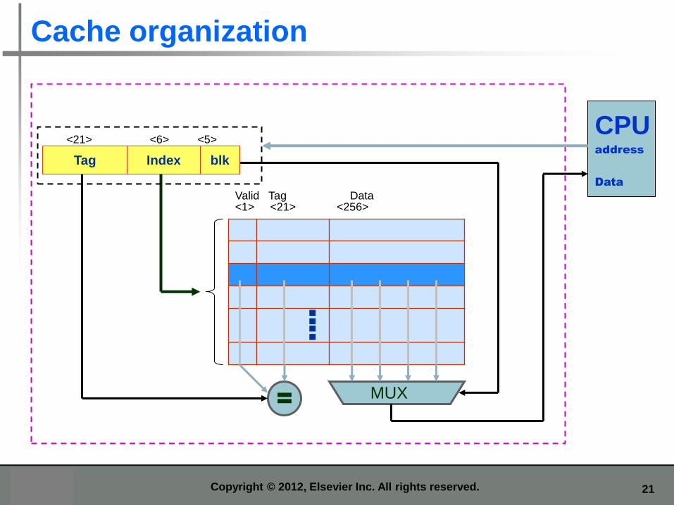
Cache organization
A cache row has: Tag contains part of the address of data fetched from main memory
Data bloc contains data fetched from main memory
Flags: valid, dirty
An memory address is split (MSB to LSB) into: tag contains the most significant bits of the address.
index gives the cache row the data has been put in.
block offset gives the desired data within the stored data block within the
cache row.
21
Cache organization
: :
<1> <21> <256> Valid Tag Data
CPU address
Data
= MUX
Tag Index blk
<21> <6> <5>
Copyright © 2012, Elsevier Inc. All rights reserved.
22
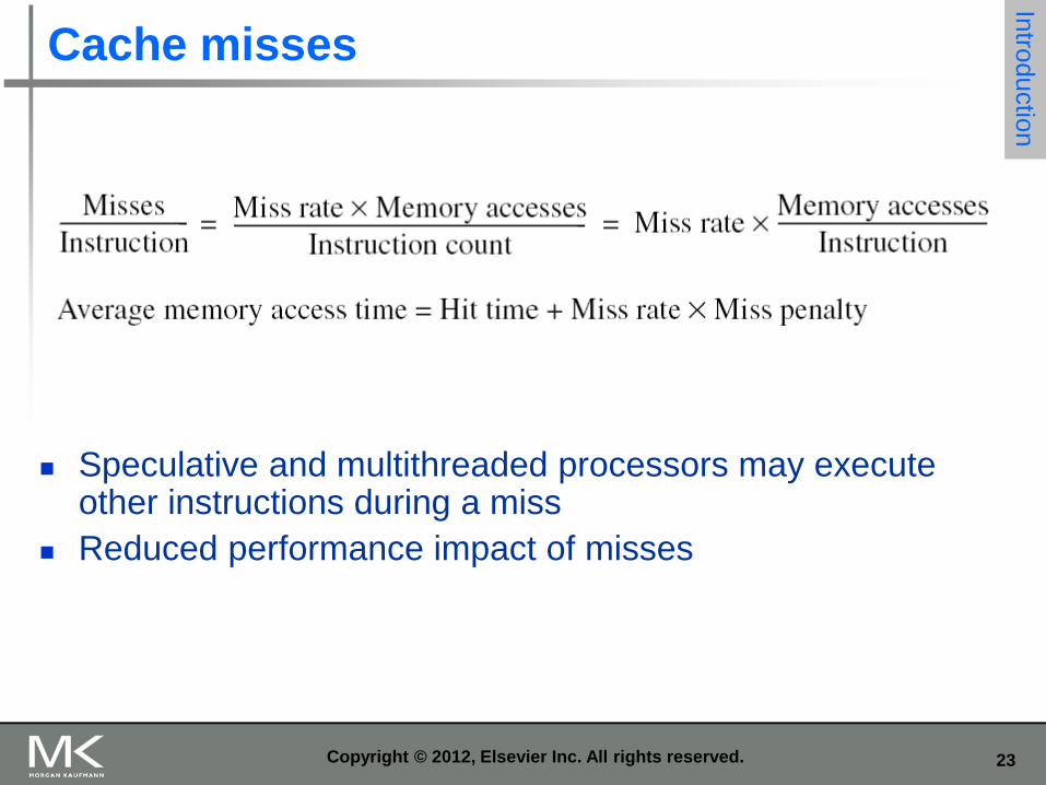
Cache misses
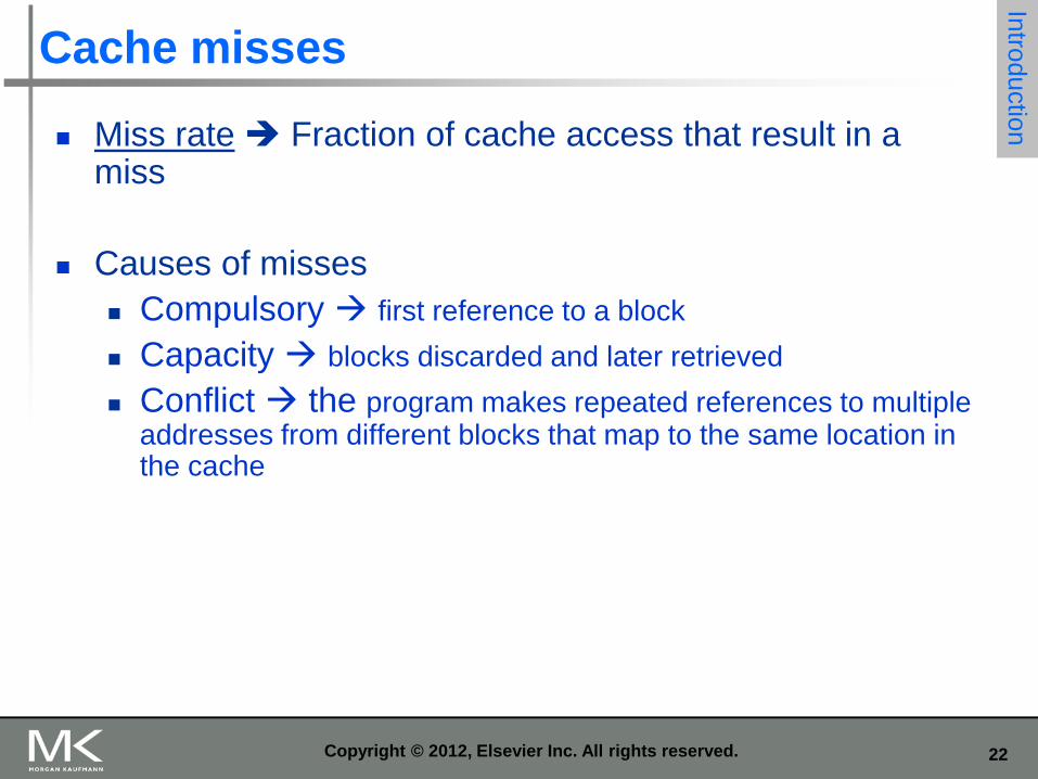
Miss rate Fraction of cache access that result in a miss
Causes of misses
Compulsory first reference to a block
Capacity blocks discarded and later retrieved
Conflict the program makes repeated references to multiple addresses from different blocks that map to the same location in the cache
Intro
ductio
n
Copyright © 2012, Elsevier Inc. All rights reserved.
23
Speculative and multithreaded processors may execute
other instructions during a miss
Reduced performance impact of misses
Cache misses In
troductio
n
Copyright © 2012, Elsevier Inc. All rights reserved.
24
Basic cache optimizations techniques
Larger block size Reduces compulsory misses
Increases capacity and conflict misses, increases miss penalty
Larger total cache capacity to reduce miss rate Increases hit time, increases power consumption
Higher associativity Reduces conflict misses
Increases hit time, increases power consumption
Higher number of cache levels Reduces overall memory access time
Give priority to read misses over writes Reduces miss penalty
Avoid address translation in cache indexing Reduces hit time
Intro
ductio
n
Copyright © 2012, Elsevier Inc. All rights reserved.
25
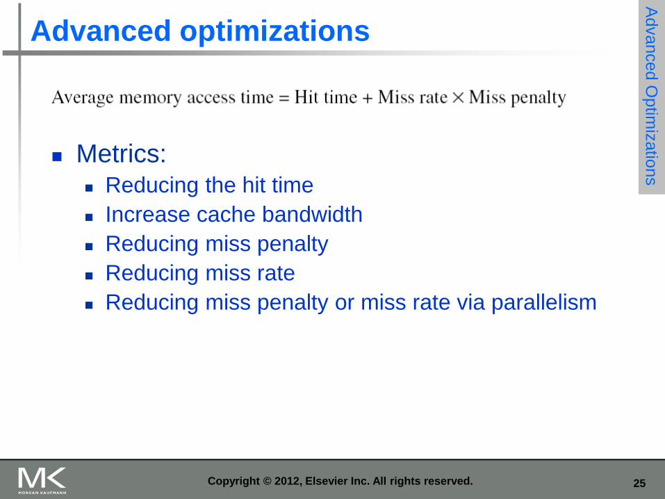
Advanced optimizations
Metrics: Reducing the hit time
Increase cache bandwidth
Reducing miss penalty
Reducing miss rate
Reducing miss penalty or miss rate via parallelism
Advanced O
ptim
izatio
ns
Copyright © 2012, Elsevier Inc. All rights reserved.
26
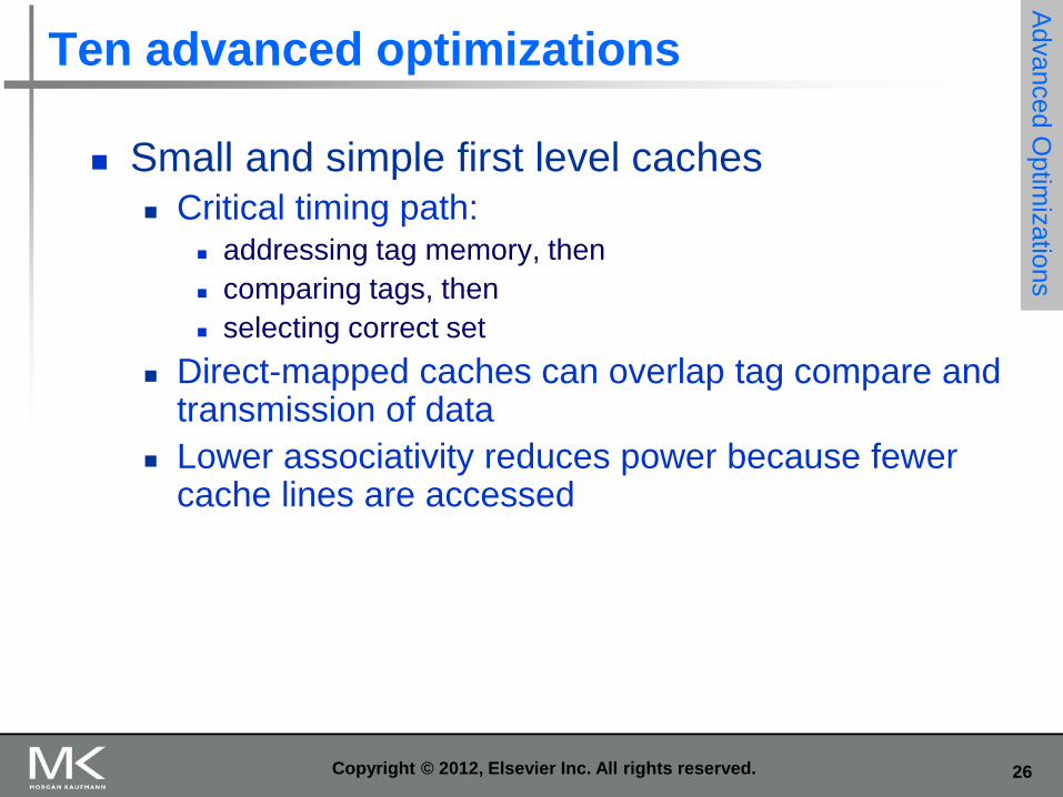
Ten advanced optimizations
Small and simple first level caches Critical timing path:
addressing tag memory, then
comparing tags, then
selecting correct set
Direct-mapped caches can overlap tag compare and transmission of data
Lower associativity reduces power because fewer cache lines are accessed
Advanced O
ptim
izatio
ns
Copyright © 2012, Elsevier Inc. All rights reserved.
27
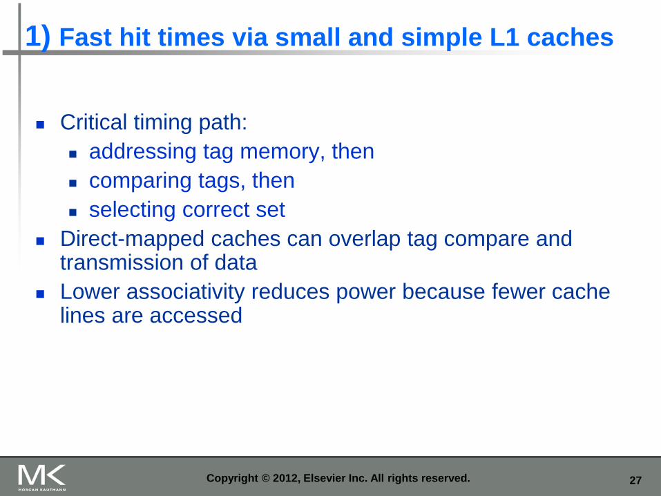
1) Fast hit times via small and simple L1 caches
Critical timing path:
addressing tag memory, then
comparing tags, then
selecting correct set
Direct-mapped caches can overlap tag compare and transmission of data
Lower associativity reduces power because fewer cache lines are accessed
Copyright © 2012, Elsevier Inc. All rights reserved.
28
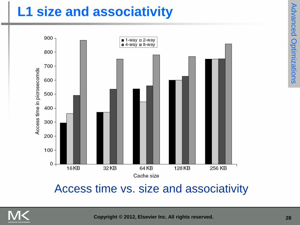
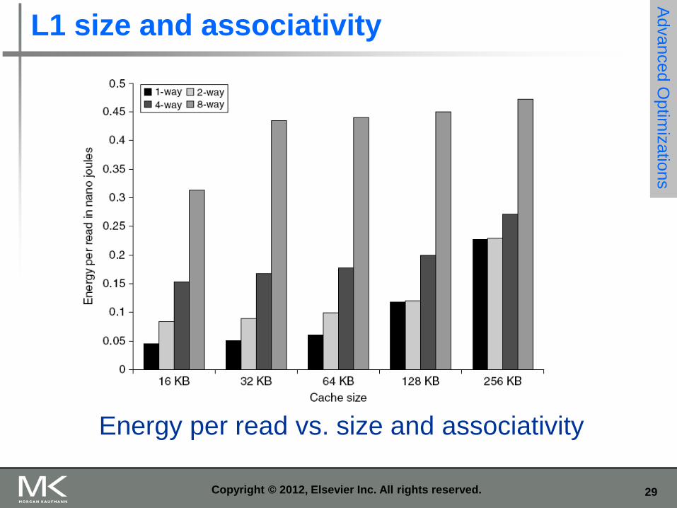
L1 size and associativity
Access time vs. size and associativity
Advanced O
ptim
izatio
ns
Copyright © 2012, Elsevier Inc. All rights reserved.
29
L1 size and associativity
Energy per read vs. size and associativity
Advanced O
ptim
izatio
ns
Copyright © 2012, Elsevier Inc. All rights reserved.
30
2) Fast hit times via way prediction
How to combine fast hit time of Direct Mapped and have the lower
conflict misses of 2-way SA cache?
Way prediction: keep extra bits in cache to predict the “way,” or block
within the set, of next cache access.
Multiplexor is set early to select desired block, only 1 tag comparison
performed that clock cycle in parallel with reading the cache data
Miss 1st check other blocks for matches in next clock cycle
Drawback: CPU pipeline is hard if hit takes 1 or 2 cycles
Prediction accuracy
> 90% for two-way
> 80% for four-way
I-cache has better accuracy than D-cache
First used on MIPS R10000 in mid-90s. Used on ARM Cortex-A8
Extend to predict block as well.
“Way selection” increases mis-prediction penalty
Advanced O
ptim
izatio
ns
Copyright © 2012, Elsevier Inc. All rights reserved.
31
3) Increase cache bandwidth by pipelining
Pipelining improves bandwidth, but higher latency
More clock cycles between the issue of the load and the use of data
Examples: Pentium: 1 cycle
Pentium Pro – Pentium III: 2 cycles
Pentium 4 – Core i7: 4 cycles
Increases branch mis-prediction penalty
Makes it easier to increase associativity
Advanced O
ptim
izatio
ns
Copyright © 2012, Elsevier Inc. All rights reserved.
32
4. Increase cache bandwidth: non-blocking caches
Pipelined processors allow out-of-order execution. The processor should not stall during a data cache miss.
Non-blocking cache or lockup-free cache allow data cache to continue to supply cache hits during a miss Requires additional bits on registers or out-of-order execution
Requires multi-bank memories
“hit under miss” reduces the effective miss penalty by working during miss vs. ignoring CPU requests
“hit under multiple miss” or “miss under miss” may further lower the effective miss penalty by overlapping multiple misses Significantly increases the complexity of the cache controller as
there can be multiple outstanding memory accesses
Requires multiple memory banks (otherwise cannot support)
Pentium Pro allows 4 outstanding memory misses
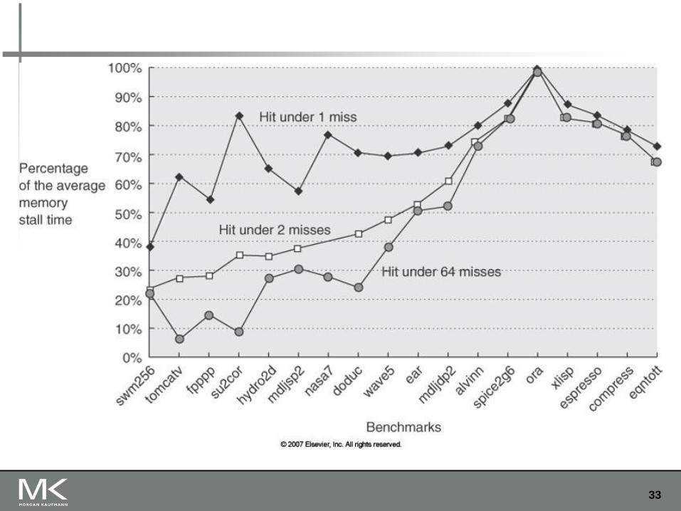
33
34
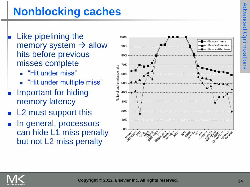
Nonblocking caches
Like pipelining the memory system allow hits before previous misses complete “Hit under miss”
“Hit under multiple miss”
Important for hiding memory latency
L2 must support this
In general, processors can hide L1 miss penalty but not L2 miss penalty
Advanced O
ptim
izatio
ns
Copyright © 2012, Elsevier Inc. All rights reserved.
35 http://csg.csail.mit.edu/6.S078
36
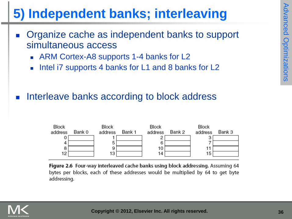
5) Independent banks; interleaving
Organize cache as independent banks to support simultaneous access ARM Cortex-A8 supports 1-4 banks for L2
Intel i7 supports 4 banks for L1 and 8 banks for L2
Interleave banks according to block address
Advanced O
ptim
izatio
ns
Copyright © 2012, Elsevier Inc. All rights reserved.
37
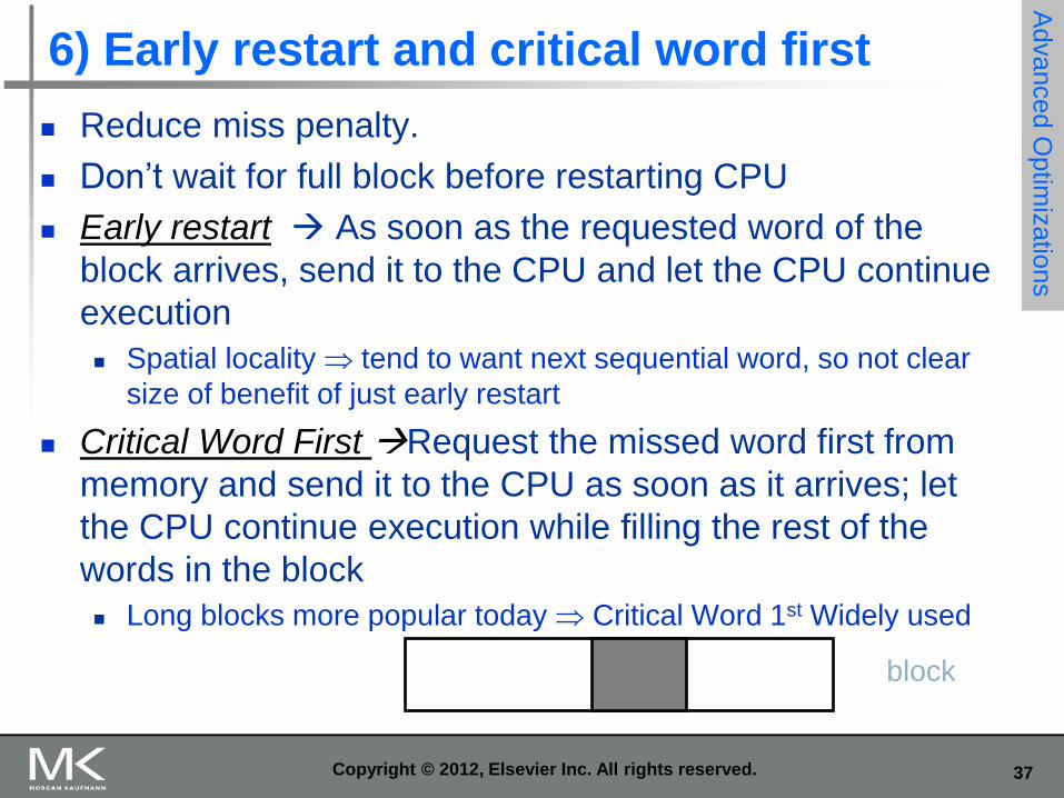
6) Early restart and critical word first
Reduce miss penalty.
Don’t wait for full block before restarting CPU
Early restart As soon as the requested word of the
block arrives, send it to the CPU and let the CPU continue
execution
Spatial locality tend to want next sequential word, so not clear
size of benefit of just early restart
Critical Word First Request the missed word first from
memory and send it to the CPU as soon as it arrives; let
the CPU continue execution while filling the rest of the
words in the block
Long blocks more popular today Critical Word 1st Widely used
Advanced O
ptim
izatio
ns
Copyright © 2012, Elsevier Inc. All rights reserved.
block
38
7. Merging write buffer to reduce miss penalty
Write buffer to allow processor to continue while waiting
to write to memory
If buffer contains modified blocks, the addresses can be
checked to see if address of new data matches the
address of a valid write buffer entry
If so, new data are combined with that entry
Increases block size of write for write-through cache of
writes to sequential words, bytes since multiword writes
more efficient to memory
The Sun T1 (Niagara) processor, among many others,
uses write merging
39
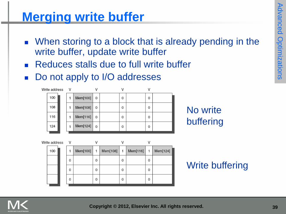
Merging write buffer
When storing to a block that is already pending in the write buffer, update write buffer
Reduces stalls due to full write buffer
Do not apply to I/O addresses
Advanced O
ptim
izatio
ns
No write
buffering
Write buffering
Copyright © 2012, Elsevier Inc. All rights reserved.
40
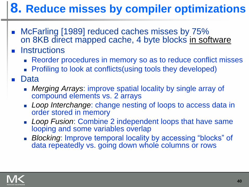
8. Reduce misses by compiler optimizations
McFarling [1989] reduced caches misses by 75% on 8KB direct mapped cache, 4 byte blocks in software
Instructions Reorder procedures in memory so as to reduce conflict misses
Profiling to look at conflicts(using tools they developed)
Data Merging Arrays: improve spatial locality by single array of
compound elements vs. 2 arrays
Loop Interchange: change nesting of loops to access data in order stored in memory
Loop Fusion: Combine 2 independent loops that have same looping and some variables overlap
Blocking: Improve temporal locality by accessing “blocks” of data repeatedly vs. going down whole columns or rows
41
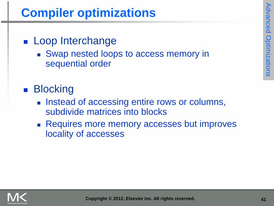
Compiler optimizations
Loop Interchange Swap nested loops to access memory in
sequential order
Blocking Instead of accessing entire rows or columns,
subdivide matrices into blocks
Requires more memory accesses but improves locality of accesses
Advanced O
ptim
izatio
ns
Copyright © 2012, Elsevier Inc. All rights reserved.
42
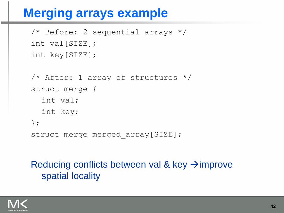
Merging arrays example
/* Before: 2 sequential arrays */
int val[SIZE];
int key[SIZE];
/* After: 1 array of structures */
struct merge {
int val;
int key;
};
struct merge merged_array[SIZE];
Reducing conflicts between val & key improve
spatial locality
43
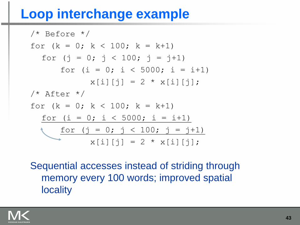
Loop interchange example
/* Before */
for (k = 0; k < 100; k = k+1)
for (j = 0; j < 100; j = j+1)
for (i = 0; i < 5000; i = i+1)
x[i][j] = 2 * x[i][j];
/* After */
for (k = 0; k < 100; k = k+1)
for (i = 0; i < 5000; i = i+1)
for (j = 0; j < 100; j = j+1)
x[i][j] = 2 * x[i][j];
Sequential accesses instead of striding through
memory every 100 words; improved spatial
locality
44
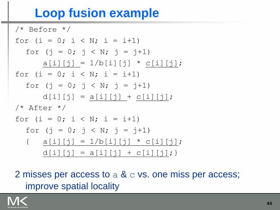
Loop fusion example /* Before */
for (i = 0; i < N; i = i+1)
for (j = 0; j < N; j = j+1)
a[i][j] = 1/b[i][j] * c[i][j];
for (i = 0; i < N; i = i+1)
for (j = 0; j < N; j = j+1)
d[i][j] = a[i][j] + c[i][j];
/* After */
for (i = 0; i < N; i = i+1)
for (j = 0; j < N; j = j+1)
{ a[i][j] = 1/b[i][j] * c[i][j];
d[i][j] = a[i][j] + c[i][j];}
2 misses per access to a & c vs. one miss per access;
improve spatial locality
45
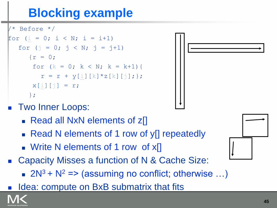
Blocking example /* Before */
for (i = 0; i < N; i = i+1)
for (j = 0; j < N; j = j+1)
{r = 0;
for (k = 0; k < N; k = k+1){
r = r + y[i][k]*z[k][j];};
x[i][j] = r;
};
Two Inner Loops:
Read all NxN elements of z[]
Read N elements of 1 row of y[] repeatedly
Write N elements of 1 row of x[]
Capacity Misses a function of N & Cache Size:
2N3 + N2 => (assuming no conflict; otherwise …)
Idea: compute on BxB submatrix that fits
46
Blocking example
/* After */
for (jj = 0; jj < N; jj = jj+B)
for (kk = 0; kk < N; kk = kk+B)
for (i = 0; i < N; i = i+1)
for (j = jj; j < min(jj+B-1,N); j = j+1)
{r = 0;
for (k = kk; k < min(kk+B-1,N); k = k+1) {
r = r + y[i][k]*z[k][j];};
x[i][j] = x[i][j] + r;
};
B called Blocking Factor
Capacity Misses from 2N3 + N2 to 2N3/B +N2
Conflict Misses Too?

47
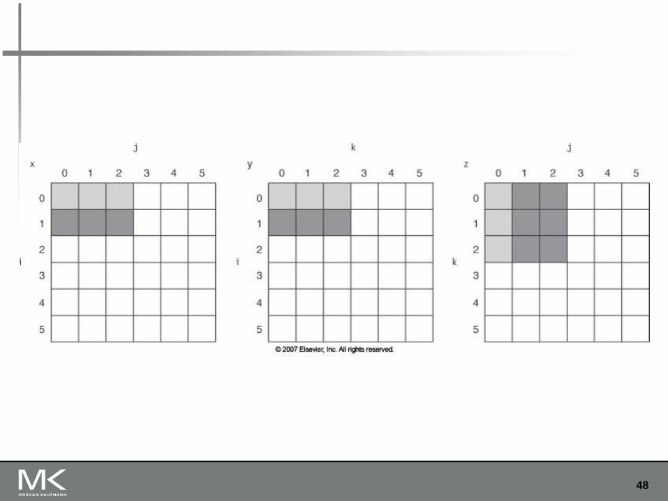
Snapshot of arrays x,y,z when N=6 and i =1
The age of access to the array elements is indicated by shade.
White not yet touched
Light older access
Dark new access
In the “before” algorithm the elements of y and z are read repeatedly to
calculate x. Compare with the next slide which shows the “after” access
patterns. Indexes, I, j, and k are shown along the rows and columns.
48
49
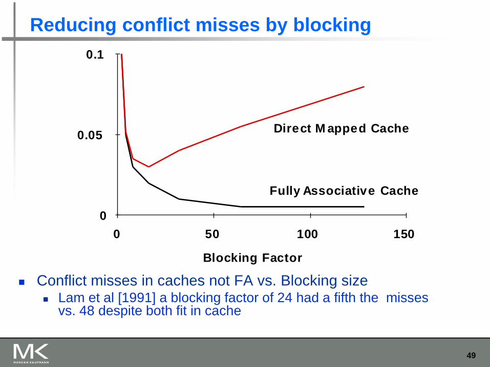
Reducing conflict misses by blocking
Conflict misses in caches not FA vs. Blocking size Lam et al [1991] a blocking factor of 24 had a fifth the misses
vs. 48 despite both fit in cache
Blocking Factor
Mis
s R
ate
0
0.05
0.1
0 50 100 150
Fully Associative Cache
Direct M apped Cache
50
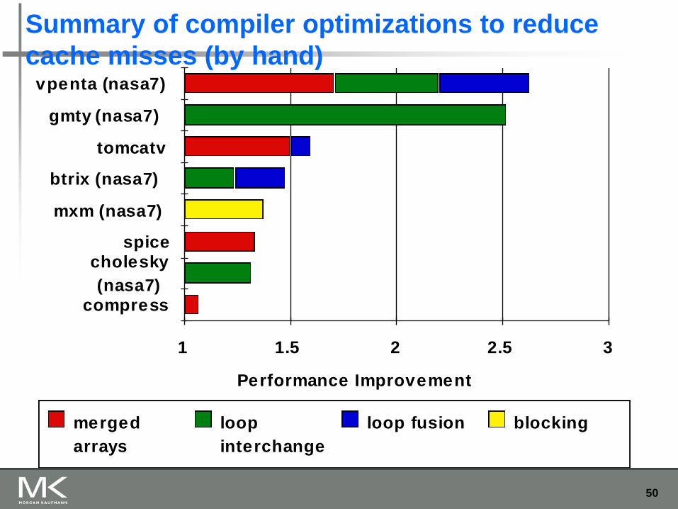
Performance Improvement
1 1.5 2 2.5 3
compress
cholesky
(nasa7)
spice
mxm (nasa7)
btrix (nasa7)
tomcatv
gmty (nasa7)
vpenta (nasa7)
merged
arrays
loop
interchange
loop fusion blocking
Summary of compiler optimizations to reduce
cache misses (by hand)
51
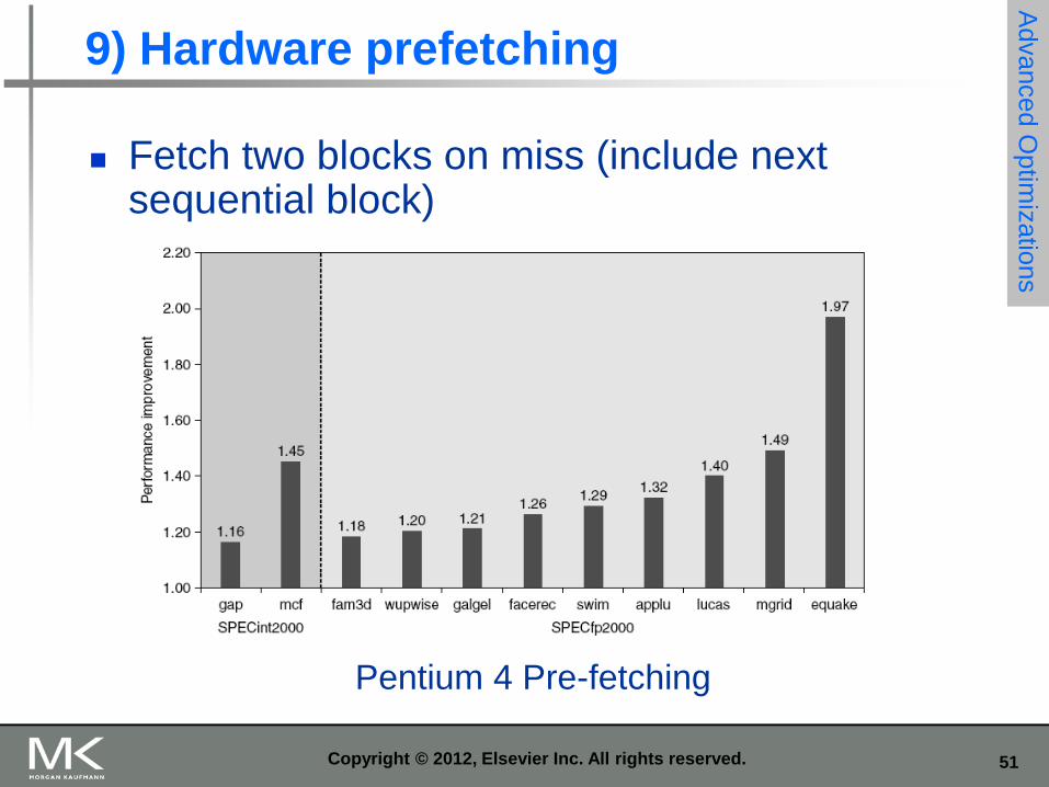
9) Hardware prefetching
Fetch two blocks on miss (include next sequential block)
Advanced O
ptim
izatio
ns
Pentium 4 Pre-fetching
Copyright © 2012, Elsevier Inc. All rights reserved.
52
10) Compiler prefetching
Insert prefetch instructions before data is needed
Non-faulting: prefetch doesn’t cause exceptions
Register prefetch Loads data into register
Cache prefetch Loads data into cache
Combine with loop unrolling and software pipelining
Advanced O
ptim
izatio
ns
Copyright © 2012, Elsevier Inc. All rights reserved.
53
Reducing misses by software prefetching
Data Prefetch Load data into register (HP PA-RISC loads)
Cache Prefetch: load into cache (MIPS IV, PowerPC, SPARC v. 9)
Special prefetching instructions cannot cause faults; a form of speculative execution
Issuing Prefetch Instructions takes time Is cost of prefetch issues < savings in reduced
misses?
Higher superscalar reduces difficulty of issue bandwidth
54
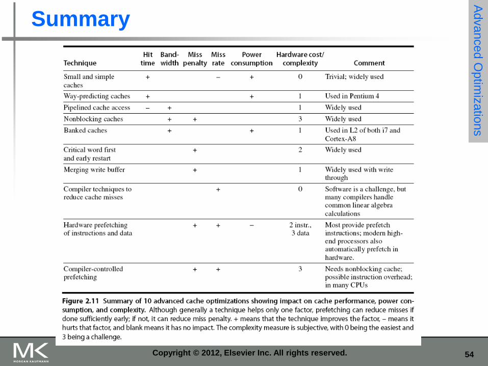
Summary A
dvanced O
ptim
izatio
ns
Copyright © 2012, Elsevier Inc. All rights reserved.
55
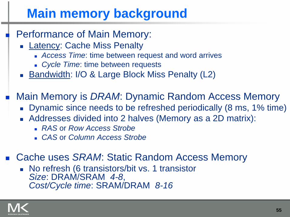
Main memory background
Performance of Main Memory: Latency: Cache Miss Penalty
Access Time: time between request and word arrives
Cycle Time: time between requests
Bandwidth: I/O & Large Block Miss Penalty (L2)
Main Memory is DRAM: Dynamic Random Access Memory Dynamic since needs to be refreshed periodically (8 ms, 1% time)
Addresses divided into 2 halves (Memory as a 2D matrix): RAS or Row Access Strobe
CAS or Column Access Strobe
Cache uses SRAM: Static Random Access Memory No refresh (6 transistors/bit vs. 1 transistor
Size: DRAM/SRAM 4-8, Cost/Cycle time: SRAM/DRAM 8-16
56
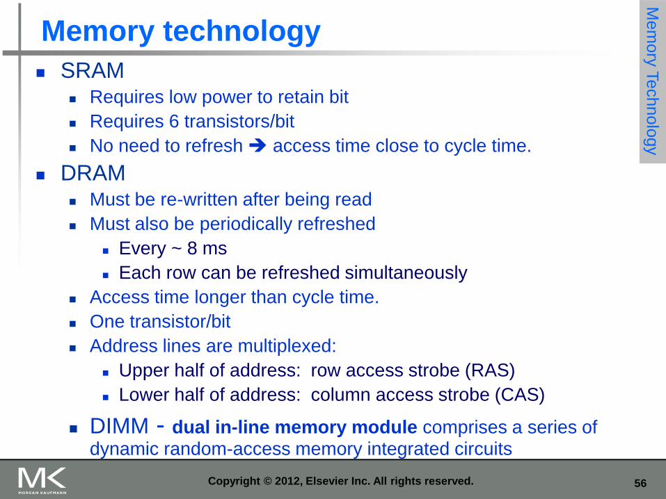
Memory technology
SRAM Requires low power to retain bit
Requires 6 transistors/bit
No need to refresh access time close to cycle time.
DRAM Must be re-written after being read
Must also be periodically refreshed
Every ~ 8 ms
Each row can be refreshed simultaneously
Access time longer than cycle time.
One transistor/bit
Address lines are multiplexed:
Upper half of address: row access strobe (RAS)
Lower half of address: column access strobe (CAS)
DIMM - dual in-line memory module comprises a series of dynamic random-access memory integrated circuits
Mem
ory
Technolo
gy
Copyright © 2012, Elsevier Inc. All rights reserved.
57
Memory technology
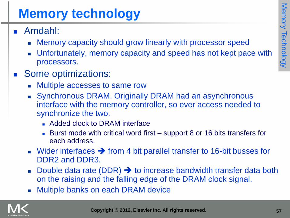
Amdahl: Memory capacity should grow linearly with processor speed
Unfortunately, memory capacity and speed has not kept pace with processors.
Some optimizations: Multiple accesses to same row
Synchronous DRAM. Originally DRAM had an asynchronous interface with the memory controller, so ever access needed to synchronize the two.
Added clock to DRAM interface
Burst mode with critical word first – support 8 or 16 bits transfers for each address.
Wider interfaces from 4 bit parallel transfer to 16-bit busses for DDR2 and DDR3.
Double data rate (DDR) to increase bandwidth transfer data both on the raising and the falling edge of the DRAM clock signal.
Multiple banks on each DRAM device
Mem
ory
Technolo
gy
Copyright © 2012, Elsevier Inc. All rights reserved.
58
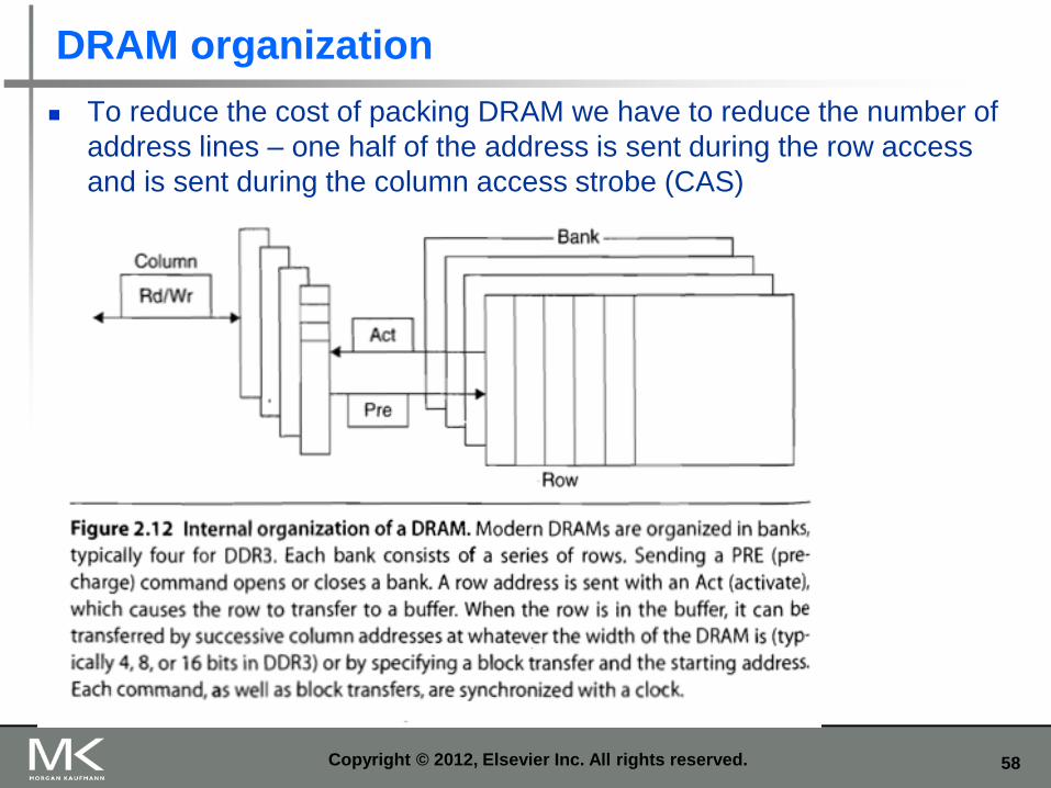
DRAM organization
To reduce the cost of packing DRAM we have to reduce the number of
address lines – one half of the address is sent during the row access
and is sent during the column access strobe (CAS)
Copyright © 2012, Elsevier Inc. All rights reserved.
59
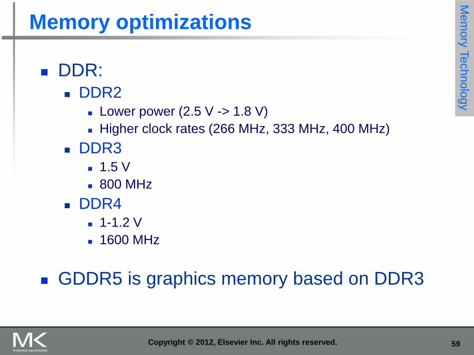
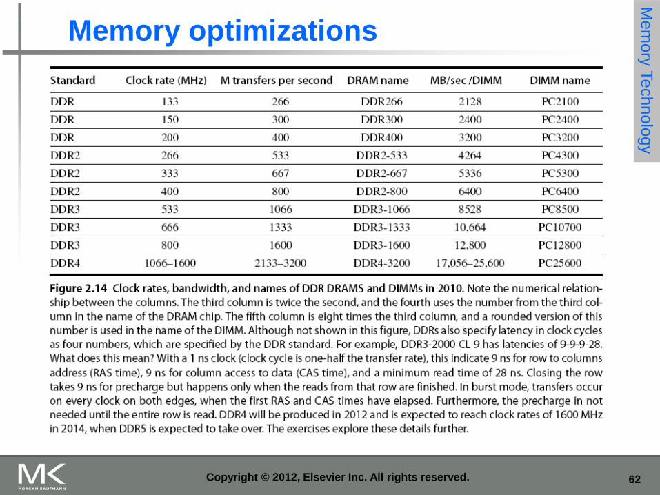
Memory optimizations
DDR: DDR2
Lower power (2.5 V -> 1.8 V)
Higher clock rates (266 MHz, 333 MHz, 400 MHz)
DDR3 1.5 V
800 MHz
DDR4 1-1.2 V
1600 MHz
GDDR5 is graphics memory based on DDR3
Mem
ory
Technolo
gy
Copyright © 2012, Elsevier Inc. All rights reserved.
60
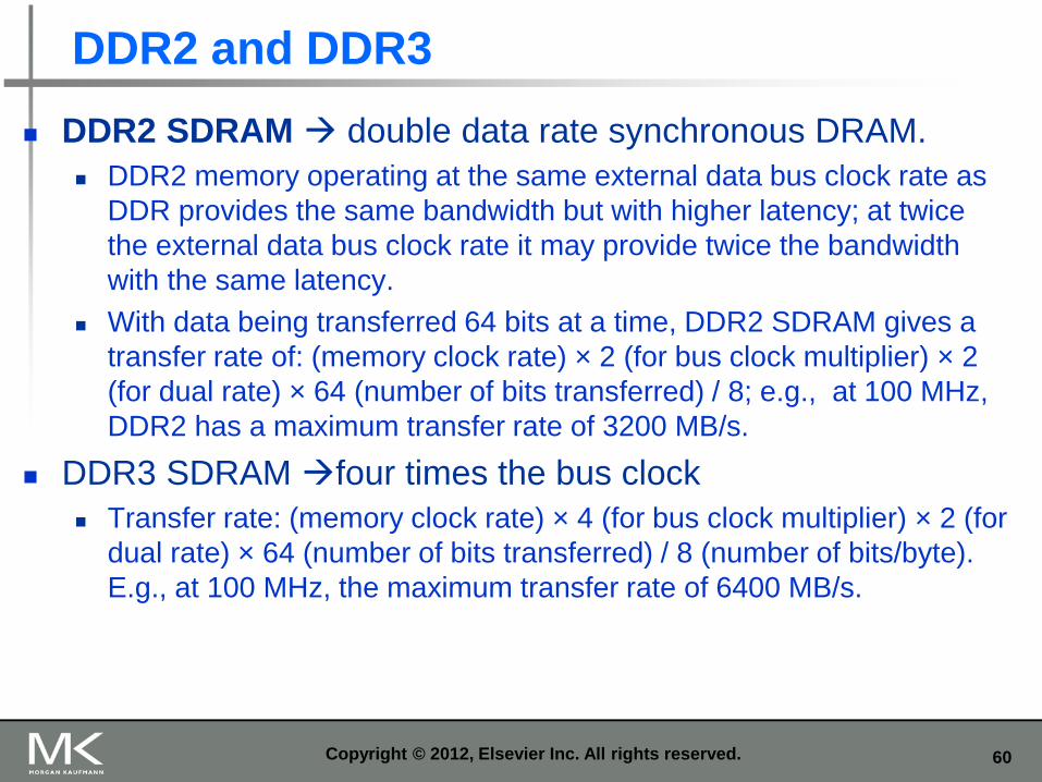
DDR2 and DDR3
DDR2 SDRAM double data rate synchronous DRAM.
DDR2 memory operating at the same external data bus clock rate as
DDR provides the same bandwidth but with higher latency; at twice
the external data bus clock rate it may provide twice the bandwidth
with the same latency.
With data being transferred 64 bits at a time, DDR2 SDRAM gives a
transfer rate of: (memory clock rate) × 2 (for bus clock multiplier) × 2
(for dual rate) × 64 (number of bits transferred) / 8; e.g., at 100 MHz,
DDR2 has a maximum transfer rate of 3200 MB/s.
DDR3 SDRAM four times the bus clock
Transfer rate: (memory clock rate) × 4 (for bus clock multiplier) × 2 (for
dual rate) × 64 (number of bits transferred) / 8 (number of bits/byte).
E.g., at 100 MHz, the maximum transfer rate of 6400 MB/s.
Copyright © 2012, Elsevier Inc. All rights reserved.
61
Memory optimizations M
em
ory
Technolo
gy
Copyright © 2012, Elsevier Inc. All rights reserved.
62 Copyright © 2012, Elsevier Inc. All rights reserved.
Memory optimizations M
em
ory
Technolo
gy
63
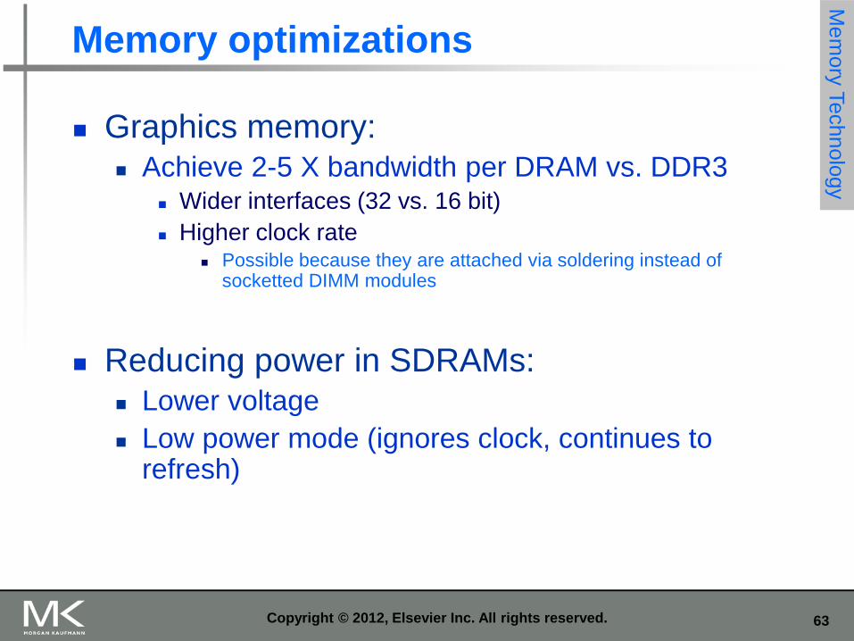
Memory optimizations
Graphics memory: Achieve 2-5 X bandwidth per DRAM vs. DDR3
Wider interfaces (32 vs. 16 bit)
Higher clock rate Possible because they are attached via soldering instead of
socketted DIMM modules
Reducing power in SDRAMs: Lower voltage
Low power mode (ignores clock, continues to refresh)
Mem
ory
Technolo
gy
Copyright © 2012, Elsevier Inc. All rights reserved.
64
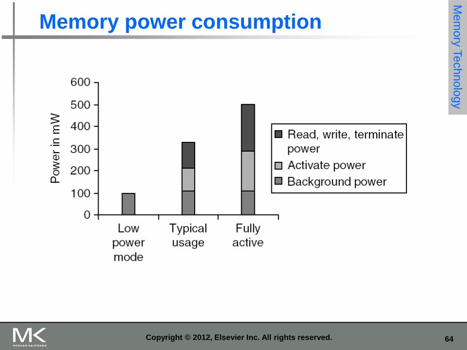
Memory power consumption M
em
ory
Technolo
gy
Copyright © 2012, Elsevier Inc. All rights reserved.
65
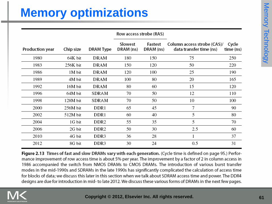
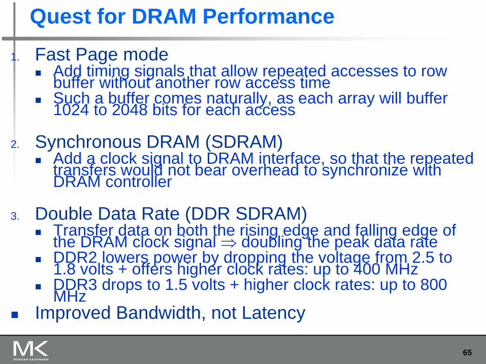
Quest for DRAM Performance
1. Fast Page mode Add timing signals that allow repeated accesses to row
buffer without another row access time Such a buffer comes naturally, as each array will buffer
1024 to 2048 bits for each access
2. Synchronous DRAM (SDRAM) Add a clock signal to DRAM interface, so that the repeated
transfers would not bear overhead to synchronize with DRAM controller
3. Double Data Rate (DDR SDRAM) Transfer data on both the rising edge and falling edge of
the DRAM clock signal doubling the peak data rate DDR2 lowers power by dropping the voltage from 2.5 to
1.8 volts + offers higher clock rates: up to 400 MHz DDR3 drops to 1.5 volts + higher clock rates: up to 800
MHz Improved Bandwidth, not Latency
66
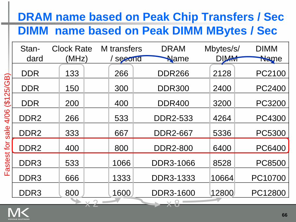
DRAM name based on Peak Chip Transfers / Sec
DIMM name based on Peak DIMM MBytes / Sec
Stan-
dard
Clock Rate
(MHz)
M transfers
/ second
DRAM
Name
Mbytes/s/
DIMM
DIMM
Name
DDR 133 266 DDR266 2128 PC2100
DDR 150 300 DDR300 2400 PC2400
DDR 200 400 DDR400 3200 PC3200
DDR2 266 533 DDR2-533 4264 PC4300
DDR2 333 667 DDR2-667 5336 PC5300
DDR2 400 800 DDR2-800 6400 PC6400
DDR3 533 1066 DDR3-1066 8528 PC8500
DDR3 666 1333 DDR3-1333 10664 PC10700
DDR3 800 1600 DDR3-1600 12800 PC12800
x 2 x 8
Faste
st fo
r sale
4/0
6 (
$125/G
B)
67
The need for error correction!
Motivation: Failures/time proportional to number of bits! As DRAM cells shrink, more vulnerable
Went through period in which failure rate was low enough without error correction that people didn’t do correction DRAM banks too large now Servers always corrected memory systems
Basic idea: add redundancy through parity bits Common configuration: Random error correction
SEC-DED (single error correct, double error detect) One example: 64 data bits + 8 parity bits (11% overhead)
Really want to handle failures of physical components as well Organization is multiple DRAMs/DIMM, multiple DIMMs Want to recover from failed DRAM and failed DIMM! “Chip kill” handle failures width of single DRAM chip
68
AMD Opteron memory hierarchy
12-stage integer pipeline yields a maximum clock rate of 2.8 GHz
and fastest memory PC3200 DDR SDRAM
48-bit virtual and 40-bit physical addresses
I and D cache: 64 KB, 2-way set associative, 64-B block, LRU
L2 cache: 1 MB, 16-way, 64-B block, pseudo LRU
Data and L2 caches use write back, write allocate
L1 caches are virtually indexed and physically tagged
L1 I TLB and L1 D TLB: fully associative, 40 entries
32 entries for 4 KB pages and 8 for 2 MB or 4 MB pages
L2 I TLB and L1 D TLB: 4-way, 512 entities of 4 KB pages
Memory controller allows up to 10 cache misses
8 from D cache and 2 from I cache
69
Opteron memory hierarchy performance
For SPEC2000
I cache misses per instruction is 0.01% to 0.09%
D cache misses per instruction are 1.34% to 1.43%
L2 cache misses per instruction are 0.23% to 0.36%
Commercial benchmark (“TPC-C-like”)
I cache misses per instruction is 1.83% (100X!)
D cache misses per instruction are 1.39% ( same)
L2 cache misses per instruction are 0.62% (2X to 3X)
How does it compare to ideal CPI of 0.33?
70
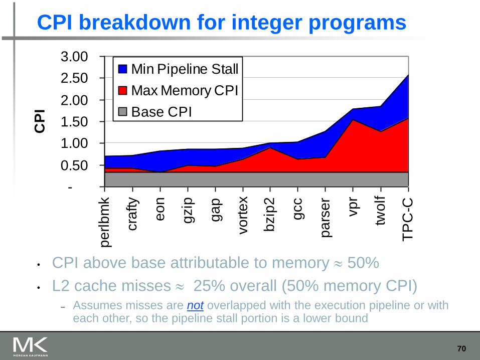
CPI breakdown for integer programs
-
0.50
1.00
1.50
2.00
2.50
3.00
pe
rlb
mk
cra
fty
eo
n
gzip
ga
p
vo
rte
x
bzip
2
gcc
pa
rse
r
vp
r
two
lf
TP
C-C
CP
I
Min Pipeline Stall
Max Memory CPI
Base CPI
• CPI above base attributable to memory 50%
• L2 cache misses 25% overall (50% memory CPI) – Assumes misses are not overlapped with the execution pipeline or with
each other, so the pipeline stall portion is a lower bound
71
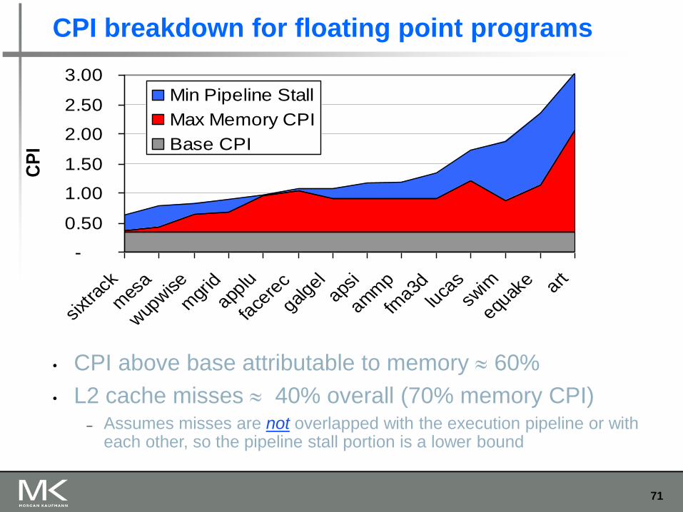
CPI breakdown for floating point programs
• CPI above base attributable to memory 60%
• L2 cache misses 40% overall (70% memory CPI) – Assumes misses are not overlapped with the execution pipeline or with
each other, so the pipeline stall portion is a lower bound
-
0.50
1.00
1.50
2.00
2.50
3.00
sixt
rack
mes
a
wup
wise
mgr
id
applu
face
rec
galgel
apsi
amm
p
fma3d
luca
s
swim
equak
e art
CP
I
Min Pipeline Stall
Max Memory CPI
Base CPI
72
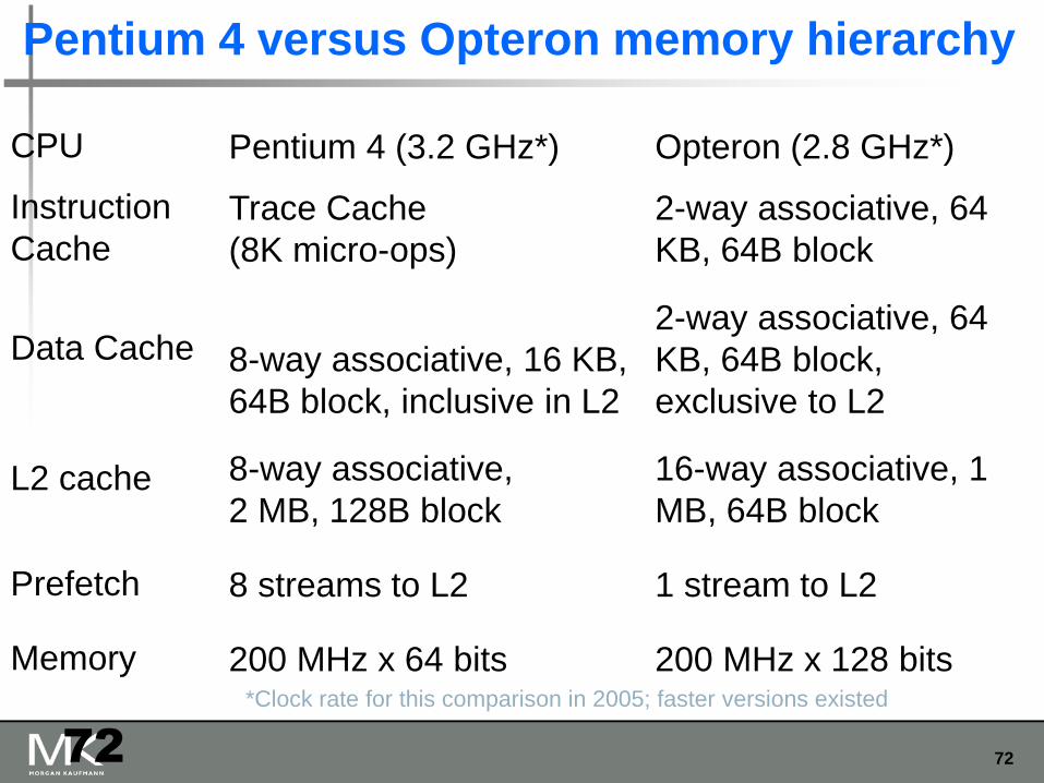
Pentium 4 versus Opteron memory hierarchy
CPU Pentium 4 (3.2 GHz*) Opteron (2.8 GHz*)
Instruction
Cache
Trace Cache
(8K micro-ops)
2-way associative, 64
KB, 64B block
Data Cache 8-way associative, 16 KB,
64B block, inclusive in L2
2-way associative, 64
KB, 64B block,
exclusive to L2
L2 cache 8-way associative,
2 MB, 128B block
16-way associative, 1
MB, 64B block
Prefetch 8 streams to L2 1 stream to L2
Memory 200 MHz x 64 bits 200 MHz x 128 bits *Clock rate for this comparison in 2005; faster versions existed
72
73
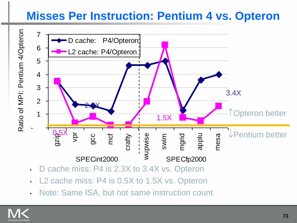
Misses Per Instruction: Pentium 4 vs. Opteron
-
1
2
3
4
5
6
7
gzip vpr
gcc
mcf
cra
fty
wu
pw
ise
sw
im
mgrid
ap
plu
mesa
Ratio o
f M
PI:
Pentium
4/O
pte
ron
D cache: P4/Opteron
L2 cache: P4/Opteron
SPECint2000 SPECfp2000
Opteron better
Pentium better
• D cache miss: P4 is 2.3X to 3.4X vs. Opteron
• L2 cache miss: P4 is 0.5X to 1.5X vs. Opteron
• Note: Same ISA, but not same instruction count
2.3X
3.4X
0.5X
1.5X
74
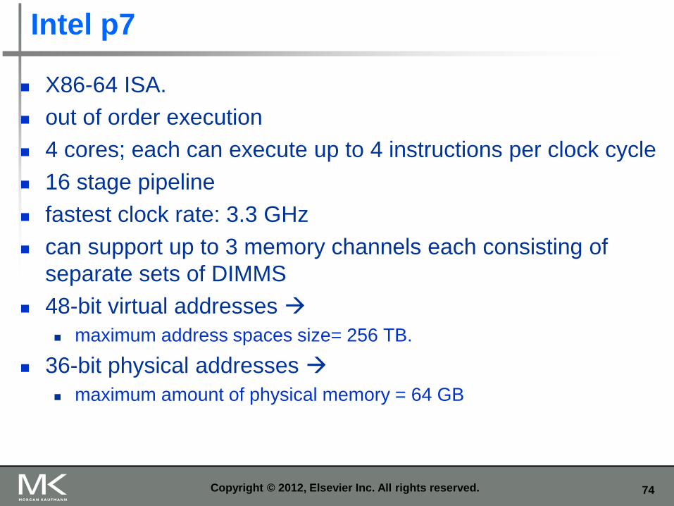
Intel p7
X86-64 ISA.
out of order execution
4 cores; each can execute up to 4 instructions per clock cycle
16 stage pipeline
fastest clock rate: 3.3 GHz
can support up to 3 memory channels each consisting of
separate sets of DIMMS
48-bit virtual addresses
maximum address spaces size= 256 TB.
36-bit physical addresses
maximum amount of physical memory = 64 GB
Copyright © 2012, Elsevier Inc. All rights reserved.
75
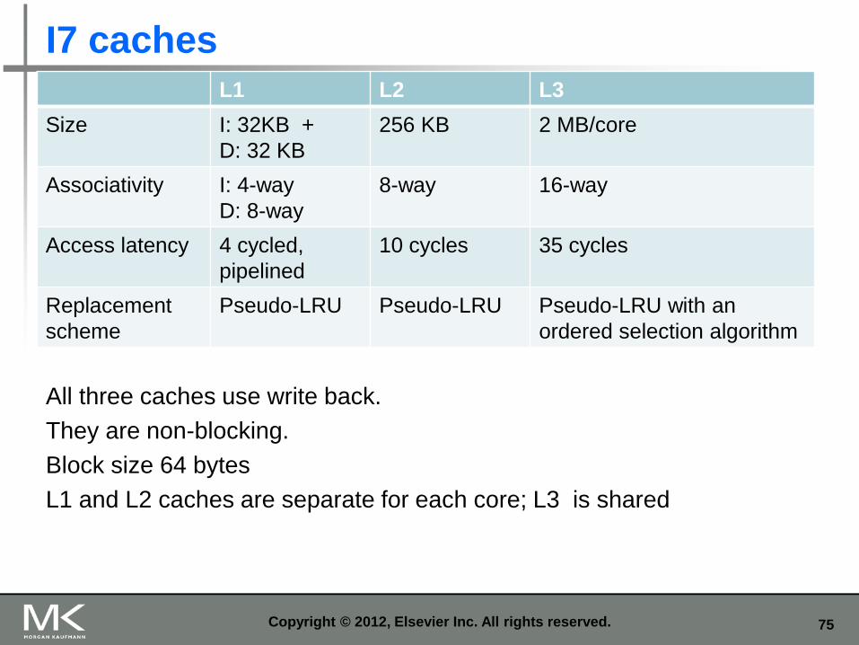
I7 caches L1 L2 L3
Size I: 32KB +
D: 32 KB
256 KB 2 MB/core
Associativity I: 4-way
D: 8-way
8-way 16-way
Access latency 4 cycled,
pipelined
10 cycles 35 cycles
Replacement
scheme
Pseudo-LRU Pseudo-LRU Pseudo-LRU with an
ordered selection algorithm
Copyright © 2012, Elsevier Inc. All rights reserved.
All three caches use write back.
They are non-blocking.
Block size 64 bytes
L1 and L2 caches are separate for each core; L3 is shared
76
Flash memory
Type of EEPROM
Must be erased (in blocks) before being overwritten
Non volatile
Limited number of write cycles
Cheaper than SDRAM, more expensive than disk
Slower than SRAM, faster than disk
Mem
ory
Technolo
gy
Copyright © 2012, Elsevier Inc. All rights reserved.
77
Memory dependability
Memory is susceptible to cosmic rays
Soft errors: dynamic errors Detected and fixed by error correcting codes
(ECC)
Hard errors: permanent errors Use sparse rows to replace defective rows
Chipkill: a RAID-like error recovery technique
Mem
ory
Technolo
gy
Copyright © 2012, Elsevier Inc. All rights reserved.
78
Virtual memory
Each process has its own address space. In a 32-bit architecture each process can address up to 232 bytes (4 GB); in a 64–bit architecture a process can address up to 264 bytes.
Protection via virtual memory
Keeps processes in their own memory space
The role of architecture:
Provide user mode and supervisor mode
Protect certain aspects of CPU state
Provide mechanisms for switching between user mode and supervisor mode
Provide mechanisms to limit memory accesses
Provide TLB to translate addresses
Virtu
al M
em
ory
and V
irtual M
achin
es
Copyright © 2012, Elsevier Inc. All rights reserved.
79
Dynamic address translation
Virtual address address generated by compiler
Physical address address in physical memory
Dynamic address translation mapping a virtual address to a physical
address.
Virtual memory organization: paging and segmentation.
Page a set of consecutive virtual addresses.
Page size typically 2 – 4 KB
All pages of a process are stored on the secondary storage (disk) in a
region called “swap area.” The size of “swap area” on the disk= the
address space size X the max number of processes.
Each process has its own “page table.” A page table entry shows
The “page frame” in physical memory where the page resides if the
“valid bit” is ON.
The need to bring in the page if the “valid bit” is OFF and then a “page
fault” occurs, the page must be brought in from the secondary
storage.
Copyright © 2012, Elsevier Inc. All rights reserved.
80
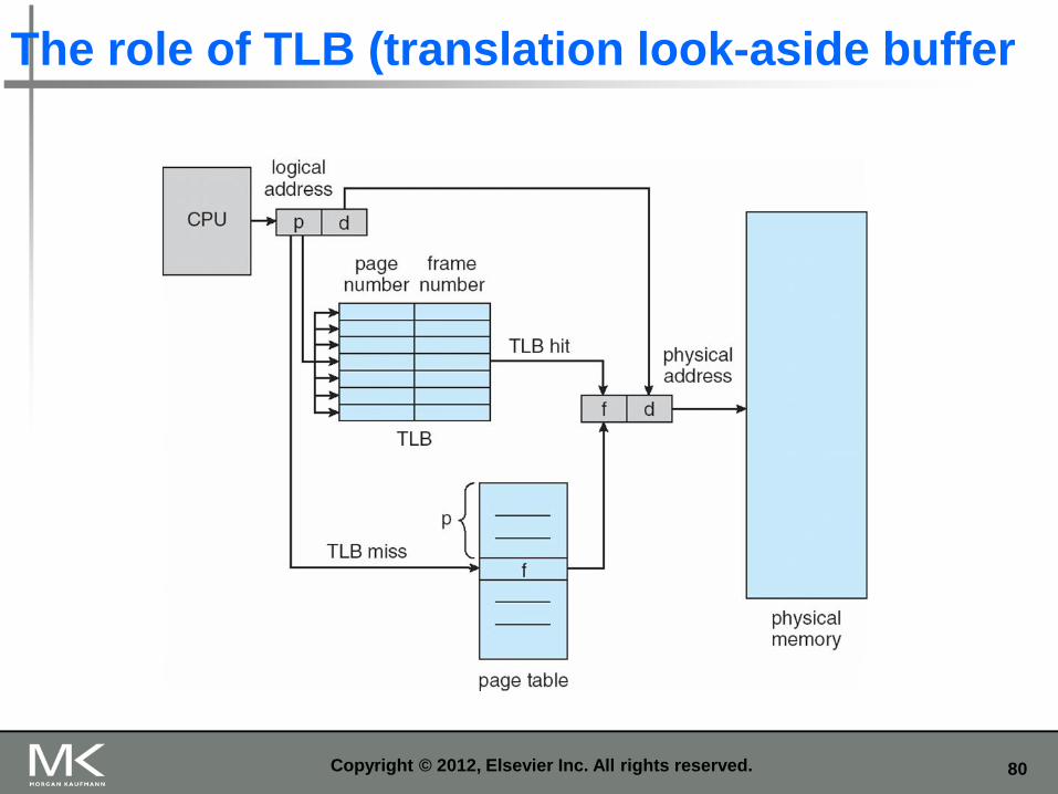
The role of TLB (translation look-aside buffer
Copyright © 2012, Elsevier Inc. All rights reserved.
81
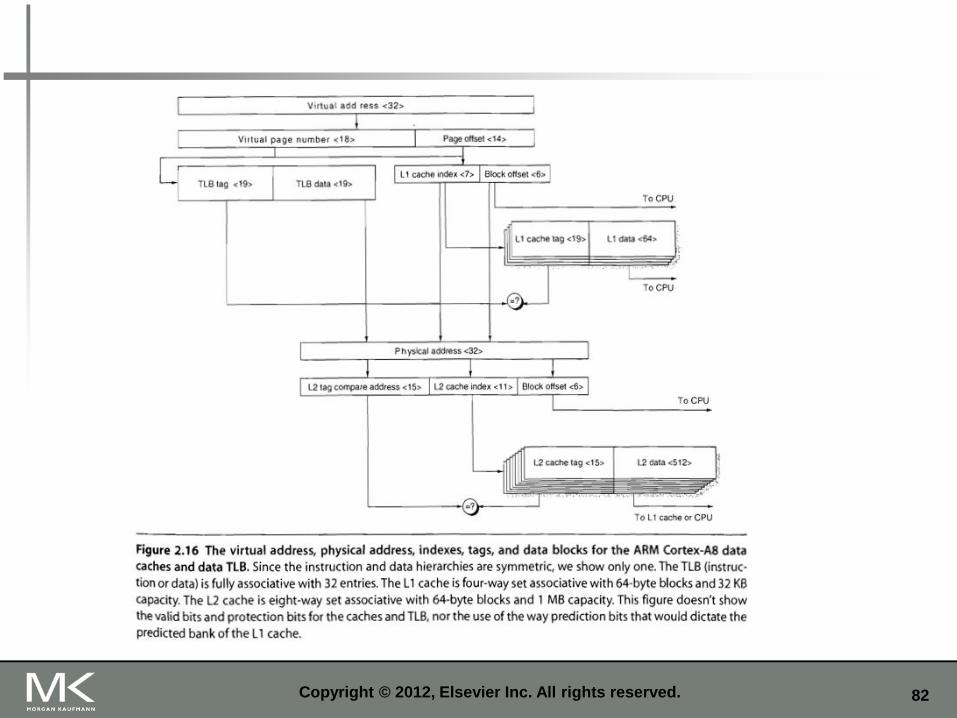
The ARM Cortex A8
Supports ARMv7 instruction set.
Can issue two instructions per clock cycle; clock cycle up to 1 GHz.
Two-level cache hierarchy
A pair of L1- instruction (I) and data (D).
Each has Capacity =32 KB with block size=64 byte
Four-way set associative
Virtually indexed and physically tagged
L2 cache.
Capacity= 1 MB;
Bloc size = 64 byte;
Eight=way set associative.
Physically indexed and tagged.
Copyright © 2012, Elsevier Inc. All rights reserved.
82 Copyright © 2012, Elsevier Inc. All rights reserved.
83 Copyright © 2012, Elsevier Inc. All rights reserved.
84
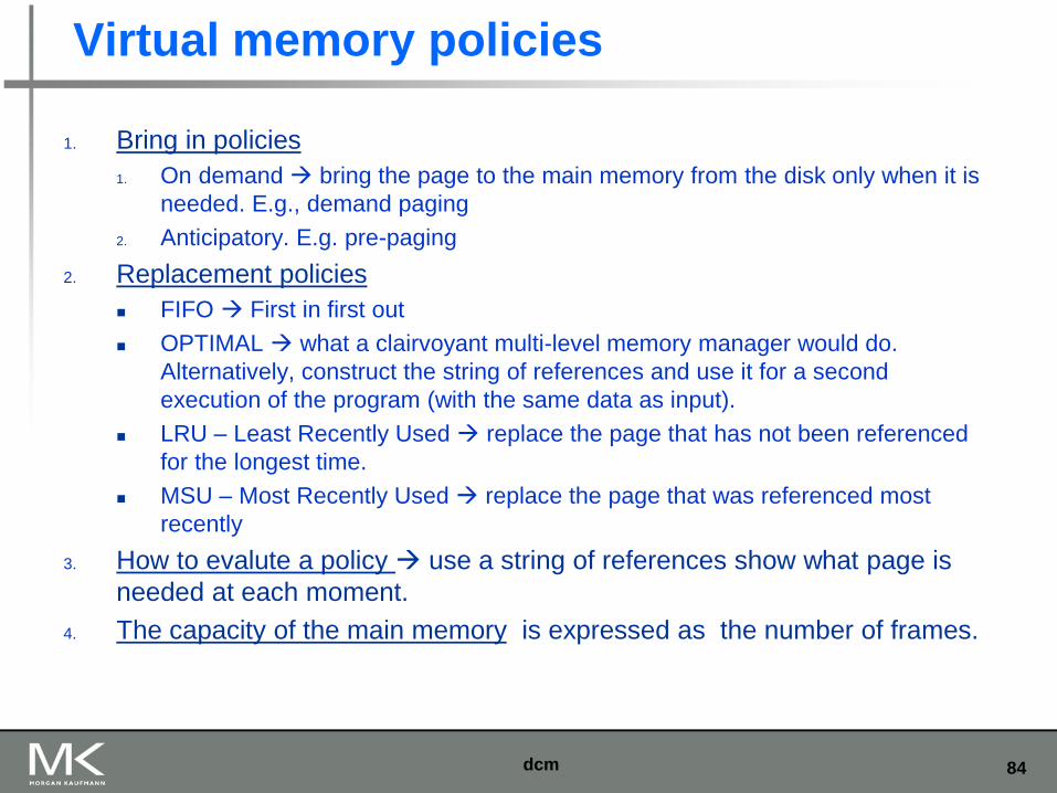
Virtual memory policies
1. Bring in policies
1. On demand bring the page to the main memory from the disk only when it is
needed. E.g., demand paging
2. Anticipatory. E.g. pre-paging
2. Replacement policies
FIFO First in first out
OPTIMAL what a clairvoyant multi-level memory manager would do.
Alternatively, construct the string of references and use it for a second
execution of the program (with the same data as input).
LRU – Least Recently Used replace the page that has not been referenced
for the longest time.
MSU – Most Recently Used replace the page that was referenced most
recently
3. How to evalute a policy use a string of references show what page is
needed at each moment.
4. The capacity of the main memory is expressed as the number of frames.
dcm
85
Page replacement policies; Belady’s anomaly
In the following examples we use a given string of references to illustrate
several page replacement policies. We have five pages, 0, 1, 2, 3, and 4.
The main memory has a capacity of
3 frames, labeled 0,1,2
4 frames, labeled 0, 1, 2, 3
Once a frame has the “dirty bit” on it means that the page residing in that
frame was modifies and must be written back to the secondary device, the
disk before being replaced.
The capacity of the primary device is important. One expects that increasing
the capacity, in our case the number of frames in RAM leads to a higher hit
ratio. That is not always the case as our examples will show. This is the
Belady’s anomaly.
Note: different results are obtained with a different string of references!!
dcm
86
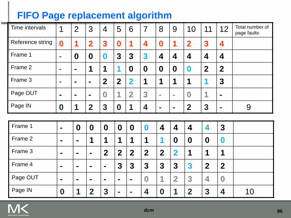
Time intervals 1 2 3 4 5 6 7 8 9 10 11 12 Total number of
page faults
Reference string 0 1 2 3 0 1 4 0 1 2 3 4
Frame 1 - 0 0 0 3 3 3 4 4 4 4 4
Frame 2 - - 1 1 1 0 0 0 0 0 2 2
Frame 3 - - - 2 2 2 1 1 1 1 1 3
Page OUT - - - 0 1 2 3 - - 0 1 -
Page IN 0 1 2 3 0 1 4 - - 2 3 - 9
Frame 1 - 0 0 0 0 0 0 4 4 4 4 3
Frame 2 - - 1 1 1 1 1 1 0 0 0 0
Frame 3 - - - 2 2 2 2 2 2 1 1 1
Frame 4 - - - - 3 3 3 3 3 3 2 2
Page OUT - - - - - - 0 1 2 3 4 0
Page IN 0 1 2 3 - - 4 0 1 2 3 4 10
FIFO Page replacement algorithm
dcm
87
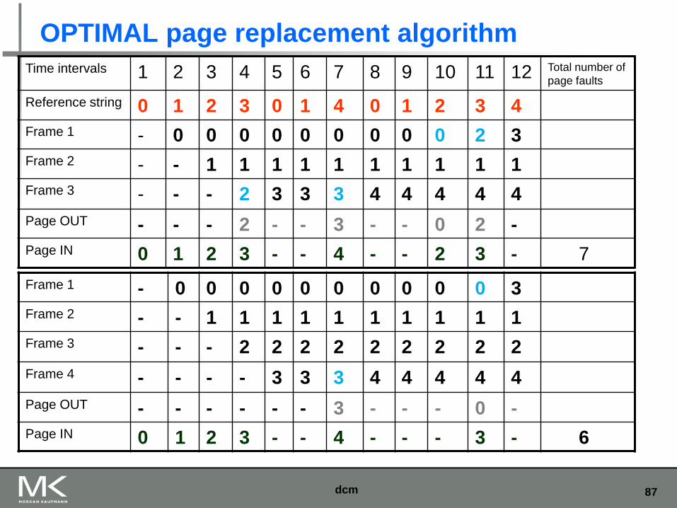
Time intervals 1 2 3 4 5 6 7 8 9 10 11 12 Total number of
page faults
Reference string 0 1 2 3 0 1 4 0 1 2 3 4
Frame 1 - 0 0 0 0 0 0 0 0 0 2 3
Frame 2 - - 1 1 1 1 1 1 1 1 1 1
Frame 3 - - - 2 3 3 3 4 4 4 4 4
Page OUT - - - 2 - - 3 - - 0 2 -
Page IN 0 1 2 3 - - 4 - - 2 3 - 7
Frame 1 - 0 0 0 0 0 0 0 0 0 0 3
Frame 2 - - 1 1 1 1 1 1 1 1 1 1
Frame 3 - - - 2 2 2 2 2 2 2 2 2
Frame 4 - - - - 3 3 3 4 4 4 4 4
Page OUT - - - - - - 3 - - - 0 -
Page IN 0 1 2 3 - - 4 - - - 3 - 6
OPTIMAL page replacement algorithm
dcm
88
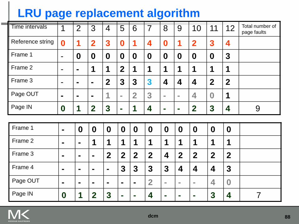
Time intervals 1 2 3 4 5 6 7 8 9 10 11 12 Total number of
page faults
Reference string 0 1 2 3 0 1 4 0 1 2 3 4
Frame 1 - 0 0 0 0 0 0 0 0 0 0 3
Frame 2 - - 1 1 2 1 1 1 1 1 1 1
Frame 3 - - - 2 3 3 3 4 4 4 2 2
Page OUT - - - 1 - 2 3 - - 4 0 1
Page IN 0 1 2 3 - 1 4 - - 2 3 4 9
Frame 1 - 0 0 0 0 0 0 0 0 0 0 0
Frame 2 - - 1 1 1 1 1 1 1 1 1 1
Frame 3 - - - 2 2 2 2 4 2 2 2 2
Frame 4 - - - - 3 3 3 3 4 4 4 3
Page OUT - - - - - - 2 - - - 4 0
Page IN 0 1 2 3 - - 4 - - - 3 4 7
LRU page replacement algorithm
dcm
89
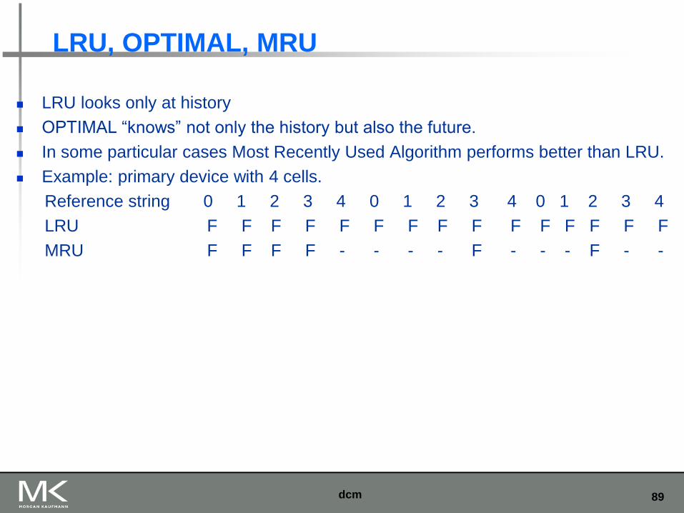
LRU, OPTIMAL, MRU
LRU looks only at history
OPTIMAL “knows” not only the history but also the future.
In some particular cases Most Recently Used Algorithm performs better than LRU.
Example: primary device with 4 cells.
Reference string 0 1 2 3 4 0 1 2 3 4 0 1 2 3 4
LRU F F F F F F F F F F F F F F F
MRU F F F F - - - - F - - - F - -
dcm
90
Time intervals 1 2 3 4 5 6 7 8 9 10 11 12 Total number of
page faults
Reference string 0 1 2 3 0 1 4 0 1 2 3 4
Frame 1 - 0 0 0 0 0 0 0 0 0 2 3
Frame 2 - - 1 1 1 1 1 1 1 1 1 1
Frame 3 - - - 2 3 3 3 4 4 4 4 4
Page OUT - - - 2 - - 3 - - 0 2 -
Page IN 0 1 2 3 - - 4 - - 2 3 - 7
Frame 1 - 0 0 0 0 0 0 0 0 0 0 3
Frame 2 - - 1 1 1 1 1 1 1 1 1 1
Frame 3 - - - 2 2 2 2 2 2 2 2 2
Frame 4 - - - - 3 3 3 4 4 4 4 4
Page OUT - - - - - - 3 - - - 0 -
Page IN 0 1 2 3 - - 4 - - - 3 - 6
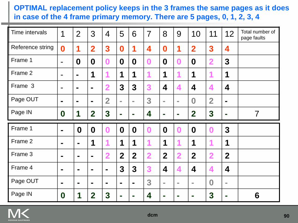
OPTIMAL replacement policy keeps in the 3 frames the same pages as it does
in case of the 4 frame primary memory. There are 5 pages, 0, 1, 2, 3, 4
dcm
91
Time intervals 1 2 3 4 5 6 7 8 9 10 11 12 Total number of
page faults
Reference string 0 1 2 3 0 1 4 0 1 2 3 4
Frame 1 - 0 0 0 0 0 0 0 0 0 0 3
Frame 2 - - 1 1 2 1 1 1 1 1 1 1
Frame 3 - - - 2 3 3 3 4 4 4 2 2
Page OUT - - - 2 - - 3 - - 0 2 -
Page IN 0 1 2 3 - 1 4 - - 2 3 4 9
Frame 1 - 0 0 0 0 0 0 0 0 0 0 0
Frame 2 - - 1 1 1 1 1 1 1 1 1 1
Frame 3 - - - 2 2 2 2 4 2 2 2 2
Frame 4 - - - - 3 3 3 3 4 4 4 3
Page OUT - - - - - - 2 - - - 4 0
Page IN 0 1 2 3 - - 4 - - - 3 4 7
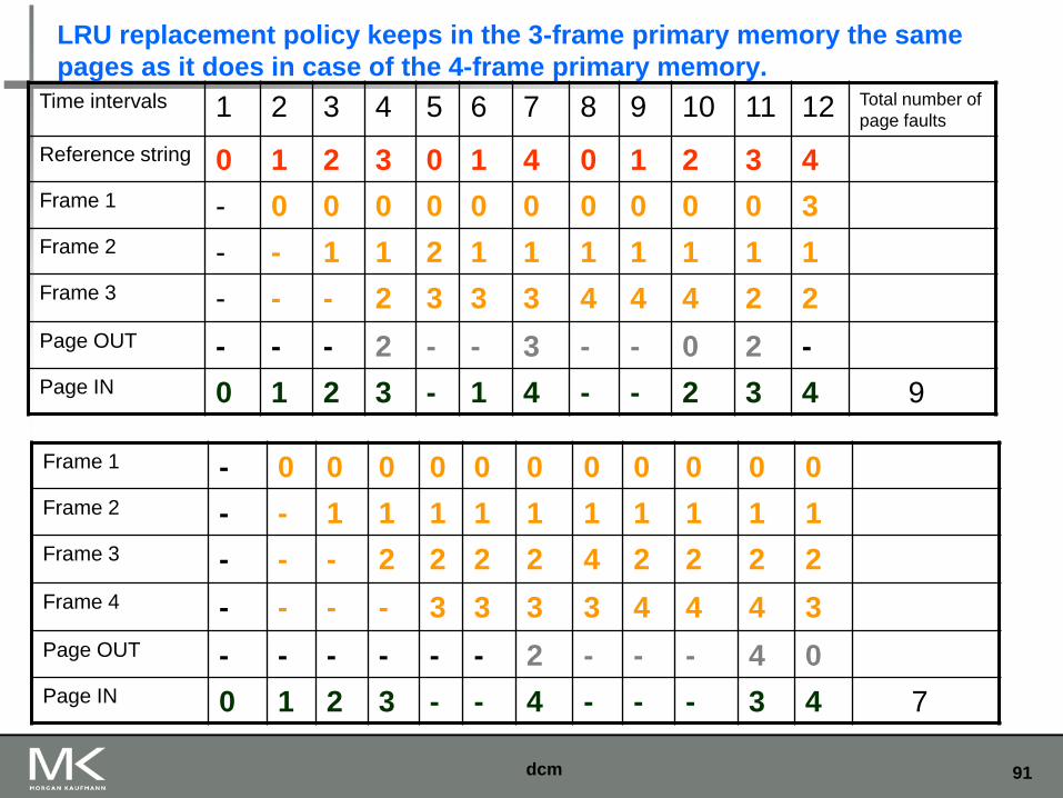
LRU replacement policy keeps in the 3-frame primary memory the same
pages as it does in case of the 4-frame primary memory.
dcm
92
Time intervals 1 2 3 4 5 6 7 8 9 10 11 12 Total number of
page faults
Reference string 0 1 2 3 0 1 4 0 1 2 3 4
Frame 1 - 0 0 0 3 3 3 4 4 4 4 4
Frame 2 - - 1 1 1 0 0 0 0 0 2 2
Frame 3 - - - 2 2 2 1 1 1 1 1 3
Page OUT - - - 0 1 2 3 - - 0 1 -
Page IN 0 1 2 3 0 1 4 - - 2 3 - 9
Frame 1 - 0 0 0 0 0 0 4 4 4 4 3
Frame 2 - - 1 1 1 1 1 1 0 0 0 0
Frame 3 - - - 2 2 2 2 2 2 1 1 1
Frame 4 - - - - 3 3 3 3 3 3 2 2
Page OUT - - - - - - 0 1 2 3 4 0
Page IN 0 1 2 3 - - 4 0 1 2 3 4 10
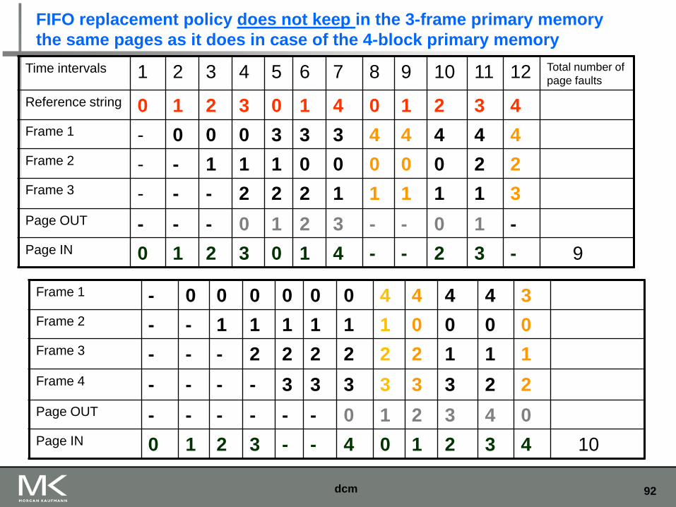
FIFO replacement policy does not keep in the 3-frame primary memory
the same pages as it does in case of the 4-block primary memory
dcm
93
How to avoid Belady’s anomaly
The OPTIMAL and the LRU algorithms have the subset property, a primary
device with a smaller capacity hold a subset of the pages a primary device
with a larger capacity could hold.
The subset property creates a total ordering. If the primary system has 1
blocks and contains page A a system with two block add page B, and a
system with three blocks will add page C. Thus we have a total ordering
AB C or (A,B,C)
Replacement algorithms that have the subset property are called “stack”
algorithms.
If we use stack replacement algorithms a device with a larger capacity can
never have more page faults than the one with a smaller capacity.
m the pages held by a primary device with smaller capacity
n the pages held by a primary device with larger capacity
m is a subset of n
dcm
94
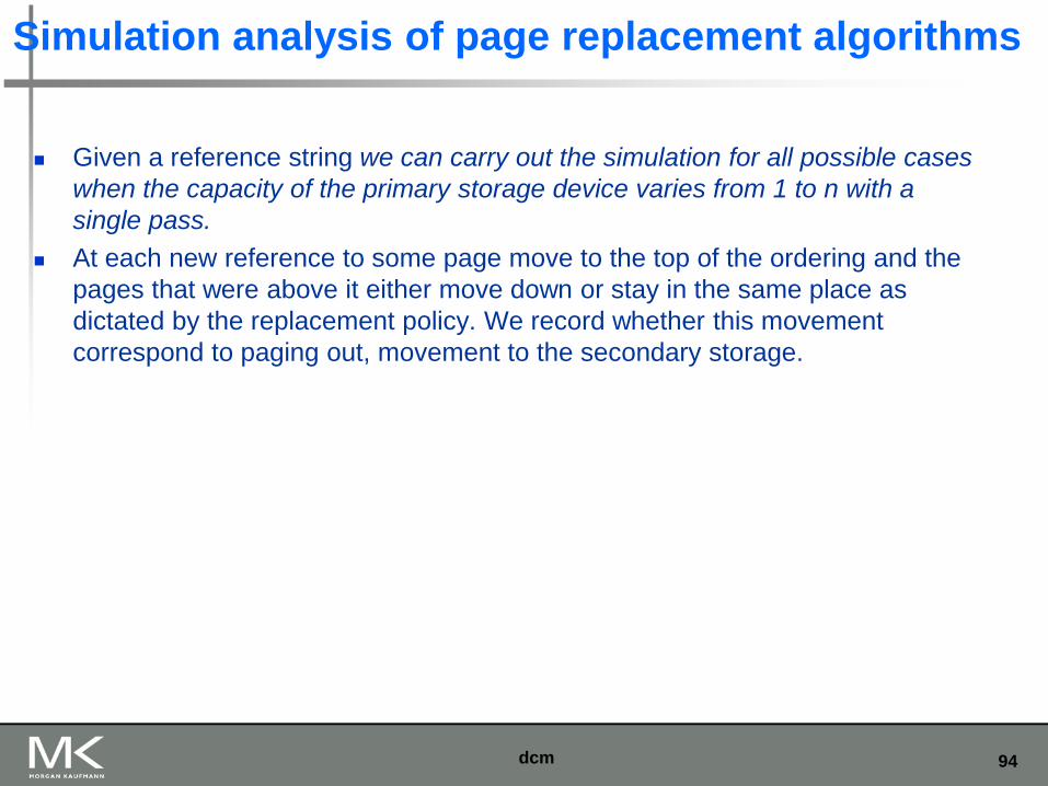
Simulation analysis of page replacement algorithms
Given a reference string we can carry out the simulation for all possible cases
when the capacity of the primary storage device varies from 1 to n with a
single pass.
At each new reference to some page move to the top of the ordering and the
pages that were above it either move down or stay in the same place as
dictated by the replacement policy. We record whether this movement
correspond to paging out, movement to the secondary storage.
dcm
95
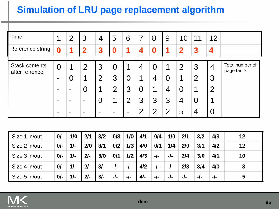
Time 1 2 3 4 5 6 7 8 9 10 11 12
Reference string 0 1 2 3 0 1 4 0 1 2 3 4
Size 1 in/out 0/- 1/0 2/1 3/2 0/3 1/0 4/1 0/4 1/0 2/1 3/2 4/3 12
Size 2 in/out 0/- 1/- 2/0 3/1 0/2 1/3 4/0 0/1 1/4 2/0 3/1 4/2 12
Size 3 in/out 0/- 1/- 2/- 3/0 0/1 1/2 4/3 -/- -/- 2/4 3/0 4/1 10
Size 4 in/out 0/- 1/- 2/- 3/- -/- -/- 4/2 -/- -/- 2/3 3/4 4/0 8
Size 5 in/out 0/- 1/- 2/- 3/- -/- -/- 4/- -/- -/- -/- -/- -/- 5
Simulation of LRU page replacement algorithm
Stack contents
after refrence 0
-
-
-
-
1
0
-
-
-
2
1
0
-
-
3
2
1
0
-
0
3
2
1
-
1
0
3
2
-
4
1
0
3
2
0
4
1
3
2
1
0
4
3
2
2
1
0
4
5
3
2
1
0
4
4
3
2
1
0
Total number of
page faults
dcm
96
Time 1 2 3 4 5 6 7 8 9 10 11 12
Reference string 0 1 2 3 0 1 4 0 1 2 3 4
Size 1 victim - 0 1 2 3 0 1 4 0 1 2 3 11
Size 2 victim - - 1 2 - 3 1 - 1 2 3 4 10
Size 3 victim - - - 2 - - 4 - - 2 3 - 7
Size 4 victim - - - - - - 4 - - 2 - - 6
Size 5 victim - - - - - - - - - - - - 5
Simulation of OPTIMUM
Stack contents
after reference 0
-
-
-
-
1
0
-
-
-
2
0
1
-
-
3
0
1
2
-
0
3
1
2
-
1
0
3
2
-
4
0
1
3
2
0
4
1
3
2
1
0
4
3
2
2
0
4
3
1
3
0
4
2
1
4
0
3
2
1
Total number
of page faults
dcm
97
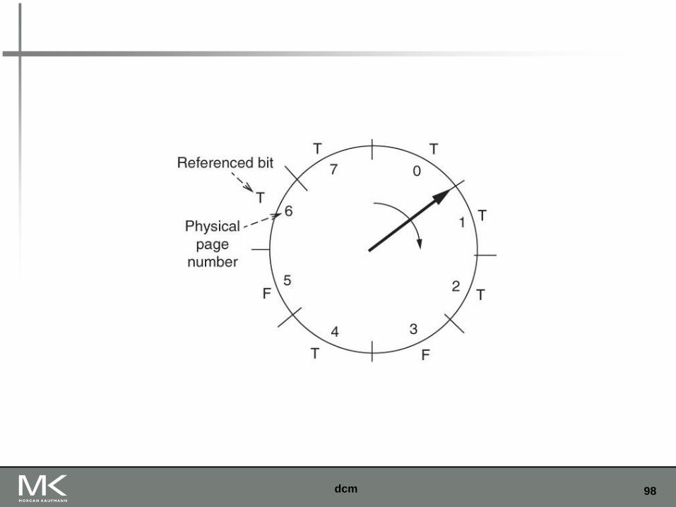
Clock replacement algorithm
Approximates LRU with a minimum
Additional hardware: one reference bit for each page
Overhead
Algorithm activated :
when a new page must be brought in move the pointer of a virtual clock
in clockwise direction
if the arm points to a block with reference bit TRUE
Set it FALSE
Move to the next block
if the arm points to a block with reference bit FALSE
The page in that block could be removed (has not been referenced for a
while)
Write it back to the secondary storage if the “dirty” bit is on (if the page has
been modified.
dcm
98 dcm
99
Virtual machines
Supports isolation and security
Sharing a computer among many unrelated users
Enabled by raw speed of processors, making the overhead more acceptable
Allows different ISAs and operating systems to be presented to user programs “System Virtual Machines”
SVM software is called “virtual machine monitor” or “hypervisor”
Individual virtual machines run under the monitor are called “guest VMs”
Virtu
al M
em
ory
and V
irtual M
achin
es
Copyright © 2012, Elsevier Inc. All rights reserved.
100
Impact of VMs on virtual memory
Each guest OS maintains its own set of page tables VMM adds a level of memory between physical
and virtual memory called “real memory”
VMM maintains shadow page table that maps guest virtual addresses to physical addresses Requires VMM to detect guest’s changes to its own page
table
Occurs naturally if accessing the page table pointer is a privileged operation
Virtu
al M
em
ory
and V
irtual M
achin
es
Copyright © 2012, Elsevier Inc. All rights reserved.