buck converter design - mouser electronics deutschland · buck converter design 2 design note dn...
TRANSCRIPT

Design Note DN 2013-01
V1.0 January 2013
Buck Converter Design
Jens Ejury
Infineon Technologies North America (IFNA) Corp.

Buck Converter Design
2
Design Note DN 2013-01
V0.1 January 2013
Published by Infineon Technologies North America 27703 Emperor Blvd, suite 310 Durham, NC 27703 All Rights Reserved.
Attention please!
THE INFORMATION GIVEN IN THIS APPLICATION NOTE IS GIVEN AS A HINT FOR THE IMPLEMEN-TATION OF THE INFINEON TECHNOLOGIES COMPONENT ONLY AND SHALL NOT BE REGARDED AS ANY DESCRIPTION OR WARRANTY OF A CERTAIN FUNCTIONALITY, CONDITION OR QUALITY OF THE INFINEON TECHNOLOGIES COMPONENT. THE RECIPIENT OF THIS APPLICATION NOTE MUST VERIFY ANY FUNCTION DESCRIBED HEREIN IN THE REAL APPLICATION. INFINEON TECHNOLOGIES HEREBY DISCLAIMS ANY AND ALL WARRANTIES AND LIABILITIES OF ANY KIND (INCLUDING WITHOUT LIMITATION WARRANTIES OF NON-INFRINGEMENT OF INTELLECTUAL PROPERTY RIGHTS OF ANY THIRD PARTY) WITH RESPECT TO ANY AND ALL INFORMATION GIVEN IN THIS APPLICATION NOTE.
Information
For further information on technology, delivery terms and conditions and prices please contact your
nearest Infineon Technologies Office (www.infineon.com).
Warnings
Due to technical requirements components may contain dangerous substances. For information on the
types in question please contact your nearest Infineon Technologies Office. Infineon Technologies
Components may only be used in life-support devices or systems with the express written approval of
Infineon Technologies, if a failure of such components can reasonably be expected to cause the failure of
that life-support device or system, or to affect the safety or effectiveness of that device or system. Life
support devices or systems are intended to be implanted in the human body, or to support and/or maintain
and sustain and/or protect human life. If they fail, it is reasonable to assume that the health of the user or
other persons may be endangered.
DN 2013-01
Subjects: CCM Buck Converter Design Author: Jens Ejury We Listen to Your Comments
Any information within this document that you feel is wrong, unclear or missing at all? Your feedback will help us to continuously improve the quality of this document. Please send your proposal (including a reference to this document) to: [[email protected]]
Buck Converter Design
3
Design Note DN 2013-01
V0.1 January 2013
Table of contents
1 Introduction .................................................................................................................................................. 4
2 Buck topology .............................................................................................................................................. 4
3 Modes of Operation ..................................................................................................................................... 4
4 Design Equations ........................................................................................................................................ 6
Buck Converter Design
4
Design Note DN 2013-01
V0.1 January 2013
1 Introduction
A buck converter is the most basic SMPS topology. It is widely used throughout the industry to convert a higher input voltage into a lower output voltage. The buck converter (voltage step-down converter) is a non-isolated converter, hence galvanic isolation between input and output is not given.
2 Buck topology
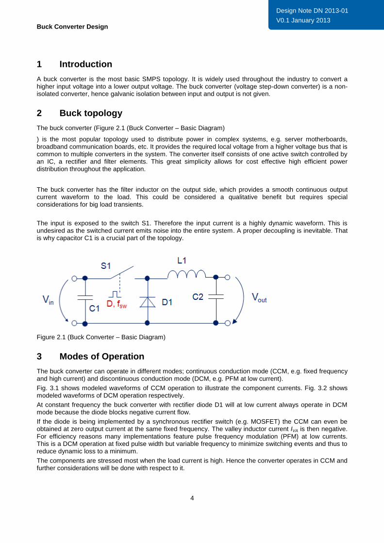
The buck converter (Figure 2.1 (Buck Converter – Basic Diagram)
) is the most popular topology used to distribute power in complex systems, e.g. server motherboards, broadband communication boards, etc. It provides the required local voltage from a higher voltage bus that is common to multiple converters in the system. The converter itself consists of one active switch controlled by an IC, a rectifier and filter elements. This great simplicity allows for cost effective high efficient power distribution throughout the application.
The buck converter has the filter inductor on the output side, which provides a smooth continuous output current waveform to the load. This could be considered a qualitative benefit but requires special considerations for big load transients.
The input is exposed to the switch S1. Therefore the input current is a highly dynamic waveform. This is undesired as the switched current emits noise into the entire system. A proper decoupling is inevitable. That is why capacitor C1 is a crucial part of the topology.
Figure 2.1 (Buck Converter – Basic Diagram)
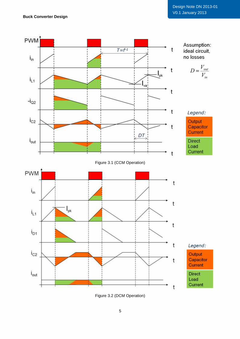
3 Modes of Operation
The buck converter can operate in different modes; continuous conduction mode (CCM, e.g. fixed frequency and high current) and discontinuous conduction mode (DCM, e.g. PFM at low current).
Fig. 3.1 shows modeled waveforms of CCM operation to illustrate the component currents. Fig. 3.2 shows modeled waveforms of DCM operation respectively.
At constant frequency the buck converter with rectifier diode D1 will at low current always operate in DCM mode because the diode blocks negative current flow.
If the diode is being implemented by a synchronous rectifier switch (e.g. MOSFET) the CCM can even be obtained at zero output current at the same fixed frequency. The valley inductor current IVA is then negative. For efficiency reasons many implementations feature pulse frequency modulation (PFM) at low currents. This is a DCM operation at fixed pulse width but variable frequency to minimize switching events and thus to reduce dynamic loss to a minimum.
The components are stressed most when the load current is high. Hence the converter operates in CCM and further considerations will be done with respect to it.
Buck Converter Design
5
Design Note DN 2013-01
V0.1 January 2013
Figure 3.1 (CCM Operation)
Figure 3.2 (DCM Operation)

Buck Converter Design
6
Design Note DN 2013-01
V0.1 January 2013
4 Design Equations
The following are design equations for the CCM operated buck. A design example has been calculated along with the description.
Table 1 Specifications
Input voltage 12 V
Output voltage 1.8 V
Maximum power 120 W
Switching frequency 500 kHz
Inductor current ripple 30%
Output voltage ripple 10 mV
Filter Inductor
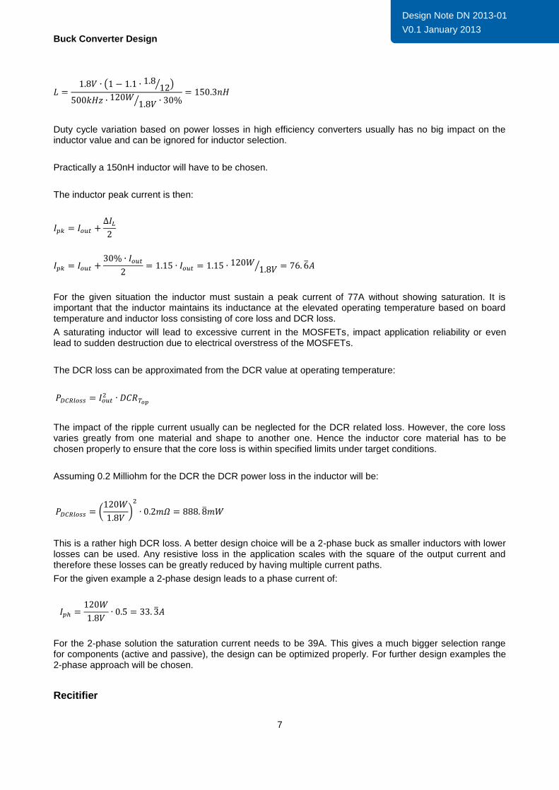
The filter inductor value and its peak current are determined based on the specified maximum inductor current ripple.
For the conditions given in Table 1 the inductor value should be:
When considering a 10% duty cycle increase for offsetting power loss the equation results:
Buck Converter Design
7
Design Note DN 2013-01
V0.1 January 2013
Duty cycle variation based on power losses in high efficiency converters usually has no big impact on the inductor value and can be ignored for inductor selection.
Practically a 150nH inductor will have to be chosen.
The inductor peak current is then:
For the given situation the inductor must sustain a peak current of 77A without showing saturation. It is important that the inductor maintains its inductance at the elevated operating temperature based on board temperature and inductor loss consisting of core loss and DCR loss.
A saturating inductor will lead to excessive current in the MOSFETs, impact application reliability or even lead to sudden destruction due to electrical overstress of the MOSFETs.
The DCR loss can be approximated from the DCR value at operating temperature:
The impact of the ripple current usually can be neglected for the DCR related loss. However, the core loss varies greatly from one material and shape to another one. Hence the inductor core material has to be chosen properly to ensure that the core loss is within specified limits under target conditions.
Assuming 0.2 Milliohm for the DCR the DCR power loss in the inductor will be:
This is a rather high DCR loss. A better design choice will be a 2-phase buck as smaller inductors with lower losses can be used. Any resistive loss in the application scales with the square of the output current and therefore these losses can be greatly reduced by having multiple current paths.
For the given example a 2-phase design leads to a phase current of:
For the 2-phase solution the saturation current needs to be 39A. This gives a much bigger selection range for components (active and passive), the design can be optimized properly. For further design examples the 2-phase approach will be chosen.
Recitifier
Buck Converter Design
8
Design Note DN 2013-01
V0.1 January 2013
The rectifier diode D1 encounters a forward conduction loss of:
For our example that leads to a diode loss of:
One can see from that figure that a synchronous rectifier is inevitable to make this an efficient power converter.
Every Milliohm RDSON in the synchronous rectifier MOSFET accounts for a conduction loss of:
.
The BSC010NE2LS has a typical RDSON of 1 mΩ at 5 V gate drive voltage.
Additional consideration for the synchronous rectifier FET is the reverse recovery loss, dead time loss and the gate drive loss. They all are dynamic properties.
The reverse recovery loss is very hard to determine from the datasheet as it has many dependencies. However, in state-of the art switching MOSFETs it is small so that it usually will not play a primary role in the concrete choice of the MOSFET. Some MOSFETs have implemented embedded reverse recovery free structures bypassing the body diode. Those FETs have an advantage on reverse recovery loss at the expense of RDSON per die area.
A main criteria for low dead time loss is the driver that controls the gate of switching FET and synchronous rectifier MOSFET with minimum time between them.
Dead time loss is directly proportional to the switching frequency:
For the example here we assume a switching frequency of 300kHz and a dead time per transition of 10ns. The forward voltage drop across the body diode is assumed to be 0.8V.
The driving voltage VGSdrive is another critical operation parameter. It impacts the RDSON and switching speed of the MOSFET. Gate charge of the MOSFET and its RDSON are inversely proportional to each other in a given technology. Therefore, an optimal MOSFET depends also on the chosen switching frequency and gate drive voltage.
Also gate charge loss is directly proportional to the switching frequency:
For the example here we have a MOSFET BSC010NE2LS with a gate charge of 34 nC at 5 V gate drive voltage VGS and 12 V VDS.
Buck Converter Design
9
Design Note DN 2013-01
V0.1 January 2013
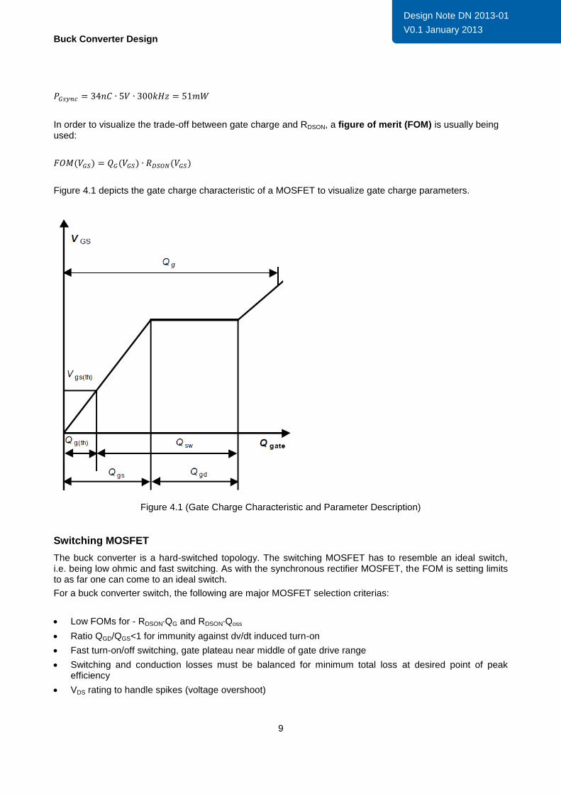
In order to visualize the trade-off between gate charge and RDSON, a figure of merit (FOM) is usually being used:
Figure 4.1 depicts the gate charge characteristic of a MOSFET to visualize gate charge parameters.
Figure 4.1 (Gate Charge Characteristic and Parameter Description)
Switching MOSFET
The buck converter is a hard-switched topology. The switching MOSFET has to resemble an ideal switch, i.e. being low ohmic and fast switching. As with the synchronous rectifier MOSFET, the FOM is setting limits to as far one can come to an ideal switch.
For a buck converter switch, the following are major MOSFET selection criterias:
Low FOMs for - RDSON·QG and RDSON·Qoss
Ratio QGD/QGS<1 for immunity against dv/dt induced turn-on
Fast turn-on/off switching, gate plateau near middle of gate drive range
Switching and conduction losses must be balanced for minimum total loss at desired point of peak efficiency
VDS rating to handle spikes (voltage overshoot)

Buck Converter Design
10
Design Note DN 2013-01
V0.1 January 2013
Low thermal resistance RthJC
Package selection must consider the importance of RthJA
Body diode speed and reverse recovery charge are not important, since body diode rarely conducts in a buck converter (only during forced output voltage down transitions)
The power loss equations for the various losses in the HS-MOSFET are:
Output capacitance Coss is one of the parasitic MOSFET parameters. The output charge related FOMOSS is a means to quantify the impact of dynamic performance among different technologies. In every cycle the output capacitance of the HS-MOSFET will be charged when the HS-FET turns off and annhialated (dissipated within the channel) when the MOSFET turns on. For the BSC050NE2LS at the sample conditions the output capacitance related loss accounts for:
Switching loss for inductively limited switching (fast switching with inductive plateau in switching waveform):
Switching loss for resistively limited switching (slow switching with gate charge plateau in waveform):
with QSW being the switching charge (see fig. 4.1), i.e. the charge that has to be added to transition the MOSFET from the threshold voltage at the gate to the end of the plateau (low VDS) in the gate charge characteristic. RGate represents the total resistance in the gate drive path (including MOSFET and driver) and VGS is the driving voltage. This equation is just a first order approximation as the driving voltage changes during the transition. For centered plateau voltages it still provides a reasonable estimation.
More precise switching losses can be obtained when simulating the transition. In that case the parasitic source inductances of both MOSFETs can be accounted for easily.
For high efficiency the HS-MOSFET should have a low FOM value to provide a low RDSON while switching faster than the current transitions between HS and LS-MOSFET within its commutation loop. In addition the driver must provide sufficiently low sink- and source impedances to drive the MOSFET quickly. For the same reason the gate resistance in the MOSFET must be small as well.
The determination of which method of calculation to apply one must determine if the MOSFET can be enhanced quicker than the drain current can transition:

Buck Converter Design
11
Design Note DN 2013-01
V0.1 January 2013
If is true, then inductively limited switching applies.
For example the BSC050NE2LS is a typical HS-MOSFET in OptiMOS™25V technology. At 5 V gate drive voltage its typical RDSON is 5.5 mΩ. Its gate charge at 5 V with 12 V VDS is 5.5 nC.
Its gate charge FOM for 5V (FOMQG) is 30.25 mΩnC. In a 12 V input converter application with a stray inductance of 1.4 nH and a phase current of 33.3 A, the current transition time limited by the stray inductance is:
The gate resistance of the BSC050NE2LS is 0.5 Ω. Its QGS is 2.2 nC at a plateau voltage of 2.8 V. The threshold voltage is 1.6 V. The turn-on of the HS-MOSFET with a driver of 1 Ω sourcing resistance at 5 V occurs in:
The MOSFET turn on takes less than 1/7th the time of the current transition. Having an appropriate circuit
design without significant source feedback will enable inductively limited switching and thus lowest switching losses. Usually one can see the transitioning between inductively limited switching and resistively limited switching at a sepcific current level at which the spike voltage at the phase node changes qualitatively to a higher value at inductively limited transitions.
Aforementioned inductive source feedback is a very critical design aspect. The package of choice should ideally have no inductive feedback into the gate drive path. Therefore, preferred packages are CanPAK™, Blade-package or any integrated solutions such as DrMOS and DrBlade.
For the example here the switching loss can be calculated as:
Note: When resistively limited losses may partially have to be taken into account.
HS-Loss summary (except reverse recovery loss of LS-MOSFET body diode):
The total loss is about 1.17W. The switching loss is just about ¼ of the conduction loss. As this appears to be highly imbalanced, the BSC050NE2LS is the highest RDSON in that given package and technology. It

Buck Converter Design
12
Design Note DN 2013-01
V0.1 January 2013
allows for higher switching frequency to balance the losses. If that is reasonable depends on the entire converter stage and efficiency targets.
However, the calculations have been done only for 33.3 A output current. The high ratio also ensures that inductively limited switching prevails over a big range to low currents so that efficiency stays high over the entire range.
Gate charge and output charge related losses are small in comparison. They will start to become relevant when taking low current operation into consideration.
LS-loss summary (except reverse recovery loss of LS-MOSFET body diode):
The total loss is about 1.05 W. Therefore, HS-FET and LS-FET RDSON-selection appears to be well chosen with respect to the power loss distribution among these two devices.
Output Capacitor
The function of the output capacitor is to filter the inductor current ripple and deliver a stable output voltage. It also has to ensure that load steps at the output can be supported before the regulator is able to react.
These are two distinct criteria which define the value and concrete design of the output capacitor solution.
Filter criteria 1 (based on filter inductor current ripple for n phases):
is the vector sum of the ripple currents of all phases. The charge change at the output capacitors causing a voltage ripple is:
The voltage at Cout changes with the charge:
Thus, the first criteria for the minimum output capacitance is:
For the given requirements the minimum output capacitance according to criteria 1 is:

Buck Converter Design
13
Design Note DN 2013-01
V0.1 January 2013
Filter criteria 2 (load step support):
Every phase can support a current transient of:
Having a required load transient of
for the application, the regulator can only support a transient of
, even with an immediate response. For the difference
the current has to be supported
by the output capacitor for the ramping time tramp.
The voltage drop at the output capacitor is:
The charge supplied by all phases accounts for:
The charge that needs to be supplied by the output capacitor is:
with
The absolute value of the output voltage drop at a load step of ΔIout in tStep is then:
The requirement for Cout according to criteria 2 is:

Buck Converter Design
14
Design Note DN 2013-01
V0.1 January 2013
For example, a load step of 20A/20us on a maximum duty cycle of 50% requires a minimum output capacitance for a permitted voltage drop of 50mV of:
In case of a negative result the transient can fully be supported by the duty cycle change.
Assuming a load step of 20A/2ns requires:
Conclusion for output capacitor selection:
Comparing the calculated values of criteria 1 and 2 leads to the conclusion that criteria 1 is imposing the more stringent constraints. The output capacitance is determined by criteria 1.
This result is an electrical value which is required under the assumption that the response of the regulator is immediate and simultaneous on all phases. This is normally not the case and has to be considered. Also, capacitors have a big tolerance usually below its nominal value. Deratings for DC bias and temperature have to be taken into account too.
Input Capacitor
The function of the input capacitor is to filter the input current into the regulator – ideally it should appear as a DC current for steady state load conditions.
When filtered ideally, the DC input current is:
Ignoring the ripple effect, the current in one switch during its on-time is:
The charge to be stored in the input capacitor has to compensate for the difference between switched current and DC input current.
with
Hence the minimum value for the input decoupling capacitor should not be less than:
Buck Converter Design
15
Design Note DN 2013-01
V0.1 January 2013
where dVin is the permissible voltage ripple at the input capacitor.
The current in the input capacitor is a critical design criteria for selecting the capacitors. Capacitors have an
intrinsic serial resistance (ESR) which causes conduction loss and heating impacting long term reliability of
electrolyte based capacitors.
The RMS current for the entire input capacitor bank is:
Thermals and Package
MOSFETs come in a broad variety of packages. For a decision the following aspects hasve to be taken into account:
- Required RDSON determines minimum package size.
- Fast switching (inductively limited) is only possible in packages with low inductive source feedback.
- Package resistance should be small to enable good FOM of the device (very important for low RDSON-MOSFETs).
- Thermal resistance of package to cooling path must be sufficiently small. If cooling to top side is required a package with low RthJCtop has to be chosen.
- In some cases thermal transient performance is important. In that case packages with big leadframes under the die are usually the preferred choice.
From the power loss in the MOSFET and the permitted temperature rise of its junction to ambient the required thermal resistance to ambient RthJA can be calculated:
with
The thermal package resistance RthJC is given in the datasheet. For power MOSFETs (TO, SuperSO-8, S3O8, CanPAK packages) this number is usually below 5 K/W, in cases where the die fills out the package quite well the numbers are in the vicinity of 1 K/W. A temperature rise of 50 K under operating conditions would allow for 5 W power loss in the MOSFET with 5 K/W thermal resistance to case - given the pcb is equal to ambient temperature. This, however, is rarely the case. The determining and mostly limiting factor is the thermal resistance case to ambient. Criterias defining this number are barely influenced by the package choice.
- Board size
- Air flow
- Heatsink (RthJCtop is important to make effective use of the heatsink)
- Layer stack and design (copper thickness, closed copper layers and thermal vias, exposed copper area on top and bottom layers)
- Interface area between package and board.

Buck Converter Design
16
Design Note DN 2013-01
V0.1 January 2013
The last point of interface area and especially outline length of the thermal pad of the power MOSFET on the PCB is particularly important when thermal vias under the pad are missing and when the copper thickness of the top layer is small. In that case a big difference of total thermal resistance RTHJA can be seen between S3O8 and SSO-8, which is simply bigger. The heat has to be transported from the package outline to the PCB. A small outline has a higher resistance. This becomes significant when other paths for thermal transport are missing (vias in pad or thick copper on top layer to offset small outline).
For transient thermal analysis L3 – PSpice models of the MOSFETs can be used. They incorporate a thermal network describing the heat transfer characteristic through the die and the package. These models provide access to TJ and TC so that external thermal networks can be established.
For example, a definition in PSpice as subcircuit for a CanPAK 25V MOSFET is initiated by:
.SUBCKT BSB012NE2LX drain gate source Tj Tcase PARAMS: dVth=0 dRdson=0 dgfs=0 dC=0 Zthtype=0 Ls=0.05n Ld=0.7n Lg=0.1n
Highlighted are the 5 terminals ‘drain’, ‘gate’, ‘source’, ‘Tj’, Tcase’ and the parameters for package inductances ‘Ls’, Ld’ and ‘Lg’. It can be seen that the dominant inductance is drain inductance. This package supports fast switching and top-side cooling.
Note that the actual inductance in the application varies from the default values as mutual inductances occur. This is especially important for the commutation loop in which the MOSFETs are located.

Buck Converter Design
17
Design Note DN 2013-01
V0.1 January 2013
Symbols used in formulas
D, Dmax duty cycle, maximum duty cycle
ESR capacitor series resistance
fsw, f switching frequency
FOM figure of merit
IVA, IPK inductor valley current, inductor peak current
ISW, Iph current in switch, phase current
Iout, Iavg output current, average current
ICinRMS input capacitor RMS current
L1, L1, L output inductor
LStray stray inductance
n phase count
Psync_on resistive loss in synchronous rectifier MOSFET
PVFD1 diode conduction loss in D1
Ptdead dead time loss
PGsync gate drive loss of synchronous rectifier MOSFET
PDCRloss inductor DCR loss
PHScond conduction loss of HS-MOSFET
PHS_Gate gate drive loss of HS-MOSFET
Poss_HS output capacitance loss of HS-MOSFET
PSW_HS switching loss of HS-MOSFET
Pcaploss capacitor loss
PMOSFET MOSFET power loss
QGS, QGS_HS MOSFET gate -source charge, HS-MOSFET gate-source charge
QGD gate-drain charge of MOSFET
Qsw MOSFET switching charge
QG total gate charge of MOSFET
QGsync gate charge of synchronous rectifier MOSFET
Qoss output charge of MOSFET
RthJA, RthJC thermal resistance junction to ambient, thermal resistance junction to case
RthCA thermal resistance case to ambient
RDSON, RDSON_HS on-resistance of MOSFET, on-resistance of HS-MOSFET
RGate gate resistance
Tsw, T switching period
Tj, TA junction temperature, ambient temperature
tinductive current commutation time during inductively limited switching
tresistive current commutation time during resistively limited switching
tstep time of an output load step
tramp time to ramp up the current in the regulator inductors
Vin, Vout input voltage, output voltage
VGS, VGS_HS gate-to-source driving voltage of MOSFET, gate-to-source driving voltage of HS-MOSFET
VplatHS, VthHS plateau voltage of HS-MOSFET, threshold voltage of HS MOSFET
ΔIL, ΔICout inductor ripple current, output capacitor ripple current
ΔQCout output capacitor charge variation
ΔQnph charge change delivered by n-phases of the regulator
ΔQout charge change at output during load step
ΔVout output voltage ripple
η efficiency
dQcapmin min. charge to be stored in input capacitor