design and implementation of a multiphase buck converter
TRANSCRIPT

Design and Implementation of a Multiphase Buck Converter for
Front End 48V-12V Intermediate Bus Converters
Christopher Xavior Salvo
Thesis submitted to the faculty of the Virginia Polytechnic Institute and State University in
partial fulfillment of the requirements for the degree of
Master of Science
In
Electrical Engineering
Rolando Burgos (Chair)
Qiang Li
Dushan Boroyevich
6/4/2019
Blacksburg, VA
Keywords: Multiphase Buck, Planar Magnetics, Average Current Mode Control, Intermediate
Bus Converter, Gallium Nitride, Two-Stage Converter

Design and Implementation of a Multiphase Buck Converter for
Front End 48V-12V Intermediate Bus Converters
Christopher Xavior Salvo
Abstract
The trend in isolated DC/DC bus converters is increasing the output power in the same
brick form factors that have been used in the past. Traditional intermediate bus converters (IBCs)
use silicon power metal oxide semiconductor field effect transistors (MOSFETs), which recently
have reached the limit in terms of turn on resistance (RDSON) and switching frequency. In order to
make the IBCs smaller, the switching frequency needs to be pushed higher, which will in turn
shrink the magnetics, lowering the converter size, but increase the switching related losses,
lowering the overall efficiency of the converter. Wide-bandgap semiconductor devices are
becoming more popular in commercial products and gallium nitride (GaN) devices are able to push
the switching frequency higher without sacrificing efficiency. GaN devices can shrink the size of
the converter and provide better efficiency than its silicon counterpart provides.
A survey of current IBCs was conducted in order to find a design point for efficiency and
power density. A two-stage converter topology was explored, with a multiphase buck converter as
the front end, followed by an LLC resonant converter. The multiphase buck converter provides
regulation, while the LLC provides isolation. With the buck converter providing regulation, the
switching frequency of the entire converter will be constant. A constant switching frequency
allows for better electromagnetic interference (EMI) mitigation.

This work includes the details to design and implement a hard-switched multiphase buck
converter with planar magnetics using GaN devices. The efficiency includes both the buck
efficiency and the overall efficiency of the two-stage converter including the LLC. The buck
converter operates with 40V - 60V input, nominally 48V, and outputs 36V at 1 kW, which is the
input to the LLC regulating 36V – 12V. Both open and closed loop was measured for the buck
and the full converter. EMI performance was not measured or addressed in this work.

Design and Implementation of a Multiphase Buck Converter for
Front End 48V-12V Intermediate Bus Converters
Christopher Xavior Salvo
General Audience Abstract
Traditional silicon devices are widely used in all power electronics applications today,
however they have reached their limit in terms of size and performance. With the introduction of
gallium nitride (GaN) field effect transistors (FETs), the limits of silicon can now be passed with
GaN providing better performance. GaN devices can be switched at higher switching frequencies
than silicon, which allows for the magnetics of power converters to be smaller. GaN devices can
also achieve higher efficiency than silicon, so increasing the switching frequency will not hurt the
overall efficiency of the power converter. GaN devices can handle higher switching frequencies
and larger currents while maintaining the same or better efficiencies over their silicon counterparts.
This work illustrates the design and implementation of GaN devices into a multiphase buck
converter. This converter is the front end of a two-stage converter, where the buck will provide
regulation and the second stage will provide isolation. With the use of higher switching
frequencies, the magnetics can be decreased in size, meaning planar magnetics can be used in the
power converter. Planar magnetics can be placed directly inside of the printing circuit board
(PCB), which allows for higher power densities and easy manufacturing of the magnetics and
overall converter. Finally, the open and closed loop were verified and compared to the current
converters that are on the market in the 48V – 12V area of intermediate bus converters (IBCs).

v
Acknowledgements
I would like to take this opportunity to thank my advisor Dr. Rolando Burgos, for his
support and guidance through my experience in the Center for Power Electronics Systems (CPES).
Dr. Burgos also helped guide me toward power electronics during my undergraduate tenure at
Virginia Tech and without that, I would never be here. I would also like to thank Dr. Burgos for
recommending me for the Wide-Bandgap fellowship sponsored by the US Department of Energy.
I would also like to thank Dr. Qiang Li for his guidance throughout my project and the classes that
he taught throughout graduate school, providing me with the knowledge I needed for my Master’s.
I would also like to thank Bingyao Sun and Mohamed Ahmed for supporting me
throughout my graduate schooling. Without them I would not have completed my Master’s in a
timely manner. Their expertise about planar magnetics and power electronics in general provided
me with the knowledge I needed to complete this project.
I would like to thank Tom Byrd, Tyler Parks, Joshua Baer, Clint Gnegy, and Dennis
Reinhardt from Lockheed Martin. Without them, there would be no project. Their expertise from
industry helped guide me in my design of this converter. I would also like to thank Brandon
Witcher from VPT, whose expertise in implementation was a tremendous help in the design of the
converter.
I would like to thank Marianne Hawthorne, Linda Long, Lauren Shutt, Teresa Shaw, David
Gilham, and Na Ren for their help and support for anything else that I needed to complete my
project.
Finally, I would like to thank all of my friends that I have made in CPES and all of the
people that I worked with. Thanks for making my time at Virginia Tech memorable and enjoyable.

vi
Table of Contents
Chapter 1. Introduction ................................................................................................................... 1
1.1 Background ........................................................................................................................... 1
1.2 Intermediate Bus Converter Topology .................................................................................. 2
1.3 Benefits of Gallium Nitride over Silicon .............................................................................. 3
1.4 Thesis Outline ....................................................................................................................... 6
Chapter 2. Topology Selection of Buck Converter ......................................................................... 7
2.1 System Specifications ........................................................................................................... 7
2.2 Device Selection .................................................................................................................. 10
2.3 Electro-Thermal Design ...................................................................................................... 25
2.4 Topology Evaluation ........................................................................................................... 32
Chapter 3. Planar Magnetics Design ............................................................................................. 37
3.1 Magnetics Structure and Background ................................................................................. 37
3.2 Design of Inductors: Two-Phase Coupled Inductor for Four-Phase Buck.......................... 47
3.3 Design of Inductors: Two-Phase Coupled Inductor for Two-Phase Buck .......................... 90
3.4 Design of Inductors: Normal Inductor for Four-Phase Buck .............................................. 96
3.5 Evaluation of Inductors ..................................................................................................... 111
Chapter 4. Control System Design.............................................................................................. 118
4.1 Controller Selection........................................................................................................... 118
4.2 Open Loop Small Signal Analysis .................................................................................... 121
4.3 Closed Loop Design for Voltage Mode Control ............................................................... 140
4.4 Average Current Mode Control Analysis.......................................................................... 150
4.5 Control Method Comparison and Selection ...................................................................... 165
Chapter 5. Prototype Design and Construction........................................................................... 168
5.1 Circuit Layout ................................................................................................................... 168
5.2 Gate Driver Layout............................................................................................................ 170
5.3 Inductor Layout ................................................................................................................. 175
5.4 Cooling System ................................................................................................................. 182
5.5 Functional Open Loop Testing .......................................................................................... 184
Chapter 6. Experimental Evaluations ......................................................................................... 194
6.1 Buck Converter Results ..................................................................................................... 194
6.2 Two-Stage Results............................................................................................................. 208

vii
6.3 Steady State and Transient Response for Closed Loop Buck ........................................... 211
Chapter 7. Conclusions ............................................................................................................... 228
7.1 Conclusions from Magnetics Design ................................................................................ 228
7.2 Conclusions from Power Stage and Layout ...................................................................... 231
7.3 Prospective Areas for Future Research ............................................................................. 232
Appendix A – MATLAB Optimization Code for Inductors ....................................................... 235
Code for Four-Phase Buck Converter Design Coupled Inductors .......................................... 235
Code for Two-Phase Buck Converter Coupled Inductor ........................................................ 246
Code for Four-Phase Buck Normal Inductors ......................................................................... 257
Inductance Minimization Script .............................................................................................. 262
Appendix B – Small Signal Coefficients .................................................................................... 264
References ................................................................................................................................... 266

viii
List of Figures
Figure 1.1 - Google's Data Center Power Architecture .................................................................. 1
Figure 1.2 - RDSON Comparison between Semiconductors ............................................................. 4
Figure 1.3 - Gate Capacitance and RDSON vs. Drain to Source Voltage ......................................... 5
Figure 2.1 - EPC GaN Devices ..................................................................................................... 11
Figure 2.2 - Double Pulse Test in LTSPICE................................................................................. 12
Figure 2.3 - Double Pulse Test Gate and Current Waveform ....................................................... 14
Figure 2.4 - Turn On and Turn Off Power .................................................................................... 15
Figure 2.5 - Turn Off Energy and Turn On Energy ...................................................................... 15
Figure 2.6 - Turn On Energy Comparison between Devices ........................................................ 16
Figure 2.7 - Turn Off Energy Comparison between Devices ....................................................... 17
Figure 2.8 - Two-Phase Efficiency Device Comparison .............................................................. 20
Figure 2.9 - Three-Phase Efficiency Device Comparison ............................................................ 21
Figure 2.10 - Four-Phase Efficiency Device Comparison ............................................................ 22
Figure 2.11 - Two-Phase Efficiency Paralleled Devices .............................................................. 23
Figure 2.12 - Topology Loss Comparison .................................................................................... 24
Figure 2.13 - EPC9078 Development Board ................................................................................ 26
Figure 2.14 - Single Phase Buck Schematic ................................................................................. 27
Figure 2.15 - Development Board Buck Converter Waveforms .................................................. 28
Figure 2.16 - Thermal Image of Development Board ................................................................... 29
Figure 2.17 - Device Loss vs Temperature ................................................................................... 30
Figure 2.18 - Optimal GaN Layout ............................................................................................... 33
Figure 2.19 - Optimal Power Loop for GaN Devices ................................................................... 34
Figure 2.20 - Preliminary Four-Phase Interleaved Topology ....................................................... 34
Figure 2.21 - Two-Phase Topology with Paralleled Devices Preliminary Layout ....................... 36
Figure 3.1 - Magnetic Materials for Inductor ............................................................................... 39
Figure 3.2 - Inverse Coupled Inductor EI Core ............................................................................ 41
Figure 3.3 - Direct Coupling versus Inverse Coupling ................................................................. 42
Figure 3.4 - Direct vs Inverse Coupling B-Field Comparison ...................................................... 44
Figure 3.5 - Board Layout with Inductor Size .............................................................................. 47
Figure 3.6 - Front View of Inductor.............................................................................................. 48
Figure 3.7 - BH Curve of 3F36 ..................................................................................................... 49

ix
Figure 3.8 - Magnetic Circuit for Coupled Inductor ..................................................................... 51
Figure 3.9 - Core Loss Density vs Temperature for 3F36 ............................................................ 57
Figure 3.10 - Average Length of Winding.................................................................................... 60
Figure 3.11 - Current Direction in ANSYS Maxwell ................................................................... 61
Figure 3.12 - Winding Groupings ................................................................................................. 62
Figure 3.13 - FR at Different Number of Turns ............................................................................ 65
Figure 3.14 - FR at Different Frequencies ..................................................................................... 66
Figure 3.15 - Magnetic Optimization Flow Chart ........................................................................ 68
Figure 3.16 - Loss per Phase at Different Inductor Depths .......................................................... 69
Figure 3.17 - Loss vs. Core Depth and Efficiency vs. Power Density ......................................... 71
Figure 3.18 - Loss Breakdown at Varying Depths ....................................................................... 72
Figure 3.19 - Inductance vs Varying Depth .................................................................................. 73
Figure 3.20 - Coupling Coefficient vs Varying Depth ................................................................. 74
Figure 3.21 - DC Winding Resistance vs Inductance ................................................................... 75
Figure 3.22 - Coupling Coefficient vs Inductance ........................................................................ 76
Figure 3.23 - Center Leg Width vs Inductance ............................................................................. 77
Figure 3.24 - Inductor Loss per Phase vs Inductance ................................................................... 79
Figure 3.25 - Loss Breakdown at Varying Depths with Different Frequencies ........................... 80
Figure 3.26 - Power Density vs Efficiency at Different Frequencies ........................................... 81
Figure 3.27 - Loss Breakdown vs Inductor Depth at Various Leg Widths ................................... 82
Figure 3.28 - Loss Breakdown at Varying Depths with Different Turns ..................................... 83
Figure 3.29 - Power Density vs Efficiency at Different Turns Number ....................................... 85
Figure 3.30 - Loss Breakdown vs Inductor Depth for Interleaved Windings ............................... 86
Figure 3.31 - Coupling Coefficient vs Inductor Depth ................................................................. 87
Figure 3.32 - Inductance vs Varying Core Depth for Interleaved Windings ................................ 88
Figure 3.33 - Efficiency vs Power Density of Interleaved Windings ........................................... 89
Figure 3.34 - Power Density vs Efficiency Overall Comparison ................................................. 90
Figure 3.35 - Loss per Phase for Two-Phase Coupled Inductor ................................................... 91
Figure 3.36 - Loss Breakdown vs Varying Depth or Two-Phase Coupled Inductor .................... 92
Figure 3.37 - Inductance vs Varying Depth for Two-Phase Coupled Inductor ............................ 93
Figure 3.38 - Total Loss and Efficiency of vs Size of Two-Phase Inductor ................................. 94
Figure 3.39 - Power Density vs Efficiency Comparison .............................................................. 95
Figure 3.40 - Normal Inductor Layout Example .......................................................................... 97

x
Figure 3.41 - Normal Inductor Cross Section ............................................................................... 98
Figure 3.42 - Top Cross Section of Normal Inductor ................................................................... 99
Figure 3.43 - Normal Inductor Magnetic Equivalent Circuit ..................................................... 101
Figure 3.44 - FR Values for the Normal Inductor ....................................................................... 103
Figure 3.45 - Magnetic Flux Density for Normal Inductor ........................................................ 104
Figure 3.46 - Optimization for the Normal Inductor .................................................................. 106
Figure 3.47 - Normal Inductor Loss per Phase ........................................................................... 107
Figure 3.48 - Center Post Diameter versus Winding Width ....................................................... 108
Figure 3.49 - Power Density vs Efficiency for Normal Inductor ............................................... 109
Figure 3.50 - Power Density vs Efficiency for All Designs ....................................................... 111
Figure 3.51 - Power Density vs Efficiency of Different Switching Frequencies ....................... 114
Figure 3.52 - Front View of Coupled Inductor ........................................................................... 116
Figure 3.53 - Side View of Coupled Inductor............................................................................. 117
Figure 3.54 - Top View of Coupled Inductor ............................................................................. 117
Figure 4.1 - Multiphase Controller Comparison ......................................................................... 119
Figure 4.2 - Small Signal Model for Single Phase Buck ............................................................ 122
Figure 4.3 - Equivalent Small Signal Models of Buck Converter .............................................. 124
Figure 4.4 - Frequency Response of Control to Output of the Buck Converter ......................... 125
Figure 4.5 - Equivalent Small Signal Model for Interleaved Buck with Coupled Inductor ....... 126
Figure 4.6 - Circuit Model of the LLC ....................................................................................... 127
Figure 4.7 - Equivalent Circuit Model for LLC .......................................................................... 128
Figure 4.8 - Input-to-Output Frequency Response of LLC ........................................................ 130
Figure 4.9 - Equivalent Small Signal Model for LLC at fs ≥ fo ................................................. 131
Figure 4.10 - Simplified Equivalent Small Signal Model for LLC at fs ≥ fo ............................. 132
Figure 4.11 - Input-to-Output Frequency Response of LLC Circuit Comparison ...................... 133
Figure 4.12 - Two-Stage Small Signal Model ............................................................................ 134
Figure 4.13 - Simplified Two-Stage Small Signal Model .......................................................... 135
Figure 4.14 - Small Signal Model in SIMPLIS .......................................................................... 136
Figure 4.15 - Control-to-Output Comparison of Small Signal Model and Simulation .............. 137
Figure 4.16 - Small Signal Model with Magnetizing Inductance ............................................... 138
Figure 4.17 - Frequency Response of Control-to-Output of Two-Stage Converter ................... 139
Figure 4.18 - Type-III Compensator ........................................................................................... 141
Figure 4.19 - Sisotool Bode Editor for Control-to-Output Transfer Function ............................ 144

xi
Figure 4.20 - Closed Loop Small Signal Model Comparison ..................................................... 146
Figure 4.21 - Full Circuit for Transient Analysis ....................................................................... 148
Figure 4.22 - Load Step Up......................................................................................................... 149
Figure 4.23 - Load Step Down .................................................................................................... 150
Figure 4.24 - Current Loop for LM-5170 ................................................................................... 152
Figure 4.25 - Closed Voltage Loop for LM-5170....................................................................... 154
Figure 4.26 - Small Signal Model for LM-5170 ......................................................................... 156
Figure 4.27 - Bode Plot of Closed Voltage Loop for LM-5170 Design Sheet ........................... 158
Figure 4.28 - Bode Plot of Closed Voltage Loop with SIMPLIS Circuit ................................... 159
Figure 4.29 - Two-Stage Closed Voltage Loop with Average Current Mode Control............... 160
Figure 4.30 - Two-Stage Closed Loop with Average Current Mode Control ............................ 161
Figure 4.31 - Load Step Up - Average Current Mode Control ................................................... 162
Figure 4.32 - Load Step Down - Average Current Mode Control .............................................. 163
Figure 4.33 - Control Signals for Average Current Mode Control ............................................. 164
Figure 4.34 - Comparison of Transient between Voltage and Current Control .......................... 165
Figure 5.1 - Preliminary Two-Stage Layout ............................................................................... 169
Figure 5.2 - Optimal Loop for GaN Devices .............................................................................. 171
Figure 5.3 - Top Layer Gate Driver Layout ................................................................................ 172
Figure 5.3 - 3D Rendering of Gate Driver Layout ...................................................................... 173
Figure 5.4 - Four-Phase Gate Layout .......................................................................................... 174
Figure 5.5 - Cross Sectional View of Coupled Inductor ............................................................. 176
Figure 5.6 - Winding Connection for Coupled Inductor ............................................................. 176
Figure 5.7 - Current Distribution in the Inductor Windings ....................................................... 177
Figure 5.8 - New Winding Connection for Coupled Inductor .................................................... 178
Figure 5.9 - Current Distribution for New Winding Structure ................................................... 179
Figure 5.10 - Winding Connection for Inductor (1) ................................................................... 180
Figure 5.11 - Winding Connection for Inductor (2) ................................................................... 181
Figure 5.12 - Top View of Buck Converter Layout.................................................................... 182
Figure 5.13 - Direction of Air Flow on Buck Converter ............................................................ 184
Figure 5.14 - Inductance Measurement Setup ............................................................................ 185
Figure 5.15 - Dead Time Generation Circuit .............................................................................. 187
Figure 5.16 - High Side Gate Signal ........................................................................................... 189
Figure 5.17 - Low Side Gate Signal............................................................................................ 190

xii
Figure 5.18 - Equipment for Open Loop Testing ....................................................................... 192
Figure 5.19 - Open Loop Setup for Buck Converter .................................................................. 193
Figure 6.1 - Capacitance vs DC Bias .......................................................................................... 196
Figure 6.2 - Low Side Gate Signals (1) ...................................................................................... 197
Figure 6.3 - Low Side Gate Signals (2) ...................................................................................... 198
Figure 6.4 - Inductor Current for Phases One and Two .............................................................. 199
Figure 6.5 - 48V Open Loop Waveforms ................................................................................... 200
Figure 6.6 - Open Loop Efficiency Comparison at 48V ............................................................. 201
Figure 6.7 - 60V Open Loop Waveforms ................................................................................... 202
Figure 6.8 - Open Loop Efficiency Comparison at 60V ............................................................. 203
Figure 6.9 - 40V Open Loop Waveforms ................................................................................... 204
Figure 6.10 - Open Loop Efficiency Comparison at 40V ........................................................... 205
Figure 6.11 - Measured Open Loop Efficiency Comparison ...................................................... 206
Figure 6.12 - Thermal Image of Buck at 48V Input ................................................................... 207
Figure 6.13 - Two-Stage Converter ............................................................................................ 209
Figure 6.14 - Open Loop Two-Stage Efficiency at 48V ............................................................. 210
Figure 6.15 - Top and Bottom Layer of LM-5170 Board ........................................................... 211
Figure 6.16 - Startup Waveform for Buck Converter ................................................................. 213
Figure 6.17 - Steady State Waveforms for Buck Converter ....................................................... 214
Figure 6.18 - Steady State Switching Node Voltages (1) ........................................................... 215
Figure 6.19 - Steady State Switching Node Voltages (2) ........................................................... 217
Figure 6.20 - Thermal Image of Closed Loop Buck at 1 kW ..................................................... 218
Figure 6.21 - ISETA Signals ....................................................................................................... 220
Figure 6.22 - Thermal Image of Limited Current on Controller 1 .............................................. 222
Figure 6.23 - Compensation Circuit for ESL of Sense Resistor ................................................. 224
Figure 6.24 - Load Step Up Buck Converter (500W → 1000W) ............................................... 226
Figure 6.25 - Load Step Down Buck Converter (1000W → 500W) .......................................... 227

xiii
List of Tables
Table 1.1 - System Specifications ................................................................................................... 8
Table 2.1 - Top Device Loss Topology vs Frequency .................................................................. 31
Table 3.1 - Material Coefficients for 3F36 ................................................................................... 56
Table 3.2 - Inductor Design Dimensions .................................................................................... 115
Table 4.1 - Compensator Components for Voltage Mode Control ............................................. 146
Table 4.2 - Compensator Components for Current and Voltage Loop ....................................... 157
Table 4.3 - Compensator Components for Current and Voltage Loop Two-Stage .................... 161
Table 4.4 - Closed Loop Characteristic Comparison .................................................................. 166
Table 5.1 - Measured Inductance Values .................................................................................... 186
Table 5.2 - Dead Time Resistor Values ...................................................................................... 191
Table 6.1 - Buck Converter Circuit Parameters .......................................................................... 195

1
Chapter 1. Introduction
1.1 Background
Intermediate bus architectures using 48V bus converters are widely used in telecom,
wireless networks, servers, and data centers. Fig. 1.1 shows the bus architecture that Google is
employing into its data centers and where the 48V intermediate bus converter (IBC) would be
located. There is a rapid increase in load demand, so there is a need for higher power converters
and with high power densities and efficiencies. There are three types of bus converters:
unregulated, semi-regulated, and fully regulated bus converters. Unregulated converters are used
for narrow input ranges (40V-60V) that step down to a second stage point of load (POL) converter
that will regulate to output voltage [1][2]. The semi-regulated bus converter uses a wider input
range (36V-75V) which is then converted to a small output range, in which a POL converter can
tightly regulate the final output [3][4]. The fully regulated takes the same input ranges as the other
two bus converters and tightly regulates output, so the POL has a constant input voltage [5][6].
The focus of this thesis will be on the fully regulated bus converter.
Figure 1.1 - Google's Data Center Power Architecture

2
1.2 Intermediate Bus Converter Topology
The common practice for bus converters is by using pulse width modulation (PWM) at a
constant frequency in either a single-stage [6] or a two-stage solution [3]. The benefit of a single-
stage IBC is that the efficiency will be higher because the power transfer does not go through two
separate converters. The drawback to single-stage converters is that they are resonant converters
and to control resonant converters, the switching frequency has to be variable. In some
applications, this is acceptable, but in others, the EMI impact can to large. Some typical single
stage topologies in the phase shifted full bridge (PSFB) converter and LLC converter. The PSFB
is a constant frequency buck converter with a transformer that has a wide range of powers and
input and output voltages. The main drawback of the PSFB in the class of 48V/12V IBCs is that
when the output power increases, a single MOSFET cannot hold the current of the output, so the
solution is to parallel MOSFETs on the output terminal and parallel windings in the transformer.
This will solve the issue, but introduce current imbalance among the synchronous rectifiers.
Another issue with low voltage high current converters is that the termination loss between AC
points on the transformer is large. With larger current on the output, the switching frequency needs
to be lower, so the synchronous rectifiers do cause too much loss for the overall converter
efficiency. With lower switching frequency, the magnetics will be larger and can hurt the overall
power density of the converter. There are solutions to these problems discussed in [7], but the
transformer takes careful design consideration and the control method is difficult to implement.
The benefit for two-stage PWM converters is that the switching frequency is constant, so
the EMI impact is predictable and can be filtered easily if both stages are using the same beat
frequencies. Using a PWM converter greatly simplifies the control method. There are many
control methods for PWM converters that have been studied in depth and are easy to implement.

3
In the case of a two-stage converter, the first stage could provide regulation, while the second stage
provides isolation or vice-versa. In both cases the voltage will be stepped down, so a converter
that can handle high power will be necessary. For example, a buck converter can be used as the
first stage to provide isolation, while the second stage can be any converter that can isolate the
power. With a buck converter as the first stage, the control methods are well known and easily
implementable. The drawback is that one may not be able to achieve the same efficiency as a
single stage converter. To achieve a high efficiency with a two-stage converter, both stage will
need to have high efficiencies (>97%) to even be comparable to a single stage, due to the
multiplicative efficiency calculation.
1.3 Benefits of Gallium Nitride over Silicon
Up until recently, silicon has been the semiconductor of choice when producing power
devices due to its easy manufacturability and intrinsic properties. However, with recent advances
in device technology, wide bandgap semiconductors have come to be more popular in modern
power converters. Wide bandgap semiconductors are different from silicon by having a larger
distance between the valence and conduction band, hence the name wide bandgap. The two most
popular wide bandgap devices are silicon carbide (SiC) and gallium nitride (GaN). SiC metal
oxide semiconductor field effect transistors (MOSFETs) are used in higher voltage applications,
typically greater than 1 kV, where as GaN MOSFETs are used in the range of 100V to 650V.
Wide bandgap devices provide the benefit of having lower turn on resistance (RDSon) and smaller
gate capacitance (QGD) [8]. Both of these parameters combined allow power converters to be
pushed to higher switching frequencies without sacrificing large switching and conduction losses
on the devices.
4
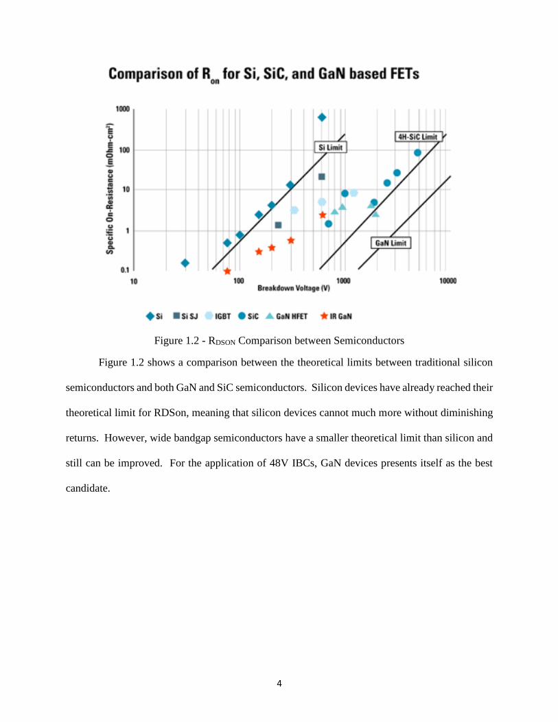
Figure 1.2 - RDSON Comparison between Semiconductors
Figure 1.2 shows a comparison between the theoretical limits between traditional silicon
semiconductors and both GaN and SiC semiconductors. Silicon devices have already reached their
theoretical limit for RDSon, meaning that silicon devices cannot much more without diminishing
returns. However, wide bandgap semiconductors have a smaller theoretical limit than silicon and
still can be improved. For the application of 48V IBCs, GaN devices presents itself as the best
candidate.
5
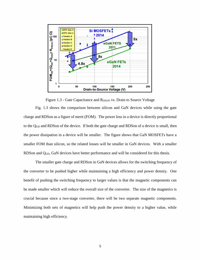
Figure 1.3 - Gate Capacitance and RDSON vs. Drain to Source Voltage
Fig. 1.3 shows the comparison between silicon and GaN devices while using the gate
charge and RDSon as a figure of merit (FOM). The power loss in a device is directly proportional
to the QGD and RDSon of the device. If both the gate charge and RDSon of a device is small, then
the power dissipation in a device will be smaller. The figure shows that GaN MOSFETs have a
smaller FOM than silicon, so the related losses will be smaller in GaN devices. With a smaller
RDSon and QGD, GaN devices have better performance and will be considered for this thesis.
The smaller gate charge and RDSon in GaN devices allows for the switching frequency of
the converter to be pushed higher while maintaining a high efficiency and power density. One
benefit of pushing the switching frequency to larger values is that the magnetic components can
be made smaller which will reduce the overall size of the converter. The size of the magnetics is
crucial because since a two-stage converter, there will be two separate magnetic components.
Minimizing both sets of magnetics will help push the power density to a higher value, while
maintaining high efficiency.

6
1.4 Thesis Outline
The focus of this thesis is to discuss the design process and implementation of the front
end converter for a two-stage IBC. The front end will consist of a buck converter that feeds into
the second stage, which is an LLC converter. The two-stage converter should be useful in a variety
of IBAs where EMI performance is critical. Topology comparison, magnetics design, closed loop
design, and experimental evaluation will be discussed in a comprehensive manner.
Chapter 1 includes the motivation behind making an IBC capable of pushing higher power
than what is commercially available. The current topologies are discussed with benefits and
drawbacks both discussed for both single-stage and two-stage configurations. The benefits of GaN
devices are shown in comparison to silicon devices and an explanation is given why GaN devices
will be used in the converter design to achieve high efficiency and power density.
Chapter 2 discusses topology selection for the front end of the IBC. The first stage is a
buck converter, so the various interleaving strategies are compared to see which will give the best
efficiency and highest power density. The devices are selected in addition with an electro-thermal
analysis to determine what devices will give the least loss in the selected topologies.
Chapter 3 consists of the magnetics design for the buck converter. Planar magnetics are
being used in both stages of the converter to help improve power density. The magnetics design is
based on the topologies selected in chapter 2 and each design will be optimized around the point
of lowest loss and highest power density. A final decision on the topology is made in this section
due to the inductors determining whether or not a topology would be able to handle the project
parameters.

7
Chapter 4 includes the small signal analysis of the entire two-stage converter. In addition,
the control method and controller are selected. The control scheme was then verified in simulation
to prove that closed loop control is possible.
Chapter 5 shows the prototyping and construction of the buck converter. Since, GaN
devices are being used, careful consideration for the power circuit and gate drivers is discussed.
The layout of the windings for the planar magnetics is explained. Finally, the functional testing
(open loop) will be explained.
Chapter 6 includes prototype results. This includes the open loop for just the buck
converter, the open loop for the two-stage converter, and the closed loop results. Even though the
two-stage results are shown the main focus will be about the buck converter. A steady state and
transient response will be shown to verify the design.
Chapter 7 discusses the results of the work completed. A brief summary of the design is
included with conclusions about the work as a whole. This section also provides suggestions and
improves for potential areas building up from this work.
Chapter 2. Topology Selection of Buck Converter
2.1 System Specifications
The two-stage 48V/12V IBC was funded by Lockheed Martin, so they provided a list of
specifications that needed to be met. Table 1 includes all of the specifications summarized for the
two-stage.

8
Table 1.1 - System Specifications
Specification Notes/Conditions Minimum Nominal Maximum
Input Voltage 40 V 48 V 60 V
Output Voltage 12 V
Efficiency > 95% > 95%
Size Half Brick 2.4” x 2.3”
Switching Frequency Constant Frequency > 1 MHz
Power Density > 550 W/in3
Isolation 500 VDC 500 VDC
Soft Start Adjustable
Short Circuit Survive Short Circuit
Output Voltage Regulation < 3% over 20% to
100%
3% of
Output
Output Voltage Ripple < 300 mVpp 300 mVpp
Output Transient Response
< 1 V for 1 A/μs with
settling time of 50 μs
for load step 50% to
100%
50 μs
These are the main specifications for the two-stage converter. This thesis focuses on the
design and implementation of the front-end buck converter, so when designing the buck converter
some of these will change. However, when showing the full closed loop design these
specifications will be used to measure the completeness of the converter. Throughout this design,
the overall system specifications will be kept in mind, but the specifications will be different for
the buck converter.
The topology selected for the two-stage, was a buck converter followed by an LLC DC
transformer (LLC DCX). The buck would provide regulation while the LLC provided isolation.
However, Lockheed Martin did not specify the bus voltage, so it could be whatever would provide
the most benefit to the overall system. The LLC is a resonant converter and would include soft
switching to help reduce losses, but the buck would hard switched. The reason the buck converter
9
is using hard switching is because to achieve soft switching, the inductor current would be very
large and have a high di/dt for the desired switching frequency as listed in the specifications. With
a large inductor current and high di/dt, the magnetics for the buck would be very large and would
hurt the overall size of the converter. If a buck converter is hard switched, then it is best that the
buck converter operate with high duty cycle. The longer the main switch is transferring power,
the more efficient the buck converter would be because of the lower current and higher voltage on
the output.
In terms of the LLC, the secondary side current (output current) would not change, but the
primary side current would be larger or smaller depending on what bus voltage would be decided
on. The bus voltage would be either 36 V or 24 V because the LLC DCX would be optimally
designed around an integer number of turns, so 3:1 or 2:1. With a 24 V bus, the buck would have
more switching losses and larger magnetics, but the LLC would have a smaller primary side
current, so the magnetics could be smaller. If the bus voltage was 36 V, then the buck has smaller
switching losses and smaller magnetics, while the LLC would have larger primary current and
larger magnetics. No analysis was done in terms of loss analysis to compare different bus voltages.
Intuitively it was decided that bus voltage would be 36 V because keeping the current lower for
the buck converter was believed to be better for a hard switched case. This means that the buck
converter would operate from 40V-60V and output 36V/27.78A to the LLC.
Finally, in order to start designing the buck converter, an estimated footprint needed to be
set in order to optimize all parameters. The overall converter size needs to fit into a standard half
brick configuration, which is approximately 60mm x 60mm. Since the buck converter will be
transferring less current than the LLC, the footprint of the buck can be smaller than that of the
LLC. In addition to the power stage, there needs to be room for control and auxiliary power

10
supplies. The initial footprint for the buck converter was decided to be set at 30mm x 35mm x
7mm. This is just the initial maximum footprint for the buck converter. In chapter 3, the footprint
will be optimized to include the magnetics and devices.
2.2 Device Selection
The first step in the design process for the buck converter is to select the devices that will
be used for the power stage. As discussed earlier, the benefits of GaN devices were explained over
their silicon counterpart. The only devices being considered for the buck converter will be GaN
devices. Since the buck converter will be operating from 40V – 60V, only 100 V devices were
considered in loss evaluation. There are 80 V GaN devices available on the market, however, only
leaving 20V of overshoot for the buck converter would be cutting it close to the device failing and
going outside the maximum drain-to-source value. There are also 200 V GaN devices, but they
are much bigger than the 100 V GaN devices and having almost 150 V of overshoot room is
unnecessary for this application. Only 100 V GaN devices were considered for loss analysis from
Efficient Power Conversion (EPC). At the time of the loss analysis, EPC was the only company
that had commercially available 100 V GaN devices. Other companies produced GaN devices,
however they are for 650 V devices and other companies only had engineering samples, so EPC
was only considered because the devices were commercially available.

11
Figure 2.1 - EPC GaN Devices
Figure 2.1 shows the selected 100 V devices from EPC that would be used in the loss
comparison. Taking closer look at the EPC2007C, the device has a large RDSon, a small QG, and
a small package size. This means that the conduction loss will be larger because of the larger
RDSon, while the device will be able to be switched faster. On the other hand, if one looks at the
EPC2032, the RDSon is very small, but the QG is large and the device package is large. This
device will have low conduction losses but higher switching losses. If one refers back to the FOM
from section 1.3, both the gate capacitance and RDSon contribute to the overall losses of the
device. Finding the device, with the lowest FOM should produce the least amount of losses, but
it would have to be verified in simulation.
After the devices were selected, the losses needed to be simulated to find the best candidate.
The topology was not selected at this time, however since the converter is operating at 36V/28A
output, there were four topologies that were considered. All topologies are multiphase interleaved
12
buck converters, to help reduce the current stress on the switches. The topologies are two-phase
interleaved, three-phase interleaved, two-phase paralleled top switch and synchronous rectifier
interleaved, and four-phase interleaved. This means that each phase current can range from 7A to
14A on average. Double pulse tests (DPTs) were conducted in LTSPICE to measure the device
losses in each of the above four topologies.
Device loss in the buck converter will be simulated in LTSPICE using the double pulse
test. EPC provides device models that include parasitics for all of their devices, so they will be
simulated at every input voltage and the average current range stated above.
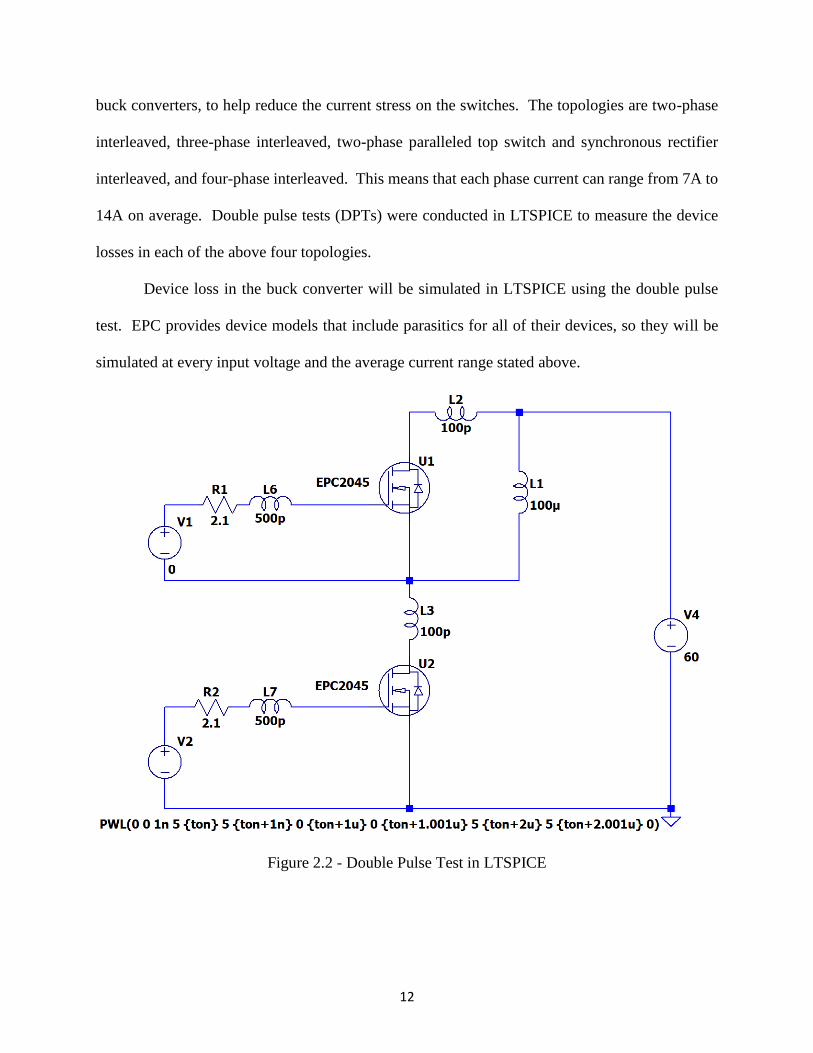
Figure 2.2 - Double Pulse Test in LTSPICE

13
Fig. 2.2 shows the DPT in LTSPICE using EPC GaN devices. This is a standard half bridge
setup that includes some of the parasitic inductances that would be expected in the actual converter
layout. The 2.1 ohm resistor in front of each device is an internal resistance to the selected gate
driver that will be used for each phase of the buck. At the time, the LM5113 was selected as the
gate driver from Texas Instruments, however recently they stopped manufacturing this device and
now recommend the LMG1205. Both of these devices are very similar with the only difference
being in the internal propagation delay. In terms of simulating the DPT, the inductor needs to be
large enough hold the current at the input voltage. The DPT will be run at 40 V, 48 V, and 60 V,
which are the minimum, nominal, and maximum input voltages.
To run the DPT the only parameter that needs to be changed is the pulse width. Depending
on what current is desired, everything else is constant. Using the following equation the pulse
length can be determined:
𝑑𝑡 =𝐿∗𝑑𝑖
𝑉𝐼𝑁 (1)
For instance, if the input voltage is set at 60 V, with the DPT inductor at 100 μH and the
desired current is 14 A, then the desired pulse length will be 23.33 μs. Fig. 2.3 shows the gate
signal for the device under test and the inductor current for which the losses will be measured for
the device. The first pulse is used to charge the inductor to the correct amount of current, while
the second pulse is used for measuring turn on and turn off losses for the device. When the first
pulse turns off, the current is relatively flat before the next pulse, so the current at the end of the
first pulse will be used to measure the turn off loss and the current at the beginning of the second
pulse will be used to measure the turn on loss.
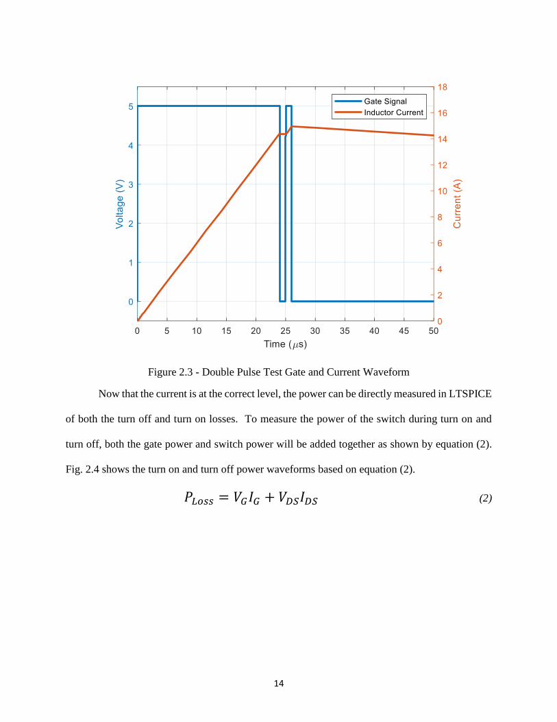
14
Figure 2.3 - Double Pulse Test Gate and Current Waveform
Now that the current is at the correct level, the power can be directly measured in LTSPICE
of both the turn off and turn on losses. To measure the power of the switch during turn on and
turn off, both the gate power and switch power will be added together as shown by equation (2).
Fig. 2.4 shows the turn on and turn off power waveforms based on equation (2).
𝑃𝐿𝑜𝑠𝑠 = 𝑉𝐺𝐼𝐺 + 𝑉𝐷𝑆𝐼𝐷𝑆 (2)

15
Figure 2.4 - Turn On and Turn Off Power
In Fig. 2.4, the ringing can be attributed to the parasitic inductance both in the circuit, which
is caused by layout, and the parasitic inductance from the package, which is included in the model
provided by EPC. The power waveforms provide some information, but in order to make it useful,
the energy is needed. Energy is the power divided by time, so in order to gather the energy; the
integral of the power needs to be taken. LTSPICE provides an integrate function on their plots, so
whatever time frame is displayed it will give the value of the integrated waveform displayed. Fig.
2.5 shows the corresponding energy to both of the turn off and turn on waveforms in Fig. 2.4.
Figure 2.5 - Turn Off Energy and Turn On Energy
Fig. 2.5 shows the turn off and turn on energy from Fig. 2.4 respectively. The turn off loss
is lower than the turn on loss because of the parasitic capacitances in the GaNFET. Based on turn

16
on and turn off energies from [9], they are impacted by the CISS and QGD from the GaNFET. From
the results, to find the power loss at a certain frequency, the energy is multiplied by the switching
frequency, which gives the resulting power loss on the device as shown by equation (3).
𝑃𝐿𝑜𝑠𝑠 = 𝐸𝑂𝑁/𝑂𝐹𝐹 ∗ 𝐹𝑆𝑊 (3)
After gathering multiple turn on and turn off energies from LTSPICE over a wide current
range, all of the points can be plotted and a line of best fit can be used for calculating loss over all
ranges much easier. For every device listed in Fig. 2.1, the turn on and turn off energy was
calculated in LTSPICE for both a single device and parallel devices.
Figure 2.6 - Turn On Energy Comparison between Devices
0
0.5
1
1.5
2
2.5
3
0 5 10 15
En
erg
y (μ
J)
Current (A)
Turn On Energy Comparison 48 V
EPC2007C
EPC2016C
EPC2045
EPC2001C
EPC2104
EPC2032
17
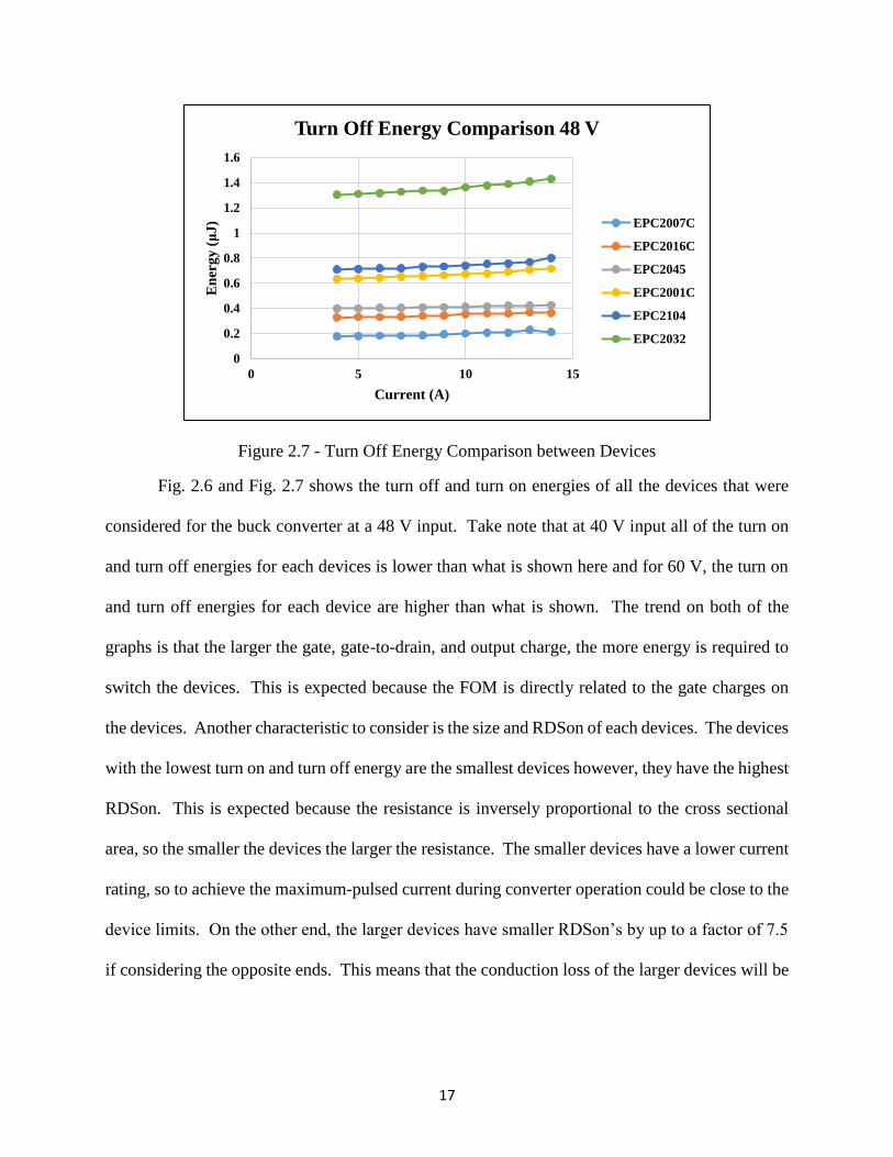
Figure 2.7 - Turn Off Energy Comparison between Devices
Fig. 2.6 and Fig. 2.7 shows the turn off and turn on energies of all the devices that were
considered for the buck converter at a 48 V input. Take note that at 40 V input all of the turn on
and turn off energies for each devices is lower than what is shown here and for 60 V, the turn on
and turn off energies for each device are higher than what is shown. The trend on both of the
graphs is that the larger the gate, gate-to-drain, and output charge, the more energy is required to
switch the devices. This is expected because the FOM is directly related to the gate charges on
the devices. Another characteristic to consider is the size and RDSon of each devices. The devices
with the lowest turn on and turn off energy are the smallest devices however, they have the highest
RDSon. This is expected because the resistance is inversely proportional to the cross sectional
area, so the smaller the devices the larger the resistance. The smaller devices have a lower current
rating, so to achieve the maximum-pulsed current during converter operation could be close to the
device limits. On the other end, the larger devices have smaller RDSon’s by up to a factor of 7.5
if considering the opposite ends. This means that the conduction loss of the larger devices will be
0
0.2
0.4
0.6
0.8
1
1.2
1.4
1.6
0 5 10 15
En
erg
y (μ
J)
Current (A)
Turn Off Energy Comparison 48 V
EPC2007C
EPC2016C
EPC2045
EPC2001C
EPC2104
EPC2032

18
small based on I2R, but they will have larger switching losses. There is a tradeoff between size
and loss, which can be calculated and the best candidate can be chosen.
Since this is a traditional buck converter, the equations for every loss, current, and voltage
in the converter are already known. With a given inductance, the peak-to-peak current can be
calculated and from that, the switching and conduction losses can be compared over the full power
range. The following equations are used to calculate the losses in the buck converter:
𝛥𝑖𝐿 = (𝑉𝑖𝑛−𝑉𝑜𝑢𝑡)∗
𝑉𝑜𝑢𝑡𝑉𝑖𝑛
𝑓𝑠∗𝐿 (4)
𝐼𝑜 = 𝑃𝑜
𝑉𝑜 (5)
𝑇𝑢𝑟𝑛 𝑂𝑛 𝑐𝑢𝑟𝑟𝑒𝑛𝑡 = 𝐼𝑜 −𝛥𝑖𝐿
2 (6)
𝑇𝑢𝑟𝑛 𝑂𝑓𝑓 𝑐𝑢𝑟𝑟𝑒𝑛𝑡 = 𝐼𝑜 +𝛥𝑖𝐿
2 (7)
𝐼𝑅𝑀𝑆 = √𝐼𝑜2 +
𝛥𝑖𝐿2
12 (8)
𝐷𝑟𝑖𝑣𝑖𝑛𝑔 𝐿𝑜𝑠𝑠 = (𝑄𝐺𝐻 + 𝑄𝐺𝐿) ∗ 𝑉𝐷𝐷2 ∗ 𝑓𝑠 (9)
𝐶𝑜𝑛𝑑𝑢𝑐𝑡𝑖𝑜𝑛 𝐿𝑜𝑠𝑠 𝑇𝑜𝑝 𝐷𝑒𝑣𝑖𝑐𝑒 = 𝐼𝑅𝑀𝑆2 ∗ 𝑅𝐷𝑆𝑜𝑛 ∗ (
𝑉𝑜𝑢𝑡
𝑉𝑖𝑛) (10)

19
𝐶𝑜𝑛𝑑𝑢𝑐𝑡𝑖𝑜𝑛 𝐿𝑜𝑠𝑠 𝑆𝑅 = 𝐼𝑅𝑀𝑆2 ∗ 𝑅𝐷𝑆𝑜𝑛 ∗ (1 −
𝑉𝑜𝑢𝑡
𝑉𝑖𝑛) (11)
Equations (4) through (11) are used to calculate the losses in the buck converter excluding
the inductor losses. Since, the inductor is designed later in the process, the inductance was kept
constant for every single device and the series resistance of the inductor was not considered. The
inductance was set at 11 μH for all cases. The loss comparison was calculated at 40V, 48V, and
60V, however when the comparison is made, only 48V is considered because when the voltage
increase and decreases, the loss follows, it is either higher or lower. Another note is that all of the
RDSon’s from Fig. 2.1 are multiplied by 1.5 in order to compensate for the rise in RDSon when
the temperature increases. Even though the final temperature of the devices is unknown taking the
absolute maximum temperature as 110 °C corresponds to a 1.5 multiplier on the normal RDSon.
All of these equations are standard for a buck converter except for equation (9). Equation (9) is
given by the datasheet for the LMG1205, which is a special gate driver that is used to drive GaN
devices. It prevents the gate signal from going above 5V and damaging the GaN device.
In order to choose the best device for the application, an efficiency curve was used to
determine which device would provide the larges efficiency over all topologies. Using the data
from Fig. 2.6 and Fig. 2.7, a line of best fit could be placed for each device turn on and turn off
energy. This line was made for both single devices and paralleled devices. With fitted line,
equation (3) can then be used to calculate the total switching power loss in the buck converter. To
find the turn on power, equation (6) is used to calculate the current and then that current is used
with fitted line to find the energy, and finally equation (3) is used to calculate the power. The same
process is used for the turn off power.
To account for all of the losses, the turn on of device one, turn off one, conduction loss for
device one and device 2, and the driving loss for both devices one and two are summed up and the
20
efficiency is calculated. Note that there are no switching losses on the synchronous rectifier (SR)
because it is being used as a diode, there is no switching when current is running through the
device. The only loss on the SR is the conduction loss and driving loss. To get the efficiency
curve, the power is stepped from 25W (depending on how many phases are being used) to 1000W,
when the power changed the output current changes and so do the switching and conduction losses.
All of the figures shown were run at 500 kHz switching frequency. The following figures compare
how efficient each device is over the entire power range.
Figure 2.8 - Two-Phase Efficiency Device Comparison
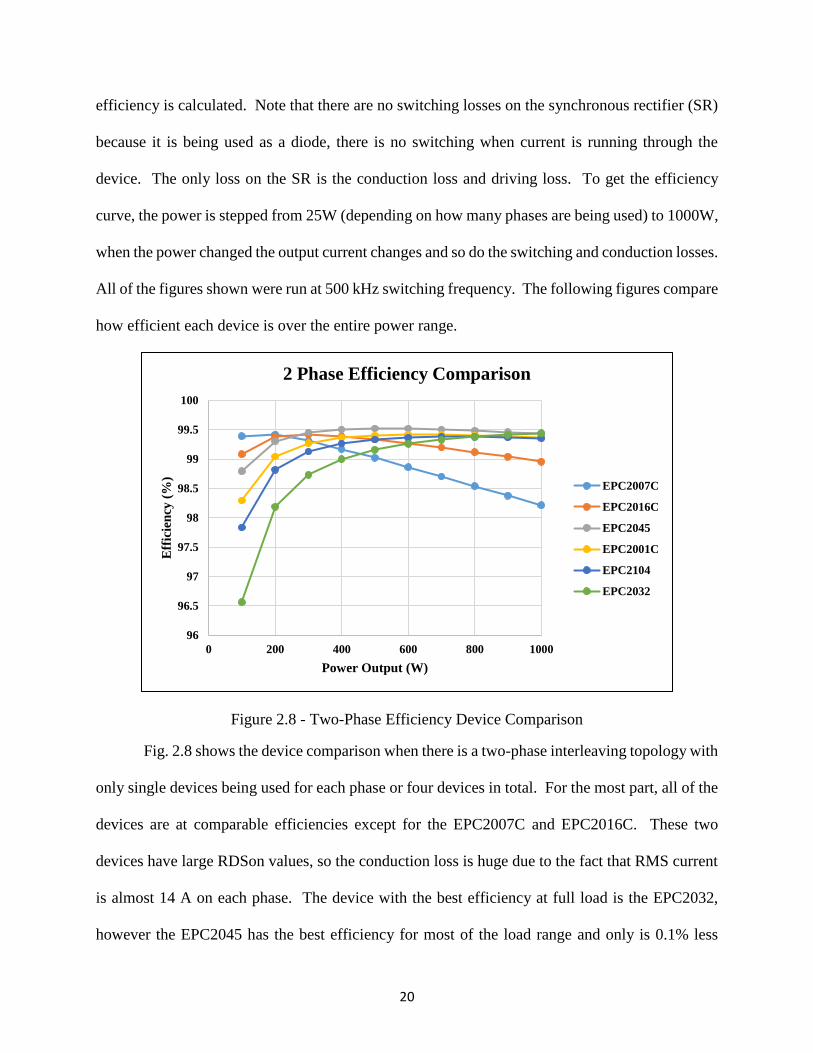
Fig. 2.8 shows the device comparison when there is a two-phase interleaving topology with
only single devices being used for each phase or four devices in total. For the most part, all of the
devices are at comparable efficiencies except for the EPC2007C and EPC2016C. These two
devices have large RDSon values, so the conduction loss is huge due to the fact that RMS current
is almost 14 A on each phase. The device with the best efficiency at full load is the EPC2032,
however the EPC2045 has the best efficiency for most of the load range and only is 0.1% less
96
96.5
97
97.5
98
98.5
99
99.5
100
0 200 400 600 800 1000
Eff
icie
ncy
(%
)
Power Output (W)
2 Phase Efficiency Comparison
EPC2007C
EPC2016C
EPC2045
EPC2001C
EPC2104
EPC2032

21
efficient than the EPC2032 at full load. For the two-phase interleaving topology, the EPC2045
was decided as the best device to use in this case.
Figure 2.9 - Three-Phase Efficiency Device Comparison
Fig. 2.9 shows the device comparison when there is a three-phase interleaving topology
with only single devices being used with six devices in total. The efficiencies in this graph start
to move closer together, however the same trend follows. The EPC2032 starts to lose efficiency
because the switching loss starts to dominate, which is expected because QG is very large.
However, once again, the EPC2045 has the highest efficiency over most of the load range and has
the highest efficiency at full load. The EPC2045 was chosen as the device for the three-phase
interleaving topology.
94.5
95
95.5
96
96.5
97
97.5
98
98.5
99
99.5
100
0 200 400 600 800 1000
Eff
icie
ncy
(%
)
Power Output (W)
3 Phase Efficiency Comparison
EPC2007C
EPC2016C
EPC2045
EPC2001C
EPC2104
EPC2032
22
Figure 2.10 - Four-Phase Efficiency Device Comparison
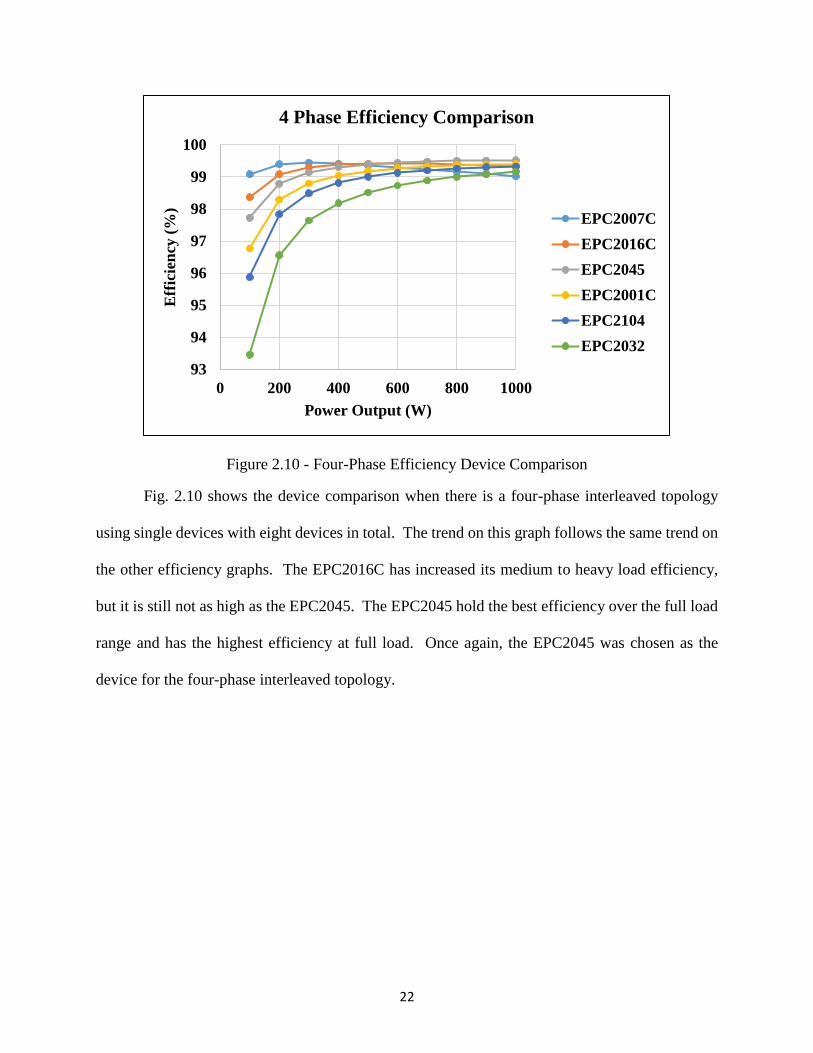
Fig. 2.10 shows the device comparison when there is a four-phase interleaved topology
using single devices with eight devices in total. The trend on this graph follows the same trend on
the other efficiency graphs. The EPC2016C has increased its medium to heavy load efficiency,
but it is still not as high as the EPC2045. The EPC2045 hold the best efficiency over the full load
range and has the highest efficiency at full load. Once again, the EPC2045 was chosen as the
device for the four-phase interleaved topology.
93
94
95
96
97
98
99
100
0 200 400 600 800 1000
Eff
icie
ncy
(%
)
Power Output (W)
4 Phase Efficiency Comparison
EPC2007C
EPC2016C
EPC2045
EPC2001C
EPC2104
EPC2032
23
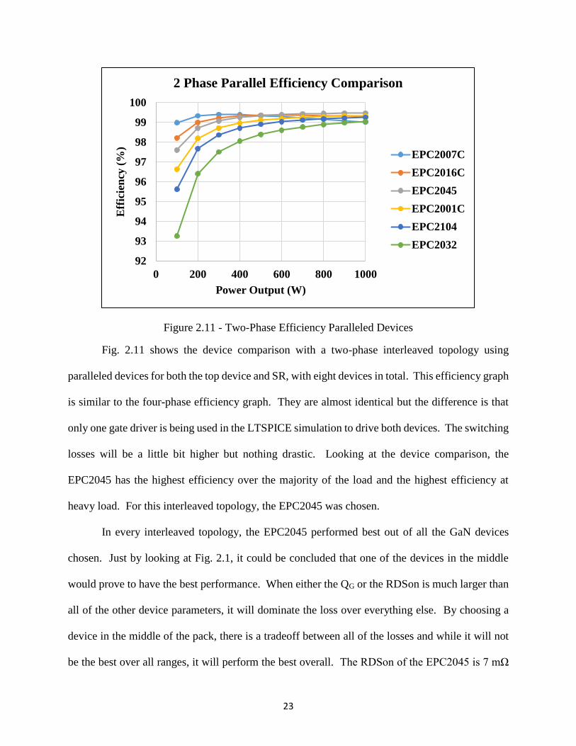
Figure 2.11 - Two-Phase Efficiency Paralleled Devices
Fig. 2.11 shows the device comparison with a two-phase interleaved topology using
paralleled devices for both the top device and SR, with eight devices in total. This efficiency graph
is similar to the four-phase efficiency graph. They are almost identical but the difference is that
only one gate driver is being used in the LTSPICE simulation to drive both devices. The switching
losses will be a little bit higher but nothing drastic. Looking at the device comparison, the
EPC2045 has the highest efficiency over the majority of the load and the highest efficiency at
heavy load. For this interleaved topology, the EPC2045 was chosen.
In every interleaved topology, the EPC2045 performed best out of all the GaN devices
chosen. Just by looking at Fig. 2.1, it could be concluded that one of the devices in the middle
would prove to have the best performance. When either the QG or the RDSon is much larger than
all of the other device parameters, it will dominate the loss over everything else. By choosing a
device in the middle of the pack, there is a tradeoff between all of the losses and while it will not
be the best over all ranges, it will perform the best overall. The RDSon of the EPC2045 is 7 mΩ
92
93
94
95
96
97
98
99
100
0 200 400 600 800 1000
Eff
icie
ncy
(%
)
Power Output (W)
2 Phase Parallel Efficiency Comparison
EPC2007C
EPC2016C
EPC2045
EPC2001C
EPC2104
EPC2032
24
and the QG is 5.2 nC. By also doing a rough FOM calculation, the product of these two values is
lower than all of the other FOM from the other devices. Since the EPC2045 was chosen as the
device for the buck converter, the topologies can now be compared.
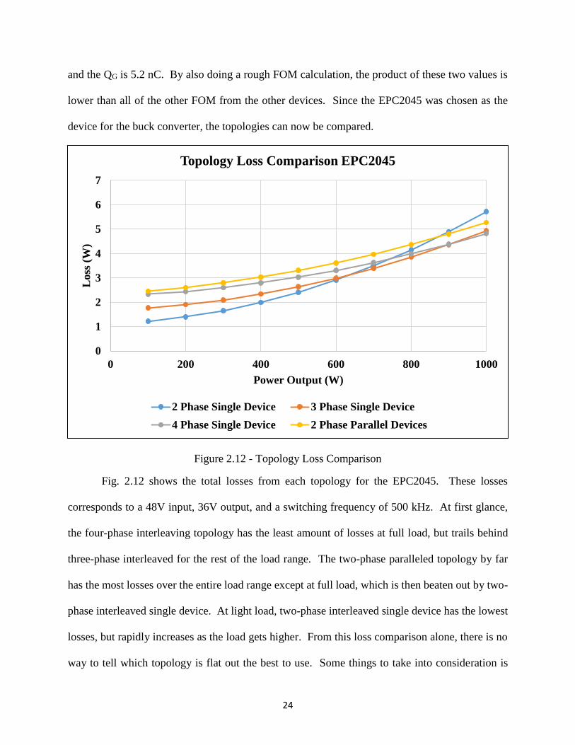
Figure 2.12 - Topology Loss Comparison
Fig. 2.12 shows the total losses from each topology for the EPC2045. These losses
corresponds to a 48V input, 36V output, and a switching frequency of 500 kHz. At first glance,
the four-phase interleaving topology has the least amount of losses at full load, but trails behind
three-phase interleaved for the rest of the load range. The two-phase paralleled topology by far
has the most losses over the entire load range except at full load, which is then beaten out by two-
phase interleaved single device. At light load, two-phase interleaved single device has the lowest
losses, but rapidly increases as the load gets higher. From this loss comparison alone, there is no
way to tell which topology is flat out the best to use. Some things to take into consideration is
0
1
2
3
4
5
6
7
0 200 400 600 800 1000
Loss
(W
)
Power Output (W)
Topology Loss Comparison EPC2045
2 Phase Single Device 3 Phase Single Device
4 Phase Single Device 2 Phase Parallel Devices

25
board size. The board needs to fit anywhere from four to eight devices plus gate drivers. If only
four devices are being used for the two-phase, then there will be 14 A on average of current running
through the inductor, so the inductor will need to be larger, but will it fit in with defined board
limits. On the other end, if four-phase interleaved topology is used, the current will be smaller but
there needs to be four inductors or it would need to be a coupled inductor. In addition, the
switching frequency needs to be chosen, which will impact both the switching losses and inductor
size. The higher the switching frequency, the more switching losses, but the smaller the inductor.
The only decision made was to use the EPC2045 as the device of choice for both the top
device and SR for all topologies. In the coming sections, the benefits and drawback of each
topology will be discussed in detail as well as selecting the switching frequency.
2.3 Electro-Thermal Design
The next step in the design of the buck converter was to test the thermal performance of
the EPC2045. From the project specifications, the converter was to run in a 55 °C environment,
so thermal management of the converter is important. EPC devices have an operating temperature
between -40 °C and 150 °C. This means that with the ambient temperature of 55 °C, the operation
temperature of the buck converter should be kept below 100 °C with conventional cooling. The
scope of this project did not include designing a heat sink for either part of the converter, so it will
be assumed that only conventional cooling or cooling with a fan will be used. There is also no
access to a thermal chamber, so all testing is done at room temperature and the analysis will be
done at room temperature.
In order to test the thermal performance of the EPC2045, an actual PCB would need to be
fabricated. EPC provides a demo/development board that includes a half bridge topology using
the EPC2045 as both the top device and SR. Using one of the development boards from EPC, a
26
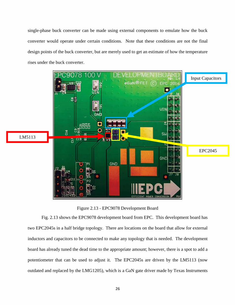
Input Capacitors
EPC2045
LM5113
single-phase buck converter can be made using external components to emulate how the buck
converter would operate under certain conditions. Note that these conditions are not the final
design points of the buck converter, but are merely used to get an estimate of how the temperature
rises under the buck converter.
Figure 2.13 - EPC9078 Development Board
Fig. 2.13 shows the EPC9078 development board from EPC. This development board has
two EPC2045s in a half bridge topology. There are locations on the board that allow for external
inductors and capacitors to be connected to make any topology that is needed. The development
board has already tuned the dead time to the appropriate amount; however, there is a spot to add a
potentiometer that can be used to adjust it. The EPC2045s are driven by the LM5113 (now
outdated and replaced by the LMG1205), which is a GaN gate driver made by Texas Instruments
27
(TI), which will prevent overshoot on the gate of the GaN. There is also a location to change the
gate resistor for turn on and turn off if needed. The main components of the development board
are highlighted.
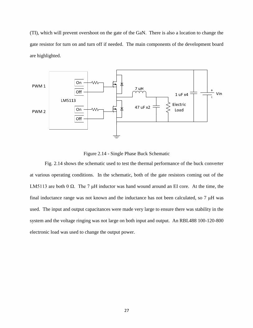
Figure 2.14 - Single Phase Buck Schematic
Fig. 2.14 shows the schematic used to test the thermal performance of the buck converter
at various operating conditions. In the schematic, both of the gate resistors coming out of the
LM5113 are both 0 Ω. The 7 μH inductor was hand wound around an EI core. At the time, the
final inductance range was not known and the inductance has not been calculated, so 7 μH was
used. The input and output capacitances were made very large to ensure there was stability in the
system and the voltage ringing was not large on both input and output. An RBL488 100-120-800
electronic load was used to change the output power.
28
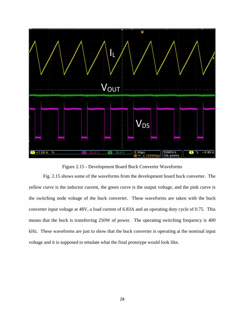
Figure 2.15 - Development Board Buck Converter Waveforms
Fig. 2.15 shows some of the waveforms from the development board buck converter. The
yellow curve is the inductor current, the green curve is the output voltage, and the pink curve is
the switching node voltage of the buck converter. These waveforms are taken with the buck
converter input voltage at 48V, a load current of 6.83A and an operating duty cycle of 0.75. This
means that the buck is transferring 250W of power. The operating switching frequency is 400
kHz. These waveforms are just to show that the buck converter is operating at the nominal input
voltage and it is supposed to emulate what the final prototype would look like.
IL
VOUT
VDS

29
Figure 2.16 - Thermal Image of Development Board
Fig. 2.16 shows a thermal image of the buck converter operating under the conditions
shows in Fig. 2.15. The hottest part of the thermal image is the top side device in the buck
converter. This is expected because the top side device not only has conduction loss, but it also
includes the switching losses. The maximum temperature achieved in steady state from the device
was 63.7 °C. There was no cooling put on this board, it was just sitting at room temperature and
allowed to heat up. Using this the temperature information, multiple points can be plotted on a
curve to see how the temperature changes versus the calculated device loss from the previous
section. Since the temperature reading is only of the top side device, only the losses on the top
side device are used to plot.

30
Figure 2.17 - Device Loss vs Temperature
Fig. 2.17 shows the device loss of the top device versus the temperature of the case. These
temperatures were taken with conventional cooling meaning the board was sitting at room
temperature. Each set of three points represents the switching frequency changing from 200 kHz
to 300 kHz to 400 kHz. The points on the left side are when the power of the buck is at 125W and
the points on the right are when the power of the buck is at 250W. The 23.984 represents the room
temperature and the 69.213 represents the thermal resistance from case to ambient. There is no
comparison to case to ambient thermal resistance, but the datasheet provides the junction to
ambient which is typically 64 °C/W. This is fairly close to the value calculated from the
experiment, so it should be a good indicator of device temperature in the final prototype design.
The benefit of this plot is that the switching frequency can be swept over a variety of ranges and
the loss can be calculated and then using the line of best fit, a temperature can be estimated.
Knowing the device loss, one can find the approximate temperature of the case of the device. This
helps in knowing how much loss is acceptable on the top side device while keeping in mind the
project ambient temperature requirements.
y = 69.213x + 23.984
0
10
20
30
40
50
60
70
0.2 0.3 0.4 0.5 0.6
Tem
per
atu
re (°C
)
Q1 Device Loss (W)
Device Loss vs Case Temperature

31
Since the datasheet for the device recommends the safe operating temperature to not exceed
150 °C and the project requirements have the ambient temperature set to 50 °C, the maximum
device temperature should not exceed 100 °C. Using the line of best fit from Fig. 2.17, the
maximum allowable device loss on the top device should be limited to 1.1 W. Using the equations
that calculated the best device for this application, one can use the same equations to find the
device loss on the top side device and sweep the frequency to see how high one can achieve.
Table 2.1 - Top Device Loss Topology vs Frequency
Buck
Topology
Loss @ 200
kHz
Loss @ 300
kHz
Loss @ 400
kHz
Loss @ 500
kHz
Loss @ 600
kHz
2 Phase
Single
Device
1.84355 W 2.00109 W 2.1626 W 2.3256 W 2.48837 W
3 Phase
Single
Device
0.96349 W 1.10298 W 1.24644 W 1.39104 W 1.53609 W
4 Phase
Single
Device
0.65006 W 0.78052 W 0.91945 W 1.05052 W 1.18655 W
2 Phase
Paralleled
Devices
0.68946 W 0.84719 W 1.00591 W 1.1649 W 1.32405 W
Table 2.1 shows the loss breakdown for the top device versus the topology and switching
frequency. In the two-phase single device topology, the maximum power that runs through each
phase is 500W, so the top device loss is shown at 500W. For the three-phase single device, the
maximum power per phase is 333.33W. For the four-phase single device, the maximum power
per phase is 250W. For the two-phase paralleled devices, the maximum power per phase is 500W,
but if one assumes perfect current sharing among devices, the maximum power per device is
250W.

32
2.4 Topology Evaluation
The two-phase single device topology does not meet the minimum loss requirement for the
first device. Even running the converter at 200 kHz would put the estimated device temperature
at 150 °C, so that topology can be ruled out. The three-phase single device topology works for
only 200 kHz and 300 kHz, which is fine however, the magnetics would be larger than if another
topology was to be selected. The four-phase interleaved topology can work up to 500 kHz and
even if the temperature was pushed a little higher, then even 600 kHz would be possible to keep
the devices under 100 °C. Lastly, the two-phase interleaved with paralleled devices works up to
400 kHz and possible even 500 kHz if some leeway was allowed.
To summarize the results, two-phase single device topology was not considered. Three-
phase interleaved topology, is an option, however one would need to fit three inductors into a small
area or come up with a novel three-phase coupled inductor. While the three-phase coupled
inductor could work, due to the time constraint on the project only a certain amount of time could
be dedicated to magnetic design, so this topology will not be investigated further. The four-phase
interleaved topology works up to 500 kHz and shows to have the lowest loss at full load. The only
challenged will be to design the magnetics with either four separate inductors, two separate
coupled inductors, or one large four-phase coupled inductors. This topology will be investigated
further for the multi-phase buck converter. The two-phase interleaved topology with paralleled
devices can work up to 400 kHz and possibly 500 kHz, however the only drawback will be to fit
an inductor large enough to handle and average current of 14A per phase. A possible solution is
to use one coupled inductor or two separate inductors for the magnetics. This topology will also
be investigate further.
33
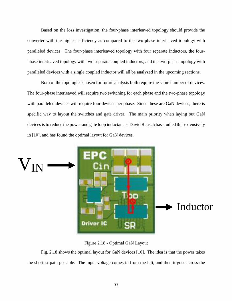
VIN
Inductor
Based on the loss investigation, the four-phase interleaved topology should provide the
converter with the highest efficiency as compared to the two-phase interleaved topology with
paralleled devices. The four-phase interleaved topology with four separate inductors, the four-
phase interleaved topology with two separate coupled inductors, and the two-phase topology with
paralleled devices with a single coupled inductor will all be analyzed in the upcoming sections.
Both of the topologies chosen for future analysis both require the same number of devices.
The four-phase interleaved will require two switching for each phase and the two-phase topology
with paralleled devices will require four devices per phase. Since these are GaN devices, there is
specific way to layout the switches and gate driver. The main priority when laying out GaN
devices is to reduce the power and gate loop inductance. David Reusch has studied this extensively
in [10], and has found the optimal layout for GaN devices.
Figure 2.18 - Optimal GaN Layout
Fig. 2.18 shows the optimal layout for GaN devices [10]. The idea is that the power takes
the shortest path possible. The input voltage comes in from the left, and then it goes across the

34
input capacitors and across the top device and synchronous rectifier. The power path then goes
down one layer and returns straight back to the ground at the input capacitors as shown in Fig.
2.19.
Figure 2.19 - Optimal Power Loop for GaN Devices
Using the information provided by EPC and this paper, a preliminary layout can be
constructed to see how much room would be needed for the power stage and the inductor for the
four-phase interleaved topology.
Figure 2.20 - Preliminary Four-Phase Interleaved Topology

35
Fig. 2.20 shows what a preliminary layout would look like if the four-phase interleaved
topology was used. Shown on the layout is the LMG1205 gate driver, with two EPC2045 per
phase, with input capacitors, a high side gate resistor, the bootstrap and VDD capacitor. Referring
back to section 2.1, the initial size of the buck converter was set at 30mm x 35mm x 7mm. Using
Altium software, the switches and gate driver can be measured to see how much space is used.
The initial layout of the GaN devices takes approximately 7.1 mm of space, so this leaves around
22 mm for the depth of the inductor and 35 mm for the width of the inductor. The benefit to this
layout is that each phase is identical to each other, so the layout is relatively easily once one phase
is completed.
The major concern with paralleling any switch is that the current might not distribute
evenly between paralleled devices. This is caused by large inductance in the power and gate loop
as well as non-symmetrical loops. If there are many devices being paralleled and only one gate
driver is used to drive all of them, then there is a great possibility that the gate signal for one of the
switching is different from the others, which leads to different turn on for all the switches. If all
of the devices turn on at different times, then there will be current imbalance between all devices
as described by [11].
However, in the case of two-phase topology with paralleled devices, there will only be two
devices paralleled. Using Fig. 2.20, two of the gate drivers can be removed and the capacitors can
be moved around to make the layout more symmetrical for the paralleled layout.

36
Figure 2.21 - Two-Phase Topology with Paralleled Devices Preliminary Layout
Fig. 2.21 shows the preliminary layout for the two-phase topology with paralleled devices.
There is not much difference between this layout and the layout for the four-phase interleaved
topology. The inductor will still have the same room whether it is decided to use a coupled
inductor or two separate inductors. Once again, there will be 22 mm x 35 mm for the inductor(s).
However, the one concern is that there is now double the current running though the inductor in
the same amount of space for the paralleling case. This leads to high di/dt and it could possibly
saturate the core in the allotted space. However, this will all be discussed in the next chapter.
In summary, the four-phase topology and two-phase topology with paralleled devices will
be further investigated in the magnetics design. Each topology will have 22mm x 35 mm x 7 mm
to fit the magnetics and need to ensure the core will not saturate. Each magnetic design will also
need to consider the way in which the power flows from the buck to the LLC.

37
Chapter 3. Planar Magnetics Design
3.1 Magnetics Structure and Background
The magnetics for both the buck converter and LLC will utilize planar magnetics in order
to help save space. With the increase in switching frequency, it will allow the magnetics to be
smaller and use the PCB for the windings. The only parameter that the buck and LLC share is the
number of layers on the PCB. If one uses 10 layers then the other will have to use 10 layers.
In traditional IBCs, most of the converters use up to 14 layers on their printed circuit board.
The relationship between layer number and efficiency is directly proportional to each other. The
more layers that are on the PCB, the higher the efficiency and the lower amount of layers, the
lower the efficiency. The reason is related to the series resistance with the planar magnetic
component being designed. The resistance of a 3-dimensional (3D) object varies with the length
and area of the conductor as shown by equation (12).
𝑅𝑒𝑠𝑖𝑠𝑡𝑎𝑛𝑐𝑒 = 𝜌∗𝐿
𝐴 (12)
In planar magnetics, multiple layers are used for one turn of the transformer or the inductor.
Assuming that copper is used for each of the layers in the PCB, ρ will be constant. If there are
more conductors, then the cross sectional area increases, while the length stays the same because
the layers will be paralleled. If the area increases in a conductor then the overall resistance will
decrease.
Another variable in the resistance equation is the thickness of the layers. The thickness
contributes to the cross sectional area, however it is not that straight forward. The buck converter
current is mostly DC current with a small AC ripple, so skinning effect will not impact the series
resistance of the inductor on the buck. However, in the LLC, a transformer is used, so the current

38
is AC and the skin effect contributes to a large part of the losses. Standard PCBs use 1 oz. (34.7
μm) copper for the thickness of the layers. However, when higher currents are transferred, 1 oz.
copper is not the most optimal. The thickness needs to be increased to see which thickness gives
the lowest losses. It was not the scope of the buck to determine this; however, the student in charge
of the LLC determined that the resonant and switching frequency of the LLC would be 1 MHz.
After simulating and testing other converters at this switching frequency, 2 oz. copper proved to
produce the lowest loss at 1 MHz. The entire PCB uses 2 oz. copper for the thickness of the layers.
As stated earlier, 14 layers is the maximum layer count of most IBCs, so there is no reason to
sacrifice efficiency for minimal gains in power density. FR4 is used as the insulation between the
internal layers on the board and the thickness was determined to be 0.105 mm. With the layer
count, layer thickness, and insulation thickness known, the final board thickness will be 2.37 mm
thick.
The first step in designing the inductor for the buck converter is to choose a magnetic
material that will be suitable at the operating frequency. From the previous chapter, the highest
operating frequency that was under consideration was 500 kHz for the four-phase interleaved. At
the request of Lockheed Martin, 1 MHz materials were also researched. The goal of the converter
was to showcase pushing the switching frequency of GaN devices, so higher frequency materials
were considered for the magnetics.

39
Figure 3.1 - Magnetic Materials for Inductor
Fig. 3.1 shows the magnetic materials that were considered for the buck converter inductor.
Magnetics from larger manufacturers were considered in order to ensure the manufacturability and
the lead-time of the cores. Ferroxcube had both 500 kHz materials and 1 MHz materials. Of the
ones displayed they provided the best performance. The biggest factors to consider here are the μi
and the saturation. The larger the permeability, the larger the inductance can be in the same amount
of area. The larger the saturation of the material, the core can shrunk to a smaller size, which in
turn raises the B-field in the core. However, even though the saturation is posted here, that value
will not be used as the absolute maximum, a smaller value in the linear region of the BH curve is
considered. In terms of the 500 kHz material, 3F36 provides a higher permeability, so it is chosen
as the material of choice for 500 kHz. None of the 1 MHz materials were considered for this
experiment due to the high switching frequency. From chapter two, if the devices were to be hard
switched at 1 MHz, the device temperature would be around 150 °C at room temperature, which
would not meet the specifications of the project. The magnetic material that was used for the LLC

40
was ML91S from Hitachi Metals. It has been used before and it has very low core loss at 50 mT.
If a material was to be chosen for 1 MHz two-phase topology with paralleled devices, ML91S
would be the material.
Two different magnetic structures were investigated further for the four-phase interleaved
topology: two coupled inductors and four separate inductors. The first case that will be discussed
is the two separate coupled inductors for the magnetics. In order for an inductor to be coupled,
each phase inductor will need to share a common core with each other. Based on the size allotted
for the magnetics, two different structures were considered, a UI core and an EI core.
The major difference between each of the cores is that the EI core has a center post and the
UI core does not. The benefit of having an extra post in the EI core is that one can control the
coupling between both phase inductors. In a UI core, however the phase inductors are defined;
the coupling will be set in place and cannot be changed unless the each phase inductance can be
changed. The drawback for the extra post in the EI core is that there is slightly more core loss
because there is extra magnetic material. When designing a coupled inductor, one of the main
benefits is that, the current ripple can be reduced during the steady state, while keeping the transient
inductance lower than the steady state. In order to keep the steady state inductance higher than the
transient, the coupling coefficient needs to satisfy certain inequalities, which will be discussed
later [12]. With a UI core, there is no way to control the coupling without redesigning the entire
inductor, so optimization is difficult when all of the parameters change without having a control
variable. The goal of this project was to optimize the lowest possible loss with the highest power
density, so in the end, the core shape for the inductor was chosen to be an EI core.
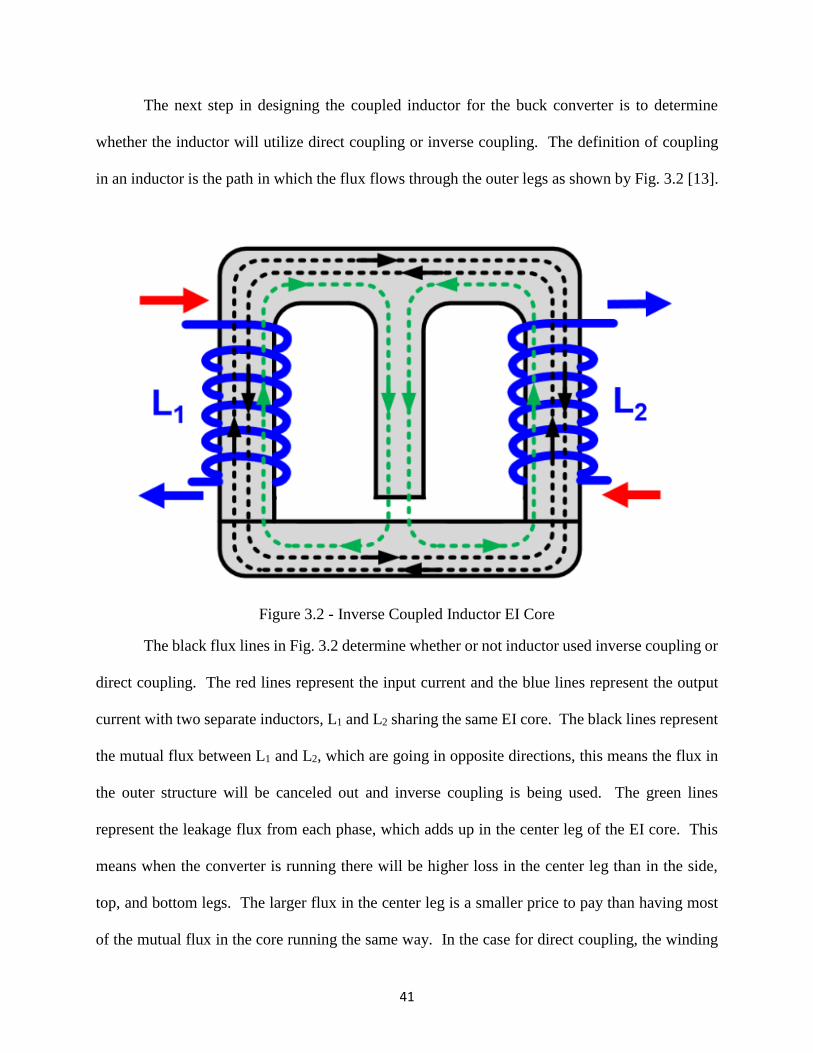
41
The next step in designing the coupled inductor for the buck converter is to determine
whether the inductor will utilize direct coupling or inverse coupling. The definition of coupling
in an inductor is the path in which the flux flows through the outer legs as shown by Fig. 3.2 [13].
Figure 3.2 - Inverse Coupled Inductor EI Core
The black flux lines in Fig. 3.2 determine whether or not inductor used inverse coupling or
direct coupling. The red lines represent the input current and the blue lines represent the output
current with two separate inductors, L1 and L2 sharing the same EI core. The black lines represent
the mutual flux between L1 and L2, which are going in opposite directions, this means the flux in
the outer structure will be canceled out and inverse coupling is being used. The green lines
represent the leakage flux from each phase, which adds up in the center leg of the EI core. This
means when the converter is running there will be higher loss in the center leg than in the side,
top, and bottom legs. The larger flux in the center leg is a smaller price to pay than having most
of the mutual flux in the core running the same way. In the case for direct coupling, the winding

42
would be in the opposite direction and the mutual flux would be in the same direction for the side,
top, and bottom part of the core. However, the leakage flux would be canceled out in the center
leg.
Another comparison between direct and inverse coupled inductors is the difference in the
peak-to-peak steady state currents. The buck converter operates nominally at 48V, but can also
operate at 40V and 60V input. With a 36V output, this means that the minimum to maximum duty
cycle for the buck converter would range from 0.6 to 0.9. This plays an important role in
determining whether or not to directly couple or inversely couple the inductors.
Figure 3.3 - Direct Coupling versus Inverse Coupling
Fig. 3.3 shows the current waveform when the inductors are coupled together. The solid
line represent the current when the inductors are coupled and the dashed line represent the current
when the inductors are not coupled. When an inductor is coupled, the inductance changes to three
different values during normal operation [12]. The peak-to-peak current is determined by LEQ3 in
each case, in terms of direct coupling, the inductance of LEQ3 is smaller than the inductance when
the there is no coupling. In comparison, the inductance of LEQ3 for inverse coupling is larger than

43
the steady state inductance when the inductors are not coupled. This means that when using
inverse coupled inductors, the steady state current can be lower than that of non-coupling
inductors. Take note that this is only valid in some cases, from [12] if the following inequality is
not satisfied, then the steady state peak-to-peak current ripple of a coupled inductor will be larger
than a non-coupled inductor.
−𝛼 < 𝐷′
𝐷 (13)
Equation (13) states that the coupling coefficient (α) needs to be smaller than ratio of the
off time to one time of the buck converter. Note that the coupling coefficient is negative for inverse
coupled inductors, so the equation makes it positive so the comparison makes sense. In the case
for the buck converter being designed, in order for this inequality to be satisfied, the coupling
would have to be smaller than 0.111, and would have to be smaller than 0.333 if it was to work
under nominal operating conditions. This is both a benefit and a drawback because in addition to
increasing the steady state inductance, coupled inductors can also reduce the transient inductance
making the converter respond faster when the load changes. Equations (14) through (16) describe
the waveforms depicted in Fig. 3.3 for the inverse coupling case:
𝐿𝐸𝑄1 = (1−𝛼2)
1+𝐷
𝐷′𝛼∗ 𝐿 (14)
𝐿𝐸𝑄2 = 𝐿 ∗ (1 + 𝛼) (15)
𝐿𝐸𝑄3 = (1−𝛼2)
1+𝐷′
𝐷𝛼
∗ 𝐿 (16)
LEQ2 determines the transient inductance. Since inverse coupling is being used, LEQ2 will
always be smaller than the nominal inductance. LEQ3 is directly used to calculate the steady state
current ripple. If designed correctly, then the steady state current ripple will be smaller than if a

44
normal inductor with no coupling is used. LEQ1 is just used to calculate the remaining part of the
coupled inductor waveform. If direct coupling was being used, the coupling coefficient would be
positive making LEQ2 larger than the nominal inductance, which in turn would increase the
transient inductance, increases the response time during a load change. In terms of inverse
coupling, if the coupling coefficient is small, less than 0.1, then there is not much benefit to the
transient inductance, just to the steady state inductance. With a larger coupling coefficient, the
transient inductance can be over half the nominal inductance and it can be even four times smaller
than that if the four-phase interleaved topology is chosen. It is not guaranteed that equation (14)
can be satisfied because the coupling coefficient is very small, which either means that the overall
phase inductance will be smaller making the core smaller, which in turn will increase the B-field
in each leg, getting closer to the saturation of the material.
Figure 3.4 - Direct vs Inverse Coupling B-Field Comparison

45
Fig. 3.4 shows a simulation from ANSYS Maxwell that compares the difference between
direct and inverse coupling of the inductors. The simulation uses 3F36 as the material, with 12
layers of copper to represent the windings of the inductor. There are six turns on each inductor,
with two paralleled copper layers for each winding. The inductance is 5 μH, with the buck
converter operating at 48V and 1 kW output. The switching frequency is 300 kHz on the coupling
is 0.5 for each case. The corresponding current is input onto the windings assuming perfect current
sharing among windings and no via loss. On the left side for direct coupling, the current flows
into the page when looking at the two internal windings. This results in mutual flux adding
together on the outer edges and allows the leakage flux to cancel in the center leg. On the right
side, the current is flowing in opposite directions when looking at the two internal windings. This
allows the mutual flux to cancel out on the outer edges and the leakage flux to add together in the
center leg. By looking as the B-Field distribution one can see that direct coupling of the inductors
results in a larger B-Field distribution on the outer legs increasing almost to 820-mT at the corners,
which would surely saturate the core. In comparison, the inverse coupling only reaches 300-mT
peak B-Field at the worst point. Even though the B-field distribution is higher in inverse coupling,
the overall B-Field in the in inverse coupling is lower than that of direct coupling. The orange and
blue curves represent the B-field in the side leg, which includes the switching frequency
information from the buck converter. The center leg is double the frequency of the side legs due
to the nature of coupling the inductors between two phases. Since each phase is 180° is out of
phase, the output ripple from an interleaved buck converter will multiply the frequency of the
ripple based on how many phases are in the inductor. This is a two-phase coupled inductor, so the
frequency increases to 600 kHz in the center leg. When the full four-phase converter is put

46
together, the output current and voltage ripple will be four times that of the switching frequency
chosen.
Based on the information and simulations run, inversely coupling the inductors will benefit
the buck converter much more than directly coupling them. By inversely coupling the inductor,
lower core loss, lower transient inductance, and possibly higher steady inductance can be achieved,
which will improve the efficiency and performance of the buck converter. Direct coupling does
not provide any benefit other than cancelling the leakage flux in the center leg. Even if the center
leg was removed and a UI core was used, direct coupling would provide no benefit at all. It was
decided that inverse coupling would be used to design the coupled inductors for the buck converter.

47
3.2 Design of Inductors: Two-Phase Coupled Inductor for Four-Phase Buck
In the previous section, it was determined that inverse coupled inductors would be used to
design the magnetics for the four-phase interleaved topology. The first step in designing the
inductor was to see the constraints of the board area. Referring back to Fig. 2.22, the area for the
inductors is known and the following can be drawn:
Figure 3.5 - Board Layout with Inductor Size
Fig. 3.5 shows the board layout, but it includes how the inductor would sit in the board.
The remaining space for the magnetics was 35mm x 22 mm, which would leave half of that space
for each coupled inductor. The inductor core is represented by the grayed out area on the board
with dimension ‘a’ and ‘c’. The core is not the only part of the inductor, the windings also need
to be included, so the entire inductor including windings is represented by ‘at’ and ‘ct’.

48
Figure 3.6 - Front View of Inductor
Fig. 3.6 shows front view of the inductor that would be placed in the board shown by Fig.
3.5. The dimension ‘w’ represents the width of the side legs, top leg, and bottom I bar. The ‘ww’
dimension represents the width of the copper windings. The dimension ‘lg’ is the air gap, ‘m’ is
the center leg width, ‘CClear’ represents the clearance between the board and the windings. From
previous chapters, the board thickness was determined to be 2.4 mm and the maximum height of
the inductor was to be 7 mm. In order to find the most optimal core size, the core would need to
be optimized. If there are many varying parameters, the optimization becomes difficult and
ineffective. The reason why the side, top, and bottom legs are all kept the same is to help with
optimizing parameters. If more parameters are fixed, the optimization around a few variables
becomes easier. If ‘w’ becomes fixed, then all of the parameters are known except ‘m’, the center
leg width, and ‘lg’ the air gap. One can then come up with the following equations:
𝑤 = 2 𝑚𝑚 (15)
𝐶𝐶𝑙𝑒𝑎𝑟 = 0.508 𝑚𝑚 (16)
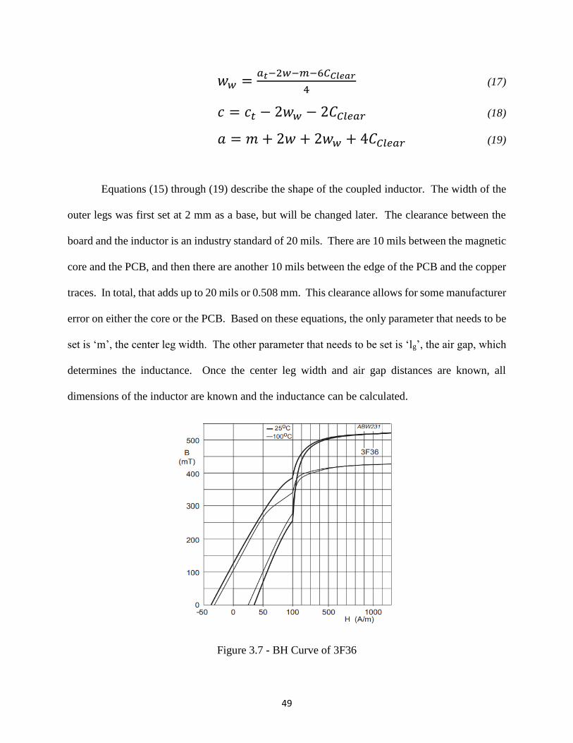
49
𝑤𝑤 =𝑎𝑡−2𝑤−𝑚−6𝐶𝐶𝑙𝑒𝑎𝑟
4 (17)
𝑐 = 𝑐𝑡 − 2𝑤𝑤 − 2𝐶𝐶𝑙𝑒𝑎𝑟 (18)
𝑎 = 𝑚 + 2𝑤 + 2𝑤𝑤 + 4𝐶𝐶𝑙𝑒𝑎𝑟 (19)
Equations (15) through (19) describe the shape of the coupled inductor. The width of the
outer legs was first set at 2 mm as a base, but will be changed later. The clearance between the
board and the inductor is an industry standard of 20 mils. There are 10 mils between the magnetic
core and the PCB, and then there are another 10 mils between the edge of the PCB and the copper
traces. In total, that adds up to 20 mils or 0.508 mm. This clearance allows for some manufacturer
error on either the core or the PCB. Based on these equations, the only parameter that needs to be
set is ‘m’, the center leg width. The other parameter that needs to be set is ‘lg’, the air gap, which
determines the inductance. Once the center leg width and air gap distances are known, all
dimensions of the inductor are known and the inductance can be calculated.
Figure 3.7 - BH Curve of 3F36

50
The next part of the design was to determine the saturation point of 3F36, the soft ferrite
chosen from Fig. 3.1. Fig. 3.7 shows the BH curve for 3F36 provided by Ferroxcube [14]. The
datasheets state that the absolute value for saturation is 420 mT, which is confirmed by Fig. 3.7.
However, as soon as the magnetic intensity reaches 100 A/m, the magnetic field rapidly increases
in a short amount of time, which is unpredictable. In order to simplify the calculation for the
magnetic field, the linear region of the BH curve was chosen to operate in. Assuming that the
magnetic core will heat up during operation, the curve for 100 °C is used, the maximum the
magnetic field can go before the curve leaves the linear region is 250 mT. For all calculations in
the inductor, if the magnetic field is ever to reach a value higher than 250 mT, then it is assumed
that inductor will be in saturation. Even if the magnetic field creeps a little bit higher than 250
mT, it is still considered in saturation. This will give enough wiggle room between the absolute
saturation and what is to be designed.
With the saturation point defined, he next step is to create the magnetic circuit for the
coupled inductor. Fig. 3.6 can be directly translated into a magnetic circuit, which is shown in
Fig. 3.8. The magnetic circuit is similar to that of a normal electrical circuit with resistances and
voltages. However in the magnetic circuit, there are reluctances, which are the air gaps, there are
magnetic motive forces, which are generated by the current and the windings, and finally there are
fluxes, which flow through the core. These can be directly translated from voltage, current, and
resistances to magnetic motive force, flux, and reluctance. In this coupled inductor, the reluctance
of the core is ignored because its reluctance compared to the air gap is much smaller and will have
little effect on the overall calculation.
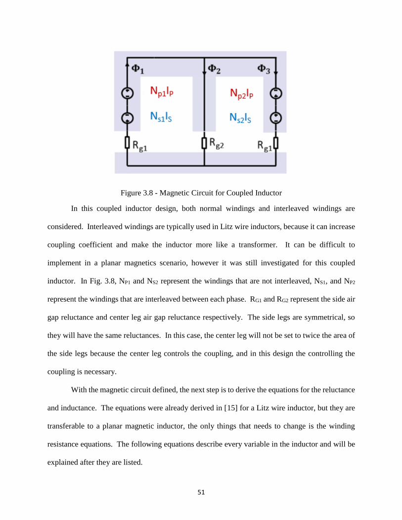
51
Figure 3.8 - Magnetic Circuit for Coupled Inductor
In this coupled inductor design, both normal windings and interleaved windings are
considered. Interleaved windings are typically used in Litz wire inductors, because it can increase
coupling coefficient and make the inductor more like a transformer. It can be difficult to
implement in a planar magnetics scenario, however it was still investigated for this coupled
inductor. In Fig. 3.8, NP1 and NS2 represent the windings that are not interleaved, NS1, and NP2
represent the windings that are interleaved between each phase. RG1 and RG2 represent the side air
gap reluctance and center leg air gap reluctance respectively. The side legs are symmetrical, so
they will have the same reluctances. In this case, the center leg will not be set to twice the area of
the side legs because the center leg controls the coupling, and in this design the controlling the
coupling is necessary.
With the magnetic circuit defined, the next step is to derive the equations for the reluctance
and inductance. The equations were already derived in [15] for a Litz wire inductor, but they are
transferable to a planar magnetic inductor, the only things that needs to change is the winding
resistance equations. The following equations describe every variable in the inductor and will be
explained after they are listed.
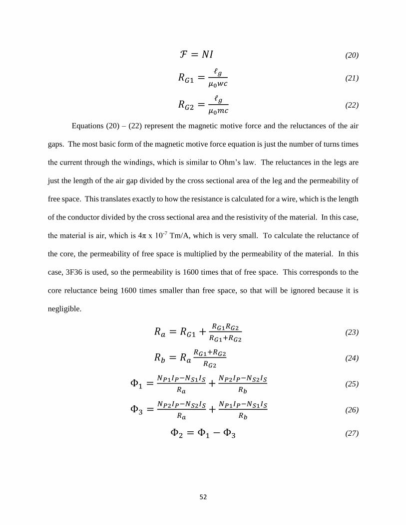
52
ℱ = 𝑁𝐼 (20)
𝑅𝐺1 =ℓ𝑔
𝜇0𝑤𝑐 (21)
𝑅𝐺2 =ℓ𝑔
𝜇0𝑚𝑐 (22)
Equations (20) – (22) represent the magnetic motive force and the reluctances of the air
gaps. The most basic form of the magnetic motive force equation is just the number of turns times
the current through the windings, which is similar to Ohm’s law. The reluctances in the legs are
just the length of the air gap divided by the cross sectional area of the leg and the permeability of
free space. This translates exactly to how the resistance is calculated for a wire, which is the length
of the conductor divided by the cross sectional area and the resistivity of the material. In this case,
the material is air, which is 4π x 10-7 Tm/A, which is very small. To calculate the reluctance of
the core, the permeability of free space is multiplied by the permeability of the material. In this
case, 3F36 is used, so the permeability is 1600 times that of free space. This corresponds to the
core reluctance being 1600 times smaller than free space, so that will be ignored because it is
negligible.
𝑅𝑎 = 𝑅𝐺1 +𝑅𝐺1𝑅𝐺2
𝑅𝐺1+𝑅𝐺2 (23)
𝑅𝑏 = 𝑅𝑎𝑅𝐺1+𝑅𝐺2
𝑅𝐺2 (24)
Φ1 =𝑁𝑃1𝐼𝑃−𝑁𝑆1𝐼𝑆
𝑅𝑎+
𝑁𝑃2𝐼𝑃−𝑁𝑆2𝐼𝑆
𝑅𝑏 (25)
Φ3 =𝑁𝑃2𝐼𝑃−𝑁𝑆2𝐼𝑆
𝑅𝑎+
𝑁𝑃1𝐼𝑃−𝑁𝑆1𝐼𝑆
𝑅𝑏 (26)
Φ2 = Φ1 − Φ3 (27)

53
Equations (23) through (27) all go into calculating the flux through each leg of the inductor.
Both equations (23) and (24) are just combinations of the reluctances that are used to calculate the
flux and inductances. The general way to calculate the flux is to take the magnetic motive force
and divide by the reluctance. To solve for the self-inductance of one leg of the inductor, the
opposite leg source is turned off and the flux can be calculated. For instance, to solve for the left
leg inductance and flux, all of the sources that include the right side inductor are turn off, NS1 and
NS2, while NP1 and NS1 are kept on. Then the inductance can be solved for by using Kirchoff’s
voltage and current law. Since both of the outer legs are identical, once one leg has been solved
for, and then the other leg is automatically known. To solve for the mutual inductance between
both side legs, the left leg source is kept on and right leg source is still off. Instead of solving for
the flux in the left leg, the flux in the right leg is solved for while still using the windings in the
left leg as a source. The process is similar for the leakage inductance; one can solve for the flux
in the center leg and repeat the process [16]. The following equations describe the self-inductance
and mutual inductance.
𝐿𝐿𝑒𝑓𝑡 =𝑁𝑃1
2+𝑁𝑃22
𝑅𝑎+
2𝑁𝑃1𝑁𝑃2
𝑅𝑏 (27)
𝐿𝑅𝑖𝑔ℎ𝑡 =𝑁𝑆1
2+𝑁𝑆22
𝑅𝑎+
2𝑁𝑆1𝑁𝑆2
𝑅𝑏 (28)
𝑀 =𝑁𝑃1𝑁𝑆1+𝑁𝑃2𝑁𝑆2
𝑅𝑎+
𝑁𝑃2𝑁𝑆1+𝑁𝑃1𝑁𝑆2
𝑅𝑏 (29)
𝛼 = −𝑀
𝐿 (30)
Equations (27) through (29) describe the self-inductance of the side legs and the mutual
inductance between them. Equation (30) describes the coupling coefficient between the mutual

54
and self-inductance. Since the core is symmetrical and the excitation going into each phase is
expected to be perfectly balanced, the left leg inductance and right leg inductance are identical.
The overall goal of designing the magnetics is to optimize the inductors to achieve the highest
efficiency and power density. Knowing everything about the inductance of the core is the first
part of the optimization. By knowing the inductance, the peak and valley of the current waveform
is known, then the turn on and turn off current is known, which can then be used to calculate the
switching loss of the devices. In addition, with a known inductance, the RMS value of the current
can be calculated and the conduction loss is known. With the inductance known, everything from
chapter two can be calculated and the entire device loss for four-phase interleaving is known.
The next part in the loss calculation is to calculate the core loss for the inductor. Core loss
can be difficult to calculate because the traditional way to calculate it is to use the Steinmetz
equation. However, the Steinmetz equation is based entirely off experimental data, so depending
on what material is chosen, the coefficients for the equation need to be given by either the
manufacturer or need to be experimentally taken. Another limitation of the Steinmetz equation is
that it is specifically designed for sinusoidal excitation. The equation is meant to be used for
transformers and transformers can only be used under sinusoidal excitation. The difference with
an inductor is that voltage across the inductor is in the shape of a square wave, which translates to
the current being a triangle shape. If the current is a triangular wave then the magnetic field of the
core will also be triangular as shown previously by Fig. 3.4. In order to calculate the core loss, a
modified equation needs to be derived.
𝑃𝑣 = 𝑘 ∗ 𝑓𝛼 ∗ 𝐵𝛽 (31)
Equation (31) describes the original Steinmetz equation. The Steinmetz equation is an
empirical equation, meaning that it is found through curve fitting measured data. There are three

55
coefficients: k, α, and β, which are found through curve fitting experimental data. Usually the
coefficients are given by the manufacturer, but if they are not, one would have to test a sample
core with sinusoidal excitation an curve fit the measured data. The other two variables, f and B,
are the frequency of the magnetic field and the magnitude of the magnetic field respectively. In
the case of the coupled inductor, there will be two separate frequencies in the core. The center leg
operates at twice the frequency of the outer legs because the leakage flux is additive as shown by
Fig. 3.2. The magnetic field will be changing with time as the current changes through the
inductor, however to calculated the core loss, the maximum value of the magnetic field is used in
the Steinmetz equation.
However, equation (31) only describes the core loss for sinusoidal excitation. The work
described in [17] can be used to calculate the core loss for non-sinusoidal excitation. In this paper,
the core loss can now be calculated for triangular wave magnetic fields. The triangular wave
magnetic field come from a square wave voltage excitation, which is based on the duty cycle of
the buck converter. In the paper, the Steinmetz equation was able to be modified so that the duty
cycle is now an input into the equation, which will allow for the core loss to be calculated for the
inductor being designed.
𝑃𝑣 =𝜋
4∗ 𝑘𝑑𝑎 ∗ 𝑘 ∗ 𝑓𝛼 ∗ 𝐵𝛽 (32)
𝑘𝑑𝑎 = 2−𝛼(𝐷(1−𝛼) + (1 − 𝐷)(1−𝛼)) (33)
Equation (32) is the new empirical method for the Steinmetz equation. The only difference
is that there are two new scaling factors to the original Steinmetz equation. Equation (33) describes
the scaling factor that is effected by the duty cycle. The new scaling factor is affected by α, which
is given by the manufacturer, and D, which is the duty cycle of the buck converter. With the new

56
empirical Steinmetz equation, the core loss can now be calculated for a specific operating point of
the buck converter. There is also the assumption that DC bias has little effect in the linear region
of the BH curve (area where the converter will be operating). Most of the current running through
the windings in the inductor is DC, but the Steinmetz equation calculates for sinusoidal excitation.
However, the paper was able to match experimental core loss closely with the new empirical
Steinmetz equation.
Table 3.1 - Material Coefficients for 3F36
Material Frequency
Minimum
Frequency
Maximum k α β C2 C1 C0
3F36 100000 499999 6.830 1.439 3.267 8.39e-5 0.0108 1.233
3F36 500000 799999 1.12e-4 2.195 2.720 8.93e-5 0.0117 1.282
3F36 800000 1200000 2.24e-7 2.611 2.498 6.12e-5 0.0061 1.011
Table 3.1 includes the material coefficients for the Steinmetz equation to calculate core
loss. One thing to note is that there are different coefficients for different frequencies that the core
experiences excitation. In the case for the coupled inductor being designed, the center leg
frequency will be twice that of the side leg frequencies. If the switching frequency of the buck
converter is larger than 250 kHz, two separate sets of coefficients will need to be used to calculate
the core loss. There are also three other coefficients that describe how the core operates under
certain temperatures.
𝑃𝑣 =𝜋
4∗ 𝑘𝑑𝑎 ∗ 𝑘 ∗ 𝑓𝛼 ∗ 𝐵𝛽 ∗ (𝐶2𝑇2 − 𝐶1𝑇 + 𝐶0) (34)
Equation (34) is the same empirical Steinmetz equation except that it has an extra equation
modifying it. The C coefficients are given in Table 3.1 and the T variable is the operating
temperature of the core. Typically, the core loss of materials change with temperature, so it is
57
necessary to scale loss with a changing temperature. This equation is also gathered through
experimentation.
Figure 3.9 - Core Loss Density vs Temperature for 3F36
Fig. 3.9 shows the core loss density versus the operating temperature of the material 3F36.
Each curve on the graph is supplemented with an operating frequency and an operating magnetic
field. The general trend is that when the maximum magnetic field is increased, the core loss
density increases. Not much can be said about the switching frequency because neither of the
parameters stay constant when comparing 500 kHz to 1 MHz. It can said that when the switching
frequency increases, the magnetic core size decreases, so when multiplying the core loss density
by the volume, the overall loss could be less at a higher switching frequency. The one thing that
is common among all the curves is that there is an optimal operating temperature. When the
temperature of the core is approximately 80 °C, the core will exhibit the lowest core loss. It is
unclear as to how hot the core would get during normal operation, so it was decided that the
58
assumed core temperature at full load would be approximately 90 °C for optimization purposes.
The only way to get an accurate temperature would be to actually fabricate a core and calculate
the core loss over a varying temperature grade. This is well beyond the scope of this work and
was not considered.
Now that core loss equation is established and the shape of the core is known, the core loss
in watts can be calculated. In order to find the core loss in terms of watts, the core loss density
calculated by the empirical Steinmetz equation needs to be multiplied by the volume of the
physical core.
𝑉𝐶𝑜𝑟𝑒 = 𝑎 ∗ 𝑏 ∗ 𝑐 (35)
𝑉𝐶𝑒𝑛𝑡𝑒𝑟 = 𝑚 ∗ 𝑐 ∗ (𝑏 − 2𝑤) (36)
𝑉𝑂𝑢𝑡𝑒𝑟 𝐿𝑒𝑔𝑠 = 𝑎 ∗ 𝑏 ∗ 𝑐 − (𝑎 − 2𝑤) ∗ (𝑏 − 2𝑤) ∗ 𝑐 (37)
𝑃𝐶𝑜𝑟𝑒 = 𝑃𝑣𝑐𝑒𝑛𝑡𝑒𝑟𝑉𝐶𝑒𝑛𝑡𝑒𝑟 + 𝑃𝑣𝑜𝑢𝑡𝑒𝑟𝑉𝑂𝑢𝑡𝑒𝑟 𝐿𝑒𝑔𝑠 (38)
Equations (35) through (38) describe the volume of the specific core areas and the total
loss in watts of the core. A, b, and c represent the width of the core, the height of the core, and the
depth of the core respectively, while w represents the width of the side legs and m represents the
width of the center leg. Note that the top section, the side legs, and the I-bar of the coupled inductor
are all the same width, so w can be used for everything except for the center. The Pv for the side
legs, top section, and I-bar will all experience the same frequency, so that is the reason why the
outer legs are combined into one volume. The center leg operates at a higher frequency than the
outer legs, so the Pv of the center leg is separate and the volume is much smaller. To achieve the
total loss in watts for the core, the volume of each section is multiplied by the corresponding core
loss.
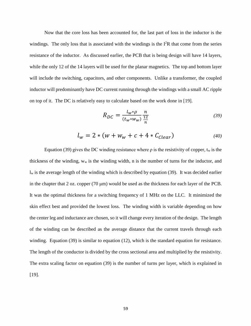
59
Now that the core loss has been accounted for, the last part of loss in the inductor is the
windings. The only loss that is associated with the windings is the I2R that come from the series
resistance of the inductor. As discussed earlier, the PCB that is being design will have 14 layers,
while the only 12 of the 14 layers will be used for the planar magnetics. The top and bottom layer
will include the switching, capacitors, and other components. Unlike a transformer, the coupled
inductor will predominantly have DC current running through the windings with a small AC ripple
on top of it. The DC is relatively easy to calculate based on the work done in [19].
𝑅𝐷𝐶 =𝑙𝑤∗𝜌
(𝑡𝑤∗𝑤𝑤)
𝑛12
𝑛
(39)
𝑙𝑤 = 2 ∗ (𝑤 + 𝑤𝑤 + 𝑐 + 4 ∗ 𝐶𝐶𝑙𝑒𝑎𝑟) (40)
Equation (39) gives the DC winding resistance where ρ is the resistivity of copper, tw is the
thickness of the winding, ww is the winding width, n is the number of turns for the inductor, and
lw is the average length of the winding which is described by equation (39). It was decided earlier
in the chapter that 2 oz. copper (70 μm) would be used as the thickness for each layer of the PCB.
It was the optimal thickness for a switching frequency of 1 MHz on the LLC. It minimized the
skin effect best and provided the lowest loss. The winding width is variable depending on how
the center leg and inductance are chosen, so it will change every iteration of the design. The length
of the winding can be described as the average distance that the current travels through each
winding. Equation (39) is similar to equation (12), which is the standard equation for resistance.
The length of the conductor is divided by the cross sectional area and multiplied by the resistivity.
The extra scaling factor on equation (39) is the number of turns per layer, which is explained in
[19].
60
Figure 3.10 - Average Length of Winding
Fig. 3.10 shows an aerial view of what the coupled inductor would look like. All of the
variable have already been defined and are shown on the left leg of the inductor. The right leg of
the inductor shows what the average length of the winding is defined as. Using this picture as an
example, the average length can be found and equation (40) is the result. This is the ideal case for
the average length, so when this is implemented, the average length will be a little bit longer.
When the PCB is designed, the current has to come from somewhere, so the average winding
length will increase a small amount, which will in turn increase the DC winding resistance.
However, this is unknown at the time of the inductor design and can only be estimated. It is

61
estimated to be an extra 10 mm, because the two measurement ports for the beginning and end of
the inductor will be a small distance from the actual inductor and not directly on top of it.
Now that the DC winding resistance is known, the final part of the loss calculation is to
find the total winding loss. The current running through the inductor windings is a triangle type
waveform with a DC offset. This is not a standard case where the DC resistance can be multiplied
by some scaling factor to find the AC winding resistance and then then the total winding resistance
is known. The total winding resistance is difficult to calculate by hand, so in order to find it,
ANSYS Maxwell was used to simulate the total winding resistance. It may have seemed like a
waste of time to derive an equation for the DC winding resistance, however it is helpful when the
core is optimized to see how the DC winding resistance changes and the conduction loss on the
windings change. It is useful information even though simulation is used to get the final overall
result. It also helps to have an equation that can represent total winding loss because it can become
tedious to run a simulation for every iteration of the design. When a simulation takes five minutes
to setup and run, it adds up, so having an equation will help.
Figure 3.11 - Current Direction in ANSYS Maxwell

62
Fig. 3.11 shows what the inductor looks like constructed in a 2D ANSYS Maxwell
simulation and it shows the current direction in the windings. The gray part represents the core
and it is 3F36. ANSYS allows material parameters to be input into its solver, so the material
parameters provided by Ferroxcube for 3F36 were input into ANSYS, so the solver could know
core loss, saturation point, and the magnetic permeability of the material. The orange and blue
rectangles represent the windings of the inductor and they are both copper. ANSYS already
provides material parameters for copper, so nothing needs to be changed. There are 12 layers of
copper around each leg, where they represent the windings. The black circle describe the direction
of the current, the ‘x’ is for into the page and the dot is for out of the page. The current direction
represent inverse coupling of both inductors.
Figure 3.12 - Winding Groupings
Fig. 3.12 shows the same core depicted except there are two groupings of windings
highlighted. By grouping these pieces of copper together, it will tell ANSYS that these are all the
same conductor, so current will flow between them. In this case, two windings are grouped
together meaning that this is a six-turn inductor. It is assumed that current is perfectly balanced
between parallel winding layers, so when the current is assigned to each winding, it will be divided

63
by how many parallel layers are grouped together. For example, if the expected current through
the windings is supposed to be 10 A, then each parallel winding layer will be given a 5 A excitation.
Note that this is not the actual case, but in order to calculate total winding loss, having all static
variables helps considerably. In Fig. 3.12, the winding groupings are repeated for the second
inductor, with perfect current sharing as the assumption. The current balancing issue will be
addressed later. In the case displayed, there would be six groupings of windings for the left leg
inductor and six groupings of windings for the right leg inductor. Both current excitations will be
exactly the same for each inductor with a phase shift of 180° to emulate the buck converter in
operation.
A very important consideration for all of the magnetic simulation done for this design is
that only 2D simulation is used. ANSYS Maxwell has three different solvers: magneto-static,
eddy-current, and transient analysis. Magneto-static simulation is used when the excitation is DC,
eddy-current is used when the excitation is sinusoidal, and the transient solver is used for every
other excitation. One of the limitations of Finite Element Analysis (FEA) is that a large amount
of memory is required to run simulations. In the lab that this research was conducted, only 16 GB
of RAM was available to run the simulations on. This is a very insignificant amount of memory
to run simulations on in terms of 3D. This is a sufficient amount of memory to run 2D simulations,
however to run 3D simulations the computers cannot handle the computations and it would take
upwards of weeks for a single simulation to run, which is too long for the scope of this project. In
the case of the inductor being designed, transient simulation is necessary to simulate the non-
sinusoidal current and non-DC current. All simulations for the inductors will be run in 2D, so
there could be some discrepancies between experimental and simulated results due to
64
computational limitations. However, if a dedicated server or super computer is used to run
simulations, there would be no problem in terms of simulation time.
To find the total winding loss, an ANSYS simulation will be run and the loss in watts will
be given from the simulation. In order to make an equation for total loss, the parameters of the
inductor needs to change, but changing the inductor dimensions can skew the loss given by
ANSYS. In order to combat this, the dimension will be fixed for the inductor and only the air gap
will change when calculating the winding loss. If only the air gap changes, then the inductance
will change, but keep the same dimensions for the windings. If the inductance changes, that means
the peak-to-peak of the current will also change, while keeping the same DC offset. A relationship
can be formed between the DC winding resistance and the total winding resistance. By using the
change in current ripple, a scaling factor FR can be found and used to translate between the two.
With the total winding resistance known, the loss for the windings can be found by multiplying by
the RMS current.
𝑃𝑊𝑖𝑛𝑑𝑖𝑛𝑔 = 𝐼𝑅𝑀𝑆2 ∗ 𝑅𝐷𝐶 ∗ (𝐹𝑅 + 1) (41)
𝐹𝑅 =𝑃𝑊𝑖𝑛𝑑𝑖𝑛𝑔
𝐼𝑅𝑀𝑆2𝑅𝐷𝐶
− 1 (42)
Equation (41) represents the total winding loss in watts. The equation consists of the DC
winding loss plus the DC winding loss scaled by FR. Traditionally, FR is the relationship between
AC and DC resistance, but in this case, it is the scaling between the DC winding resistance and the
resistance that is caused by the triangle excitation. Equation (42) describes how the scaling factor
is found. ANSYS will give the total loss, PWinding, the DC winding resistance is already known,
and the RMS current is known because the inductance is known. The scaling factor FR can then
be plotted against the ripple current to find an equation that can be used for all cases.

65
Figure 3.13 - FR at Different Number of Turns
Fig. 3.13 shows the peak-to-peak current squared versus the scaling coefficient FR. The
values further to the right correspond to a smaller inductance because the peak-to-peak value of
the current is larger and vice-versa for the left side values. In the figure, each curve looks to be
similar even when the turns number is changed. However, the equation calculated from the line
of best fit are slightly different in terms of their y-intercept. This is an example of how the winding
loss is calculated a different turns numbers. There minor differences between the curves is due to
the small differences in the dimensions of the core. If one were to look at the three turn curve, it
stops when the peak-to-peak current squared is only about 50 A. The reason why the curve stops
is because the inductance is getting too small and it is hitting the saturation value, so the inductor
cannot physically operate under the nominal condition, so that solution is not viable to use. As the
turns number decreases, the core reaches saturation faster at smaller inductances, which can be
0
0.2
0.4
0.6
0.8
1
1.2
0 20 40 60 80 100 120 140
FR
Ipp2 (A2)
FR at Different Turns for Coupled Inductor
6 Turns
4 Turns
3 Turns

66
explained by the equations earlier in the chapter. When the turns number is changed, the power
loss in the windings does not seem to change too much.
Figure 3.14 - FR at Different Frequencies
Fig. 3.14 shows the same type of graph as Fig. 3.13 except that now the switching
frequency is changing for the coupled inductor. This is just to prove that for every case the scaling
coefficient, FR, will need to be re-evaluated. Whether the switching frequency or the turns number
changes, the scaling factor does not stay the same. In this case, as the switching frequency
increases, the scaling factor also increases, which means that the total loss will increase for the
windings. The reason why the winding resistance increases with increase switching frequency is
because of the increased eddy current effects [20]. More eddy currents are induced at higher
switching frequencies, which in turn will induce larger losses in the current portion of I2R losses.
The simulations performed give the copper loss in watts, which includes both current and
resistance. Even though the current stays the same value, eddy currents will be induced from the
-0.2
0
0.2
0.4
0.6
0.8
1
0 50 100 150 200
FR
Ipp2 (A2)
FR at 6 Turns Coupled Inductor
500 kHz
400 kHz

67
skin effect and proximity effect, which are not measurable, but they still contribute to the loss.
Even though the total resistance increases, it does not give the whole story, the switching frequency
increases eddy currents, which increases the loss but only shows up in the resistance of the
windings. However, even though the calculated resistance might not be representative of the actual
resistance, it still encompasses the actual loss seen by the windings.
The winding resistance was the final component of the losses in the buck converter. With
every loss accounted for, an optimization model can be made and used to find best core size for
the project. The optimization will happen around two variables, the coupling coefficient and the
inductance. The coupling coefficient is controlled by sweeping the center leg width and the
inductance is controlled by sweep the air gap of the inductor. With all parameters known, the
following optimization chart can be made:

68
Figure 3.15 - Magnetic Optimization Flow Chart
Fig. 3.15 shows the flow chart for how the coupled inductor core will be optimized. The
first step in the optimization is to start with a footprint from which the maximum bounds for the
inductor plus windings can be set. The next step is to set the switching frequency and number of
turns, which will be used to determine the equation for the total winding resistance. Once the turns
ratio and turns are known, one can go to ANSYS to determine the total winding loss and find a
scaling factor between the DC winding resistance and total winding resistance. Next, the
inductance is swept, which will be determined by finding the air gap that corresponds with the set
inductance. In practice, it can be difficult to get the exact thickness of the air gap, so there will be
slight error when implementing the air gap on the actual core. After the inductance is swept, the
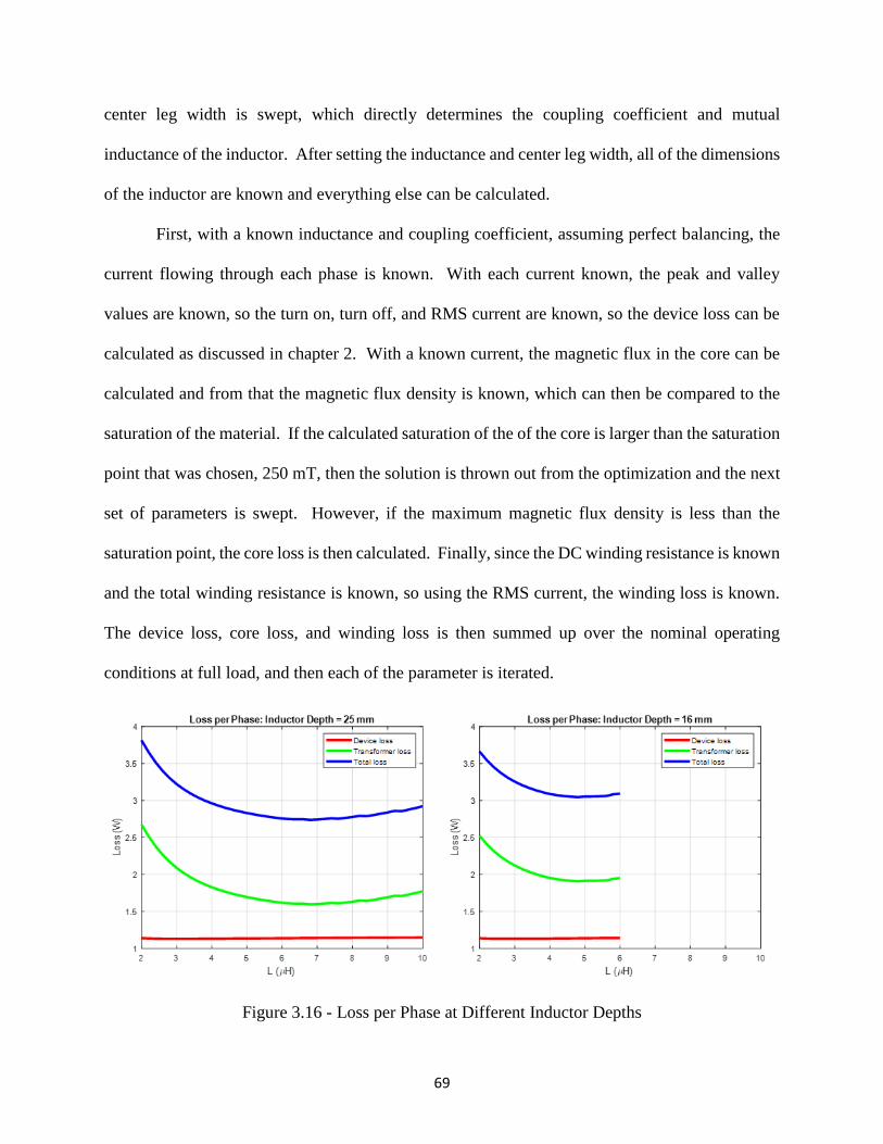
69
center leg width is swept, which directly determines the coupling coefficient and mutual
inductance of the inductor. After setting the inductance and center leg width, all of the dimensions
of the inductor are known and everything else can be calculated.
First, with a known inductance and coupling coefficient, assuming perfect balancing, the
current flowing through each phase is known. With each current known, the peak and valley
values are known, so the turn on, turn off, and RMS current are known, so the device loss can be
calculated as discussed in chapter 2. With a known current, the magnetic flux in the core can be
calculated and from that the magnetic flux density is known, which can then be compared to the
saturation of the material. If the calculated saturation of the of the core is larger than the saturation
point that was chosen, 250 mT, then the solution is thrown out from the optimization and the next
set of parameters is swept. However, if the maximum magnetic flux density is less than the
saturation point, the core loss is then calculated. Finally, since the DC winding resistance is known
and the total winding resistance is known, so using the RMS current, the winding loss is known.
The device loss, core loss, and winding loss is then summed up over the nominal operating
conditions at full load, and then each of the parameter is iterated.
Figure 3.16 - Loss per Phase at Different Inductor Depths

70
Fig. 3.16 shows the plot of the inductance versus the loss per phase of each inductor in the
optimization. The results were shown in phase comparison, just so one could multiply the losses
by two to get a single inductor loss or by four to get the overall loss for the buck converter. The
side leg width is set at 2 mm, with a turns number of six. For the following figures, these two
parameters are set and will not change. Two separate core and winding depths are shown, 16 mm
and 25 mm. The device loss includes the turn on, turn off, and conduction losses. The transformer
loss includes the core loss and winding loss and the total loss is everything summed up. This plot
shows that at a certain footprint size, there will be a specific inductance that will give the lowest
loss over the entire range. On the left at 25 mm inductor depth, the inductance is able to be swept
over the entire range from 2 μH to 10 μH, where the inductor depth on the left of 16 mm is unable
to achieve anything higher than 6 μH. The reason for this is that the inductor on the graph on the
right is reaching saturation when high inductances are desired. The reason the inductor is
saturating is that the core is smaller, so the cross sectional area of each leg is smaller, which will
raise the magnetic flux density. In order to achieve higher inductances, the air gap needs to be
smaller, which will lower the reluctances of the legs, which in turn will increase the flux running
through the core. If the flux is larger and the cross sectional area is smaller, that equates to a higher
magnetic flux density, which could possibly pass over saturation. In the case of six turns and two
mm leg width, the inductor starts to saturate when the overall inductor depth is at 21 mm. Lastly,
the device loss stays constant over all inductances, only increasing slightly as the inductance
increases. This is due to the fact as the inductance changes, the ripple will change, which means
the turn off loss will decrease but the turn on loss will increase. The equations are similar in terms
of magnitude, with the turn equation carrying slightly more weight than the turn off equation.

71
There is a slight increase, but it is too small to see as it only increases about 0.1 W over the whole
range.
Looking at Fig. 3.16 there is an optimal point for minimum loss. By following Fig. 3.15,
the next step in the optimization is to sweep the footprint area. The way the footprint area is swept
is the depth of the inductor, ct, will be increased and decreased and each optimal point will be
chosen.
Figure 3.17 - Loss vs. Core Depth and Efficiency vs. Power Density
Fig. 3.17 shows two figures, the one on the left is the total loss of the four-phase converter
plotted versus inductor depth and the graph on the left is the power density versus buck converter
efficiency. Both figure shows the same data, just in a slightly different way. The graph on the left
makes it easier to see what inductor depth gives the lowest loss over all of the cases swept, while
the graph on the right shows which converter gives the best efficiency while considered converter
size. The converter size is known because in chapter 2, the layout of the switching was already
determined and by using a PCB layout software, the size of the switching and input capacitors can
be found, which then can be added to the inductor depth, and then the power density can be found.
𝐸𝑓𝑓𝑖𝑐𝑖𝑒𝑛𝑐𝑦 =𝑃𝑂
𝑃𝑂+𝑃𝐿𝑜𝑠𝑠 (43)

72
𝑃𝐷𝑒𝑛𝑠𝑖𝑡𝑦 =𝑃𝑂∗𝐸𝑓𝑓𝑖𝑐𝑖𝑒𝑛𝑐𝑦
𝑉𝐵𝑜𝑎𝑟𝑑 (44)
Equations (43) and (44) shows how the efficiency and power density were calculated. Po
describes the output power of the converter, which is 1000 W for all cases. PLoss is the total loss
of the entire converter, which can be shown by Fig. 3.17. VBoard describes the volume of the buck
converter, which is the inductor added with the 7.1 mm used for the switches. Both of these
equations are used to calculate the curves in Fig. 3.17. In Fig. 3.17, for the graph that depicts the
power density, as the curve goes to a higher power density, the size of the core shrink, which leads
to a smaller efficiency. This is directly attributed to the core loss, which can be shown in Fig. 3.18.
Figure 3.18 - Loss Breakdown at Varying Depths
Fig. 3.18 shows the loss breakdown for the buck converter over varying depths of the
inductor. When the inductor is smaller or ct is smaller, the core loss is much larger than at other

73
depths. The is because as the core gets smaller, the cross sectional area is smaller, so the magnetic
flux density increases, which in turn increases the core loss. As the inductor grow larger, the
winding loss starts to dominate the losses because as the inductor grows in size, the winding
resistance increases and the conduction loss starts to dominate from the inductor. The device loss
stays constant over all depths, only increasing marginally, which has been explained earlier.
Figure 3.19 - Inductance vs Varying Depth
Fig. 3.19 shows how the inductance changes versus the inductor size. Each point represents
the most optimal point at each depth. There is no surprise that as the inductor size increases; the
most optimal point will have a larger inductance. This allows for larger core legs, so the cross
sectional area is larger, while the air gap can be made smaller. With that combination, the magnetic
flux density of the core can be pushed closer to saturation, while keeping the inductance at a large
value. This can be helpful if one is worried about the peak-to-peak steady state current value.
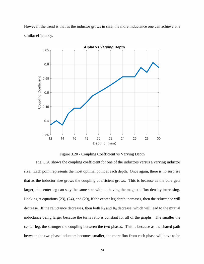
74
However, the trend is that as the inductor grows in size, the more inductance one can achieve at a
similar efficiency.
Figure 3.20 - Coupling Coefficient vs Varying Depth
Fig. 3.20 shows the coupling coefficient for one of the inductors versus a varying inductor
size. Each point represents the most optimal point at each depth. Once again, there is no surprise
that as the inductor size grows the coupling coefficient grows. This is because as the core gets
larger, the center leg can stay the same size without having the magnetic flux density increasing.
Looking at equations (23), (24), and (29), if the center leg depth increases, then the reluctance will
decrease. If the reluctance decreases, then both Ra and Rb decrease, which will lead to the mutual
inductance being larger because the turns ratio is constant for all of the graphs. The smaller the
center leg, the stronger the coupling between the two phases. This is because as the shared path
between the two phase inductors becomes smaller, the more flux from each phase will have to be

75
shared in the mutual path. The center leg gives more area for flux to escape from the shared path
and is only used to control coupling.
Figure 3.21 - DC Winding Resistance vs Inductance
Fig. 3.21 shows the DC winding resistance versus the inductance. Each point represents a
point when the inductor depth is 22 mm. The reason why the DC winding resistance is changing
is because this is plotted when the center leg, m, is being swept. The center leg is changing slightly
every design, so there is a slight change in the average length in each winding, which is enough to
change the DC winding resistance by a few mΩ. There is an optimal DC winding resistance when
the center leg is swept and when the inductance increases, so does the DC winding resistance. This
is because when the inductance increases past a certain point, the coupling coefficient starts to
decrease, shown in Fig. 3.22, which means that the center leg width is decreasing. If the center
leg width decreases, then the windings have a larger average length while keeping the same cross

76
sectional area, which means that the DC winding resistance will be slightly larger. Before the
smallest DC winding resistance, the coupling coefficient starts increasing until the most optimal
point, which means that the center leg is smaller, making the average winding length slightly
larger.
Figure 3.22 - Coupling Coefficient vs Inductance
Fig. 3.22 shows the coupling coefficient versus the inductance. Each point represents a point
when the inductor depth is 22 mm. This plot is the exact opposite of the DC winding resistance plot.
When the coupling coefficient is the largest, the DC winding resistance is at its smallest. This is
because when the center leg is smallest, the coupling is the strongest, and the cross sectional area
of the windings is the largest. The coupling coefficient play an important role for coupled
inductors because it determines whether or not the steady state current ripple will be larger or
smaller than a normal inductor. If one refers back to equation (13), at nominal operation, the

77
coupling coefficient would have to be smaller than 0.33, to have the steady state current ripple of
the coupled inductor be smaller than the current ripple of the normal inductor without coupling.
From the graph above, the coupling coefficient does not even reach that low. This means that even
if the steady state current ripple of the coupled inductor is larger than that of a regular inductor, it
is still not the most optimal choice because Fig. 3.22 shows that a higher coupling coefficient gives
a better efficiency. The reason why a small coupling coefficient cannot be achieved is that the
coupling coefficient is smallest when the center leg is largest. If the center leg large with the same
inductor area, then the windings are smaller, which means the DC winding resistance will be large.
If the DC winding resistance is large, then winding loss becomes too dominant in the loss
breakdown to be beneficial to the entire optimization, which is shown in Fig. 3.18. Most likely,
the coupled inductor will not be able to decrease the steady state current ripple.
Figure 3.23 - Center Leg Width vs Inductance

78
Fig 3.23 is a plot of the center leg width versus the inductance. Each point represents a
point when the inductor depth is 22 mm. This plot is just to highlight the relationship between the
coupling coefficient and the center leg width. Comparing this to Fig. 3.22, when the center leg
width is the smallest, the coupling coefficient at its highest. When the mutual flux has less area
for the mutual flux to escape to, then the coupling is higher because the mutual flux stays in the
same path. If the equation (13) were to be satisfied, then the center leg width would have to be
very large in order to get a small coupling coefficient. This would impractical however because it
would raise the DC winding resistance to where the winding loss dominates all loses and becomes
unbeneficial to the whole system.
The previous eight figures that have been shown are all under the same parameters: side
leg width of 2 mm, switching frequency of 500 kHz, each inductor has six turns with no
interleaving and perfect current balancing. This only represents a fraction of the cases that this
inductor could go under. There can be multiple different turn numbers, the side leg width can be
changed, and the switching frequency can change. The upcoming charts will show comparisons
of all cases, to show which one can provide the best performance. Even though one case may
shows better efficiency than another, there are still other real world considerations that need to be
taken into effect, so the converter can run optimally.

79
Figure 3.24 - Inductor Loss per Phase vs Inductance
Fig. 3.24 shows the loss per phase of the inductors at a core depth of 22 mm similar to that
in Fig. 3.16. The main difference is that in these plots, the loss for both 500 kHz and 400 kHz is
shown in comparison. 500 kHz is the solid line and 400 kHz is the dashed line. By looking at the
graphs, 400 kHz clearly produces less loss than a switching frequency of 500 kHz, which is
dominated by the winding loss. The winding loss is lower for 400 kHz because of less eddy
currents in the windings, which has been explained earlier. The device loss is also lower than 500
kHz because the turn on energy is multiplied by the switching frequency and 500 kHz is much
larger than 400 kHz. Even though the current peak and valley is larger with the 400 kHz case,
there is more loss with higher switching frequencies. Lastly, the core loss did increase for the
lower switching frequency. This is expected because there is a higher peak-to-peak current ripple
at lower frequencies, which means the di/dt for the magnetic flux density is higher. With higher
di/dt and the same core area, the magnetic flux density will be higher, which will cause the core
loss to be higher when using the Steinmetz equation proposed earlier.
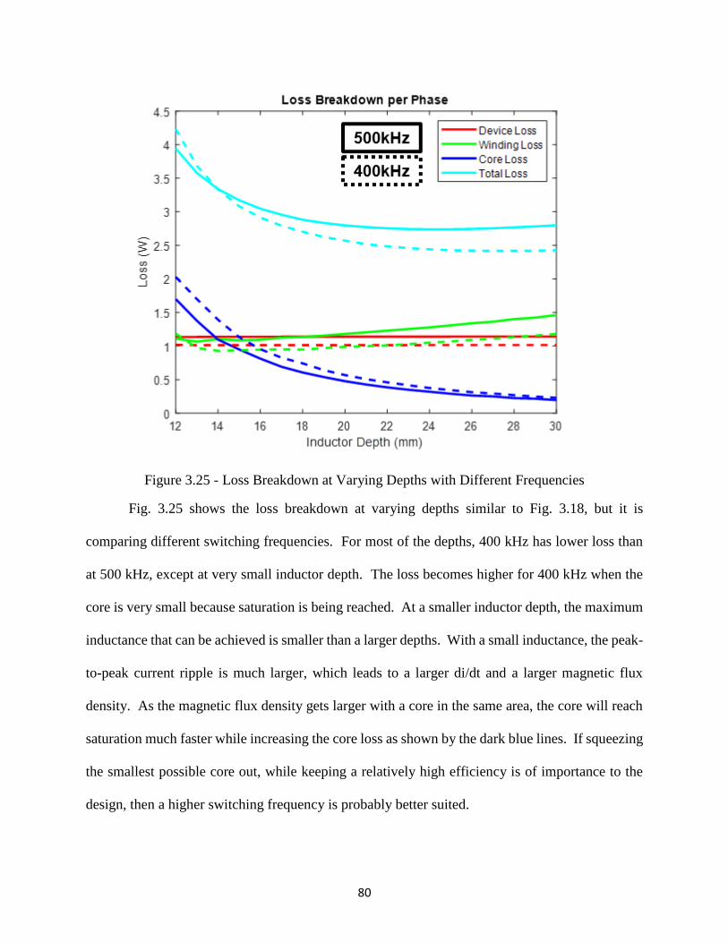
80
Figure 3.25 - Loss Breakdown at Varying Depths with Different Frequencies
Fig. 3.25 shows the loss breakdown at varying depths similar to Fig. 3.18, but it is
comparing different switching frequencies. For most of the depths, 400 kHz has lower loss than
at 500 kHz, except at very small inductor depth. The loss becomes higher for 400 kHz when the
core is very small because saturation is being reached. At a smaller inductor depth, the maximum
inductance that can be achieved is smaller than a larger depths. With a small inductance, the peak-
to-peak current ripple is much larger, which leads to a larger di/dt and a larger magnetic flux
density. As the magnetic flux density gets larger with a core in the same area, the core will reach
saturation much faster while increasing the core loss as shown by the dark blue lines. If squeezing
the smallest possible core out, while keeping a relatively high efficiency is of importance to the
design, then a higher switching frequency is probably better suited.
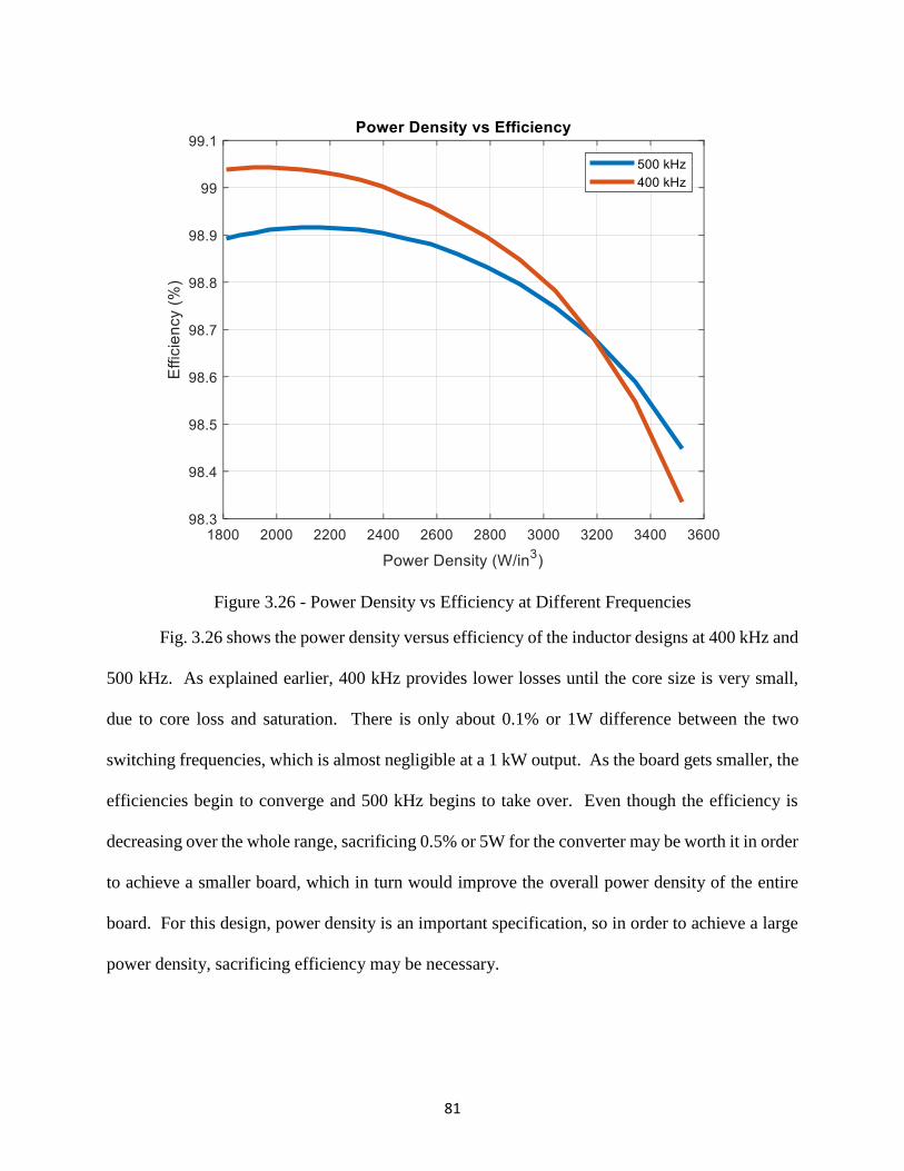
81
Figure 3.26 - Power Density vs Efficiency at Different Frequencies
Fig. 3.26 shows the power density versus efficiency of the inductor designs at 400 kHz and
500 kHz. As explained earlier, 400 kHz provides lower losses until the core size is very small,
due to core loss and saturation. There is only about 0.1% or 1W difference between the two
switching frequencies, which is almost negligible at a 1 kW output. As the board gets smaller, the
efficiencies begin to converge and 500 kHz begins to take over. Even though the efficiency is
decreasing over the whole range, sacrificing 0.5% or 5W for the converter may be worth it in order
to achieve a smaller board, which in turn would improve the overall power density of the entire
board. For this design, power density is an important specification, so in order to achieve a large
power density, sacrificing efficiency may be necessary.
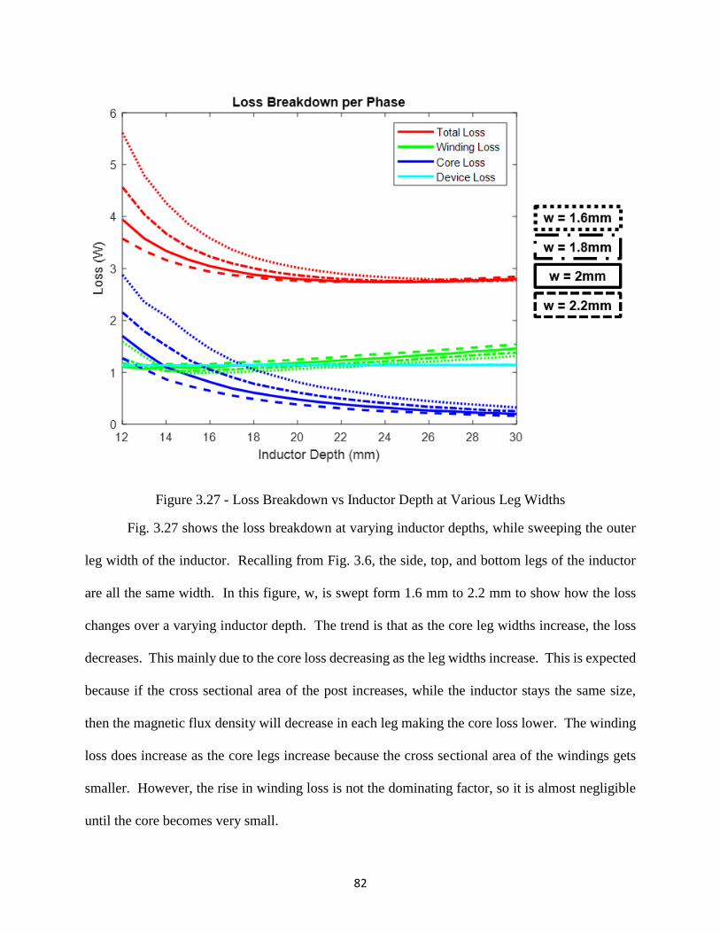
82
Figure 3.27 - Loss Breakdown vs Inductor Depth at Various Leg Widths
Fig. 3.27 shows the loss breakdown at varying inductor depths, while sweeping the outer
leg width of the inductor. Recalling from Fig. 3.6, the side, top, and bottom legs of the inductor
are all the same width. In this figure, w, is swept form 1.6 mm to 2.2 mm to show how the loss
changes over a varying inductor depth. The trend is that as the core leg widths increase, the loss
decreases. This mainly due to the core loss decreasing as the leg widths increase. This is expected
because if the cross sectional area of the post increases, while the inductor stays the same size,
then the magnetic flux density will decrease in each leg making the core loss lower. The winding
loss does increase as the core legs increase because the cross sectional area of the windings gets
smaller. However, the rise in winding loss is not the dominating factor, so it is almost negligible
until the core becomes very small.
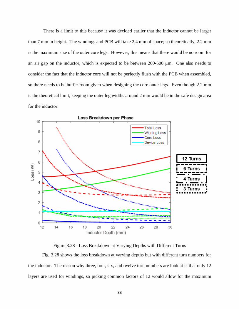
83
There is a limit to this because it was decided earlier that the inductor cannot be larger
than 7 mm in height. The windings and PCB will take 2.4 mm of space; so theoretically, 2.2 mm
is the maximum size of the outer core legs. However, this means that there would be no room for
an air gap on the inductor, which is expected to be between 200-500 μm. One also needs to
consider the fact that the inductor core will not be perfectly flush with the PCB when assembled,
so there needs to be buffer room given when designing the core outer legs. Even though 2.2 mm
is the theoretical limit, keeping the outer leg widths around 2 mm would be in the safe design area
for the inductor.
Figure 3.28 - Loss Breakdown at Varying Depths with Different Turns
Fig. 3.28 shows the loss breakdown at varying depths but with different turn numbers for
the inductor. The reason why three, four, six, and twelve turn numbers are look at is that only 12
layers are used for windings, so picking common factors of 12 would allow for the maximum

84
utilization of all layers. If one was to use four turns, then they could parallel three layers to share
current. At first look, a coupled inductor with six turns provides the least amount of loss over the
varying inductor lengths, until the core becomes very large. By looking at the core loss, as the
turns number increases, the core loss decreases. This is because the inductance is directly
proportional to the square of the turns number. This means for a higher turns number, a larger
inductance can be achieved at all inductor depths. At the smallest inductor depth, a 12 turn
inductor is able to achieve 5.5 μH, while the smaller turn inductor is only able to achieve 2 μH.
With a smaller di/dt, the magnetic flux density decreases, which will give a smaller core loss. With
a larger inductance, the peak-to-peak current ripple decreases, which in turn decreases the di/dt in
each of the legs of the inductor. Another major loss contributor is the winding loss. As the turns
number increases, the winding loss also increases over all cases, with a huge jump in losses from
six turns to twelve turns. The reason why the winding loss increases as turns number increases is
that the winding resistance increases. With smaller turn numbers, the windings can be paralleled,
which would lead to paralleling resistances for the windings, which decreases the overall winding
resistance. By looking at equation (39), if one uses 12 turns, the resistance is multiplied by 12, but
if one is to use six turns, then the equation is only multiplied by three, so there is a major increase
in winding resistance from six to twelve turns. That is why there is a huge jump in loss from six
to twelve turns.
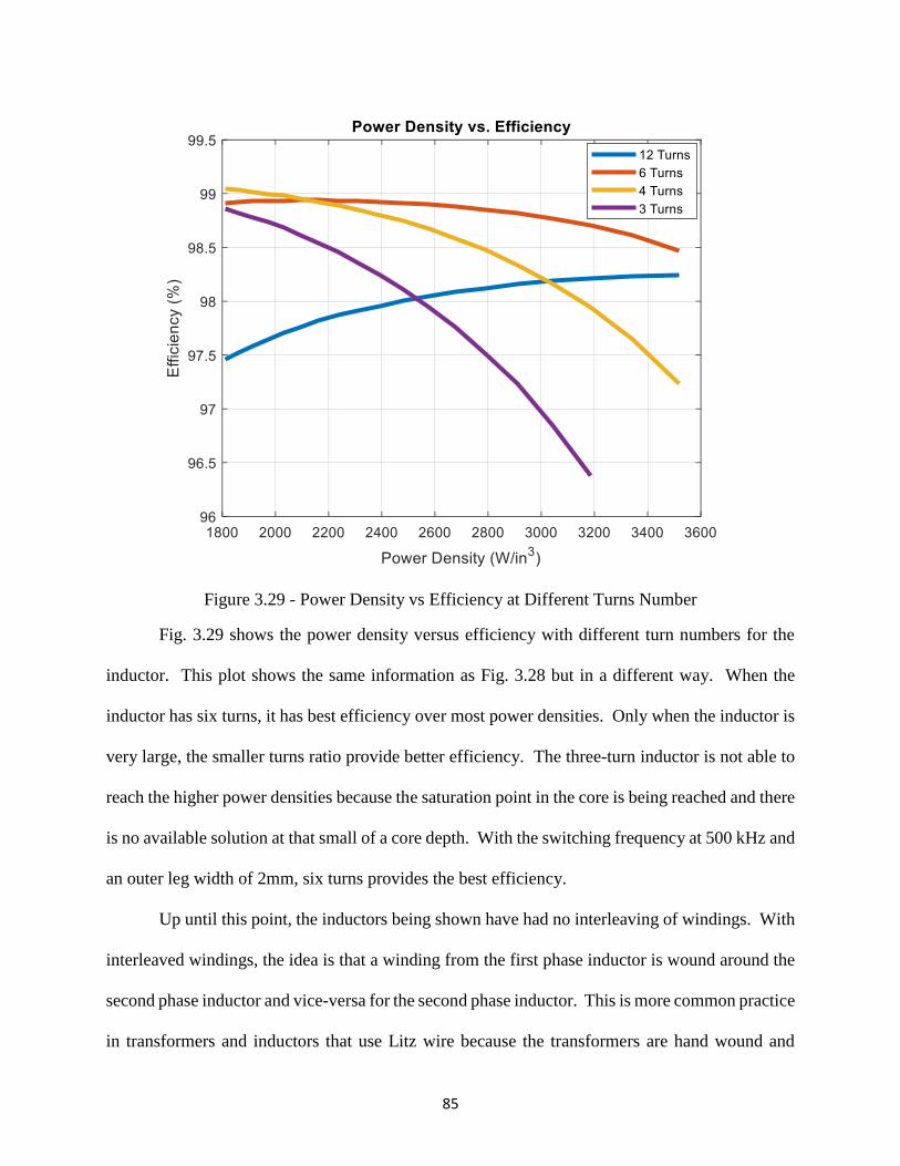
85
Figure 3.29 - Power Density vs Efficiency at Different Turns Number
Fig. 3.29 shows the power density versus efficiency with different turn numbers for the
inductor. This plot shows the same information as Fig. 3.28 but in a different way. When the
inductor has six turns, it has best efficiency over most power densities. Only when the inductor is
very large, the smaller turns ratio provide better efficiency. The three-turn inductor is not able to
reach the higher power densities because the saturation point in the core is being reached and there
is no available solution at that small of a core depth. With the switching frequency at 500 kHz and
an outer leg width of 2mm, six turns provides the best efficiency.
Up until this point, the inductors being shown have had no interleaving of windings. With
interleaved windings, the idea is that a winding from the first phase inductor is wound around the
second phase inductor and vice-versa for the second phase inductor. This is more common practice
in transformers and inductors that use Litz wire because the transformers are hand wound and
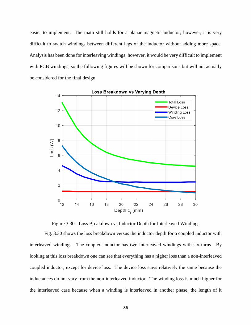
86
easier to implement. The math still holds for a planar magnetic inductor; however, it is very
difficult to switch windings between different legs of the inductor without adding more space.
Analysis has been done for interleaving windings; however, it would be very difficult to implement
with PCB windings, so the following figures will be shown for comparisons but will not actually
be considered for the final design.
Figure 3.30 - Loss Breakdown vs Inductor Depth for Interleaved Windings
Fig. 3.30 shows the loss breakdown versus the inductor depth for a coupled inductor with
interleaved windings. The coupled inductor has two interleaved windings with six turns. By
looking at this loss breakdown one can see that everything has a higher loss than a non-interleaved
coupled inductor, except for device loss. The device loss stays relatively the same because the
inductances do not vary from the non-interleaved inductor. The winding loss is much higher for
the interleaved case because when a winding is interleaved in another phase, the length of it

87
doubles. If the length of a conductor increases while keeping the same cross sectional area, then
its resistance increases. With increasing resistance, the loss will also increase. The core loss
increases because there is now a second a second current running through each phase leg, which
introduces a different magnetic flux in each leg. Take note that the current in each phase leg will
be exactly 180° out of phase with each other. Looking back at Fig. 3.3, the currents will in some
cases cancel each other out, during the time that LEQ3 is active, and other cases will add together,
during the time that LEQ2 is active. Even though some of the current is flowing in the opposite
direction, there is a brief moment where they are flowing in the same direction and the currents
add, which gives a larger magnetic flux density, which raises the loss on the core. For a core this
size, the increase in loss is expected, however for another size it may be beneficial to interleave
windings.
Figure 3.31 - Coupling Coefficient vs Inductor Depth
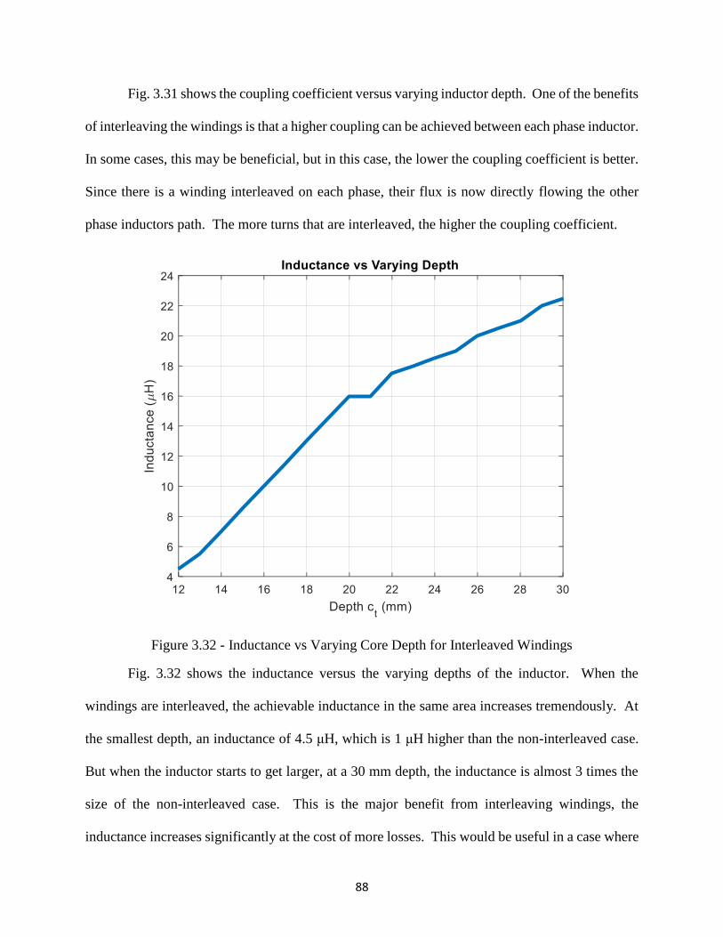
88
Fig. 3.31 shows the coupling coefficient versus varying inductor depth. One of the benefits
of interleaving the windings is that a higher coupling can be achieved between each phase inductor.
In some cases, this may be beneficial, but in this case, the lower the coupling coefficient is better.
Since there is a winding interleaved on each phase, their flux is now directly flowing the other
phase inductors path. The more turns that are interleaved, the higher the coupling coefficient.
Figure 3.32 - Inductance vs Varying Core Depth for Interleaved Windings
Fig. 3.32 shows the inductance versus the varying depths of the inductor. When the
windings are interleaved, the achievable inductance in the same area increases tremendously. At
the smallest depth, an inductance of 4.5 μH, which is 1 μH higher than the non-interleaved case.
But when the inductor starts to get larger, at a 30 mm depth, the inductance is almost 3 times the
size of the non-interleaved case. This is the major benefit from interleaving windings, the
inductance increases significantly at the cost of more losses. This would be useful in a case where
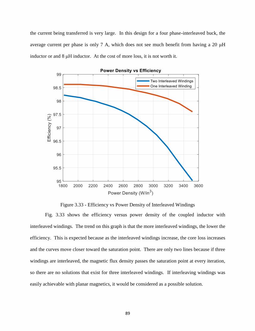
89
the current being transferred is very large. In this design for a four phase-interleaved buck, the
average current per phase is only 7 A, which does not see much benefit from having a 20 μH
inductor or and 8 μH inductor. At the cost of more loss, it is not worth it.
Figure 3.33 - Efficiency vs Power Density of Interleaved Windings
Fig. 3.33 shows the efficiency versus power density of the coupled inductor with
interleaved windings. The trend on this graph is that the more interleaved windings, the lower the
efficiency. This is expected because as the interleaved windings increase, the core loss increases
and the curves move closer toward the saturation point. There are only two lines because if three
windings are interleaved, the magnetic flux density passes the saturation point at every iteration,
so there are no solutions that exist for three interleaved windings. If interleaving windings was
easily achievable with planar magnetics, it would be considered as a possible solution.

90
Figure 3.34 - Power Density vs Efficiency Overall Comparison
Fig. 3.34 shows the power density versus efficiency for all of the previous cases that were
examined. A six turn inductor switched at 400 kHz has the best overall efficiency over most of
the power densities until the inductor starts to become very small, which then it is overtaken by
the six turn inductor switched at 500 kHz. This is expected because as the magnetics get smaller,
the switching frequency needs to increase in order to keep the core loss and magnetic flux density
under saturation. This is not a final determination of which case will be used, but just a summary
of what has been explained.
3.3 Design of Inductors: Two-Phase Coupled Inductor for Two-Phase Buck
The previous section discussed the design of a two-phase coupled inductor for a four phase
interleaved buck converter. The next step in the design process is to investigate another two phase
coupled inductor, but for a two-phase interleaved buck converter. From the previous chapter, there

91
were two topologies that were being considered: the four phase interleaved buck and the two phase
interleaved buck with paralleled devices. Both topologies showed similar device loss
characteristics, so it was worth investigating further.
The design for the coupled inductor will be the same exact process as before. The only
things that change are the average current through each phase of the inductor and the overall size
of the inductor. Instead of splitting the magnetics area in two, the inductor for the two phase
interleaved will have the entire 35 mm width to utilize. The only drawback about this magnetics
design is that the overall height of the converter still needs to be 7 mm, which means that there
will double the amount of current flowing through a similar cross sectional area. It is expected
that the loss for the two-phase design will be higher than the loss for the four-phase design. This
section will not go into the same detail as the previous section. This section will provide more of
the results as all of the concepts and trends are the same as the previous sections.
Figure 3.35 - Loss per Phase for Two-Phase Coupled Inductor
Fig. 3.35 shows the loss per phase for the two-phase coupled inductor. This figure has
been showed before, but the major difference is that the inductor depth being shown is 30 mm, not
22 mm. When the inductor depth is set at 22 mm, there is no useable solution, as each iteration
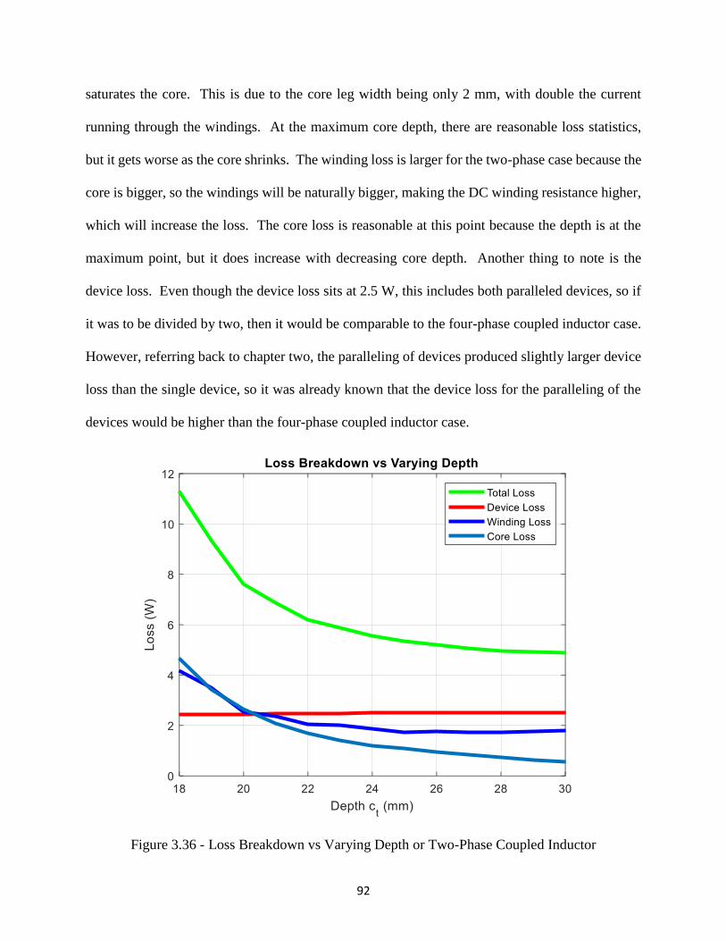
92
saturates the core. This is due to the core leg width being only 2 mm, with double the current
running through the windings. At the maximum core depth, there are reasonable loss statistics,
but it gets worse as the core shrinks. The winding loss is larger for the two-phase case because the
core is bigger, so the windings will be naturally bigger, making the DC winding resistance higher,
which will increase the loss. The core loss is reasonable at this point because the depth is at the
maximum point, but it does increase with decreasing core depth. Another thing to note is the
device loss. Even though the device loss sits at 2.5 W, this includes both paralleled devices, so if
it was to be divided by two, then it would be comparable to the four-phase coupled inductor case.
However, referring back to chapter two, the paralleling of devices produced slightly larger device
loss than the single device, so it was already known that the device loss for the paralleling of the
devices would be higher than the four-phase coupled inductor case.
Figure 3.36 - Loss Breakdown vs Varying Depth or Two-Phase Coupled Inductor

93
Fig. 3.36 shows the loss breakdown versus varying depth of the two-phase coupled
inductor. In this figure, the minimum core depth is 18 mm as compared to 12 mm for the four-
phase coupled inductor case. The reason for stopping at 18 mm inductor depth is that the core is
saturated at every point below that depth. The core loss starts to increase exponentially as the core
gets smaller, which is expected because double the current is running through the windings with
the same cross sectional area. There are still solutions that exist, however they require a larger
area to achieve the same efficiency as the four-phase coupled inductors. The winding loss
increases exponentially because of the low inductance at smaller depths shown in the next figure.
Figure 3.37 - Inductance vs Varying Depth for Two-Phase Coupled Inductor
Fig. 3.37 shows inductance versus varying depth of the inductor. When the core has a
small depth, the most optimal point is only at 800 nH, which produces a large ripple current of 25
A. This means that the peak and valley current is 26.5 A and 1.5 A. This produces a large FR,

94
which in turn will produce a large total winding resistance. As the inductance gets smaller, the
loss will increase for the windings.
Figure 3.38 - Total Loss and Efficiency of vs Size of Two-Phase Inductor
Fig. 3.38 shows the total loss versus inductor depth and the power density versus efficiency
of the two-phase coupled inductor. As the converter gets smaller, the loss starts to increase
exponentially, until the saturation point is reached and no available solution is left. The two-phase
interleaved converter is able to achieve comparable results to the four-phase interleaved converter;
however, it is at the cost of size. This converter only reaches 2600 W/in3, whereas the four-phase
converter can achieve up to 3600 W/in3 at a higher efficiency. If the same footprint is kept for all
cases, this inductor can never compete with a four-phase approach due to the increasing.

95
Figure 3.39 - Power Density vs Efficiency Comparison
Fig. 3.39 shows the power density versus efficiency comparison between the best
candidates from the previous section. As expected, the two-phase interleaved buck converter has
worse efficiency and lower power density than the four-phase interleaved coupled inductors. This
is because the current has doubled in the two-phase coupled inductor while keeping the cross
sectional area the same. If the two-phase solution were to have comparable efficiency to the four-
phase solution, the outer leg widths would need to be increased. However, increasing the outer
leg widths also increases the height of the inductor, which would decrease the power density. A
small increase of 4 mm to the height of the inductor, allowing for a 2 mm increase on all outer
widths, would drop the maximum achievable power density down to 2200 W/in3. While the
efficiency would increase to more comparable and even higher levels than the four-phase solution,
the slight increase in size would drop the power density too low. In this design, the smallest most

96
efficient converter is desirable, so dropping the power density is not acceptable. However, if power
density were not of paramount importance, the slight increase in height to the inductor would make
the two-phase solution viable option.
3.4 Design of Inductors: Normal Inductor for Four-Phase Buck
In the previous two sections, the design for the four-phase and two-phase interleaved buck
converter magnetics was discussed. Both topologies used two-phase coupled inductors, with the
four-phase topology using two sets of coupled inductors. In this section, the design of separate
normal inductors, with no coupling will be discussed. The coupled inductor was chosen for design
because there are added benefits in terms of switching and conduction losses for the overall
converter. It would be fair to make a comparison with a regular inductor to see which one performs
better.
The design for the normal inductors will follow the same process as the coupled inductor
design with some slight changes. The same layout will be used, so the area for the inductors will
be the same. The only difference is that there will need to be four separate inductors that fit in the
same area, which could be tight. There are a couple different cores shapes that could be viable,
another EI shaped core or a UI core. However, with the space allotted, some of the core shapes
could not fit right or would not make sense. The layout would most likely need to be changed to
accommodate the smaller sized inductors.

97
Figure 3.40 - Normal Inductor Layout Example
Fig. 3.40 shows what the initial layout and footprint for the normal inductors would be. In
this case, the four normal inductors will have to fit inside of the same area as the coupled inductors
did. This layout would not considered as the final layout because of the way the inductors are
arranged. The layout would have to be rearranged, but it is easiest to see that the allotted space
for the magnetics is split into four equal sections as shown in the figure above. If the case with
four normal inductor proves to have the best efficiency and power density, then the layout would
need to be shifted where the input bus would be in the middle of the board and the output bus
would be on two separate edges of the board, so that there is symmetry between each power path.
However, the inductor designed for the figure above will have the same area as all of the other
inductors.

98
Figure 3.41 - Normal Inductor Cross Section
Fig. 3.41 shows the cross sectional area of what the normal inductor will look like as well
as the dimensions of each part. As hinted by Fig. 3.40, the core will be and EI core, with a circular
center leg and two rectangular side legs. The center leg is chosen to be a circular shape because
with rounded edges, the flux will more evenly distribute through the center post. When a core has
straight edges and corners, the flux tends to be higher in those areas, so the more roundness that
can be applied to any core will help in lower the core loss. The normal inductor will use similar
variables to that of the coupled inductor, ‘w’ describes the side, top, and bottom legs widths. With
a constant leg width, the optimization becomes simpler with fewer variables. The only difference
between this and the coupled inductor is that ‘m’ now is defined as the diameter of the center post,
since it is circular. Other than that change, every variable is the same as before.

99
Figure 3.42 - Top Cross Section of Normal Inductor
Fig. 3.42 shows the top cross section of the normal inductor. The windings will still use
12 of the 14 layer PCB and will be wrapped around the center leg. The total depth of the core and
windings is described as ‘ct’, and the total width of the inductor is ‘at’. One important factor to
consider when designing a normal inductor with three posts is that the center leg cross sectional
area should be double the area of the side legs described by equation (45). The reason why the
center leg is double the side legs is that when flux is traveling through the core, it will distribute
evenly between each side leg. This means that the flux will be the same for each leg, so the limiting
factor will be whichever leg is the smallest area. This is common practice for all non-coupled
inductor designs because it simplifies the design.

100
𝜋 (𝑚
2)
2= 2 ∗ 𝑤 ∗ 𝑐 (45)
𝑤 = 2𝑚𝑚 (46)
𝐶𝐶𝑙𝑒𝑎𝑟 = 0.508𝑚𝑚 (47)
𝑚 = √8∗𝑤∗𝑐
𝜋 (48)
𝑤𝑤 =𝑎𝑡−2∗𝑤−𝑚−4∗𝐶𝐶𝑙𝑒𝑎𝑟
2 (49)
Equations (46) – (49) describe the fundamental equations that will be used to find the
physical parameters of the normal inductor core. The width of the legs is the same as before and
will not be changed because of the height limitation put on the design. Equation (48) describes
the center post diameter; it is in terms of the side leg width and core depth. This equation must be
kept true at all times in order to keep the side legs fluxes half of the center leg flux. Once equation
(48) is satisfied, then the rest of the core dimensions can be found and the inductance and fluxes
can be derived.
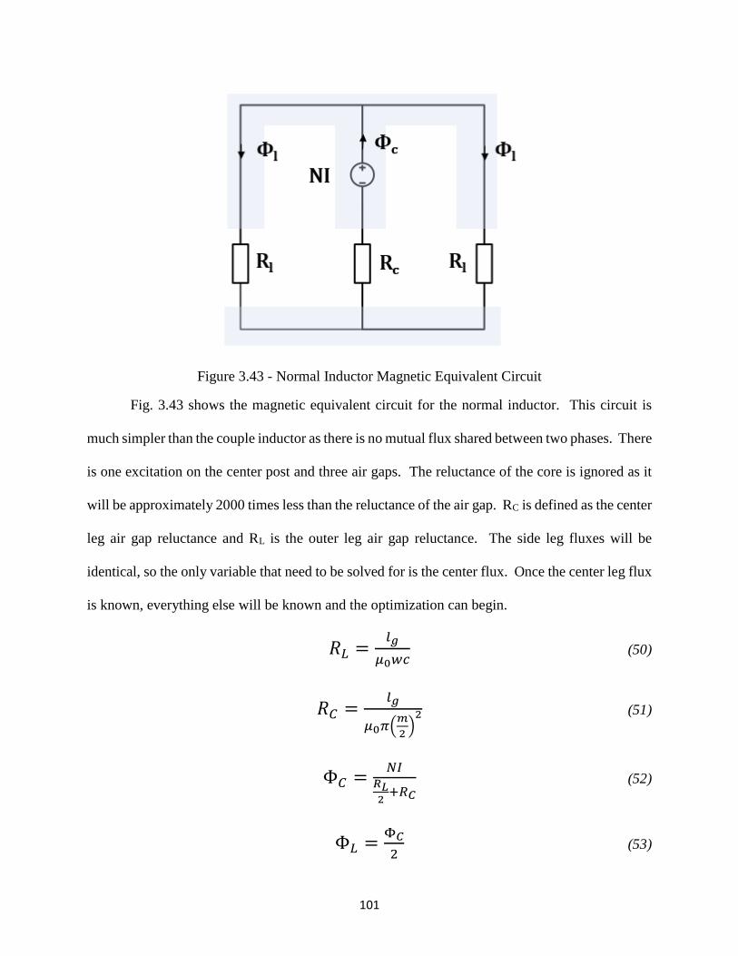
101
Figure 3.43 - Normal Inductor Magnetic Equivalent Circuit
Fig. 3.43 shows the magnetic equivalent circuit for the normal inductor. This circuit is
much simpler than the couple inductor as there is no mutual flux shared between two phases. There
is one excitation on the center post and three air gaps. The reluctance of the core is ignored as it
will be approximately 2000 times less than the reluctance of the air gap. RC is defined as the center
leg air gap reluctance and RL is the outer leg air gap reluctance. The side leg fluxes will be
identical, so the only variable that need to be solved for is the center flux. Once the center leg flux
is known, everything else will be known and the optimization can begin.
𝑅𝐿 =𝑙𝑔
𝜇0𝑤𝑐 (50)
𝑅𝐶 =𝑙𝑔
𝜇0𝜋(𝑚
2)
2 (51)
Φ𝐶 =𝑁𝐼
𝑅𝐿2
+𝑅𝐶
(52)
Φ𝐿 =Φ𝐶
2 (53)
102
𝐿 =𝑁2
𝑅𝐿2
+𝑅𝐶
(54)
Equation (50) – (54) describe the magnetic circuit in Fig. 3.43. This circuit is relatively
easy to solve compared to coupled inductor, which will help with the optimization, as there will
not be as many variables to consider. The only variables that will change in the optimization are
the air gap, core depth, center leg diameter, and turns number. Every other parameter will be
constant and not change throughout the optimization. The inductance is defined by the turns
number squared divided by the total equivalent reluctance, which is shown in equation (54).
The process to define all of the losses in the normal inductor will be the exact same as they
were in the coupled inductor. The total winding loss will be simulated in ANSYS Maxwell and
an equation will be derived from the DC winding resistance. The core loss equation will be similar
to before, but will only have one harmonic, so it will be simpler to calculate.
𝑙𝑤 = 𝜋 ∗ (𝑚 + 2 ∗ 𝐶𝐶𝑙𝑒𝑎𝑟 + 𝑤𝑤) (55)
Equation (55) describes the average winding length for the normal inductor. The winding
path follows a circular path around the center post, so the circumference can be used to calculated
the average length. This equation is then used to calculate the DC winding resistance in equation
(39) from earlier in the coupled inductor section. With the DC winding resistance known, the
scaling factor between DC winding loss and total winding loss can be found.

103
Figure 3.44 - FR Values for the Normal Inductor
Fig. 3.44 shows the simulated curves for the scaling coefficient, FR. Each of the curves
was simulated in ANSYS Maxwell using the same methodology as the coupled inductor. The
results are as expected, the higher the switching frequency, the more winding loss generated due
to the increased eddy current effects. In addition, as the turns number increases, the winding loss
will increase. This is because there are less paralleled winding layer, the closer the turns number
approaches the maximum layers on the PCB. With a six turn inductor, there are two paralleled
layers of copper, where with four turns, there are three paralleled layers, so the winding resistance
will be lower and generate a lower total winding loss. Only FR equations for six turns and four
turns were calculated because when the turns number is decreased to three, the core would saturate
at every point. When the turns number was increased to 12, the winding loss started to dominate
and was not a viable solution.
The core loss is done in almost the exact same way as the coupled inductor, however since
there is no other harmonic in the flux flowing through the core, the core loss equation is much
0
0.1
0.2
0.3
0.4
0.5
0.6
0.7
0.8
0.9
1
0 50 100 150
FR
Ipp2 (A2)
FR at Different Turns and Frequencies
4 Turns 500 kHz
6 Turns 500 kHz
6 Turns 400 kHz

104
simpler. The modified empirical Steinmetz equation that is defined by equation (34) will be used
to calculate the core loss. The magnetic flux density in the core will be purely triangular, so the
same coefficient will be used for each leg.
Figure 3.45 - Magnetic Flux Density for Normal Inductor
Fig. 3.45 shows the magnetic flux density of the center leg and outer legs for the normal
inductor. This was designed with an inductance of 4.5 μH, a core depth of 7 mm, and a center
diameter of 6 mm. There are two lines plotted, however they are exactly the same value. This is
the case because the center post of the inductor is twice the area of one of the outer posts. All the
flux will flow through the center leg and assuming a symmetrical core, half of the center flux will
flow through each separate leg. If half the flux flows through half of the cross sectional area, then
the flux in both the side legs and the center post will be the same. This makes checking for
saturation very easy, if one of the legs is over, then they all will be over and vice-versa.
The same core loss equation used for the coupled inductor can be used as shown in equation
(38). The only difference is that instead of the center leg operating at double the switching
0
0.02
0.04
0.06
0.08
0.1
0.12
0.14
0.16
0.18
0 1 2 3 4
B (
T)
Time (μs)
B-Field
Center Leg
Outer Leg

105
frequency, each leg will operate under the same frequency, so the same scaling factor from before
can be used for every leg. Every loss has now been accounted for in the normal inductor, so an
optimization can be constructed to find the best inductor for the footprint. In the coupled inductor
optimization, there were two variables that were optimized around, the inductance and the
coupling. In the normal inductor, there is no mutual flux, so a different parameter will need to be
swept instead of the center leg. For the normal inductor optimization, the inductance will be swept
as well as the core depth, c. In this case the power density will be swept as the second parameter,
so they plots will be similar to the previous optimization of the coupled inductor.
𝑐𝑡 > 2 ∗ 𝑤𝑤 + 𝑚 + 2 ∗ 𝐶𝐶𝑙𝑒𝑎𝑟 (56)
Equation (56) describes and inequality that must be fulfilled in order to make the inductor
a physically implementable solution. Since the core depth, c, is being swept, at certain core depths,
the size of the windings and center leg will start to exceed the given footprint. Each time the loop
runs, the maximum total inductor depth is set by the user is compared to equation (56). If the core
windings plus center post width is larger than the maximum inductor depth, then the solution is
thrown out and the next loop runs. There is no need to worry about exceeding the size in the a
dimension because the winding width is determined from the total inductor width, so it will always
maximize the winding width to fit in the footprint width-wise.
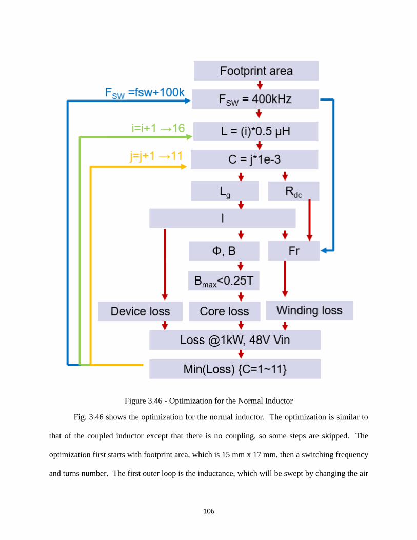
106
Figure 3.46 - Optimization for the Normal Inductor
Fig. 3.46 shows the optimization for the normal inductor. The optimization is similar to
that of the coupled inductor except that there is no coupling, so some steps are skipped. The
optimization first starts with footprint area, which is 15 mm x 17 mm, then a switching frequency
and turns number. The first outer loop is the inductance, which will be swept by changing the air

107
gap. The inner loop is the core depth, which will be swept at each inductance and the most optimal
point will be chosen. With the first parameters set, the air gap can be set to the inductance, which
will allow the current to be calculated. With the calculated current, the peak and valley is known,
so the device loss is now known. In addition to the peak and valley current, the RMS current can
be calculated, which can be used to calculate the winding loss. In addition to device and winding
loss, the core loss can be calculated for each leg based on the peak current. With all three losses
accounted for, they will be summed up and the next iteration of the loop will begin. After each
loop runs, the point that contains the minimum loss will be selected and plotted. In this
optimization, one of the limiting factors is the inductor depth, so if the depth of the core becomes
too large, and then the center post will become too large, which will break the inequality shown
earlier. However, when that inequality is satisfied, the following plots can be produced.
Figure 3.47 - Normal Inductor Loss per Phase
Fig. 3.47 shows the normal inductor loss per phase at an inductor depth of 12 mm. This
plot is similar to what has been shown before, with the plot on the left showing winding and core
loss and the plot on the right shows device, inductor, and total loss. The core loss decreases
steadily as the inductance increases. This is because the core is getting larger and as the core gets

108
larger, the cross sectional area increases, which decreases the reluctance, increasing the
inductance. As the core increases in size, the loss will decrease. In terms of winding loss, the loss
starts out high and settles to an optimal point, and then it starts to increase again. It is very large
at the beginning, so the average length around a single turn is larger so the DC winding resistance
will increase. It starts to increase at very large inductances because the winding width start to
decrease below 1 mm, which will cause the DC winding resistance to rise to a higher value making
the loss greater. There is an optimal point around 7 μH where the winding width and average
length of the winding reach an optimal point. The winding loss dominates the loss, so when the
winding loss is at a minimum, the overall inductor loss will be at a minimum.
Figure 3.48 - Center Post Diameter versus Winding Width
Fig. 3.48 shows the center post diameter width versus the winding width. This plot is
showing that there is a limiting factor in the normal inductor. As one increases the center post

109
diameter the winding width will decrease in diameter. This is because the inductor core width is
fixed on the outer edges by the side legs. The side legs are set to have a 2 mm width no matter
what, so this means that the only two variables that can change are the winding width and the
center post diameter. This also comes into effect when the inductor depth is checked against the
maximum allowed value. The windings and center leg diameter will not be able to increase past
a certain point, unless the entire core is made larger. In order to get a plot of power density versus
efficiency, the core width, at, will need to swept. Sweeping the core width will give a range of
power densities, however some of the larger cases will be well out of the allotted space given to
the magnetics, and those points are shown for completeness.
Figure 3.49 - Power Density vs Efficiency for Normal Inductor
Fig. 3.49 shows the power density versus efficiency for the normal inductor design. This
plot only shows three curves, six turns at different frequencies and a four-turn solution at 500 kHz.

110
The reason why only three curves are plotted is because of the maximum achievable power density.
For all of the cases, they can only achieve up to 2500 W/in3, which is much lower than the cases
for the coupled inductor. The reason why higher power densities cannot be achieve is due to the
width of the inductor limiting the minimum size. The width can be shortened, however the
windings become very small and the winding loss increases exponentially. On top of that, the
magnetic flux density passes the saturation point, so solutions do not exist. However, the
efficiency is just as good and even better than the coupled inductor cases. In order to meet the
power density requirements set by the project specifications, the normal inductor was not
considered due to the increase in size of the magnetic footprint area. If size were not of concern,
the normal inductor would be a better alternative to the coupled inductor.
In this section, a normal EI core inductor with no coupling was investigated. It was shown
how to optimize a core so that the magnetic flux density would be the same through every leg of
the inductor. It was found that the normal non-coupled inductor can achieve very high efficiency,
but sacrifices power density in order to even stay within saturation limit of the core material. If
density is of no concern to the designer, non-coupled inductors is a viable option, however careful
PCB design is required to make sure a symmetrical power loop is utilized. This is the final section
for magnetics design, the upcoming section will compare each design to see what would be most
beneficial for the overall system.
The full MATLAB code that was used to optimize all of the inductors can be found in
Appendix A. This code uses two separate MATLAB files to optimize, one for calculations and
graphs and the other for calculating the air gap given a specific inductance.

111
3.5 Evaluation of Inductors
The previous three sections of chapter three investigated the analysis of different types of
inductors under various conditions. In this section, a brief evaluation of the three separate designs
will be discussed giving the benefits and drawbacks of each design. Each design will be evaluated
by their overall loss, the size of the inductor, and practical implantation onto a printed circuit board.
This is not a standalone buck converter, but a front-end converter to a two-stage bus converter, so
other factors in terms of layout will need to be considered. In addition to an inductor design being
chosen, the switching frequency will also be chosen, which directly influences the loss of the
devices and the overall size of the inductor and converter. Finally, a topology will be chosen
between the four-phase interleaved buck converter and the two-phase interleaved buck converter.
Figure 3.50 - Power Density vs Efficiency for All Designs

112
Fig. 3.50 shows the power density versus efficiency of all the designs that were discussed
in the previous sections. Note that any curve that is not labeled “Normal” will be a coupled
inductor design, while the curves labeled “Normal” are for a non-coupled inductor design. By
using this figure, a design can be chosen based of the peak efficiency or by the smallest design or
something in the middle that deals with a tradeoff between the two. Based on efficiency, the
inductor designs with the best efficiencies are the non-coupled inductors operating at 400 kHz and
500 kHz. However, they only can achieve the best efficiencies when the power density is very
low. Based on power density, most of the coupled inductors can achieve the maximum power
density of 3500 W/in3 before saturation is reached. If deciding on power density alone, the coupled
inductor operating at 500 kHz with six turns would be the best design. Instead of choosing one
design based on either extreme, a more plausible solution would be to choose one where both
power density and efficiency are taken into account.
One issue with choosing a design operating at the maximum power density is that the
magnetic flux density is very close to the saturation point of the core. This means with a limit of
250 mT, each design at the highest power density will be within a couple of mill-Teslas. For this
design, the input voltage is operating at 48V, which means if the input voltage increases to 60V,
then the core will definitely move into saturation. With a larger input voltage, the peak-to-peak
current on the inductor is higher, which will lead to a faster di/dt in the same amount of time. With
the larger di/dt, the magnetic flux density will be higher and the saturation will be reached. One
of the flaws in this design was having the design input voltage at 48V instead of 60V. However,
the chosen design can still be verified to not go into saturation at all input voltages. When choosing
the final design, a point will be chosen that is not at the maximum power density, but one that has

113
a smaller power density and larger efficiency. This can ensure that the inductor will operate in a
safe region over the various input voltages.
Another consideration is that the efficiency does not vary much over most of the designs.
The efficiency change for the normal inductors over varying power densities is almost negligible
because from the maximum to minimum power density, only a 0.3% or 3 W change occurs. This
means that sacrificing a few watts of loss in the buck converter can considerably decrease the size.
This is also true for the coupled inductor until the turns number drop to three. This is due to the
core losses dominating the loss break down at smaller footprint sizes. As one decreases the turns
number, the magnetic flux density increases, so if a smaller turns number is chosen, one would
expect the magnetic flux density to be closer to saturation, meaning that at 60V, the core would
most likely be saturated in steady state.
Based on Fig. 3.50, the only design that can provide higher power density and high
efficiency is a coupled inductor with six turns either operating at 400 kHz or 500 kHz. The
preferred area of the buck converter would be around 3000 W/in3 because it is not too close to the
saturation point and its size is relatively small. The designs only sacrifice a couple of watts, so the
only determination would have to be what switching frequency the converter operates with.
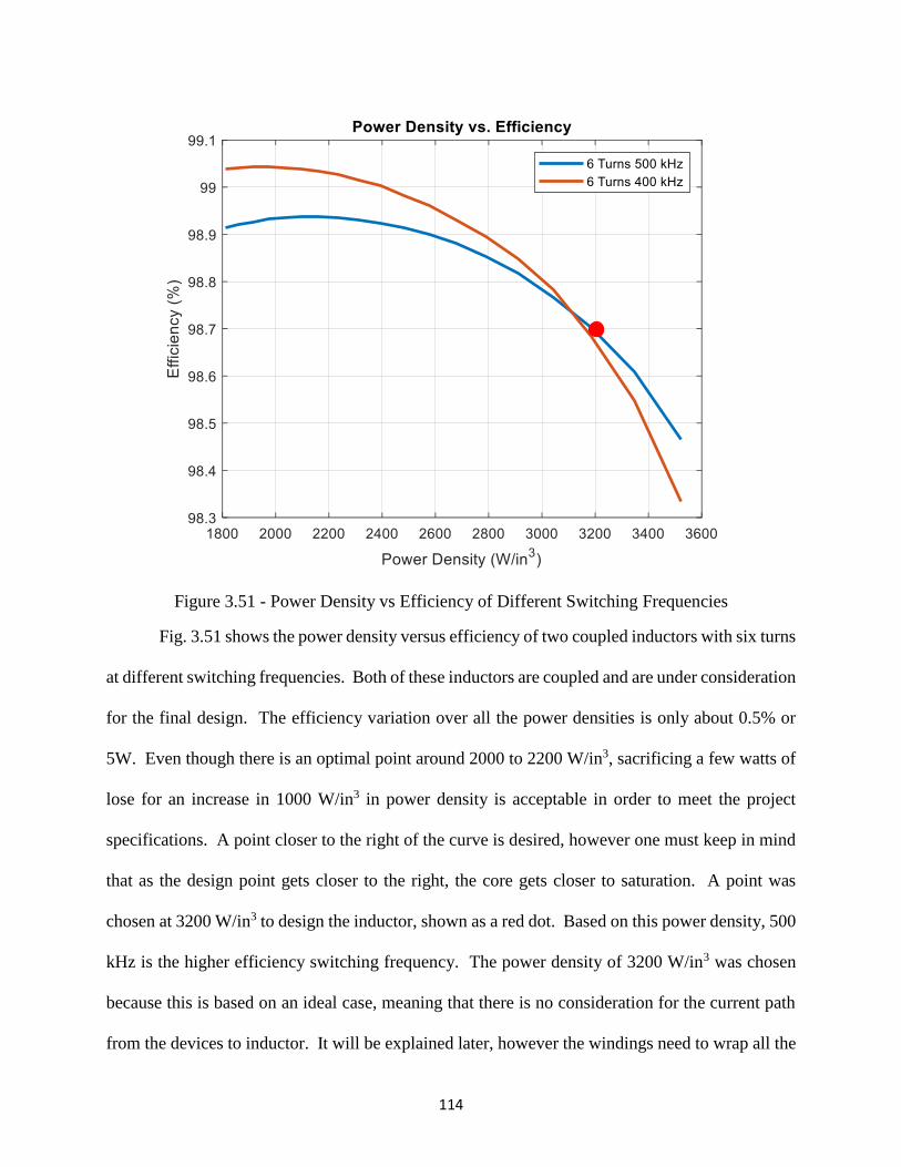
114
Figure 3.51 - Power Density vs Efficiency of Different Switching Frequencies
Fig. 3.51 shows the power density versus efficiency of two coupled inductors with six turns
at different switching frequencies. Both of these inductors are coupled and are under consideration
for the final design. The efficiency variation over all the power densities is only about 0.5% or
5W. Even though there is an optimal point around 2000 to 2200 W/in3, sacrificing a few watts of
lose for an increase in 1000 W/in3 in power density is acceptable in order to meet the project
specifications. A point closer to the right of the curve is desired, however one must keep in mind
that as the design point gets closer to the right, the core gets closer to saturation. A point was
chosen at 3200 W/in3 to design the inductor, shown as a red dot. Based on this power density, 500
kHz is the higher efficiency switching frequency. The power density of 3200 W/in3 was chosen
because this is based on an ideal case, meaning that there is no consideration for the current path
from the devices to inductor. It will be explained later, however the windings need to wrap all the

115
way around the core for one turn, so there will need to be extra space for transitioning between the
switches and inductor. Having a more dense inductor will allow for some leeway when the buck
converter is being layed out.
Another consideration when choosing the switching frequency is the operating frequency
of the LLC. It was predetermined that the LLC would be operating at 1 MHz, so considering EMI
performance, 500 kHz was a better choice because of the buck frequency being on the beat
frequency of the LLC and the equivalent switching frequency (2 MHz) of the buck also being on
the beat. From the analysis from chapter one, 500 kHz was the maximum switching frequency
that could be used without the devices become too hot (>100 °C), so even though the switching
loss will be greater, the core loss at 500 kHz makes up for this when the inductor gets very small.
It was decided that a coupled inductor with six turns operating at 500 kHz would be the design for
the buck converter.
Table 3.2 - Inductor Design Dimensions
Core Width (a) 12.558 mm
Core Depth (c) 9.558 mm
Center Post Width (m) 2.608 mm
Outer Leg Width (w) 2.508 mm
Winding Width (ww) 2 mm
Air Gap (lg) ~200 μm
Total Inductor Width (at) 17.5 mm
Total Inductor Depth (ct) 14.5 mm
Inductance (L) 3.5 μH
Magnetic Material (Ferroxcube) 3F36
Table 3.2 shows the inductor dimensions for the inductor shown in Fig. 3.51. Some of the
dimensions are not round number because of the board clearances that are necessary. There is a
10 mil gap that is necessary between the board and the copper as well as another 10 mill gap that
is needed between the board and the core, which equates to 0.508 mm. This is necessary for any

116
manufacturing errors in either the core or the board. The clearance will allow the core to slide into
the board without any clearance issues. The air gap is approximately 200 μm because Kapton tape
is used for the air gap and to achieve exactly 200 μm is very hard, so it is an approximation. The
thinnest Kapton tape on the market at the time was only 46 μm, so even if five strips of tape were
used for the air gap, an exact calculated inductance would not be able to be achieved, only an
inductance close to the calculated amount. Figures 3.52 to 3.54 shows the front, side, and top view
of the coupled inductor and their dimensions. These schematic were used to order the cores from
Ferroxcube.
Figure 3.52 - Front View of Coupled Inductor

117
Figure 3.53 - Side View of Coupled Inductor
Figure 3.54 - Top View of Coupled Inductor

118
In this section, a comparison of multiple magnetics designs was conducted. It ranged from
a two-phase topology with a single inductor to a four-phase topology that used a coupled inductor
with two core. Normal non-coupled inductors were also evaluated for the four-phase topologies
as a comparison to coupled inductors. After evaluation, it was decided that the operating frequency
for the buck converter would be 500 kHz in a four-phase topology. This topology would utilize
two sets of coupled inductors as the magnetics for the buck. The other magnetic designs proved
to be more beneficial, when converter size is not an issue, but when the density needs to be pushed
as high as possible, coupling the inductors help reduce the magnetic size while keeping the same
performance. In addition, increased the switching frequency helps further push the magnetics to
a smaller size, so that the overall power density of the converter can be larger.
Chapter 4. Control System Design
4.1 Controller Selection
The previous chapters focused on device selection, magnetic design, and the topology for
the buck converter. In this section, the small signal analysis of the buck converter and LLC
converter will be discussed. The control system will included an integrated circuit (IC) that can
be used to control the buck converter and extend to closing the loop around the LLC converter.
The small signal model will be shown and simulated in SIMPLIS software to prove that it can
meet the gain and phase margin requirements of the project.
At the beginning of the project, it was unknown what control method would be used for
the buck converter. It was preferred to use a form of current mode control to limit the current in
each phase; however, the option was open to use an alternative method such as voltage mode
control. Due to the time line of this project, commercial multiphase controllers were taken into
consideration because most controllers on the market have various protection schemes and can

119
operate at a wide range of frequencies and include various other features. The control scheme
could be made with all analog parts, but an IC would be able to implement the same control scheme
in a smaller space.
Figure 4.1 - Multiphase Controller Comparison
Fig. 4.1 shows a sample of the multiphase buck converter controllers that are available on
the market. At the time that the controller survey was done these parts were the best suited for the
application at hand. Some requirements of the controller were that it needed to switch with at least
500 kHz because of the magnetics design from chapter 3. The controller also had to be able to
control four separate phases, if a controller only had two phases, then it needed to be able to be
daisy chained. Having short circuit protection is necessary because if something fails, the
controller needs to be able to react and turn of the converter before there is catastrophic damage.
The controller needs to be able to soft start because when the LLC starts up, if the input voltage

120
slew rate is instant, then there current stress on the switches of the full bridge with be over two that
of full load, which could be damaging. Size is also important because the initial calculations from
chapter 3 did not include the control or auxiliary power supplies, so if the controller can control
four phases and keep a small size it is desirable. Finally, the controller needs to have either voltage
or current mode control for the buck converter.
The ICs that are displayed in Fig. 4.1 are not all viable for this application, but they are
shown for a complete comparison. The LTM4644 and TPS40090 are not suitable for this
application because their IC packages include the MOSFETs inside of the IC so that the only
design that needs to be done is what the output voltage needs to be set at. These controllers are
used for point-of-load (POL) applications that required minimum power, which are usually 12V
to 1V converters. These two controllers would never work with the application that was design in
the earlier sections. The NCP81174 is also another POL converter that can control four-phases,
however the voltage rating on all of the pins is a maximum of 5.5V. This means that any time the
switch node voltage is measured for the over current protection, the voltage will need to be stepped
down, which adds two extra resistors per phase increasing control size and loss. In addition to
that, the VCC voltage is 12V, which means another voltage regulator (VR) would need to be
included with the auxiliary circuits in order to power the controller. Every gate driver on the board
is powered with 5V, so keeping the VCC voltage at 5V is important if space wants to be saved. The
next two controllers, LTC7851 and LTC3861, are the same controllers except that the LTC7851
includes four phase control, while the LTC3861 only includes two phases. This controller is a
viable option, however it is a POL converter, so each time the current is sense for balancing and
over current protection, and it will need to be stepped down. In addition, the LTC7851 is made by
Linear Technologies, so entire converter can be simulated in LTSPICE to see how the part handles
121
at full load and transients. The size is very small, so this controller will be considered for the final
design. As for the LM5170, this controller is a two-phase 48V-12V bi-directional average current
mode controller that is specifically made for the application being designed. Each pin is rated for
100 V, so there is no need to step voltage down, however the switching frequency can only reach
500 kHz and the size is large for one single controller. The VCC voltage is also 12V, so an
additional auxiliary power supply would be needed if this controller were used. However, it does
operate with average current mode, which is preferred because the current is being directly
controlled rather than the voltage, so if there is an overcurrent the control scheme should react
faster than the voltage mode control.
Both the LTC7851 and LM5170 will be considered for controller and both will be analyzed
to see which will perform better. The small signal model will be derived for each control scheme
and whichever performs while keeping in mind implementation on the PCB will be chosen. The
small signal model for the buck converter has already been derived in multiple papers and online
resources, so the focus of this section will be the combination of the buck small signal model with
a coupled inductor and the LLC small signal model. The LLC is operating at the resonant
frequency, so the small signal model can be simplified to an additional LC filter that will be
explained later, making the full closed loop design for voltage mode relatively easy.
4.2 Open Loop Small Signal Analysis
As stated before, the small signal model for the buck converter has already been derived
by many people. This section will focus on implementation and design of the small signal model
for the buck with a coupled inductor and the LLC operating at the resonant frequency. For all
PWM converters, the three terminal model is used to represent the switches in the circuit, both top

122
device and synchronous rectifier. Based on the work done in [21] the three terminal model can be
used for a single-phase buck converter.
Figure 4.2 - Small Signal Model for Single Phase Buck
Fig. 4.2 shows the small signal model for a single-phase buck converter. The three terminal
model is represented by both of the dependent sources and the transform. The sources in lower
case letters represent the small signal parameters and the values in capitalized letters represent the
DC characteristic of the small signal model. The small signal model represents the converter when
small perturbations are introduced into the system, which are represented by the variables
represented in the hats. Everything else in the diagram is standard for a normal buck converter,
with the RL including the resistance from the inductor and the RDSON from the EPC2045.
There is one variable that needs to be changed because coupled inductors are being used in
the circuit instead of non-coupled inductors. As explained in chapter 3, the coupled inductor has
different values for the inductance when operating in steady state and when operating in the small
signal model. The benefit of having a coupled inductor is that the equivalent inductance in the
small signal model is smaller than the self-inductance of each phase. This means that the double
pole caused by the inductor and output capacitor will be pushed to higher frequency, which will
allow the control loop bandwidth to be pushed to a higher frequency. The equations for the
transient inductance and equivalent inductance are as follows [22]:
123
𝐿𝐸𝑄2 = 𝐿 ∗ (1 + 𝛼) (57)
𝐿𝐸𝑄 =𝐿𝐸𝑄2
# 𝑜𝑓 𝑃ℎ𝑎𝑠𝑒𝑠 (58)
𝑅𝐿𝐸𝑄 =𝑅𝐿
# 𝑜𝑓 𝑃ℎ𝑎𝑠𝑒𝑠 (59)
Equations (57) – (59) describe the new parameters of the small signal model. The
equivalent transient inductance is directly related to the coupling coefficient, α. Since the inductors
are inversely coupled, α will be a negative value, making the equivalent inductance smaller than it
already is, which will benefit the closed loop performance. In addition to a smaller transient
inductance, adding more phases to a buck converter will decrease the inductance even further.
Each phase of the buck converter is in parallel with one another, so the impedances are in parallel,
and if each of the self-inductances are identical, then one just needs to divide the equivalent
coupled-inductance by the number of phases as described by (58). This also applies to the series
winding resistance in each inductor. This will further push the control loop bandwidth higher.
However, even though the double pole from the buck converter is pushed to a higher frequency,
there are diminishing returns to pushing the bandwidth higher and higher. Good design practice
for closed loop control in a buck converter is to set the maximum closed loop control bandwidth
at one tenth of the switching frequency. In the case for this converter, that would be at 50 kHz.
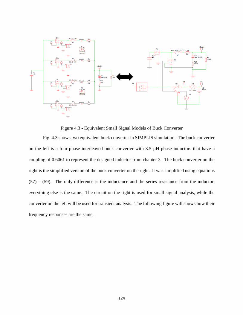
124
Figure 4.3 - Equivalent Small Signal Models of Buck Converter
Fig. 4.3 shows two equivalent buck converter in SIMPLIS simulation. The buck converter
on the left is a four-phase interleaved buck converter with 3.5 μH phase inductors that have a
coupling of 0.6061 to represent the designed inductor from chapter 3. The buck converter on the
right is the simplified version of the buck converter on the right. It was simplified using equations
(57) – (59). The only difference is the inductance and the series resistance from the inductor,
everything else is the same. The circuit on the right is used for small signal analysis, while the
converter on the left will be used for transient analysis. The following figure will shows how their
frequency responses are the same.

125
Figure 4.4 - Frequency Response of Control to Output of the Buck Converter
Fig. 4.4 shows the bode plot of the control-to-output response of the buck converters from
the previous figure. In addition to simulation results, a derived calculation is used for comparison
from [23], which represents the ideal case. The gain plots for each simulation are almost exactly
the same, with slight variation in peaking where the double pole occurs. The damping is caused
by the series resistance in the inductor and the RDSON of the switches. However, the mismatch in
damping is not large, so it will be ignored. On the phase plot, the equivalent buck converter and
the calculation match perfectly, while the four-phase buck with coupled inductors deviates
downward. The rise in the phase is caused by the output capacitor and its series resistance, which
occurs at two decades higher than what is displayed here. The deviation between the four-phase
buck and the simplified buck is caused by in accuracies in the small signal model. The buck is
being switched at 500 kHz, so anything that is above half of the switching frequency (250 kHz) is

126
not an accurate representation of the real converter, which is what the red curve is displaying.
There is a fundament assumption in small signal analysis that higher order terms can be ignored
when doing hand calculations and simplifications. However, as the frequency approaches the
switching frequency, those assumptions are no longer valid and the small signal model does not
work accurately. Anything above 250 kHz will be assumed as inaccurate and will not be
considered because of the fundamental approximations made in PWM converters. Before half of
the switching frequency, the plots match up almost perfectly, so this proves that the model being
used is accurate when it is simplified.
Figure 4.5 - Equivalent Small Signal Model for Interleaved Buck with Coupled Inductor
Fig. 4.5 shows the updated equivalent small signal model for an interleaved buck converter
with coupled inductors. This model will be used when calculating the full control-to-output
transfer function of the entire two-stage converter based off the simulations ran in the previous
figure.
Now that the buck converter small signal analysis has been taken care, the next step is to
find the small signal model for the LLC. Resonant converters operate differently than PWM
converters; they rely on the resonant frequency of the LC tank to control how much energy is
transferred to the load while achieving zero voltage switching (ZVS). The only drawback of
resonant converters is that in order to maintain the output voltage and ZVS across all load

127
conditions the switching frequency needs to change. In certain applications, having a variable
switching frequency is not allowed and in other cases, it is fine. With a variable switching
frequency, the EMI spectrum is very unpredictable and if there are other sensitive converter,
devices, or components on the same application, designing an EMI filter could be extremely
difficult. However, in the case for the two-stage converter, the LLC is operating at the resonant
frequency at all times. The only job for the LLC is to provide isolation for the converter. The
interleaved buck converter will provide regulation for the entire converter. The LLC is basically
a 3:1 transformer, so whatever voltage is provided at its input, it will step it down to three times
the initial value.
This will be extremely beneficial to the design of the closed loop system because all of the
existing models for the LLC are inaccurate when the load deviates or when the switching frequency
changes. With the LLC operating at the resonant frequency all the time, this will simplify its small
signal model to only an equivalent LC filter with some damping.
Figure 4.6 - Circuit Model of the LLC

128
Fig. 4.6 shows the circuit model for the second stage LLC converter. RPrim and RSec
represent the primary and secondary winding resistance respectively. The topology is a 3:1 matrix
transformer with a center-tapped output. The primary side windings are three transformers in
series and the secondary windings are three transformers in parallel with paralleled devices. Each
winding represents a single 1:1 transformer, so with three in series, the primary windings equate
to three transformers in series and the output equates to three 1:1 transformer in parallel, which is
just one winding. This means that the entire transformer for the LLC is a 3:1 voltage ratio. This
structure is too complicated to equate to a small signal model, so it can be simplified into a single
3:1 transformer as shown below.
Figure 4.7 - Equivalent Circuit Model for LLC
Fig. 4.7 shows the equivalent model for the LLC with only one output branch. This model
is exactly the same as the previous circuit model, except some of the values will need to be scaled
because of the simplification. In this converter, the output capacitances of each switch on the
primary and the secondary side all contribute to the operation of the LLC, so they will need to be
included into the small signal model. Their equations are shown below:
𝑅′𝑠𝑒𝑐 =
1
3𝑅𝑠𝑒𝑐 (60)
𝑅′𝐷𝑆𝑂𝑁𝑝 = 2𝑅𝐷𝑆𝑂𝑁𝑝 (61)

129
𝐶′𝑜𝑠𝑠𝑝 =
1
2𝐶𝑜𝑠𝑠𝑝 (62)
𝑅′𝐷𝑆𝑂𝑁𝑠 =
1
6𝑅𝐷𝑆𝑂𝑁𝑠 (63)
𝐶′𝑜𝑠𝑠𝑠 = 6𝐶𝑜𝑠𝑠𝑠 (64)
Equations (60) – (64) represent the RDSON, output capacitances, and secondary winding
resistance of the LLC converter. Equation (60) shows the new equivalent secondary winding
resistance, which is just a third of what it previously was because of the fact that each of the ouput
center taps is in parallel. In normal operation, either Q1 and Q3 or Q2 and Q4 will be on at the
same time, which means that the devices are in series during one-half cycle. This leads to
equations (61) and (62), the resistances are in series, so they add together and the capacitors are in
series, which means they are half of their original value. The Coss is difficult to model in the small
signal domain, so it will be used in the simulation, but will not be modeled for the calculation.
Finally, since there are three paralleled outputs and two devices paralleled, the RDSON of the
secondary side devices will be six times smaller than in the original circuit. As for the
capacitances, since they are in parallel, the become additive, so the Coss of the output capacitances
is six times larger than before. Once again, the Coss is difficult to model in calculation, so it will
be used in the simulation and not the calculation.
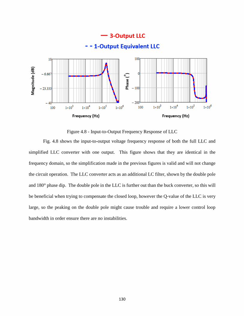
130
Figure 4.8 - Input-to-Output Frequency Response of LLC
Fig. 4.8 shows the input-to-output voltage frequency response of both the full LLC and
simplified LLC converter with one output. This figure shows that they are identical in the
frequency domain, so the simplification made in the previous figures is valid and will not change
the circuit operation. The LLC converter acts as an additional LC filter, shown by the double pole
and 180° phase dip. The double pole in the LLC is further out than the buck converter, so this will
be beneficial when trying to compensate the closed loop, however the Q-value of the LLC is very
large, so the peaking on the double pole might cause trouble and require a lower control loop
bandwidth in order ensure there are no instabilities.
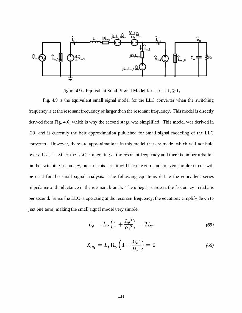
131
Figure 4.9 - Equivalent Small Signal Model for LLC at fs ≥ fo
Fig. 4.9 is the equivalent small signal model for the LLC converter when the switching
frequency is at the resonant frequency or larger than the resonant frequency. This model is directly
derived from Fig. 4.6, which is why the second stage was simplified. This model was derived in
[23] and is currently the best approximation published for small signal modeling of the LLC
converter. However, there are approximations in this model that are made, which will not hold
over all cases. Since the LLC is operating at the resonant frequency and there is no perturbation
on the switching frequency, most of this circuit will become zero and an even simpler circuit will
be used for the small signal analysis. The following equations define the equivalent series
impedance and inductance in the resonant branch. The omegas represent the frequency in radians
per second. Since the LLC is operating at the resonant frequency, the equations simplify down to
just one term, making the small signal model very simple.
𝐿𝑒 = 𝐿𝑟 (1 +Ω𝑜
2
Ω𝑠2) = 2𝐿𝑟 (65)
𝑋𝑒𝑞 = 𝐿𝑟Ω𝑠 (1 −Ω𝑜
2
Ω𝑠2) = 0 (66)

132
Figure 4.10 - Simplified Equivalent Small Signal Model for LLC at fs ≥ fo
Fig. 4.10 shows the simplified equivalent small signal model for the LLC. Since the
frequency is not being perturbed, all of the sources in the LC tank become zero. With the switching
frequency equal to the resonant frequency, the equivalent reactance becomes zero and the
equivalent inductance is just double the original resonant inductance. One major approximation
about this model is the assumption that the magnetizing inductance, Lm, becomes infinite, so that
the branch disappears. The assumption is that the magnetizing inductance does not contribute
anything to the model and can be ignored. When the switching frequency starts to deviate from
the resonant frequency, the magnetizing inductance will start to come into the model and contribute
to various beat frequencies, moving the double pole of the LLC slightly. In the model derived for
the two stage, it is assumed that the magnetizing inductance will not contribute over all load
conditions to simplify analysis. However, this assumption will not hold over all cases, which will
be shown in the simulation verification.
𝐿′𝑒 =
𝜋2𝐿𝑟
4𝑛2 (67)
𝑅𝐿𝐿𝐶 = 𝑅′𝐷𝑆𝑂𝑁𝑝 + 𝑅𝑝𝑟𝑖𝑚 +
8𝑛2
𝜋2(𝑅′
𝐷𝑆𝑂𝑁𝑠 + 𝑅′𝑠𝑒𝑐) (68)
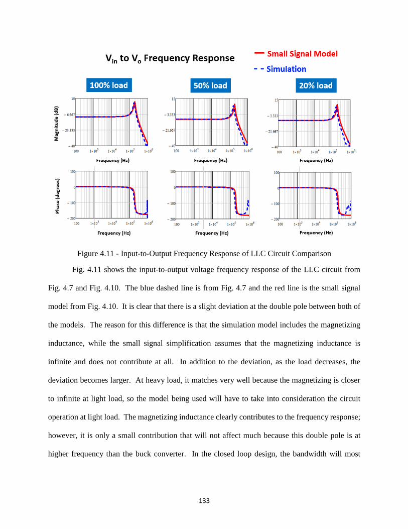
133
Figure 4.11 - Input-to-Output Frequency Response of LLC Circuit Comparison
Fig. 4.11 shows the input-to-output voltage frequency response of the LLC circuit from
Fig. 4.7 and Fig. 4.10. The blue dashed line is from Fig. 4.7 and the red line is the small signal
model from Fig. 4.10. It is clear that there is a slight deviation at the double pole between both of
the models. The reason for this difference is that the simulation model includes the magnetizing
inductance, while the small signal simplification assumes that the magnetizing inductance is
infinite and does not contribute at all. In addition to the deviation, as the load decreases, the
deviation becomes larger. At heavy load, it matches very well because the magnetizing is closer
to infinite at light load, so the model being used will have to take into consideration the circuit
operation at light load. The magnetizing inductance clearly contributes to the frequency response;
however, it is only a small contribution that will not affect much because this double pole is at
higher frequency than the buck converter. In the closed loop design, the bandwidth will most

134
likely be set before the buck double pole to ensure stability, so the slight shift in LLC double pole
should have no impact. The simplification made in Fig. 4.10 will be used for small signal analysis.
Equations (67) and (68) show the values of the final equivalent small signal model from
the LLC. The equivalent inductance is transferred over the transformer and scaled by factor
defined in [24]. RLLC sums all of the series resistance from Fig. 4.5 into one resistance so the
analysis is much simpler. The input perturbation will be ignored on the LLC because it will be
connected directly onto the buck small signal model and from there the control-to-output transfer
function can be derived and assessed for stability.
Figure 4.12 - Two-Stage Small Signal Model
Fig. 4.12 shows the final small signal model for the two-stage converter. The input source
is removed from the LLC model and is replaced by the equivalent buck small signal model. This
model can be used to find the control-to-output transfer function, which will used to assess stability
and controllability of the system. For this project, the audio-susceptibility and input/output
impedances are not of concern, as this is just a standalone design, so the small signal model can
be simplified even further.
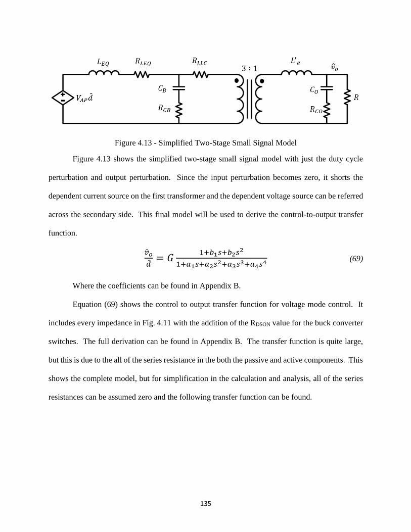
135
Figure 4.13 - Simplified Two-Stage Small Signal Model
Figure 4.13 shows the simplified two-stage small signal model with just the duty cycle
perturbation and output perturbation. Since the input perturbation becomes zero, it shorts the
dependent current source on the first transformer and the dependent voltage source can be referred
across the secondary side. This final model will be used to derive the control-to-output transfer
function.
�̂�𝑜
�̂�= 𝐺
1+𝑏1𝑠+𝑏2𝑠2
1+𝑎1𝑠+𝑎2𝑠2+𝑎3𝑠3+𝑎4𝑠4 (69)
Where the coefficients can be found in Appendix B.
Equation (69) shows the control to output transfer function for voltage mode control. It
includes every impedance in Fig. 4.11 with the addition of the RDSON value for the buck converter
switches. The full derivation can be found in Appendix B. The transfer function is quite large,
but this is due to the all of the series resistance in the both the passive and active components. This
shows the complete model, but for simplification in the calculation and analysis, all of the series
resistances can be assumed zero and the following transfer function can be found.
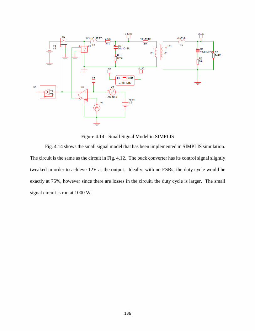
136
Figure 4.14 - Small Signal Model in SIMPLIS
Fig. 4.14 shows the small signal model that has been implemented in SIMPLIS simulation.
The circuit is the same as the circuit in Fig. 4.12. The buck converter has its control signal slightly
tweaked in order to achieve 12V at the output. Ideally, with no ESRs, the duty cycle would be
exactly at 75%, however since there are losses in the circuit, the duty cycle is larger. The small
signal circuit is run at 1000 W.
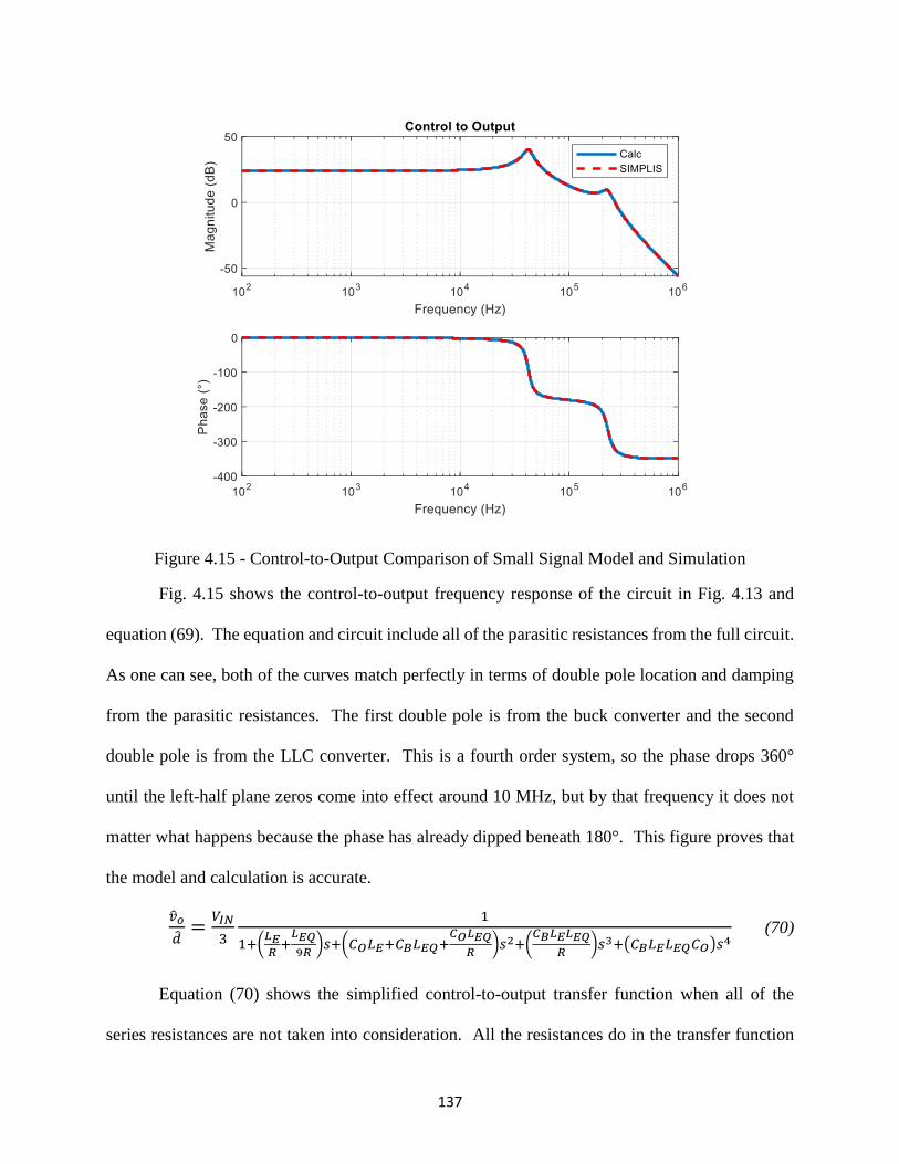
137
Figure 4.15 - Control-to-Output Comparison of Small Signal Model and Simulation
Fig. 4.15 shows the control-to-output frequency response of the circuit in Fig. 4.13 and
equation (69). The equation and circuit include all of the parasitic resistances from the full circuit.
As one can see, both of the curves match perfectly in terms of double pole location and damping
from the parasitic resistances. The first double pole is from the buck converter and the second
double pole is from the LLC converter. This is a fourth order system, so the phase drops 360°
until the left-half plane zeros come into effect around 10 MHz, but by that frequency it does not
matter what happens because the phase has already dipped beneath 180°. This figure proves that
the model and calculation is accurate.
�̂�𝑜
�̂�=
𝑉𝐼𝑁
3
1
1+(𝐿𝐸𝑅
+𝐿𝐸𝑄
9𝑅)𝑠+(𝐶𝑂𝐿𝐸+𝐶𝐵𝐿𝐸𝑄+
𝐶𝑂𝐿𝐸𝑄
𝑅)𝑠2+(
𝐶𝐵𝐿𝐸𝐿𝐸𝑄
𝑅)𝑠3+(𝐶𝐵𝐿𝐸𝐿𝐸𝑄𝐶𝑂)𝑠4
(70)
Equation (70) shows the simplified control-to-output transfer function when all of the
series resistances are not taken into consideration. All the resistances do in the transfer function

138
is damp the resonant frequencies in the circuit. Without them, the poles are still in the same
location, however the peaking is becomes larger. This transfer function is shown just to give an
estimation of how the full transfer function looks. Another change is the zeros of the transfer
function disappear. This is because those zeros are based upon the equivalent series resistance
(ESR) of the capacitors and place zeros at very high frequency, usually around 10 MHz depending
on the ESR and capacitor size. They usually negligible if small capacitances or small ESRs are
used in the circuit.
Figure 4.16 - Small Signal Model with Magnetizing Inductance
Fig. 4.16 shows the small signal model, but now the LLC is using the circuit model from
Fig. 4.7. This model includes the magnetizing inductance, which will verify the deviation of the
LLC double pole.

139
Figure 4.17 - Frequency Response of Control-to-Output of Two-Stage Converter
Fig. 4.17 shows the control-to-output frequency response of the circuit shown in Fig. 4.15.
As expected, the double pole for the LLC is slightly different from the calculation. This is because
the fundamental assumption that the magnetizing inductance is infinite is incorrect. The
magnetizing inductance contributes to the second double pole, making it appear at a lower
frequency. Even though there is this slight deviation, it does not influence the entire frequency
response of the converter. The DC gain and buck converter double pole still match perfectly, so
the is no interaction between the magnetizing inductance and the buck converter. This is beneficial
to the closed loop design, because the closed loop bandwidth will be set lower than the buck double
pole to avoid peaking from the LLC and buck. The calculation and simulation start to deviate
around 400 kHz because of the devices. The buck converter is operating at 500 kHz, so the
fundamental approximation for small signal models stops being valid at 250 kHz, so anything

140
beyond that point cannot be modeled accurately. All of the high frequency terms start to interact
with each other making the model unpredictable. This model is deemed to be acceptable for small
signal design because the deviation in frequency response happens at a higher frequency than what
he control bandwidth will be set at. As long as the double pole form the LLC is well attenuated,
then this model will be suitable.
4.3 Closed Loop Design for Voltage Mode Control
Now that the open loop small signal model has been verified for the two-stage design, the
closed loop can now be designed. For a traditional buck converter a type-III compensator is used
to control the system. From the previous section, the buck converter exhibits a double pole caused
by the LC filter with a relatively large peak. The double pole causes the phase to drop to 180°,
which will not cause the buck to go unstable, but there will be no DC regulation. For a DC-DC
converter, the goal is to have high regulation at DC, so in order to achieve this; an integrator is
needed in the compensator. Adding an integrator means that the gain at DC is infinite, however it
drops the entire phase response by 90°, which will put the converter in an unstable state. In order
to bring the converter out of instability, a type-III compensator is needed.
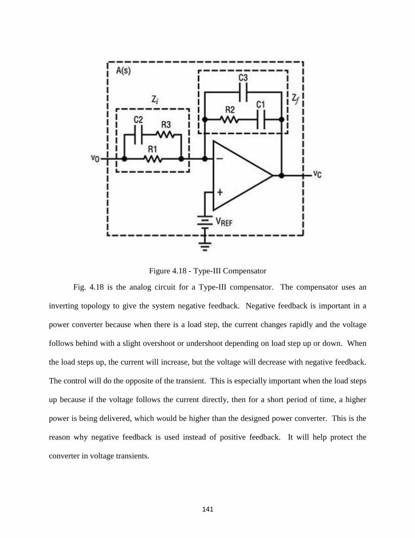
141
Figure 4.18 - Type-III Compensator
Fig. 4.18 is the analog circuit for a Type-III compensator. The compensator uses an
inverting topology to give the system negative feedback. Negative feedback is important in a
power converter because when there is a load step, the current changes rapidly and the voltage
follows behind with a slight overshoot or undershoot depending on load step up or down. When
the load steps up, the current will increase, but the voltage will decrease with negative feedback.
The control will do the opposite of the transient. This is especially important when the load steps
up because if the voltage follows the current directly, then for a short period of time, a higher
power is being delivered, which would be higher than the designed power converter. This is the
reason why negative feedback is used instead of positive feedback. It will help protect the
converter in voltage transients.

142
𝐻(𝑠) = −𝑍𝑓
𝑍𝑖=
(𝑠𝐶2(𝑅1+𝑅3)+1)(𝑠𝐶1𝑅2+1)
(𝑠𝑅1(𝐶1+𝐶3))(𝑠𝐶2𝑅3+1)(𝑠𝑅2𝐶3+1) (71)
Equation (71) describes the transfer function for the type-III compensator at derived in
[25]. The transfer function has a single integrator, two poles, and two zeros. The integrator allows
the gain at DC or 0 Hz to be infinite. The two zeros raise the phase up 180° in order to compensate
the double pole from the buck converter LC filter. Finally, the two poles bring the gain back down
to a stable state. If there are not two high frequency poles, then the gain will not be attenuated
sufficiently to keep high frequency noise (such as switching frequency) out of the control loop.
High frequency noise is unpredictable and it can have large peaking, so making sure there is at
least 40 dB of attenuation is important. The two poles ensure that the gain will keep decreasing
no matter what and there will be no instability from high frequency noise. From the previous
section, it is known that there are two high frequency ESR zeros around 10 MHz, so the two
compensator poles are used to attenuate that them so the gain does not rise up.
𝐼𝑓 𝐶1 ≫ 𝐶3 𝑎𝑛𝑑 𝑅1 ≫ 𝑅3
𝜔𝐼 =1
𝑅1𝐶1 (72)
𝜔𝑧1 =1
𝑅2𝐶1 (73)
𝜔𝑧2 =1
𝑅1𝐶2 (74)
𝜔𝑝1 =1
𝑅3𝐶2 (75)
𝜔𝑝2 =1
𝑅2𝐶3 (76)

143
Equations (72) – (76) describe the poles and zeros of the type-III compensator displayed
in Fig. 4.17. If the statement above the equations is fulfilled with the components being three
orders of magnitude larger, then the poles and zeros can be simplified to simpler equations. As
stated before there is one integrator, two poles, and two zeros, that will be used to give infinite
gain at DC, boost the phase around the buck double pole, and attenuate the high frequency noise.
The design process for the type-III compensator starts by placing the poles and zeros in the open
loop transfer function and then depending on what gain and phase margin is attainable, they can
be adjusted to get the maximum values. A general rule of thumb for designing closed loop systems
for buck converters is that the closed loop bandwidth should be no more than 1/10th of the
switching frequency with a phase margin with at least 45° and gain margin greater than 15 dB.
These general rules help ensure that the converter will be stable over every operating condition
and that high frequency noise will not cause issues.
From the previous section, the open loop control-to-output transfer function was derived
and verified, so using MATLAB, the poles and zeros can be placed and the gain/phase margin will
be updated in real time. MATLAB will also tell the exact location of the poles and zeros, so those
locations can then be used to calculate the values of the compensator components. After the
compensator has be calculated, those values can then be input to the SIMPLIS simulation to test
the transient response and verify that the converter is stable over every operating condition.
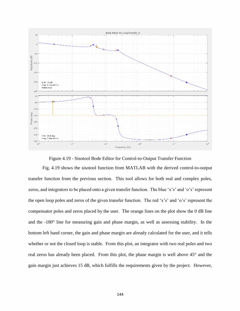
144
Figure 4.19 - Sisotool Bode Editor for Control-to-Output Transfer Function
Fig. 4.19 shows the sisotool function from MATLAB with the derived control-to-output
transfer function from the previous section. This tool allows for both real and complex poles,
zeros, and integrators to be placed onto a given transfer function. The blue ‘x’s’ and ‘o’s’ represent
the open loop poles and zeros of the given transfer function. The red ‘x’s’ and ‘o’s’ represent the
compensator poles and zeros placed by the user. The orange lines on the plot show the 0 dB line
and the -180° line for measuring gain and phase margin, as well as assessing stability. In the
bottom left hand corner, the gain and phase margin are already calculated for the user, and it tells
whether or not the closed loop is stable. From this plot, an integrator with two real poles and two
real zeros has already been placed. From this plot, the phase margin is well above 45° and the
gain margin just achieves 15 dB, which fulfills the requirements given by the project. However,

145
the closed loop bandwidth is only 2.65 kHz, which is quite small for a switching frequency of 500
kHz.
In order to achieve a high gain and phase margin, the closed loop bandwidth needs to cross
before the buck double pole. This is because there is an additional LC filter from the LLC
converter that is at slightly higher frequency than the buck double pole. Typically, for a
conventional buck converter the bandwidth can be set above the double pole, but in this case the
Q-value from the LLC is too large. With a large Q-value, the peaking will rise back above the 0
dB line and cause instability. It can be designed so the bandwidth is above the buck double pole,
but that would require the compensator components to be exactly as designed. That is impossible
in hardware implementation because all components have tolerances and not all designed values
actually have real world components. This means that if a designed value of a capacitor is 300 pF,
the next closest value that can be bought from a supplier is 330 pF. This will shift a designed pole
or zero a couple of kHz, which will change the design of the compensator. In addition to relative
tolerance, the capacitors also behave differently when a voltage is applied to them, so designing
for a specific value is not good design practice. The closed loop bandwidth needs to be designed
lower than the buck double pole to ensure stability over every operating condition.
With the poles and zeros placed in Fig. 4.18, equations (72) – (76) can be used to calculate
the compensator components. Table 4.1 summarizes the compensator calculated component
values and the closest standard values that are available for purchase.

146
Table 4.1 - Compensator Components for Voltage Mode Control
Component Calculated Value Standard Value
R1 10000 Ω 10000 Ω
R2 47 Ω 47 Ω
R3 2247 Ω 2200 Ω
C1 95.2 nF 91 nF
C2 186 pF 180 pF
C3 411 pF 390 pF
With the compensator components calculated, the small signal model can be confirmed
with calculated version. Fig. 4.15 will be used to verify that the calculation matches the small
signal model.
Figure 4.20 - Closed Loop Small Signal Model Comparison

147
Fig. 4.20 shows the comparison of the closed loop calculation and the SIMPLIS simulation.
Once again, the graphs match exactly until the double pole form the LLC is reach. This is due to
the magnetizing inductance having some effect on the LLC double pole. The closed loop is able
to achieve over 90° of phase margin and 30 dB of gain margin with a closed loop bandwidth of
2.85 kHz. This is more than enough to for the system to be stable over every operating conditions.
The only issue that could arise from using voltage mode control is the double pole peaking on the
buck converter. As shown by the bode plot, the double pole peak comes within 3 dB of crossing
back over the unity gain line (0 dB). If this peak is to cross back over 0 dB, then the system would
not be stable and unknown phenomenon would most likely occur during normal operation. It is
expected however that the PCB will have more path resistance that would not be included in the
model, which would damp the system even more, however that is unknown at this time. The gain
of the compensator can be made lower to move the peaking away from instability, however when
the gain is lowered, the closed loop bandwidth will shrink making the whole system slower to
transient responses.
The small signal model has proven to match the circuit, so the next step is to run the
transient analysis to see if the compensator works in normal operation. The full four-phase buck
converter will be used with the simplified single output LLC. All of the parasitic impedances are
used for the LLC converter because they are critical to the circuit operation and achieving ZVS.
The buck converter will only include the two-coupled inductors among four phases. Even though
output signal is crossing over isolation, the circuit will still be simulated, because in simulation
everything is considered ideal. If voltage mode is chosen for the final closed loop control, the
ADuM3190 will be used for the signal to cross isolation [26]. The ADuM3190 is an isolation
amplifier that can transmit analog signals across isolation barriers. It has a bandwidth of 400 kHz,

148
so the pole will be further out than the LLC double pole, which will help attenuate high frequency
noise even further. The only adjustment to the circuit that needs to be made is there is a small
delay in the control of 25 ns. This will not affect the gain of the closed loop, only the phase. It
will start to make the phase oscillate around -180°, but it is much further out that the crossover
frequency, so it does not affect the closed loop at all.
Figure 4.21 - Full Circuit for Transient Analysis
Fig. 4.21 shows the four-phase interleaved buck converter with the LLC converter that will
be used for transient analysis. The inductors for the buck converter have a self-inductance of 3.5
μH and coupling of 0.6061. The bus capacitance is set at 30 μF and the output capacitance is set
at 100 μF. Both of these values are achievable with the given PCB layout. The design guidelines
from Table 1.1 required that the load step from 100% to 50% settle within 50 μs with a current
slew rate of 1 A/μs.

149
Figure 4.22 - Load Step Up
Fig. 4.22 shows the load step up for the full two-stage converter. The output power of the
converter is 1 kW, so the output current at full load would be 83.33 A, which is shown in the figure.
When the load steps, the valley of the output voltage drops to 11.8 V and slowly returns to 12V
before the next transient at 15 ms. From this plot, it looks like the voltage does not settle back,
however the standard rule of thumb for settling time is that once the output voltage comes within
2% of the steady state value, the voltage has settled. In this case with 100 μF on the output, the
voltage never even reach 11.76 V, so the converter is technically always settled. However, this is
a simulation and this cannot be guaranteed when implemented, so that is something that will be
taken into consideration when choosing the closed loop control method.

150
Figure 4.23 - Load Step Down
Fig. 4.23 shows the load step down for the full two-stage converter. The peak output
voltage only reaches 12.17 V, which is already within the 2% settling time, so this waveform is
already considered settled. The output voltage ripple in steady state (not shown) is only 150 mVpp,
which meets the project specifications. The load step down also is within the requirements of the
project, so the designed system for voltage mode control has been proved to work in simulation.
The system that has been designed here will be taken into consideration for the final control loop.
4.4 Average Current Mode Control Analysis
The previous section focused on the small signal analysis for voltage mode control, which
would be used with the LTC-7851. From section 4.1, it was explained that two separate control
methods would be researched. The second control method is average current mode control, which
is utilized by the LM-5170 from TI [27]. This section will focus of the design of the closed loop

151
system around the LM-5170. The analysis will be not as in depth as the previous section because
TI provides a design tool that can be used to calculate every value for each compensator. TI does
not reveal every internal component to their ICs, they only show the large block diagrams. Based
on the information given in the datasheet and their design calculator, a small signal model can be
made to match closely to their design calculator. This will be used to show some proof that the
model used by TI is accurate to the circuit and show transient results.
The controller under analysis from TI is the LM-5170. This controller is a 48V/12V bi-
directional average current mode controller, meaning that it can transfer power from 48V to 12V
using a buck converter and it can also transfer power from 12V to 48V using the same buck
converter only backwards. A backwards buck converter is simply a boost converter, so energy can
be transferred easily in the opposite direction. However, since the application under analysis is
stepping down voltage, only buck mode will be used.
One of the benefits to using the LM-5170 over the LTC-7851 is that all of the pins are rated
for 100 V, so no signal will need to be stepped down for the controller to handle them. The LTC-
7851 is for controlling a POL converter, while the LM-5170 is designed for controlling 48V/12V
application, which is exactly what this project is. The LM-5170 takes more space than the LTC-
7851 and requires more components, which will require more space, but the LTC-7851 will need
to step down the voltage for the current sensing circuit. In the following paragraphs, there are
benefits and drawbacks to each transient response.

152
Figure 4.24 - Current Loop for LM-5170
Fig. 4.24 shows the current loop for the LM-5170. This loop is very similar to peak current
mode control, however there is no external ramp that is used to compare to the peak inductor
current. In this circuit, a differential amplifier is used to sense the inductor current across a sense
resistor, RCS, which is typically the same in peak current mode control. The main difference is
that a transconductance amplifier is used to compare the voltage control signal and the current
signal instead of a standard operational amplifier. A transconductance amplifier is a voltage
controlled current source and in this case, the gain is fixed. With a current source, the compensator
can be put connected from the output to ground instead of across the device like an operational
amplifier. This is the main difference between peak current mode control and average current
mode control, the transconductance amplifier, at a very high level, acts as a low pass filter. Since
the gain is fixed on the transconductance amplifier, the cutoff frequency does not change, so it will
filter out the ripple of the sensed inductor current and leave a DC value. This DC value is the
average value of the sensed signal and leads to average current mode control. Another benefit of

153
the transconductance amplifier is that it can compare two separate time varying signals unlike an
operational amplifier. An operational amplifier compares one time varying signal to a reference
and in this case, if an operational amplifier was used, more circuitry would be needed to add an
additional low pass filter after the differential amplifier. However, transconductance amplifiers
typically have lower open loop gain operational amplifier, so closed loop design could be a
problem if a low gain transconductance amplifier is used.
The rest of Fig. 4.23 is standard, there is a ramp generator used to generate the duty cycle
from the input voltage. This controller used a fixed gain, KFF, to converter the input voltage to a
peak-to-peak ramp generator. The ramp will change when the input voltage is changed from low
line to high line, however this does not change closed loop too much as ramp peak-to-peak voltage
does not deviate much from the nominal voltage. The DIR pins on the diagram represent whether
or not converter is operating in buck or boost mode, in this case, the DIR pins will always be in
buck mode. The ISETA pin represents control signal coming from the voltage loop, this will be
used to regulate the output voltage.
The last part of diagram is the power stage inductor, Lm. This controller has a separate
current loop for each phase, so the power inductor represents the phase inductance. In the case for
the buck converter that was designed, a coupled inductor was used, so the actual inductance needs
to be changed. From the previous section, the transient inductance has already been derived in
equation (57), which will be used for the design of this control loop. The high and low voltage
port values are just used for an example, this controller can have a maximum input voltage of 85V
and output voltage of 60V.

154
Figure 4.25 - Closed Voltage Loop for LM-5170
Fig. 4.25 shows the full closed loop for the LM-5170. In this circuit, an additional
operation amplifier is added in order to control the output voltage. This outer loop ensures that
the output voltage stays constant at 12V at all times. For that reason, an operational amplifier with
a constant reference that is set by the user is used to compensate the output voltage. The
operational amplifier is not part of the controller chip, so it much be supplied by the designer. For
this design, the OPA-197 from TI was used for the voltage loop operational amplifier. It is a high
bandwidth (10 MHz) and high precision amplifier with high noise immunity. It is important to
have a high bandwidth operation amplifier so that the output can be compensated over every
operating condition. The OPA-197 is powered with the same supply voltage (12V) as the LM-
5170, so there is no need to add an extra power supply, which will help save space on the board.
Another benefit of average current mode control is that the inner current loop gain only has
one pole from the power inductor. With only one pole, the compensator only needs to be type-II,

155
with an integrator, zero, and pole. This is one benefit over voltage mode control because the design
of the control loop is easier. In terms of the buck converter, the voltage loop only adds one more
pole from output capacitor, so only a type-II compensator is needed compensate the output voltage
loop. However, this design has an extra LC filter after the output of the buck converter, which
adds an additional double pole to the transfer function. This could prove to be troublesome if the
double pole of the LLC was at lower frequency; however, in this case, the double pole form the
LLC occurs around 230 kHz as shown in simulation. With the double pole from the LLC being at
that high of frequency, the LLC can be ignored and the closed loop can be controlled around the
buck converter if the closed loop bandwidth is set low enough so the poles and zeros do not
interfere with the LLC. This will simplify the small signal analysis, so that only the buck converter
needs to be analyzed and designed around.
With this assumption being made, no new analysis needs to be done on the buck converter.
TI already provides a design sheet that calculated everything for the user [29]. The only inputs
that are needed for this sheet are the input voltage, output voltage, number of phases, output power,
the power inductor and capacitor value, and the value of the sense resistor used. With these values,
the sheet calculates what the current loop and voltage loop are and recommends values for the
compensator based on general closed loop designs. The compensator values can be changed to
have a faster or slower transient response depending on what the user wants.

156
Figure 4.26 - Small Signal Model for LM-5170
Fig. 4.26 shows the small signal model for the LM-5170. This model is not given by TI, it
was made based upon the block diagram and small signal section from the datasheet [27]. TI
provides the final closed loop result bode plot for both voltage and current mode control, but they
do not provide anything that would give the final closed voltage loop transfer function. The idea
is that if the model can be matched in SIMPLIS with the model given by TI in their design sheet,
then it can be assumed that the closed loop works. If it matches, then the model can be applied to
the full two-stage converter and the final transient can be shown. One difference between this
circuit and the circuit in Fig. 4.24 is that there is a 1V offset internal to the controller that is shown
in a different block diagram. It has little to no effect on the closed loop result, however since TI
has it in their block diagram it will be included.

157
Table 4.2 - Compensator Components for Current and Voltage Loop
Components Current Loop Voltage Loop
RCOMP 820 Ω 2000 Ω
CCOMP 68 nF 15 nF
CHF 680 pF 470 pF
Table 4.2 shows the calculated component values for the current and voltage loop for the
LM-5170. The values were calculated with the TI design tool for this controller. The component
names refer to Fig. 4.23, the voltage and current compensators are the same, so the components
have the same names. In this case, the current loop was designed with a bandwidth of 30 kHz and
the voltage loop was designed with a bandwidth of 2 kHz. Generally, the current loop bandwidth
should be one decade smaller than the switching frequency and the voltage loop should be another
decade smaller than the current loop. In this case the voltage loop was slowed down a little bit to
ensure stability for hardware testing, but it can be increased to around 8 kHz before the component
values start to not be achievable.

158
Figure 4.27 - Bode Plot of Closed Voltage Loop for LM-5170 Design Sheet
Fig. 4.27 shows the bode plot generated by the LM-5170 design sheet provided by TI.
From this plot, lines were drawn to measure the gain and phase margin. The gain margin is
measured when the phase margin hits 0° and the phase margin is measured when the gain hits 0
dB. From this plot it can be difficult know exactly what each value is because TI does not allow
any editing to the sheet. From inspection, the phase margin looks to be around 60° and the phase
margin looks to be just over 20 dB. The scale is very large, so knowing the exact value is difficult.
The bandwidth or crossover frequency is at 2 kHz. This plot will be used to compare to the
SIMPLIS simulation in Fig. 4.25 to see if the models match.

159
Figure 4.28 - Bode Plot of Closed Voltage Loop with SIMPLIS Circuit
Fig. 4.28 shows the bode plot of the circuit shown in Fig. 4.26. From first glance, the bode
plot of the SIMPLIS simulation and the TI design sheet look very similar. SIMPLIS gives the
exact gain and phase margin, which are 24.4 dB and 64° respectively, with a crossover frequency
of 1.88 kHz. Compared to the design sheet, they margins match pretty well with a slight
discrepancy of the crossover frequency. This is due to a pole being slightly different in the
SIMPLIS circuit from the design sheet. It is a minor discrepancy that should not change the overall
operation of the circuit, so the model in SIMPLIS should be an accurate representation of the
design sheet transfer function.
With an equivalent circuit model for the buck converter, the initial assumption of the LLC
double pole can be revisited. The original assumption was that if the LLC double pole is far
enough out that it will not cause issues when the voltage loop is closed around it. The LLC double

160
pole is located around 230 kHz, which corresponds to -40 dB of gain for the closed loop around
the buck converter. The LLC peaking is not as large as the buck converter, so it should not cause
any problems if the voltage loop is closed around it. With this assumption, the closed loop will be
redesigned for the two-stage solution to have a faster voltage loop.
Figure 4.29 - Two-Stage Closed Voltage Loop with Average Current Mode Control
Fig. 4.29 shows the two-stage circuit in SIMPLIS using average current mode control. It
is the same exact circuit used in Fig. 4.20 except now the buck converter is being controlled with
average current mode control. Once again, all of the parasitic impedances are included with the
LLC because they are essential if ZVS is to be achieved. The major difference between this circuit
and the voltage mode circuit is that the bus capacitance has been changed to 12 μF to push the
buck double pole out to a higher frequency while maintaining a reasonable ripple on the bus. The
output capacitance is still at 100 μF.
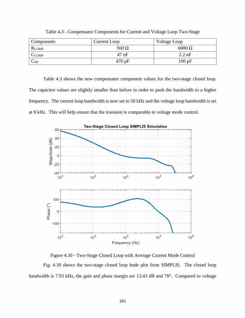
161
Table 4.3 - Compensator Components for Current and Voltage Loop Two-Stage
Components Current Loop Voltage Loop
RCOMP 560 Ω 6000 Ω
CCOMP 47 nF 2.2 nF
CHF 470 pF 100 pF
Table 4.3 shows the new compensator component values for the two-stage closed loop.
The capacitor values are slightly smaller than before in order to push the bandwidth to a higher
frequency. The current loop bandwidth is now set to 50 kHz and the voltage loop bandwidth is set
at 8 kHz. This will help ensure that the transient is comparable to voltage mode control.
Figure 4.30 - Two-Stage Closed Loop with Average Current Mode Control
Fig. 4.30 shows the two-stage closed loop bode plot from SIMPLIS. The closed loop
bandwidth is 7.93 kHz, the gain and phase margin are 13.43 dB and 78°. Compared to voltage
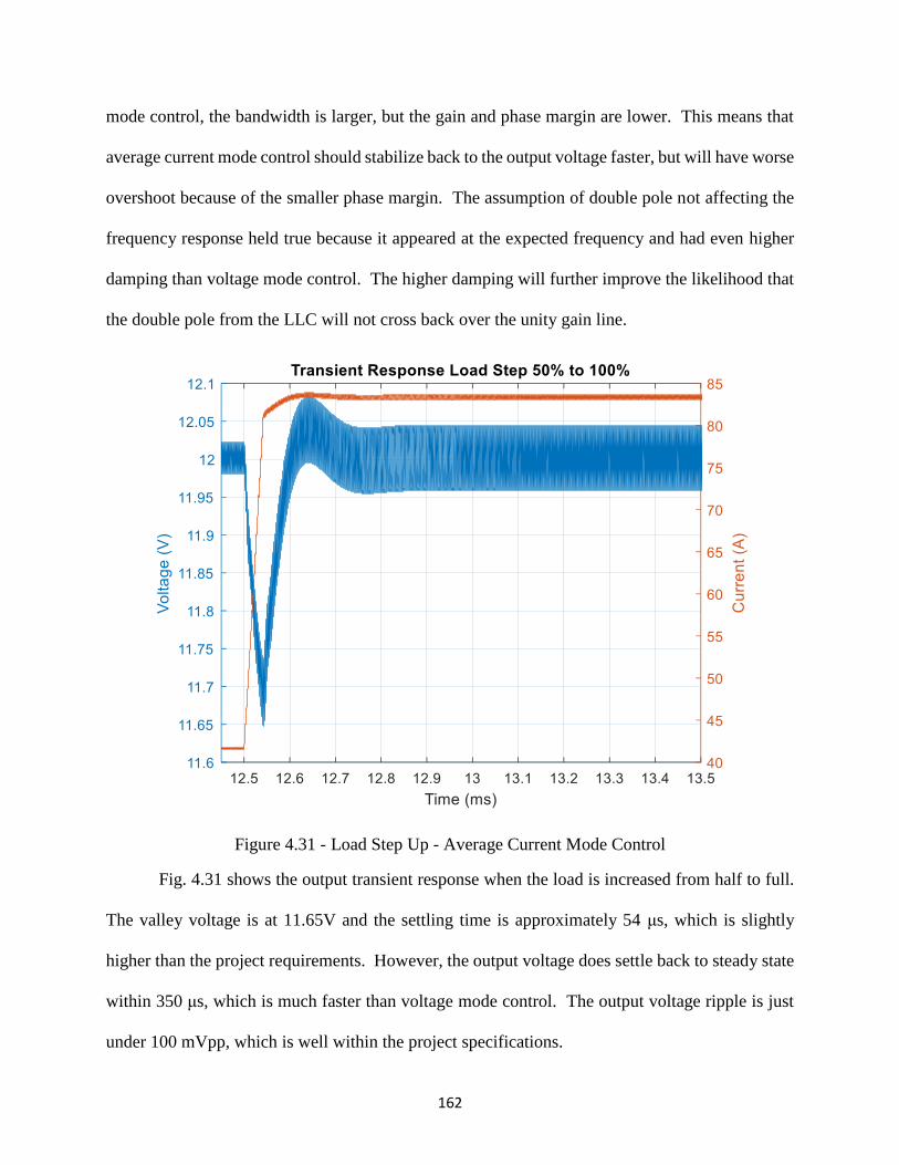
162
mode control, the bandwidth is larger, but the gain and phase margin are lower. This means that
average current mode control should stabilize back to the output voltage faster, but will have worse
overshoot because of the smaller phase margin. The assumption of double pole not affecting the
frequency response held true because it appeared at the expected frequency and had even higher
damping than voltage mode control. The higher damping will further improve the likelihood that
the double pole from the LLC will not cross back over the unity gain line.
Figure 4.31 - Load Step Up - Average Current Mode Control
Fig. 4.31 shows the output transient response when the load is increased from half to full.
The valley voltage is at 11.65V and the settling time is approximately 54 μs, which is slightly
higher than the project requirements. However, the output voltage does settle back to steady state
within 350 μs, which is much faster than voltage mode control. The output voltage ripple is just
under 100 mVpp, which is well within the project specifications.
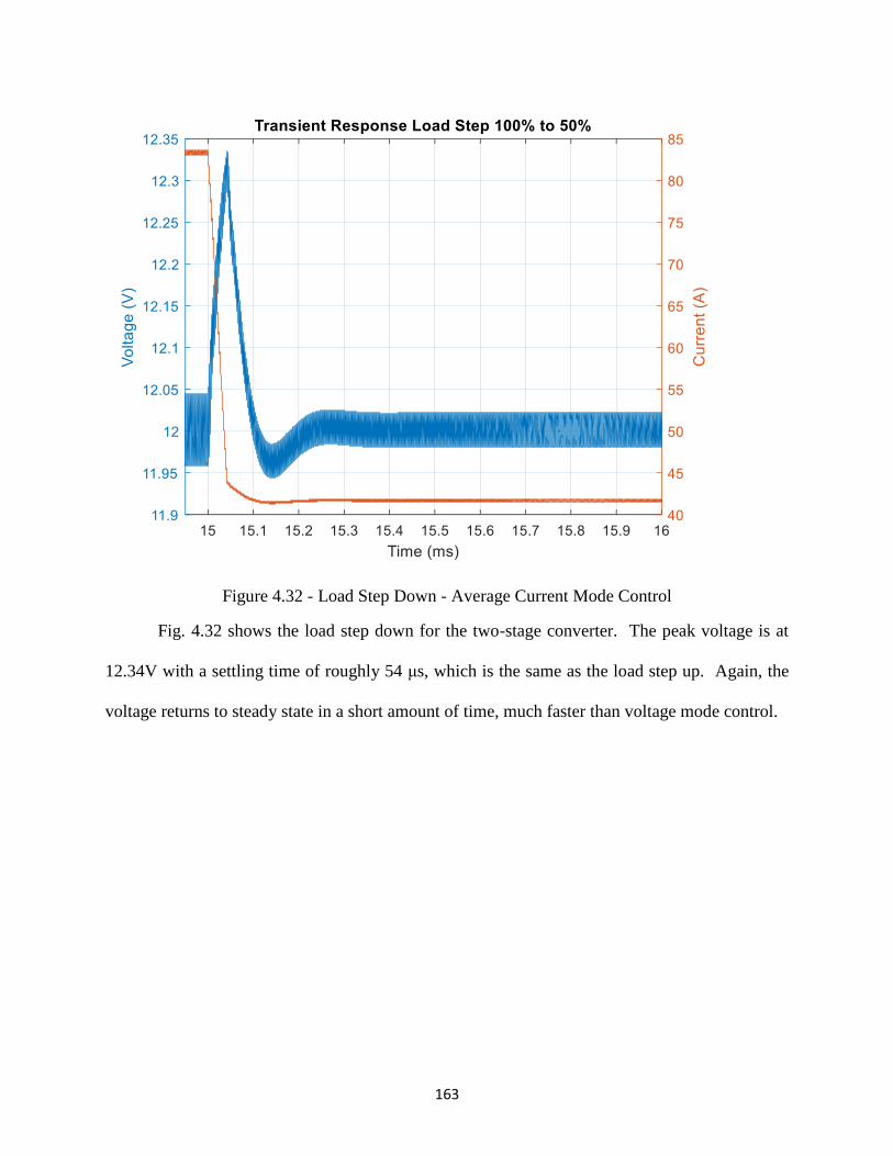
163
Figure 4.32 - Load Step Down - Average Current Mode Control
Fig. 4.32 shows the load step down for the two-stage converter. The peak voltage is at
12.34V with a settling time of roughly 54 μs, which is the same as the load step up. Again, the
voltage returns to steady state in a short amount of time, much faster than voltage mode control.

164
Figure 4.33 - Control Signals for Average Current Mode Control
Fig. 4.33 shows the control signals for average current mode control. The first graph is the
output of the differential amplifier, the second graph is the output of the voltage loop, and the third
graph is the output voltage. The reason for the abrupt decrease in output voltage is due to inner
current loop. Since the current loop has a bandwidth of 50 kHz and the voltage loop has a
bandwidth of 8 kHz, the current loop will work faster than the voltage loop. The transient starts
at 2 ms and shortly after the current reaches steady state at 2.05 ms. At that point, the voltage loop
then takes control and picks up the slack bringing the output voltage to steady state where it finally
settles at 2.25 ms. The most inner loop will always be the fastest, with each subsequent loop going
outward getting slower. The fastest speed will always be limited by the outermost loop.

165
4.5 Control Method Comparison and Selection
The previous two sections analyzed the small signal models for voltage mode control and
average current mode control. Both models were derived and verified with SIMPLIS simulation.
These two forms of control were derived because two controllers were under consideration; the
LTC-7851 and the LM-5170. The LTC-7851 is a voltage mode controller for POL applications
and the LM-5170 is a bi-directional 48V/12V controller that uses average current mode control.
This section will include a comparison between the two control methods and highlight some of the
features of each controller. Then a decision will be made as to which controller will be used for
the two-stage converter.
Figure 4.34 - Comparison of Transient between Voltage and Current Control
Fig. 4.34 shows comparison of voltage mode control and average current mode control
during the load step up. At first glance, average current mode control has higher peaking, but

166
faster settling to steady state than voltage mode control. Average current mode control has a
smaller steady state ripple than voltage mode control. The only benefit that voltage mode control
has over average current mode control is that it settles faster by definition. If the one looks at the
output voltage relatively, voltage mode control does not reach steady state before the next
transient. The only reason why voltage mode is able to meet the settling time is that the phase
margin is over 90°, which is almost 20° higher than average current mode control. The higher the
phase margin, the lower the peaking on the output voltage during transients.
Table 4.4 - Closed Loop Characteristic Comparison
Voltage Mode Average Current Mode
Gain Margin 31.8 dB 13.43 dB
Phase Margin 95° 78°
Settling Time - 54 μs
Closed Loop Bandwidth 2.8 kHz 8 kHz
Table 4.4 shows the comparison of the closed loop between voltage mode control and
average current mode control. By just looking at the numbers, voltage mode control is better in
every aspect other than closed loop bandwidth. However, looking more closely at the closed loop
bode plots and transients; average current mode control has its benefits. In terms of the frequency
response, voltage mode control can achieve a low bandwidth at the cost of marginal stability. The
peaking from double pole on the buck converter is only 3 dB from crossing unity gain and
becoming unstable. If there are any differences between the small signal model and the actual
hardware, then the converter has potential of becoming unstable. This can be fixed by lowering
the gain of the closed loop, however this will drop the bandwidth to a point where it is below 500
Hz and is too small to for converter to respond in a reasonable amount of time. The other issue is
that even though the voltage overshoot/undershoot does not leave the 2% region, it still takes an
upwards of 4 ms to achieve a relative steady state to average current mode control as shown in the

167
previous figure. The only drawback to average current mode control is that the response is slightly
slower than voltage mode control. Overall, the design for average current mode control allows for
more margin of error when constructing the hardware. Voltage mode control requires precise
component values and no deviations from small signal analysis. Some parasitics cannot be avoided
in the PCB layout; they can be minimized but not avoided all together. Since this is a four-phase
interleaved buck converter operating at high switching frequency and moderate input voltage, the
noise from the switching nodes will be at 2 MHz and resonant throughout the board. Average
current mode control does have more noise immunity due to the inherent low pass filters in each
current loop.
Both controllers offer the same features as each other. Both controllers have soft start,
short circuit protection, current balancing, and dead-time selection. The LTC-7851 is a four-phase
controller, so only one chip is needed, whereas the LM-5170 is a two-phase controller, so two will
be need to control the converter. The LM-5170 requires a sensing resistor for current and the LTC-
7851 can use a sensing resistor or the DCR of the inductor. In either case for both controllers,
extra components will be used. In terms of space, the LM-5170 will take up more space than the
LTC-7851. The LTC-7851 is a POL converter so all of the sensed voltages will need resistor
dividers on both the high and low side, which will increase the amount of components. In contrast,
the LM-5170 is specifically designed for this application and able to handle all of the sensed
voltages.
After analyzing both control schemes and controllers, the LM-5170 is controller that will
be used for the two-stage converter. It is specifically designed for applications like this and will
not require voltages to be changed in order to make the controller work. There is some sacrifice
relative to transient response, but the slight increase in settling time is made up for with smaller

168
steady state ripple and faster settling to steady state. The PCB layout will be made with the
consideration that the LM-5170 as the controller for the two-stage converter.
Chapter 5. Prototype Design and Construction
5.1 Circuit Layout
The previous chapters focused on design and verification of the buck converter in
calculation and simulation. This chapter focuses on the design of the prototype hardware of the
buck converter and controller. The layout of the LLC is not discussed in this work, it will be shown
that it is a block on the PCB and it cannot be interfered with. The LLC, buck, and controller will
have an allotted amount of space on the PCB, so each will be layed out separately in their own
sections. After each section is finished, they will be combined onto one board to have a full two-
stage converter.
Before each stage of the converter was layed out, the power flow for the entire circuit
needed to be defined. The board needs to be layed out in a way so that there are not large areas of
coppers that are conducting high amounts of current for no reason. The big issue is connected the
output of the buck converter to the input of the LLC because the space between them is just copper
that will add to conduction losses. Keeping the buck output and LLC input close together is
important when designing the layout for the entire board. In addition to minimizing the space
between the buck and LLC, a linear power flow is desirable in order to keep the isolated output
away from the input. For example, if the input voltage comes from the top side of the board, then
the output should be taken from the bottom of the board, which means the power flows from top
to bottom.

169
Figure 5.1 - Preliminary Two-Stage Layout
Fig. 5.1 shows the preliminary layout for the two-stage converter. The black arrows
indicate the way the power flows through the circuit. The input voltage is at the top of the converter
where the buck is; then it flows down and goes around the inductor. In order for an inductor to
experience a full turn, the winding must flow in a circle around the core, so that is why both the
power leaves and enters the inductor at the same place. Then the output of the buck converter

170
comes down to the left to the LLC full bridge, where the DC signal is made into an AC signal.
Then the power flows around the primary side of the transformer and to ground. Then the output
of the secondary side of the transformer flows straight down completing the power flow. The
control and auxiliary power supplies are all placed in the same location in the top left of the board.
It is important to keep all of the analog signals together and separate from the power flow in order
to avoid noise. However, the gate signal for the buck converter will need to cross the power plane
to reach the gate drive, which will be explained later. It is very important for the LLC gate signals
to be close to each other because many of the devices are paralleled, so the gate signals need to be
exactly the same to ensure that current is split evenly between the paralleled devices. Having all
the housekeeping supplies and controller in the top left location would ensure a small distance for
gate signals for both the buck and LLC.
From the preliminary layout, it was estimated that the size of the converter would be 61mm
x 60mm x 7mm. This means that in order to meet the specification of 550 W/in3, the converter
would only need to operate with 86% efficiency. This is a terrible efficiency for a bus converter
and the project specifications require at least 95% efficiency. If the converter reaches the project
specifications efficiency, then the converter is expected to reach at least 600 W/in3. The results
will be shown in a later chapter; however, this is just a rough calculation to see whether or not the
project specifications are obtainable with the current layout. From the rough calculation, the two-
stage should meet the project specifications, so the layout was started with Fig. 5.1 in mind.
5.2 Gate Driver Layout
The previous section focused on the two-stage layout and the general location of how
everything will be placed on the board. This section and future sections will focus specifically
focus on the buck converter and how different parts will be layed out on the PCB. This section
171
will focus specifically on the gate driver layout for each phase of the buck converter. Gate driver
layout is extremely important for any application because the loop inductance needs to be
minimized or the loss will increase during a switching event.
Figure 5.2 - Optimal Loop for GaN Devices
Fig. 5.2 shows the optimal layout for GaN devices [10]. Parasitic inductances in both the
power and gate loop can add unnecessary loss to any converter that uses a half bridge
configuration. In order to achieve the lowest possible inductance, the power path needs to be as
small as possible. In [10], multiple layouts are tested and the one pictured in Fig. 5.2 proved to be
twice as good as traditional half bridge layouts. In this optimal loop, the input voltage comes from
the top of the board and flows into the input capacitors, and then it flows through the top device
and synchronous rectifier. The most important part is that when the power flows back to the input
source, it takes the shortest path possible. The shortest path possible is to go down one layer and
directly connect that ground layer back to the input capacitor. As shown by the figure on the right,
vias take the ground signal down to layer two and then that layer is directly connected back to the
input capacitor. This layout can achieve less than 500 pH of parasitic inductance, which will
reduce the ringing tremendously.
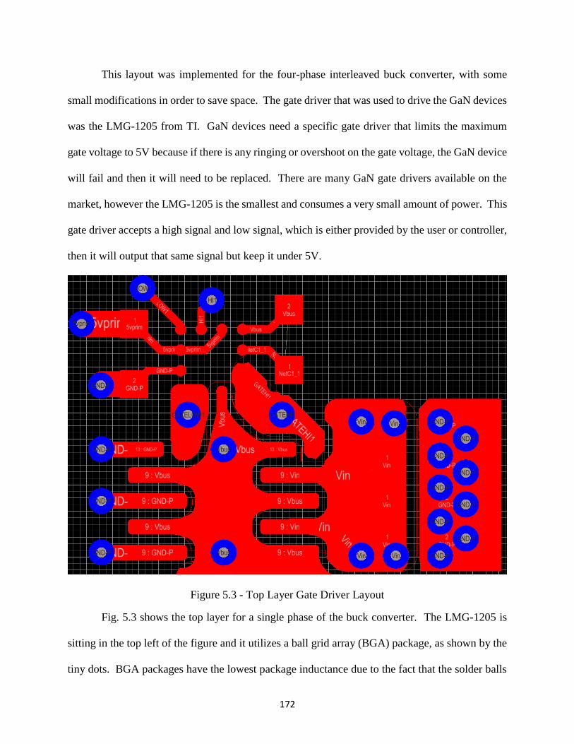
172
This layout was implemented for the four-phase interleaved buck converter, with some
small modifications in order to save space. The gate driver that was used to drive the GaN devices
was the LMG-1205 from TI. GaN devices need a specific gate driver that limits the maximum
gate voltage to 5V because if there is any ringing or overshoot on the gate voltage, the GaN device
will fail and then it will need to be replaced. There are many GaN gate drivers available on the
market, however the LMG-1205 is the smallest and consumes a very small amount of power. This
gate driver accepts a high signal and low signal, which is either provided by the user or controller,
then it will output that same signal but keep it under 5V.
Figure 5.3 - Top Layer Gate Driver Layout
Fig. 5.3 shows the top layer for a single phase of the buck converter. The LMG-1205 is
sitting in the top left of the figure and it utilizes a ball grid array (BGA) package, as shown by the
tiny dots. BGA packages have the lowest package inductance due to the fact that the solder balls

173
are directly connected to the die where the IC lies. The EPC2045 also used a BGA package, which
helps with improving the losses of the devices. The only drawback to a BGA package is that once
the device is placed on the board, it cannot be removed without replacing the device entirely. A
designer may pay the price of wasting devices if they are not soldered on properly. However, the
gate driver layout shown follows Fig. 5.2 closely in order to minimize the gate loop inductance.
Figure 5.3 - 3D Rendering of Gate Driver Layout
Fig. 5.3 shows the same layout as Fig. 5.2, however now it is rendered in 3D. Some things
to note about this layout is that there are no gate resistors. When using the development board
from chapter 2, there were no issues driving each EPC at 500 kHz, so no gate resistors were added.
This also helps with the size of the board because adding gate resistors would increase the size of
the board by a couple of millimeters, which would hurt the overall power density. However, it is

174
recommended for most applications that gate resistors are used, but since this was able to be tested
it is fine not to use them here. The capacitor in the top left of the figure is the decoupling capacitor
for input voltage to the gate driver. The capacitor on the right side of the gate driver is the bootstrap
capacitor, which is needed to drive the top side GaN device. The bootstrap can be connected to
the right of the device because there are two separate locations on the driver that connect to the
switching node, so it save space overall. Finally, the input capacitors are located in the bottom
right. The capacitors are very small in order to save space between each phase of the buck
converter. On the bottom of the board, there are large input capacitors that actually provide the
capacitance for the board. The input capacitors on the top are just there to minimize the loop
inductance. Without those capacitors, the power loop would be vertical and consequently have
the largest parasitic inductance. It does not matter what value the capacitors are on the top of the
board, just as long that there is capacitance there, the loop will be minimized.
Figure 5.4 - Four-Phase Gate Layout
Fig. 5.4 shows the full gate driver layout for the four-phase interleaved buck converter. In
order to keep each phase as symmetric as possible, the gate driver layout for one phase is the same
as all the others. Keeping the layout the same for each phase is important because it minimizes
the difference in path resistance for each phase. If the path resistance is very different between
phases, then it is possible that phase will the lowest resistance will carry more current than the
others will and cause unbalance between each phase. The goal when laying out the buck converter
is to keep each phase as close to one another as possible.

175
5.3 Inductor Layout
The next part in the buck converter layout is to make the windings for the inductor. In
chapter 3, the magnetics were optimized and a design was chosen. This section will discuss how
to implement the design from chapter 3 into a PCB. The windings cannot be connected in any
way that the designer wishes, they will need to be connected in a certain way so that the current
will be shared evenly through each set of windings. ANSYS Maxwell will be used measure the
current in each winding to ensure that current is evenly distributed between them. Lastly, the PCB
implementation of the coupled inductors will be shown.
Recalling chapter 3, the chosen magnetics design was two separate coupled inductors with
six-turns each. The most important part of coupled inductor for the layout is the number of turns
and the number of layers. From chapter 1, it decided that a 14 layer PCB would be used with 12
of those layer being available for the windings. With 12 layers and 6 turns, there will be two
paralleled windings paths. There will be six windings or layers connect in series with another six
windings connected in parallel. The goal will be to use ANSYS Maxwell to look at current sharing
between each set of paralleled windings.

176
Figure 5.5 - Cross Sectional View of Coupled Inductor
Fig. 5.5 shows the cross sectional view of the coupled inductor with each of the windings
labeled. The winding number corresponds with the layer number on the PCB. In Maxwell, each
of the windings will be connected via their external circuit editor program and it will be simulated
at full load with the expected current at that operating point. This will be done in 2D because as
it was explained earlier, the computers in the lab do not have enough power to run 3D transient
analysis.
Figure 5.6 - Winding Connection for Coupled Inductor

177
Fig. 5.6 shows one way that the windings can be connect on the actual PCB. The winding
number corresponds to the layer number in Fig. 5.5. For example, winding one and winding two
are connected in parallel and then this is repeated six times. This is equivalent to six turns because
if two single windings are connected in parallel, they equal a single turn, which when added
together will all the others equals six turns. Note that this is not the only way to connect the
windings together, this is just one example, there are millions of ways to connect them tougher.
Fig. 5.6 can be directly input into Maxwell with a current source, which is the expected current
that should pass through the inductor, and the current in each winding can be measured.
Figure 5.7 - Current Distribution in the Inductor Windings
Fig. 5.7 shows the current distribution output from Maxwell. The red curve represents the
source current provided by the user and the blue and purple waveforms are the output current
coming out of windings 11 and 12. From this plot, the current are wildly unbalanced with the
current even flowing in the opposite direction. When each winding is paralleled with each other,
there is a possibility that current will circulate between each winding in parallel. This is not good
because it will increase the winding loss for the inductor and cause certain windings to heat up
more than others. The inductor was designed with the assumption that the current was balanced

178
in each winding, so the loss calculation is based on perfect balancing. If there is any unbalance, it
means that the original model for windings loss will underestimate the total loss. By looking at
this plot, having paralleled windings allows current to circulate, which is undesirable, so a different
construction is necessary.
Figure 5.8 - New Winding Connection for Coupled Inductor
Fig. 5.8 shows the new winding configuration for the coupled inductor. In this connection,
there are six turns in series and then those six turns are paralleled with each other. This effectively
still gives six turns to the inductor, but ideally, it will halve the current so that it splits evenly
between each path. There is less likely of a chance for circulating current because all of the current
would need to flow through one path and back the other to the input. The resistance is too large
on each path for current to circulate.

179
Figure 5.9 - Current Distribution for New Winding Structure
Fig. 5.9 shows current distribution for the new winding structure. Once again, the current
in windings 11 and 12 are being measured because they are at the output of the inductor windings.
Since each windings is in series with each other, they should all have the same current flowing
through them. It does not matter which pair is measured, as long as they are on opposite windings
paths. In this case, the current is fairly balanced with only small discrepancies between windings
11 and 12. This was the best combination of windings that was found, so this is the final windings
structure that will be used in the PCB layout.
Now that the proper winding arrangement is known, the windings can be constructed in
Altium PCB software. Since the core is ordered separately from the PCB, the only part of the
inductor that needs to be constructed is the windings. From this design, there will be six turns in
series with another six in parallel, which will be followed by a sensing resistor and the output
capacitors. Since the LM-5170 is being used, there needs to be a sensing resistor for each phase
current, which will be connected at the end of the inductor when the windings complete. Directly
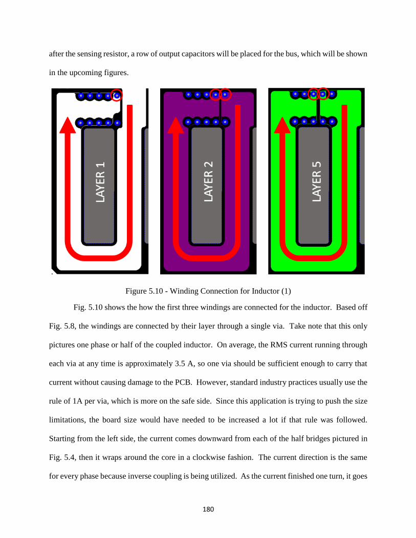
180
after the sensing resistor, a row of output capacitors will be placed for the bus, which will be shown
in the upcoming figures.
Figure 5.10 - Winding Connection for Inductor (1)
Fig. 5.10 shows the how the first three windings are connected for the inductor. Based off
Fig. 5.8, the windings are connected by their layer through a single via. Take note that this only
pictures one phase or half of the coupled inductor. On average, the RMS current running through
each via at any time is approximately 3.5 A, so one via should be sufficient enough to carry that
current without causing damage to the PCB. However, standard industry practices usually use the
rule of 1A per via, which is more on the safe side. Since this application is trying to push the size
limitations, the board size would have needed to be increased a lot if that rule was followed.
Starting from the left side, the current comes downward from each of the half bridges pictured in
Fig. 5.4, then it wraps around the core in a clockwise fashion. The current direction is the same
for every phase because inverse coupling is being utilized. As the current finished one turn, it goes
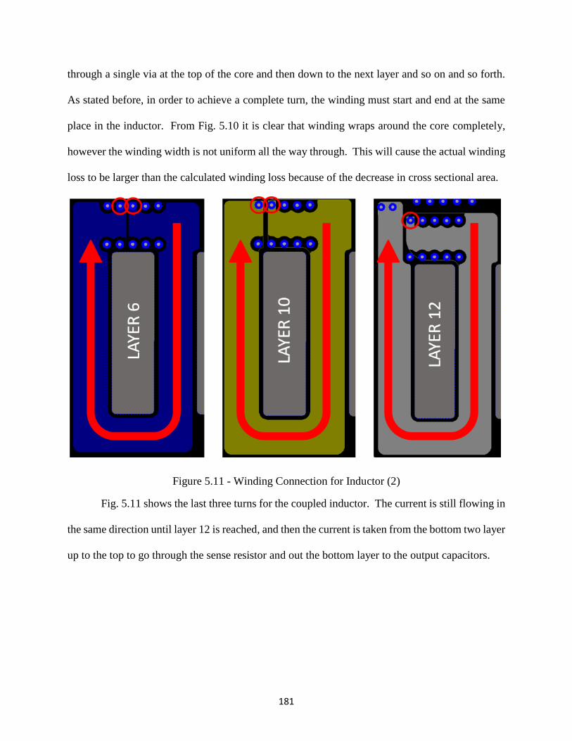
181
through a single via at the top of the core and then down to the next layer and so on and so forth.
As stated before, in order to achieve a complete turn, the winding must start and end at the same
place in the inductor. From Fig. 5.10 it is clear that winding wraps around the core completely,
however the winding width is not uniform all the way through. This will cause the actual winding
loss to be larger than the calculated winding loss because of the decrease in cross sectional area.
Figure 5.11 - Winding Connection for Inductor (2)
Fig. 5.11 shows the last three turns for the coupled inductor. The current is still flowing in
the same direction until layer 12 is reached, and then the current is taken from the bottom two layer
up to the top to go through the sense resistor and out the bottom layer to the output capacitors.

182
Figure 5.12 - Top View of Buck Converter Layout
Fig. 5.12 shows a 3D rendering of the buck converter. As shown in the last figure, the
output from the inductor will go to the top layer through a sense resistor and then to the output
capacitors. There are four sensing resistors, one for each phase, so the current can be monitored
in each phase. It may look like that there are only six bus capacitors on the top layer, but there is
a row of 25 more bus capacitors on the bottom side of the board, which will be shown later in the
final construction. Using the estimated layout for the entire two-stage converter, the power will
flow out to the left side and downward to the LLC.
5.4 Cooling System

183
The previous sections discussed the layout for the buck converter and how the inductor
was constructed in the PCB. The focus of this thesis will now shift toward experimental setup and
results. This section briefly covers the cooling system used for the buck converter, which is also
the cooling system for the entire two-stage converter, but this section will only talk about the buck
converter.
In section 2.4, the electro-thermal design was discussed and it was used to estimate the
temperature of the devices when they would be a full power. The issue with this section is that it
was only conducted at one single inductance value. If the designed inductor from chapter 3 would
be the same as the inductor used in chapter 2, then the analysis would be valid and should match.
However, the inductor used in chapter 2 had an inductance of 7 μH, while the equivalent steady
state inductance of the inductor in chapter 3 is 2.8 μH. The ripple will be twice as large for the
designed inductor, which means a higher peak and lower valley current. With a higher peak and
lower valley current the turn on loss will decrease but the turn off will increase. In addition to
different switching losses, the RMS current will be slightly higher, so the conduction loss will be
higher. It is expected that buck converter devices will heat up more than the temperature measured
in chapter 2.4.
The simplest way to cool a power converter without designing a cold plate or any type of
heat sink that would fit on a device with an area of 4 mm2, is to just use a fan. An NMB axial fan
was used to blow air across the buck converter and cool the devices so that they would not become
too hot. The flow rate of the fan is 0.0519 m3/s (110 ft3/min), which is a fairly slow flow rate, but
it is able to keep the devices from operating at an unsafe temperature.

184
Figure 5.13 - Direction of Air Flow on Buck Converter
Fig. 5.13 shows the direction of the airflow on the constructed buck converter. The fan is
placed at the bottom side of the board and air is blown toward the input of the buck converter.
There is plenty of space for air to flow because there is nothing blocking the board, the pin headers
for measurements are located on the outside of the board and do not interfere with the airflow.
5.5 Functional Open Loop Testing
In this section, the open loop setup and measurements for the inductor will be shown. Since
this is a buck converter, the operation is simple, so not much equipment is needed for open loop
testing. The experimental results will be shown in the following chapter, while this chapter will
discuss the setup.
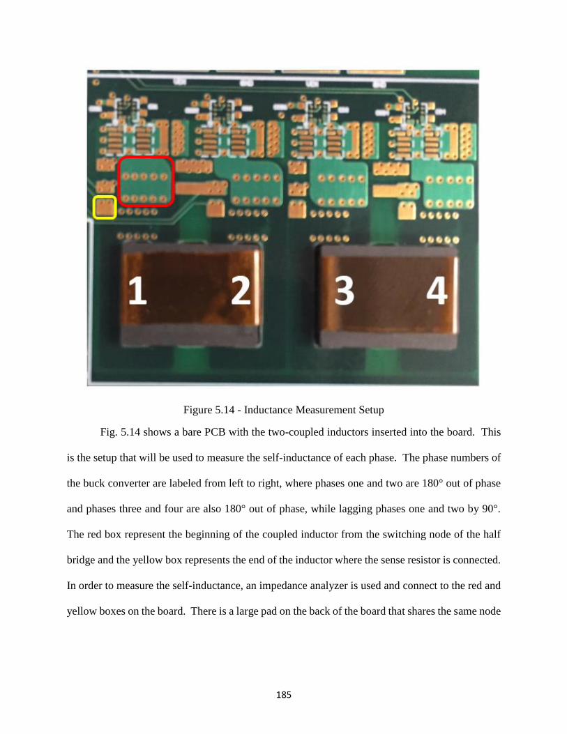
185
Figure 5.14 - Inductance Measurement Setup
Fig. 5.14 shows a bare PCB with the two-coupled inductors inserted into the board. This
is the setup that will be used to measure the self-inductance of each phase. The phase numbers of
the buck converter are labeled from left to right, where phases one and two are 180° out of phase
and phases three and four are also 180° out of phase, while lagging phases one and two by 90°.
The red box represent the beginning of the coupled inductor from the switching node of the half
bridge and the yellow box represents the end of the inductor where the sense resistor is connected.
In order to measure the self-inductance, an impedance analyzer is used and connect to the red and
yellow boxes on the board. There is a large pad on the back of the board that shares the same node

186
as the red box, which makes it easier to connect a wire on the board. An Agilent 4294A precision
impedance analyzer was used to measure the inductance and the results are shown in Table 5.1.
Table 5.1 - Measured Inductance Values
Phase Number Measured Inductance Value
Phase 1 3.526 μH
Phase 2 3.488 μH
Phase 3 3.513 μH
Phase 4 3.620 μH
The measured inductance values are fairly close to one another, with the designed value
set at 3.5 μH. The reason why the inductances are slightly different is because of the air gap placed
on the I-bar. Kapton tape is used to gap the cores because of availability and its high operating
temperature (up to 400 °C). The core is expected to heat up to approximately 90 °C, so the tape
that is used for the air gap needs to be able to survive the high temperature. However, the Kapton
tape is place on by hand, so it is very difficult to get the same thickness across the entire core.
There are bound to be some discrepancies, but as long as all of the air bubbles in the Kapton tape
are removed, the measured inductances should be close to one another. The slight differences in
inductance should not affect the overall operation of the buck converter either because the values
are close together.
The next step for the open loop testing is to setup the gate signals for each phase. The most
important part of the gate signals when driving GaN is the dead time between the top and bottom
switch signals. Dead time is used to separate the high side and low side signal in a half bridge
configuration to ensure that there is not a short circuit during operation. For most circuits with
regular silicon MOSFETs, the dead time is anywhere from 15 ns to 40 ns, however for GaN devices
it is slightly different. Unlike silicon devices, GaN devices do not have a diode in parallel with
the switch, which leads to no reverse recovery loss, but the GaN device can reverse conduct.

187
Reverse conduction occurs when current flows back through the channel from source to drain. In
a GaN device if any amount of current flows back through the channel in the opposite direction,
the temperature of the device will rise rapidly. With a DC current of only two amps, the device
can heat up to over 70 °C, which is very hot for only a few amps of current. This phenomenon
only occurs during dead time operation, so in order to minimize this, the dead time needs to be as
close to zero seconds as possible, without allowing a short circuit to occur. In order to do this, the
gate signals will need to be measured to show that the gates transition near the threshold voltage
of the devices.
Figure 5.15 - Dead Time Generation Circuit
Fig. 5.15 shows the circuit that will be used to generate the dead time for each phase of the
buck converter [30]. The dead time circuit only takes one input, which is the high side PWM
signal for each phase, and then it outputs complementary signals for both high and low side
switches for each phase. In this circuit, the turn on speed is controlled because the diode blocks

188
the voltage when the signal is applied, and then when current flows back through the circuit, it
goes through the diode with close to zero impedance. A designer can control the turn off speed of
a signal if the diode is flipped around. The dead time is controlled by each of the resistors, where
if the value is increased the dead time becomes larger and if the value is decreased, the dead time
becomes smaller. The two capacitors are high frequency decoupling capacitors for filtering out
common mode noise, which have values of 100 pF each.
There is no set equation that defines what resistor value is needed to get the appropriate
amount of dead time. The designer will have to start with a resistor and measure the dead time for
each phase in order to achieve the optimal separation. The typical value for the dead time resistors
is around 100 Ω, but that can vary a lot depending on layout. One single case will be shown for
the optimal dead time separation and then the values for each phase will be shown to what gave
the optimal dead time.

189
Figure 5.16 - High Side Gate Signal
Fig. 5.16 shows the high side gate signal turn on for a single phase on the buck converter.
The blue waveform is the high side gate signal and the yellow waveform is the low side gate signal
coming from the LMG-1205. In this case, the dead time was optimized to have the gate signal
cross each other when they each are at 800 mV. The EPC2045 datasheet states that the minimum
threshold voltage is 800 mV, so this dead time is optimized perfectly because it crosses right at the
threshold and does not leave any time for reverse conduction. Since the dead time circuit is
controlling turn on, the blue waveform is not sharp, but rather has a gradual increase until it reaches
its final level.
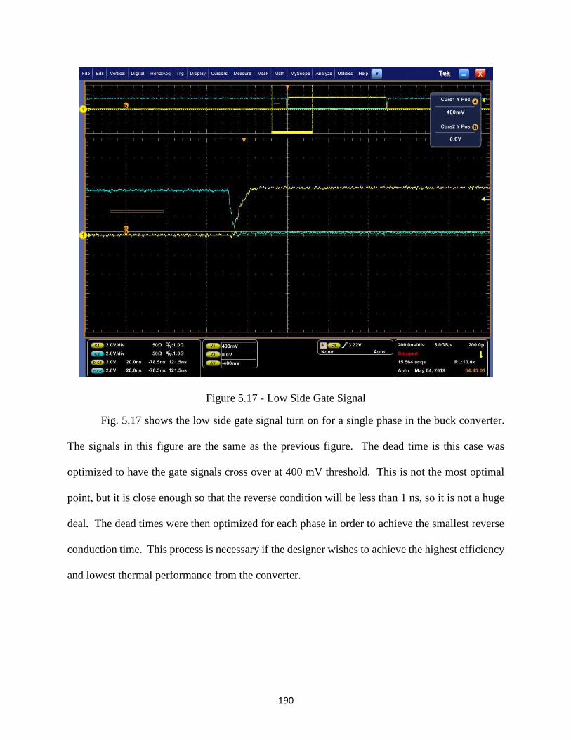
190
Figure 5.17 - Low Side Gate Signal
Fig. 5.17 shows the low side gate signal turn on for a single phase in the buck converter.
The signals in this figure are the same as the previous figure. The dead time is this case was
optimized to have the gate signals cross over at 400 mV threshold. This is not the most optimal
point, but it is close enough so that the reverse condition will be less than 1 ns, so it is not a huge
deal. The dead times were then optimized for each phase in order to achieve the smallest reverse
conduction time. This process is necessary if the designer wishes to achieve the highest efficiency
and lowest thermal performance from the converter.

191
Table 5.2 - Dead Time Resistor Values
RDTHIGH RDTLOW
Phase 1 39 Ω 510 Ω
Phase 2 39 Ω 510 Ω
Phase 3 39 Ω 510 Ω
Phase 4 39 Ω 510 Ω
Table 5.2 shows the dead time resistor values for both the high and low side gate signals.
In this case, all of the high and low dead time resistors were the same value within the resistor
tolerance. This is not always true, one would need to measure each phase gate signals in order to
verify the correct dead time, which was done in this case.
With every part now accounted for, the open loop testing can now begin. The open loop
hardware and equipment will be shown and then the experimental results for the open loop will be
discussed in the next chapter.

192
Figure 5.18 - Equipment for Open Loop Testing
Fig. 5.18 shows the equipment that was used for the open loop testing. Since this is a four-
phase interleaved buck converter, two separate Tektronix AFG3102 were used to supply the gate
signals for the converter. The converter will operate at 48V to 36V/28A, so two RBL electronic
loads were needed because they only can supply 800W each. A 1500W TDK-Lambda power
supply was used to supply the input voltage and an Agilent E3631A was used to supply the gate
drivers. Since this is open loop, none of the auxiliary circuits were used, everything was supplied
externally and the loss was calculated from the front panel display. As discussed earlier, a NMB

193
fan was used to cool the devices operating at 0.0519 m3/s (110 ft3/min). Finally, a Tektronix
MSO5104B oscilloscope was used to measure all of the waveforms from the buck converter.
Figure 5.19 - Open Loop Setup for Buck Converter
Fig. 5.19 shows the connections to the prototype board from the open loop setup pictured
in the previous figure. This figure just shows the buck converter assembled on the prototype board
as this section only discusses the buck results. The gate signals come from the Tektronix
AFG3102, which are shown on the left side of the board. The gate drivers are powered from the
Agilent power supply which comes from the top left of the board. The dead time circuit is
underneath the controller board, so open loop and closed loop can easily be switched between.
The input comes from the top of the board which is provided by the TDK-Lambda power supply
and the output of the buck flows out to the left side of the board where it goes to the RBL electronic
loads. Extra input capacitance was necessary when the controller was added because the input

194
source was not good enough to regulate 48V on the input over all load conditions. The red square
shows the four-phase interleaved buck converter with the input and output capacitance on the
backside of the board. Finally, both passive and differential probes were used to measure the
signals from the buck. Passive probes were used to measure the switching node voltages because
in this lab on 42V differential probes were available. The differential probes were used to measure
the low side gate signals for each phase and the output voltage. Once again, the high side gate
signals need passive probes because the differential probes cannot measure that high of voltage.
Not pictured here, a TCP030A was used to measure the phase currents during nominal operation.
In order to measure the current, a long wire had to be added where the sense resistor is placed, so
that the current probe could fit and clamp around the wire. All probes used have 1GHz of
bandwidth.
Chapter 6. Experimental Evaluations
6.1 Buck Converter Results
In this chapter, the converter results will be shown and discussed. The open loop results
for the buck converter will be shown, in addition to the buck, the open loop efficiency will be
shown for the two-stage converter. To close the results section, the closed loop results with the
LM-5170 will be shown with the buck converter. It is also important to note that two different
board iterations were used when testing the converter. The open loop testing was done on the first
iteration of the two-stage converter and the closed loop testing was done on a different board,
which was the second iteration of the board.
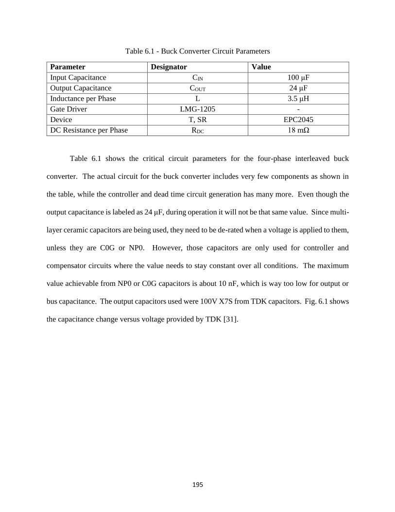
195
Table 6.1 - Buck Converter Circuit Parameters
Parameter Designator Value
Input Capacitance CIN 100 μF
Output Capacitance COUT 24 μF
Inductance per Phase L 3.5 μH
Gate Driver LMG-1205 -
Device T, SR EPC2045
DC Resistance per Phase RDC 18 mΩ
Table 6.1 shows the critical circuit parameters for the four-phase interleaved buck
converter. The actual circuit for the buck converter includes very few components as shown in
the table, while the controller and dead time circuit generation has many more. Even though the
output capacitance is labeled as 24 μF, during operation it will not be that same value. Since multi-
layer ceramic capacitors are being used, they need to be de-rated when a voltage is applied to them,
unless they are C0G or NP0. However, those capacitors are only used for controller and
compensator circuits where the value needs to stay constant over all conditions. The maximum
value achievable from NP0 or C0G capacitors is about 10 nF, which is way too low for output or
bus capacitance. The output capacitors used were 100V X7S from TDK capacitors. Fig. 6.1 shows
the capacitance change versus voltage provided by TDK [31].
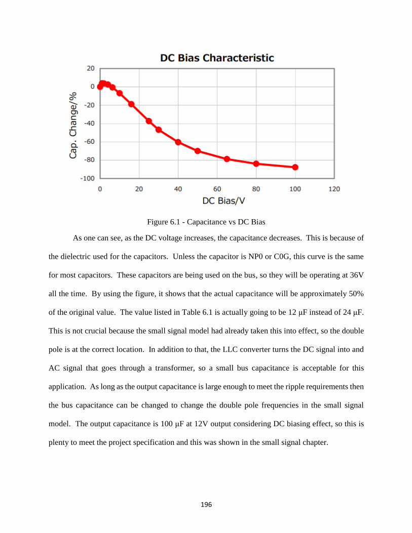
196
Figure 6.1 - Capacitance vs DC Bias
As one can see, as the DC voltage increases, the capacitance decreases. This is because of
the dielectric used for the capacitors. Unless the capacitor is NP0 or C0G, this curve is the same
for most capacitors. These capacitors are being used on the bus, so they will be operating at 36V
all the time. By using the figure, it shows that the actual capacitance will be approximately 50%
of the original value. The value listed in Table 6.1 is actually going to be 12 μF instead of 24 μF.
This is not crucial because the small signal model had already taken this into effect, so the double
pole is at the correct location. In addition to that, the LLC converter turns the DC signal into and
AC signal that goes through a transformer, so a small bus capacitance is acceptable for this
application. As long as the output capacitance is large enough to meet the ripple requirements then
the bus capacitance can be changed to change the double pole frequencies in the small signal
model. The output capacitance is 100 μF at 12V output considering DC biasing effect, so this is
plenty to meet the project specification and this was shown in the small signal chapter.

197
Figure 6.2 - Low Side Gate Signals (1)
Fig. 6.2 shows the low side gate signals for each phase. These gate signals are measured
directly on the output of the gate driver and input to the device. It is important to note that phases
one and two (yellow and blue waveforms) are 180° out of phase and phase three and four (pink
and green waveforms) are also 180° out of phase while lagging the first two phases by 90°. The
phases are shifted this way in order to get the cancelation in the inductors from the inverse
coupling.

198
Figure 6.3 - Low Side Gate Signals (2)
Fig. 6.3 shows the same waveforms as the previous figure, however it is now zoomed in
and the signals are interleaved. In this figure, it shows that the phase shifting between each phase
is almost exactly the same. The slight gap between each signal is from the dead time, which
ensures that none of the synchronous rectifiers is on at the same time. If two or more of the
synchronous rectifiers were on in this application, there would be circulating current through
separate two or more phases, which means that power is not being delivered to the load, which in
turn will increase losses. Another concern from this scope capture is the noise that is apparent on
the low side phase one gate signal. This is measurement noise and not the actual gate signal. The
issue with designing a very small board, the measurement signals have to cross the power planes,
so each phase will show up on every waveform, which will be shown in the upcoming figures.

199
The equivalent switching frequency of the buck is 2 MHz, so every 500 ns, noise will show from
every phase. This is not a terrible issue; one just has to remember that it is only measurement
noise. If it were the actual signal, then there would be short on every phase during each cycle,
which would cause the converter to fail and devices to explode. As the converter load increases,
the noise will become more apparent on each phase.
Figure 6.4 - Inductor Current for Phases One and Two
Fig. 6.4 shows the inductor currents for phases one and two. The green and yellow
waveforms are the phase one and phase two inductor currents, respectively. At full load it is clear
that both average currents are the same at approximately 6.9 A. The peak and valley of the currents
are 10.4A and 3.5A respectively. This is fairly close to the calculation value of 3.5 μH, however
the current peak and valley is a little larger. This current waveform represent a phase inductance
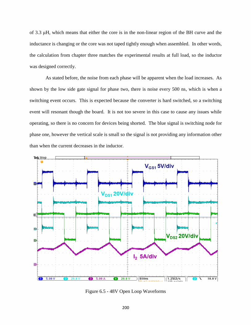
200
of 3.3 μH, which means that either the core is in the non-linear region of the BH curve and the
inductance is changing or the core was not taped tightly enough when assembled. In other words,
the calculation from chapter three matches the experimental results at full load, so the inductor
was designed correctly.
As stated before, the noise from each phase will be apparent when the load increases. As
shown by the low side gate signal for phase two, there is noise every 500 ns, which is when a
switching event occurs. This is expected because the converter is hard switched, so a switching
event will resonant though the board. It is not too severe in this case to cause any issues while
operating, so there is no concern for devices being shorted. The blue signal is switching node for
phase one, however the vertical scale is small so the signal is not providing any information other
than when the current decreases in the inductor.
Figure 6.5 - 48V Open Loop Waveforms
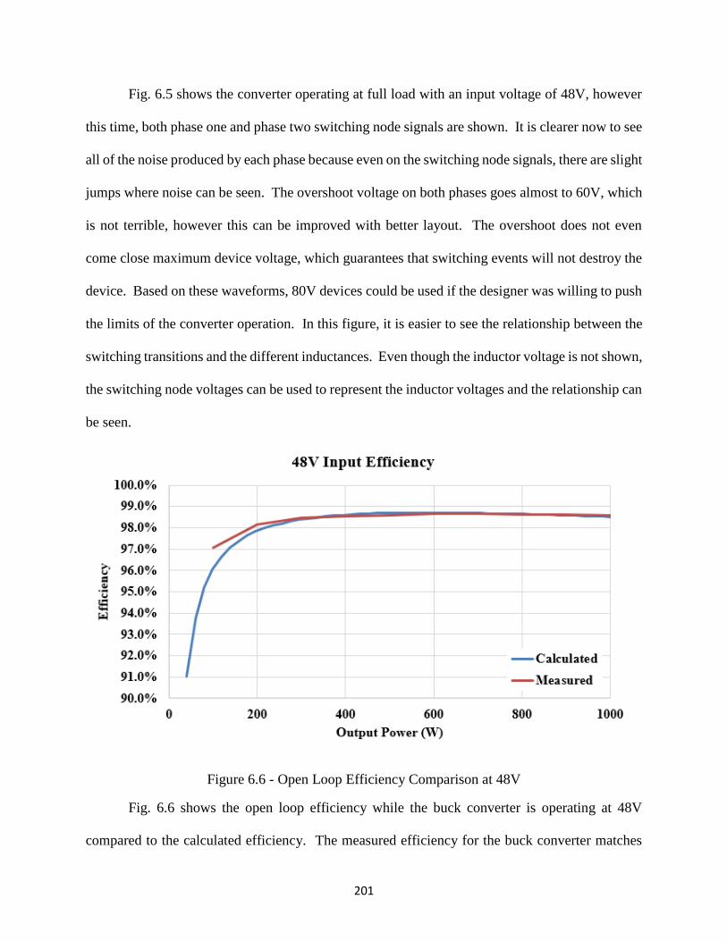
201
Fig. 6.5 shows the converter operating at full load with an input voltage of 48V, however
this time, both phase one and phase two switching node signals are shown. It is clearer now to see
all of the noise produced by each phase because even on the switching node signals, there are slight
jumps where noise can be seen. The overshoot voltage on both phases goes almost to 60V, which
is not terrible, however this can be improved with better layout. The overshoot does not even
come close maximum device voltage, which guarantees that switching events will not destroy the
device. Based on these waveforms, 80V devices could be used if the designer was willing to push
the limits of the converter operation. In this figure, it is easier to see the relationship between the
switching transitions and the different inductances. Even though the inductor voltage is not shown,
the switching node voltages can be used to represent the inductor voltages and the relationship can
be seen.
Figure 6.6 - Open Loop Efficiency Comparison at 48V
Fig. 6.6 shows the open loop efficiency while the buck converter is operating at 48V
compared to the calculated efficiency. The measured efficiency for the buck converter matches

202
fairly well across all load ranges. The major discrepancy is that at full load the calculation has a
lower efficiency than the measured. At this point, the core loss is dominating the loss breakdown,
so there might be some discrepancy between the actual and calculated core loss. In the calculation,
it is assumed that the core is at the optimal temperature, but in measurement, the core temperature
increases with the load, so the temperature will change the core loss slightly. The calculated
response peaks at 400W, which is right around critical operation, where the measure response
peaks around 700W, which is just above the critical operation point in the converter. Since the
inductance is slightly lower than the designed value when operating, it makes sense that the peak
is there because the top switch is turning on in ZVS.
Figure 6.7 - 60V Open Loop Waveforms
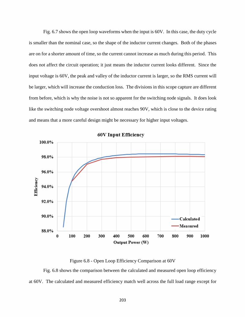
203
Fig. 6.7 shows the open loop waveforms when the input is 60V. In this case, the duty cycle
is smaller than the nominal case, so the shape of the inductor current changes. Both of the phases
are on for a shorter amount of time, so the current cannot increase as much during this period. This
does not affect the circuit operation; it just means the inductor current looks different. Since the
input voltage is 60V, the peak and valley of the inductor current is larger, so the RMS current will
be larger, which will increase the conduction loss. The divisions in this scope capture are different
from before, which is why the noise is not so apparent for the switching node signals. It does look
like the switching node voltage overshoot almost reaches 90V, which is close to the device rating
and means that a more careful design might be necessary for higher input voltages.
Figure 6.8 - Open Loop Efficiency Comparison at 60V
Fig. 6.8 shows the comparison between the calculated and measured open loop efficiency
at 60V. The calculated and measured efficiency match well across the full load range except for

204
the slight difference at full load. The measured efficiency reaches slightly above 98% at
approximately 800W, which is a different peaking than the 48V case. The current ripple is larger,
so the converter goes into critical mode at a higher power, so the optimal point is at a higher power.
With a larger current ripple, the di/dt in the core is larger, so there is a larger core loss, which is
the main contributing factor to the drop in efficiency.
Figure 6.9 - 40V Open Loop Waveforms
Fig. 6.9 shows the open loop waveforms when the input is at 40V. In this case, the duty
cycle is larger than the previous two cases, which leads to a different current waveform. This
overshoot on the switching node waveforms only reach 50V, which is expected and the noise is
not as major on the other waveforms. With the input voltage being 40V, the inductor current ripple
is smaller, meaning that the RMS current will decrease, decreasing the conduction loss. In addition

205
to decreasing conduction loss, the di/dt is smaller in the core, so the core loss should also decrease,
leading to higher efficiency.
Figure 6.10 - Open Loop Efficiency Comparison at 40V
Fig. 6.10 shows the comparison between the calculated and measured open loop efficiency
at 40V input. Once again, there is a large discrepancy between the calculated and measured result
at heavy load, which is again attributed to the core loss calculation. The peak value reach 99%
efficiency at approximately 600W, which is a higher efficiency than the nominal case and occurs
at a lower output power. The higher efficiency is expected at a lower input voltage because all of
the losses in the converter are lower than the other cases.

206
Figure 6.11 - Measured Open Loop Efficiency Comparison
Fig. 6.11 shows the measured open loop efficiency comparison at different input voltages.
As expected, the 40V input has the best efficiency and the 60V input has the worst efficiency.
This is due to the fact that the losses in the buck converter are smaller when the input voltage is
closer to the output voltage and they increase as the input voltage deviates from the output voltage.
This can be attributed to the increasing current ripple, which increases conduction loss, switching
loss, and core loss. Intuitively, the most efficient way to transfer electrical power is to directly
connect the source to the load. If a buck converter is directly connected to the load, it means that
the duty cycle would be at 100%. Relating to this statement, the higher the duty cycle, the higher
the efficiency, which is why the 40V input has the highest efficiency with a duty cycle of 0.9. The
results are what was expected with the nominal input voltage reaching a peak efficiency of 98.6%.

207
Figure 6.12 - Thermal Image of Buck at 48V Input
Fig. 6.12 shows a thermal image of the buck converter operating at the nominal input
voltage at 1 kW input. From this image is shows that top switch heats up to 113 °C at full load,
which is higher than what was expected. From chapter two, it was expected to only reach about
100 °C, but here it exceeds that by a little bit, which is not too bad. The highest temperature for
safe operation is 155 °C, which the converter is not close to, so this is fine, the only issue is that
cooling will be needed if this was to be placed in a 55 °C ambient temperature as specified by the
project. The discrepancy between the expected and actual temperature is due to the fact that
inductor that was used for the evaluation board was 7 μH and very large. This means that the core
loss was almost non-existent for the test that was done and the current had a smaller ripple. With
a smaller current ripple, the devices do not heat up as much, which is directly attributed to the
current ripple, which is determined by the inductance. The temperature was hotter for the 60V
case and cooler for the 40V case.

208
The open loop results for the buck converter were presented in this section and they were
able to achieve expected efficiency markers. The high efficiency of the buck converter can be
attributed to the low phase current and high duty cycle. This will be necessary for the overall
efficiency of the two-stage converter because the LLC will be conducting three times the amount
of current as the buck converter. With three times the current, the losses will be larger in the LLC
even though it will be operating with ZVS. The high efficiency of the buck converter will help
the two-stage converter reach project specifications of 95% efficiency.
6.2 Two-Stage Results
The previous section showed the results for the open loop four-phase interleaved buck
converter. This section will be brief and shows the efficiency curve for the two-stage converter at
the nominal input voltage. The LLC design and open loop results will not be discussed in the
section or thesis.

209
Figure 6.13 - Two-Stage Converter
Fig. 6.13 shows the assembled two-stage converter. This picture is similar to the previous
one shown in the last section; however, this was an earlier iteration of the board with a different
controller. This iteration of the board was used for the open loop testing, but not for closed loop
testing as the controller did not work. The LLC converter is about 1.75 times larger than the buck,
which is expected because it handles more current and requires larger magnetics. Not pictured
here, but the back of the board has all of the resonant capacitors, which occupy a large amount of
space because a precise capacitance is required to have the resonant frequency operate a 1 MHz.
The resonant inductance is fixed by the core and air gap, so it is easier to adjust the capacitance,
which requires lots of space.
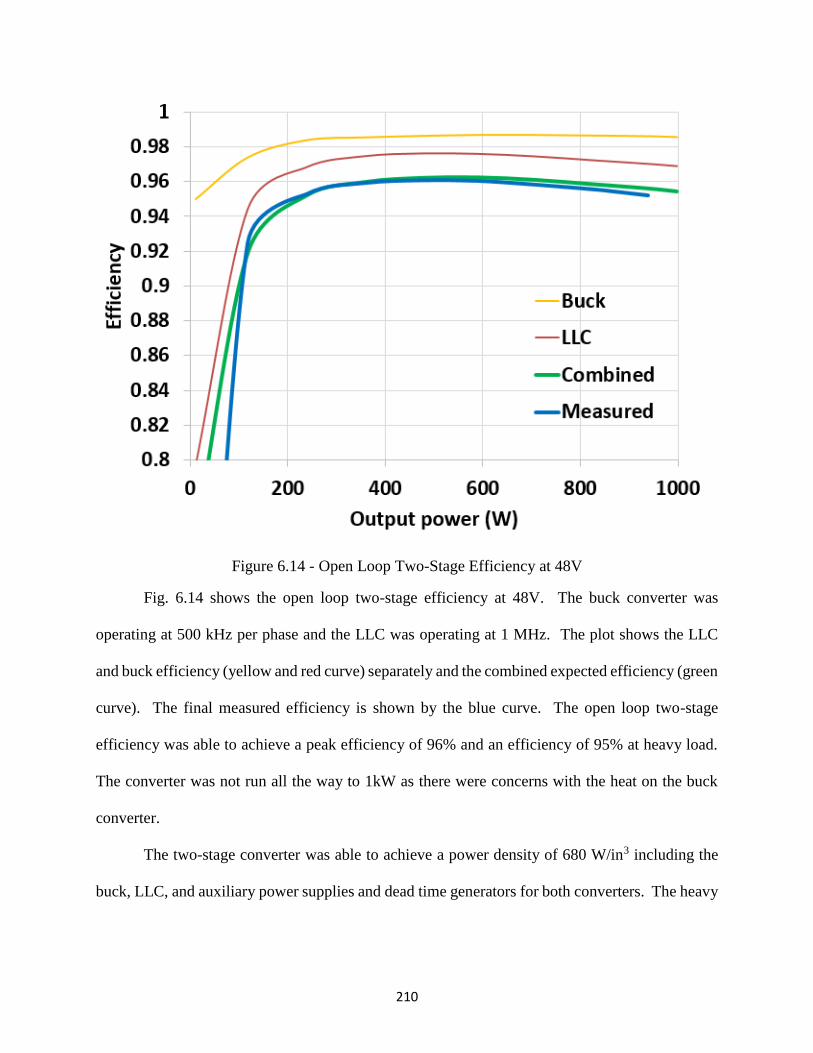
210
Figure 6.14 - Open Loop Two-Stage Efficiency at 48V
Fig. 6.14 shows the open loop two-stage efficiency at 48V. The buck converter was
operating at 500 kHz per phase and the LLC was operating at 1 MHz. The plot shows the LLC
and buck efficiency (yellow and red curve) separately and the combined expected efficiency (green
curve). The final measured efficiency is shown by the blue curve. The open loop two-stage
efficiency was able to achieve a peak efficiency of 96% and an efficiency of 95% at heavy load.
The converter was not run all the way to 1kW as there were concerns with the heat on the buck
converter.
The two-stage converter was able to achieve a power density of 680 W/in3 including the
buck, LLC, and auxiliary power supplies and dead time generators for both converters. The heavy
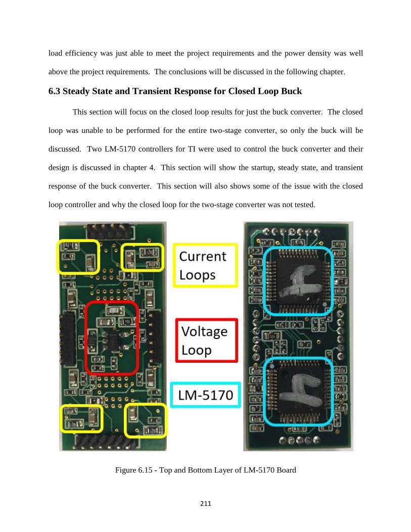
211
load efficiency was just able to meet the project requirements and the power density was well
above the project requirements. The conclusions will be discussed in the following chapter.
6.3 Steady State and Transient Response for Closed Loop Buck
This section will focus on the closed loop results for just the buck converter. The closed
loop was unable to be performed for the entire two-stage converter, so only the buck will be
discussed. Two LM-5170 controllers for TI were used to control the buck converter and their
design is discussed in chapter 4. This section will show the startup, steady state, and transient
response of the buck converter. This section will also shows some of the issue with the closed
loop controller and why the closed loop for the two-stage converter was not tested.
Figure 6.15 - Top and Bottom Layer of LM-5170 Board

212
Fig. 6.15 shows the controller board that houses the two LM-5170 controllers from TI. A
controller board was used in this application because it is easier to assemble on a smaller board,
than on the power board. It the open loop, the dead time needed to be generated by external ICs,
but with the LM-5170, the controller generates dead time internally, so the external circuitry is not
required. However, the board was tested with both open loop and closed loop, so instead of making
a newer generation board with just the controller, a daughter board was made so that testing
between open loop and closed loop could be relatively simple. For a final board version, the dead
time generation used in the open loop would be removed and the two controllers would be put
directly on the power board.
The LM-5170 utilizes average current mode as discussed in chapter four of this thesis.
There are four separate current loops, one for each phase, and one single voltage loop to set the
average current for each phase. With four separate current loops, this allows each phase to be
controlled independently, which allows for each phase to operate independently in case of a failure.
However, it is expected that each phase will be identical to ensure perfect current sharing.

213
Figure 6.16 - Startup Waveform for Buck Converter
Fig. 6.16 shows the startup waveforms for the buck converter at a 48V input. The blue
waveforms are gate signals, the pink waveform is a switching node signal, and the green waveform
is the output voltage of the buck converter. The only signal that matters during the startup is the
output voltage because the gate and switching node signals need a resolution of 800 ns just to be
able to see them. The way the LM-5170 starts the converter is by slowing increasing the duty
cycle on all of the phases until the output voltage is equal to reference signal provided by the
designer. The input slew rate can be chosen by the designer by adding a soft start capacitor to the
controller. In this case the soft start was chosen to be 15 ms, which would slows the output voltage
slew rate down to 3 mV/μs, which would allow for the buck and LLC to start safely without causing
an overcurrent on any device. This is more important for the LLC because when the converter
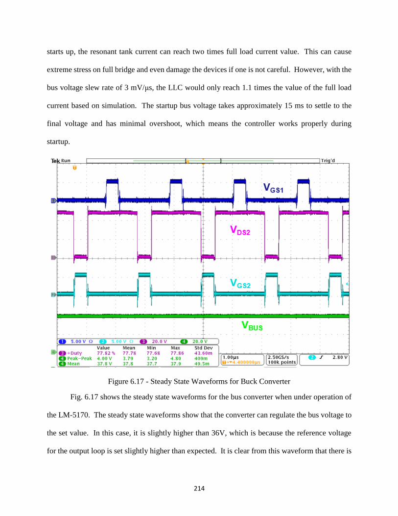
214
starts up, the resonant tank current can reach two times full load current value. This can cause
extreme stress on full bridge and even damage the devices if one is not careful. However, with the
bus voltage slew rate of 3 mV/μs, the LLC would only reach 1.1 times the value of the full load
current based on simulation. The startup bus voltage takes approximately 15 ms to settle to the
final voltage and has minimal overshoot, which means the controller works properly during
startup.
Figure 6.17 - Steady State Waveforms for Buck Converter
Fig. 6.17 shows the steady state waveforms for the bus converter when under operation of
the LM-5170. The steady state waveforms show that the converter can regulate the bus voltage to
the set value. In this case, it is slightly higher than 36V, which is because the reference voltage
for the output loop is set slightly higher than expected. It is clear from this waveform that there is
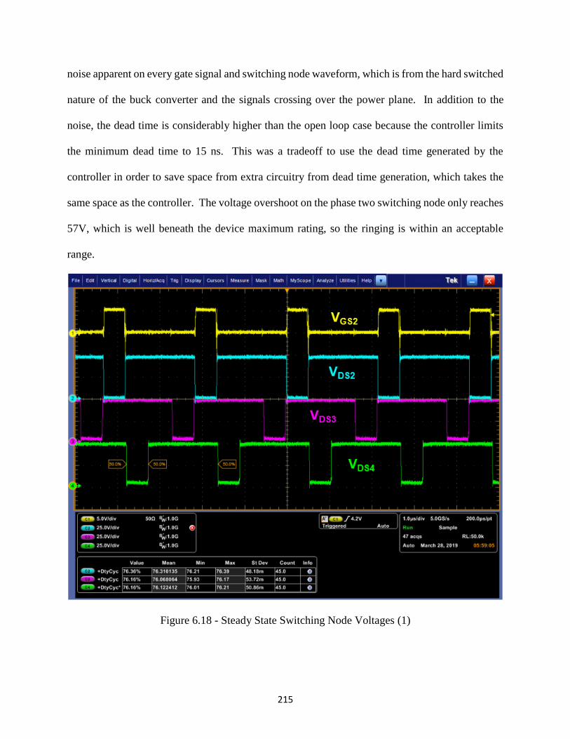
215
noise apparent on every gate signal and switching node waveform, which is from the hard switched
nature of the buck converter and the signals crossing over the power plane. In addition to the
noise, the dead time is considerably higher than the open loop case because the controller limits
the minimum dead time to 15 ns. This was a tradeoff to use the dead time generated by the
controller in order to save space from extra circuitry from dead time generation, which takes the
same space as the controller. The voltage overshoot on the phase two switching node only reaches
57V, which is well beneath the device maximum rating, so the ringing is within an acceptable
range.
Figure 6.18 - Steady State Switching Node Voltages (1)

216
Fig. 6.18 shows the steady state switching node voltages of the buck converter. The
switching node voltages all exhibit the same duty cycle as each other, which means that each phase
is regulating the same output voltage. However, comparing VDS2 to the other switching node
voltages, the rising and falling slopes are not the same. For phase two, the slopes are at sharp 90°
angles, while phases three and four have some slew rate. This is caused by unbalanced current
among the phases with phase two carrying more of the current. In a PWM converter that is hard
switched, the switching node signals exhibit behavior like in phase two, where as in resonant
converters, the device voltage more closes represents phases three and four [32]. This means that
there is not as much current in phases three and four as there is in phase two. With not as much
current in the phases three and four, the remaining current is transfer to phases one and two, which
means higher losses.

217
Figure 6.19 - Steady State Switching Node Voltages (2)
Fig. 6.19 shows the same waveforms as the previous figure, but at a higher power. As
explained previously, the pink and green waveforms were turning on with close to zero current,
meaning phases three and four were operating with ZVS. However, in this figure, the power was
increased to where more current started flowing through each phase of the buck converter. In this
scope waveform, the pink and green waveforms now have sharp transitions, so they are turning on
with some current flowing through the devices, so it is now acting as a hard switched converter
instead of operating at ZVS. By looking at the peaks of each switching node waveform, it is clear
that phase two is slightly larger than phases three and four by a couple of volts. This means that
phase two is conducting more current because the voltage spike is directly related to the parasitic

218
inductance, which is controlled by current. The higher the current, the larger the ringing on turn
on and turn off. Since the peaking is higher on phase two there will more current running through
that phase than the others.
Figure 6.20 - Thermal Image of Closed Loop Buck at 1 kW
Fig. 6.20 shows the thermal image of buck converter operating at 1 kW. In this image, the
phase one and two top devices reach 130 °C, while the phases three and four top devices only are
100 °C. If this is compared to Fig. 6.12, the open loop buck converter, there is a temperature
difference. In the open loop, the temperature of all the devices is approximately 110 °C, where as
in the closed loop the temperature ranges from 100 °C to 130 °C. In the open loop converter, the
dead time was optimized and all of phases had balanced current between them. In the closed loop
converter, dead time is not optimized and the current is unbalanced, which leads to the increase in
temperature on the devices. The current cannot be measured directly in this buck converter
because of the size of the inductors, but by looking at the winding temperature on the board, it can
be seen that there are differences in temperature. Phases one and two have a higher temperature
than phases three and four, so there is more conduction in the first two phases. However, the 30
°C temperature difference between the devices is not a huge deal because the safe operating
temperature for the EPC2045 goes up to 155 °C, so the devices are fine. The devices have been

219
operated at 170 °C temperature before, however when the device temperature increases that high
and operates for a long period of time, the on resistance starts to increase exponentially and the
gate starts to degrade on the devices. It is not recommended to run the devices at high temperatures
for a long period.
The interesting phenomena of Fig. 6.20 is that phases one and two have the same
temperature and phases three and four have the same temperature. This is not a coincidence
because phases one and two are controlled by one controller and phases three and four are
controlled by the second controller. Fig. 6.15 showed the daughter board with two LM-5170’s,
where the chip on the top part of the board controls phases one and two and the chip on the bottom
part of the board controls phases three and four. The controllers are connected by a
synchronization pin that adjusts the clocks so that each phase is shifted to the correct phase angle.
There is a potential issue between the references on both the controllers that is causing current
imbalance.
As explained earlier in chapter four, each LM-5170 gets a control signal from the voltage
loop, ISETA, which is then fed into the transconductance amplifier where the voltage signal is
compared to the current signal. There is one control voltage signal that feeds into two separate
controllers, which then is compared to four separate current loops. The voltage control signal sets
the average current in each phase, so if there discrepancy between the control signals going into
each controller, then there could be current imbalance.

220
Figure 6.21 - ISETA Signals
Fig. 6.21 shows the voltage control signal coming from the outer voltage loop going into
each controller. Each signal was measured directly on the pin of each controller to ensure that the
voltage measured was the one entering the controller. This waveform was taken at 500W output
when the currents were already unbalanced and each control signal is right on top of each other.
There is a 30 mV offset, with the blue waveform being slightly larger than the pink waveform,
which is due to an inherent probe offset. With the offset being ignored, both of the control signals
going into each controller is the same, which means that the average current in each phase should
be the same; however, that is not the case as shown by the thermal waveforms.

221
Another issue that arises by looking at the control voltage waveform is the noise on the
signal. Each phase of the buck converter is operating at 500 kHz, which means that the equivalent
switching frequency at the bus is 2 MHz, so every 500 ns there is a switching event, which is
shown by the previous figure. It was expected that the transconductnace amplifier would filter out
the high frequency noise, but after closer inspection, the transconductance amplifier has a
bandwidth of 4 MHz, so almost everything including white noise will pass through the current
loop. In addition, the differential amplifier that senses the current has a bandwidth 10 MHz, so all
noise passes through that amplifier, which has a gain of x50, which amplifies the noise to what is
being measured in Fig. 6.21. The noise coming from the power board is concerning because it can
cause issues in the analog control loop, which is a possible issue why the currents are imbalanced.
Since the voltage control signal was proven the same for each controller, then the issue
must be with the sensed current signal. It is difficult to prove this because the voltage across the
sense resistor is an average of 30 mV (50 mV max), which is almost next to impossible to measure
accurately, especially since the sense resistor is not in the path to ground, so a differential probe is
needed that can measure that small of voltage. However, it can be shown that current can be
limited by the controller in each phase, so that other phases conduct more current than others.
Using the equations provided by TI in their datasheet for the LM5170, the current in phases one
and two can be limited, while the currents in phases three and four can be unlimited and let to
increase to any value.
In order to limit the current in the converter, each controller has peak current limiting
function that will shut down the controller if that limit is reached. The voltage across the sense
resistor is compared to a peak voltage set by the user and if that peak voltage is exceeded, then the
controller will shut down. In the following scenario, phases one and two are limited to 21 A peak
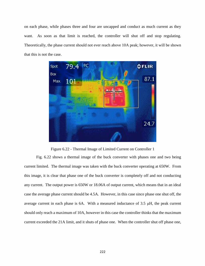
222
on each phase, while phases three and four are uncapped and conduct as much current as they
want. As soon as that limit is reached, the controller will shut off and stop regulating.
Theoretically, the phase current should not ever reach above 10A peak; however, it will be shown
that this is not the case.
Figure 6.22 - Thermal Image of Limited Current on Controller 1
Fig. 6.22 shows a thermal image of the buck converter with phases one and two being
current limited. The thermal image was taken with the buck converter operating at 650W. From
this image, it is clear that phase one of the buck converter is completely off and not conducting
any current. The output power is 650W or 18.06A of output current, which means that in an ideal
case the average phase current should be 4.5A. However, in this case since phase one shut off, the
average current in each phase is 6A. With a measured inductance of 3.5 μH, the peak current
should only reach a maximum of 10A, however in this case the controller thinks that the maximum
current exceeded the 21A limit, and it shuts of phase one. When the controller shut off phase one,

223
the converter actually starts to lose voltage regulation as the output power is increased. Instead of
regulating 36V, the bus voltage will decrease with increasing output current.
The only logical explanation for this phenomenon is that the sense current going into the
controller is not the actually current flowing through the converter. As shown by the open loop,
at full load, the maximum current is only 10.5A, where in the closed loop case; the controller thinks
the phase current is already over 21A. Multiple things including a bad sense resistor and large
parasitic inductances can cause the incorrect current sensing. A non-Kelvin connected sense
resistor was used to measure the current, which can lead to issue when the voltage is measured by
the differential amplifier. A Kelvin connect sense resistor was not used in this application because
the smallest resistor available is twice the size of the current sense resistor. The increase in length
from the sense resistor would drop the overall power density with little benefit. When the sensing
signal is not Kelvin connected, the parasitic inductance (ESL) of the sense resistor becomes a
contributing factor to the sensed current. With an ESL of only 1 nH, the sensed current can give
false peaks and valleys, which will increase the peak of the sensed inductor current. In addition to
the bad sensing, the controller is on a separate board than the buck, so there is extra path resistance
and inductance that is added from the connector to the power board to controller board. On top of
the long connections, the sense resistor is only 3 mΩ, which means the impedance is small to begin
with, so the parasitic inductance will be larger for smaller sense resistor values. The sense resistor
could be increased, but only to 5 mΩ, because that is the limit set by the datasheet for the LM5170
based on the buck converter voltages and currents.
All of the parasitic inductances and path resistance add up and cause issues, which is being
seen by the closed loop in its current state. However, there is a compensation that is added to
adjust for the ESL, but it only works if the value is known. A special type of probe is needed to

224
measure very small inductances for the impedance analyzer, but the lab that the board constructed
in does not have the special probe, so a guess is the best estimate. The only issue with guessing is
that if the guess is wrong, the compensation circuit provides no benefit to the closed loop, it can
actually make it worse. If the compensation capacitor is larger than expected, the sensed current
will have smaller ripple, which would lead to the peak current being wrong and not triggering the
current limit. If the compensation capacitor is smaller than expected, the sensed current will have
a larger and more distorted ripple giving false zero crossings, which is currently happening in the
current state of the buck converter. Fig. 6.23 shows the compensation circuit and equation used to
calculated the compensation capacitor.
Figure 6.23 - Compensation Circuit for ESL of Sense Resistor
In order to compensate the ESL, LCS, the RC time constant for the compensator has to be
equal to the L/R time constant in the power circuit. If the resistors are both the same in the sensing

225
path, then with a known ESL and sense resistor, the compensation capacitor can be calculated. In
the case for the buck converter, the compensation capacitor may be too small, but there is no way
to verify without measuring the signal. Another issue is that the voltage potential at the differential
amplifier is 36V, so a large capacitor is needed (size wise) in order to compensate the ESL. The
two 100 pF capacitors are used to filter out common mode noise on each differential amplifier;
their poles are at very high frequency, so they do not affect the closed loop in a negative way.
The final test in closed loop control is to step the load and see how the output voltage
responds. Due to the issues with the controller not being able to sense the current accurately for
each phase, the load was only stepped from 250W to 500W in order to ensure that the converter
would not become unstable at high load conditions. A load step up and load step down was
performed with a current slew rate of 1 A/μs as specified by the project requirements. It is expected
that the transient response of the buck converter will have higher overshoots and undershoots based
on the output voltage.

226
Figure 6.24 - Load Step Up Buck Converter (500W → 1000W)
Fig. 6.24 shows the load step up for the buck converter. The green waveform is the output
voltage and the pink waveform is the output current divided by four. The output current is
quartered because there are multiple cables connecting the converter to the electronic load. The
load step response is worse than expected from simulation. In simulation it was only expected for
the undershoot to be at 3V, but in experimentation it is 6.4V. This is due to the design of the closed
loop compensators. The overshoot/undershoot is affected by the phase margin and bandwidth of
the closed loop system. From chapter four, the closed loop bandwidth was designed to be 2 kHz
and the phase margin was designed to 64°, for the buck converter only. After matching the
simulation with the experimental results, the actual closed loop bandwidth and phase margin is 1

227
kHz and 30°, respectively. The decrease in bandwidth and phase margin is due the compensator
components not being exactly what was designed in simulation. There is a slight deviation on all
components even if one is using NP0/C0G components. The NP0/C0G components do not change
their value if a voltage is applied to them. The values of the compensator components is different
in the actual circuit from in simulation.
Figure 6.25 - Load Step Down Buck Converter (1000W → 500W)
Fig. 6.25 shows the load step down for the buck converter. Once again, the result are the
same as the load step up, the overshoot is much worse than expected. Both of the settling times
are approximately 1 ms, which is very long, however this matches the simulation fairly close. The
simulation settles in 800 ns and the experiment in 1 ms, which is very close. However, the same

228
issue is still present; the designed compensator is not the same as the compensator implemented in
hardware. The drop in phase margin and bandwidth is causing the worse performance than what
was expected.
This section highlighted the closed loop control and transient response. There were some
issues that the controller faced when the loop was closed, however it was not detrimental to the
overall function of the buck converter. It was shown that the converter can startup up from no load
to full load and undergo load steps without any major issues. The issues that the closed loop
converter faced can be fixed, but come at a cost of size of both the power and control loop due to
the increase in size of the components. Even though there was an imbalance in phase currents, the
converter was still able to operate in a safe region at full load.
Chapter 7. Conclusions
7.1 Conclusions from Magnetics Design
The previous sections discussed the design, implementation, and verification of the buck
48V/36V buck converter at 1 kW. This final chapter will discuss the conclusions from the
magnetics design and the layout of the buck converter, as well as future work that can still be done
to improve upon this work. This section will focus on the magnetics design and conclusions that
can be drawn from the design.
The entirety of chapter three discusses the magnetic design of various inductors that could
be potential candidates for the buck converter. For the four-phase buck converter, two separate
coupled inductors and four non-coupled inductors were designed and compared. For the two-
phase buck converter with paralleled devices, a single two-phase coupled inductor was design and
compared with the previous two designs. The four-phase buck converter with two separate
coupled inductors was chosen and verified in chapter six.

229
A coupled inductor was chosen to be investigated because of its non-linear inductance,
which can provide added benefit to the steady state and transient operation of a buck converter.
Depending on the coupling of the inductor, the steady state ripple can be smaller than a regular
inductor and the transient inductance can be smaller than a regular inductor. With a non-linear
inductance, the switching loss can be decreased and the transient response speed can be increased,
which lead to overall better performance from a buck converter.
A decision was made in the beginning to use inverse coupling instead of direct coupling
because of the core loss. With a duty cycle above 0.5, direct coupling provides better steady state
performance than inverse coupling because it decreases the current ripple. However, the main
drawback is that the mutual flux in the core is additive, so the flux in the mutual path is much
larger than an inverse coupled inductor. With a larger mutual flux in the core, the entire structure
would have to be increased in size to achieve the same core loss and same efficiency as an inverse
coupled inductor. Since both size and efficiency were important, using inverse coupling provided
a higher efficiency at a smaller size, which led to the initial decision to use inverse coupling. Direct
coupling was not optimized in this work, so its results were not analyzed.
In addition to the coupled inductors, non-coupled inductors were also investigated for the
four-phase interleaved buck converter. The non-coupled inductors actually proved to have better
efficiency than the coupled inductors, but it came at the cost of footprint size. In order for the non-
coupled inductor to achieve that efficiency, the footprint needed to be increased, which would
decrease the power density of the buck converter and consequently the two-stage converter. With
tight power density requirements, the increase in footprint size was not acceptable for this
application. In the end, the sacrifice in 1% of efficiency for the footprint was more beneficial to
the whole system.
230
A two-phase topology was also investigated because after the analysis in chapter two, paralleling
devices provided similar efficiency as the four-phase buck topology. A coupled inductor was
investigated for the two-phase topology because of the size benefit it provides over non-coupled
inductors. After the analysis in chapter three, it was found that the core was moving into saturation
as the size decreased. This was expected, but the size of the two-phase converter was much larger
than the four-phase topology because double the amount of current was flowing through each
phase leg. Since there was a strict height requirement of 7mm to meet the power density
requirement, the outer legs of the coupled inductor could not be increased, which in the end hurt
the efficiency and core loss. If there was not a strict power density requirement, the two-phase
topology and coupled inductor is a viable candidate that can provide high efficiency.
The last parameter investigated was the switching frequency of each phase of the buck
converter. In chapter two it was found that the converter could operate up to 500 kHz and then
anything after that would cause the device temperature to increase to well over 100 °C. Both 400
kHz and 500 kHz were investigated to see which frequency would give the most benefit. With
smaller footprints, 500 kHz had better efficiency and with larger footprints, 400 kHz had better
efficiency. Since the goal of the project was to achieve a higher switching frequency and power
density, 500 kHz was chosen because it provided a higher efficiency and smaller size core than
400 kHz. In addition to size and efficiency, 500 kHz was on the beat frequency of the LLC, so
choosing 500 kHz would help with EMI performance, even though it was not the scope of this
work.
The final design chosen was the four-phase buck converter with two inversely coupled
inductors operating at 500 kHz. Coupled inductors provided the best efficiency for the available
footprint, which was the overall goal of this project. The magnetics was able to operate over the

231
full input range of 40V-60V up to 1kW. There are many more designs that can be investigated for
a 48V/36V buck converter, but his thesis provides the ground work for optimizing magnetics
designs. The work done in this thesis can be applied to any converter if all waveforms are known
for the converter. The calculated loss model underestimates the efficiency at light load, but
matches well at heavy load. This is due to the core loss calculation as the winding loss and
switching loss have been verified.
7.2 Conclusions from Power Stage and Layout
This thesis describes the design and implementation of a hard-switched four-phase
interleaved buck converter with planar magnetics. With 100V GaN devices from EPC, the buck
topology was validated with average current mode control. The buck converter uses two LM5170
controllers from TI to implement average current mode control and various other circuit
functionalities, including current peak limiting and soft start.
Chapter five discusses the layout considerations for the buck converter, as it plays a crucial
role in efficiency and size. The power stage, which included the gate drivers, GaN devices, and
planar inductors were kept as symmetric as possible, while staying within the bounds set at the
beginning of the project. The most important part of the layout was the arrangement of the
windings for the coupled inductors, which is described in chapter five. Using simulation software,
the windings were arranged in such a way that the paralleled layers would carry close to the same
current, keeping the designed converter as closed to the implemented one.
A converter prototype was built for both the buck converter and the full two-stage
converter, with both being tested. The buck converter operating at nominal input voltage was able
to achieve 98.5% efficiency, while the two stage converter was able to achieve a peak efficiency
of 96.1% and a heavy load efficiency of 95%, which met the project requirements stated in chapter

232
one. The buck converter was also tested at the maximum and minimum input voltage and was
able to achieve a peak efficiency of 98% and 99% respectively.
Two different closed loop designs were analyzed in chapter four, with average current
mode control being chosen due to smaller output ripple and faster transient response. The closed
loop was then implemented into hardware and tested at the nominal input voltage. Some issue
arose with current sensing and the compensator components, which is discussed in detail in chapter
six. These issues did not impact the overall operation of the buck converter, it only led to a slight
imbalance in average current between the phases of the buck converter. There was only a rise of
20 °C in temperature on the devices, which does harm the converter as the GaN devices are still
in the safe operating region. The converter was also able to undergo load steps which has been
shown in chapter six.
7.3 Prospective Areas for Future Research
The work discussed in this thesis, shows the design and implementation of a 48V/36V
multiphase buck converter that is used as the first stage to a 48V/12V IBC. However, there are
some areas of research that were out of the scope of this work and not every possible design was
considered for the magnetics. Although chapter three included the design and optimization of the
magnetics, only three designs were discussed and they were relatively similar EI cores. There are
many different shapes of cores available, especially if a custom cores is chosen to be designed.
Using an EI core proved to be the easiest shape to design and optimize, but there are many other
shapes not considered in this work that could potentially improve the performance. In addition to
different core shapes, directly coupling could also be investigated as it provides a smaller steady
state ripple, but larger core loss. Although the layer number was limited by the LLC, the buck can
still be designed with a smaller layer count to see if the efficiency difference between 14 layers

233
and a smaller number makes a meaningful difference. Board cost increases as layer count
increases, so sacrificing some efficiency for cost could provide to be beneficial in the long run.
The EMI performance of this converter was not in the scope of this work, however it is
extremely important when implemented in industry. Hard switched converters naturally introduce
large amounts of noise into systems, so the EMI performance at 500 kHz and every beat after that
would be very large. At every switching event, the dv/dt of the buck converter switching nodes is
extremely large, which causes the large amounts of noise. In order to reduce the noise, soft
switching could be investigated with a new converter or the buck converter could be operated in
the critical mode to ensure a zero current turn on.
In chapter six, the calculated efficiency versus measured efficiency was shown and at every
input voltage, the calculated efficiency at light load was much lower than the measured efficiency.
This is not major issue as the calculated is smaller than the measured, but it is still a problem that
could be solved. As stated before the core loss model for the inductor could not accurately predict
the loss at light load because the core loss is very small. In the Ferroxcube datasheet, if the
calculated loss is less than a certain value, the CM, x, and y values become inaccurate. This could
be verified in simulation, however due to computer limitations, transient analysis was unable to be
performed.
Another potential area of research would be long term converter analysis as this work only
discussed results when the buck converter would operate for 20 minutes under constant power
during testing. As GaN devices experience high temperatures for a long time, their gate starts to
degrade and the RDSON increases, which can lead to reliability problems and drops in efficiency.
In a real world application for this converter, it would be expected to operate under various extreme

234
conditions for long periods of time, so stressing this converter under various environments would
be a possible area of research.

235
Appendix A – MATLAB Optimization Code for Inductors
Code for Four-Phase Buck Converter Design Coupled Inductors
clear all clc close all fsw = 500e3; Vo = 36; Vin = 48; D = Vo/Vin; Bmax = 0.25; %T %x dimension will be each inductor solution on at a single inductance %y dimension will be each inductance value %z dimension will be each depth of the inductor %preallocation of arrays for increased simulation speed alpha2D = zeros(50,50); Ipp2D = zeros(50,50); Irms2D = zeros(50,50); c2D = zeros(50,50); a2D = zeros(50,50); lwind2D = zeros(50,50); lg2D = zeros(50,50); m2D = zeros(50,50); ww2D = zeros(50,50); w2D = zeros(50,50); Rdc2D = zeros(50,50); maxb12D = zeros(50,50); maxb32D = zeros(50,50); minb12D = zeros(50,50); minb32D = zeros(50,50); Turnon2D = zeros(50,50); Turnoff2D = zeros(50,50); Conduction2D = zeros(50,50); Core2D = zeros(50,50); Winding2D = zeros(50,50); Total2D = zeros(50,50); Efficiency2D = zeros(50,50); alpha3D = zeros(50,50,19); Ipp3D = zeros(50,50,19); Irms3D = zeros(50,50,19); c3D = zeros(50,50,19); a3D = zeros(50,50,19); lwind3D = zeros(50,50,19); lg3D = zeros(50,50,19); m3D = zeros(50,50,19); ww3D = zeros(50,50,19); w3D = zeros(50,50,19); Rdc3D = zeros(50,50,19); maxb13D = zeros(50,50,19); maxb33D = zeros(50,50,19); minb13D = zeros(50,50,19); minb33D = zeros(50,50,19); Turnon3D = zeros(50,50,19);

236
Turnoff3D = zeros(50,50,19); Conduction3D = zeros(50,50,19); Core3D = zeros(50,50,19); Winding3D = zeros(50,50,19); Total3D = zeros(50,50,19); Efficiency3D = zeros(50,50,19); alpha_i = zeros(1,50); Ipp_i = zeros(1,50); Irms_i = zeros(1,50); c_i = zeros(1,50); a_i = zeros(1,50); l_wind_i = zeros(1,50); lg_i = zeros(1,50); m_i = zeros(1,50); ww_i = zeros(1,50); w_i = zeros(1,50); Rdc_i = zeros(1,50); maxb1_i = zeros(1,50); maxb3_i = zeros(1,50); minb1_i = zeros(1,50); minb3_i = zeros(1,50); Turnonloss_i = zeros(1,50); Turnoffloss_i = zeros(1,50); Conductionloss_i = zeros(1,50); Coreloss_i = zeros(1,50); Windingloss_i = zeros(1,50); ttl_i = zeros(1,50); efficiency_i = zeros(1,50); maxb1_L = zeros(19,50); maxb3_L = zeros(19,50); minb1_L = zeros(19,50); minb3_L = zeros(19,50); c_L = zeros(19,50); a_L = zeros(19,50); l_wind_L = zeros(19,50); Ipp_L = zeros(19,50); lg_L = zeros(19,50); ww_L = zeros(19,50); m_L = zeros(19,50); w_L = zeros(19,50); Rdc_L = zeros(19,50); alpha_L = zeros(19,50); Irms_L = zeros(19,50); Turnonloss_L = zeros(19,50); Turnoffloss_L = zeros(19,50); Conductionloss_L = zeros(19,50); Coreloss_L = zeros(19,50); Windingloss_L = zeros(19,50); Switchingloss_L = zeros(19,50); Totalloss_L = zeros(19,50); inductor_L = zeros(19,50); deviceloss_L = zeros(19,50); yeet_L = zeros(19,50); cc_i = zeros(1,19); sizeloss_i = zeros(1,19); sizedevice = zeros(1,19); sizeWind = zeros(1,19);

237
sizeCore = zeros(1,19); sizeind = zeros(1,19); sizealpha = zeros(1,19); power_out = zeros(1,19); efficiency = zeros(1,19); total_c = zeros(1,19); total_a = zeros(1,19); total_volume = zeros(1,19); pdensity = zeros(1,19); %% dimension a_X = 17e-3; %x dimension c_X = 14e-3; %z dimension th_winding = 0.0347e-3*2; % 2oz copper rho_copper = 1.68e-8; %resistivity of copper u0 = 4*pi*1e-7; %permiability in free space Ccb = 0.508e-3; %distance between winding and board cutout Cbw = 0.254e-3; %distance between board cutout and core b= 7e-3; %Max height of the conductor w= 2e-3; %width of the side leg for z = 1:19 c_X = z*1e-3 + 11e-3; %sweep the depth of the inductor for j = 1:50 %sweeps the inductance from 0.2uH to whatever value L = j*0.5e-6; for i = 1:50 %sweeps the width of the center leg m = w*i*5/100; %center leg width w_width = (a_X - 2*w - m - 6*Ccb - 6*Cbw)/4; %width fo the windings given m
and aX w_height = (b - 2*w); %heigth opening in the inductor c = c_X - 2*w_width - 2*Cbw - 2*Ccb; %depth of the core Xarea = c*w; %cross sectional area of the side
legs a = m + 2*w + 2*w_width + 4*Ccb + 4*Cbw; %width of core n = 6; %number of total turns Np1 = 6; %number of turns on the first
inductor make Np1 < n for interleaving Np2 = n-Np1; %number of turns on second inductor Ns1 = Np2; %number of turns from first inductor
on the second inductor Ns2 = Np1; %number of turns from the second
inductor on the first inductor %this function calculates the air gap with the given inductance Tolfun = 1e-20; Tolx = 1e-9; fval = 1e-18; k = 0; x1 = [1e-4]; options =
optimset('MaxFunEvals',20000,'TolFun',Tolfun,'TolX',Tolx,'MaxIter',60000,'Typ
icalX',x1); % options =
optimset('MaxFunEvals',20000,'TolFun',Tolfun,'TolX',Tolx,'MaxIter',60000,'Dis
play','iter','TypicalX',x1); x0 = [1e-3]; x =
fminsearch(@(x)InductanceCalculationMiniminze_09052017(x,c,w,m,w_width,Np1,L,
n),x0,options); lg = x;

238
R1 = lg/u0/(w)/(c); %reluctance of the side
legs R2 = lg/u0/(m)/(c); %reluctance of the center
leg Ra = R1 + R1*R2/(R1+R2); Rb = (R1 + R1*R2/(R1+R2))*(R1+R2)/R2; L11 = (Np1^2 + Np2^2)/Ra + 2*Np1*Np2/Rb; %self inductance inductor
1 L12 = (Np1*Ns1+Np2*Ns2)/Ra + (Np2*Ns1+Np1*Ns2)/Rb; %mutual inductance L22 = (Ns1^2 + Ns2^2)/Ra + 2*Ns1*Ns2/Rb; %self inductance of
inductor 2 alpha = -L12/L11; %coupling coefficient of
first inductor Iave = 1000/36/4; %average current
through each phase Leq1 = L*(1-alpha^2)/(1+(1-D)*alpha/D); %equivalent indutance of
first slope in coupled inductor Ipp1 = (Vin-Vo)*D/Leq1/fsw; %peak to peak of first
slope Ipk = Iave+Ipp1/2; %overall peak of inductor
current Iva = Iave-Ipp1/2; %overall valley of
inductor current Leq2 = L*(1-alpha^2)/(1+(D)*alpha/(1-D)); %equivalent inductance of
second slope of coupled inductor Ipp2 = (Vin-Vo)*(1-D)/Leq2/fsw; %peak to peak of second
slope Ip3 = Iave + Ipp2/2; %overall peak of inductor
current on second slope Ip2 = Iave - Ipp2/2; %overall valley of
inductor current on second slope %% inverse coupled t = [0, (D-0.5)/fsw, 0.5/fsw, D/fsw 1/fsw]; %time
interval when inductor current changes I1 = [Iva Ip2 Ip3 Ipk Iva]; %inductor 1
current values I2 = [Ip3 Ipk Iva Ip2 Ip3]; %inductor 2
current values I1_tran = [Iva:((Ip2-Iva)/((D-0.5)/fsw/10e-9)):Ip2]; %the next
lines setup transient of inductor current I1_tran = [I1_tran, Ip2:((Ip3-Ip2)/((1-D)/fsw/10e-9)):Ip3]; I1_tran = [I1_tran, Ip3:((Ipk-Ip3)/((D-0.5)/fsw/10e-9)):Ipk]; I1_tran = [I1_tran, Ipk:((Iva-Ipk)/((1-D)/fsw/10e-9)):Iva]; Ipp = Ipk-Iva; %overall peak
to peak of inductor current Irms = rms(I1_tran); %rms current
of inductor current Turnonloss = fsw*(0.0364*Iva+0.6525)*1e-6; %turn on loss
from DPT equations are for EPC2045 Turnoffloss = fsw*(0.0026*Ipk+0.3873)*1e-6; %turn off
loss from DPT equations ar for EPC2045 Conductionloss = 7e-3*Irms^2*1.5; %Conduction
loss for EPC2045 with temperature coefficient if(n==Np1) l_winding = (c + w_width + w + w_width + 4*Ccb + 4* Cbw)*2;
%average length of one winding else

239
l_winding = (c + w_width + w + a + 4*Ccb + 4* Cbw)*2; end Rdc_winding = l_winding/(th_winding*w_width)*rho_copper*n/(12/n);
%Calculates the DCR of 1 phase of the inductor F1 = (Np1*I1-Ns1*I2)/Ra + (Np2*I1-Ns2*I2)/Rb; %Flux of
first leg F2 = (Np2*I1-Ns2*I2)/Ra + (Np1*I1-Ns1*I2)/Rb; %flux of
second leg F3 = F1-F2; %flux of
center leg B1 = F1/Xarea; %Mag
field of first leg B2 = F2/Xarea; %mag
field of second leg B3 = F3/m/c; %mag
field of center leg maxb1 = max(B1); %maximum
of side leg mag field maxb3 = max(B3); %maximum
of side leg mag field minb1 = min(B1); %minimum
of side leg mag field minb3 = min(B3); %minimum
of side leg mag field key_Bmax = 1; if ((max(max(B1),max(B3))>Bmax) || (Iva < 0)) %check if
the flux excedes the saturation value or current is negative in inductor key_Bmax = NaN; %if it
does then the solution is thrown out end Bmax1 = (max(B1)-min(B1));
%delta B used for stienmetz equations Bmax3 = (max(B3)-min(B3));
%delta B used for stienmetz equations T = 90;
%temperature of core % Pv = 1.12E-04*fsw^2.195*B^2.720*(8.93E-05*T^2-0.0117*T+1.282) %coefficients are for 3F36 and are obtainable from FerroxCube if (fsw>500e3)
%used for frequency greater tahn 500 kHz Pv1 = 1.12E-04*fsw^2.195*Bmax1^2.720*(8.93E-05*T^2-0.0117*T+1.282); %W/cm3 Pv3 = 1.12E-04*(2*fsw)^2.195*Bmax3^2.720*(8.93E-05*T^2-0.0117*T+1.282);
%W/cm3 else Pv1 = 3.45E-03*fsw^1.990*Bmax1^2.935*(7.85E-05*T^2-0.0136*T+1.575); %W/cm3 Pv3 = 3.45E-03*(2*fsw)^1.990*Bmax3^2.935500*(7.85E-05*T^2-0.0136*T+1.575);
%W/cm3 end Volume1 = a*c*b - (w_width*2+m)*w_height*c;
%volume of total core less the center Volume3 = m*w_height*c;
%volume of center leg Pcoreloss = Pv1*Volume1+Pv3*Volume3*pi/4;
%core loss in Watts %this is for the scalling factor betweent he DCR and total loss. It %changes from turn to turn and when the switching frequency is changing %must use MAXWELL to find the relationship - start by making Fr=0.5 then

240
%use the dimensions to find the loss in maxwell and fit a curve to find %the relationship if ((fsw==500e3) && (n==3)) Fr = -2e-5*Ipp^4+0.0104*Ipp^2+ 0.0332; %3 turns elseif ((fsw==500e3) && (n==4)) Fr = -2e-5*Ipp^4+0.0103*Ipp^2+ 0.0194; %4 turns elseif ((fsw==500e3) && (n==6)) Fr = -3e-5*Ipp^4+0.0104*Ipp^2+ 0.0064; %6 turns elseif ((fsw==500e3) && (n==12)) Fr = -3e-5*Ipp^4+0.0104*Ipp^2+ 0.0032; %6 turns elseif ((fsw==400e3) && (n==6)) Fr = -1e-5*Ipp^4 + 0.0066*Ipp^2 - 0.231; end Pwinding_dc = Irms^2*Rdc_winding*(Fr+1); %Total loss from windings alpha_i(i) = -alpha; %coupling coefficient for 1
inductor sweep Ipp_i(i)=Ipp; %peak to peak currents for 1
inductor sweep Irms_i(i)=Irms; %rms current for 1 inductor sweep c_i(i) = c; %depth of core for 1 inductor
sweep a_i(i) = a; %width of core for 1 inductor
sweep l_wind_i(i) = l_winding; %average length of winding for 1
inductor sweep lg_i(i) = lg; %air gaps for 1 inductor sweep m_i(i) = m; %center leg width for 1 inductor
sweep ww_i(i) = w_width; %winding widths for 1 inductor
sweep w_i(i) = w; %width of side leg for 1 inductor
sweep Rdc_i(i) = Rdc_winding; %DCR of inductor for 1 sweep maxb1_i(i) = maxb1; %max b field for 1 sweep side leg maxb3_i(i) = maxb3; %max b field for 1 sweep center
leg minb1_i(i) = minb1; %min b field for 1 sweep side leg minb3_i(i) = minb3; %min b field for 1 sweep center
leg Turnonloss_i(i)=Turnonloss *key_Bmax; %turn on losses for 1 sweep Turnoffloss_i(i) = Turnoffloss *key_Bmax; %turn off losses for 1 sweep Conductionloss_i(i)=Conductionloss *key_Bmax; %conduction losses for 1
sweep Coreloss_i(i) = Pcoreloss/2 *key_Bmax; %core loss for 1 sweep (in
per pahse) Windingloss_i(i) = Pwinding_dc *key_Bmax; %winding loss for 1 sweep ttl_i(i) = Turnonloss_i(i) + Turnoffloss_i(i) + Conductionloss_i(i) +
Coreloss_i(i) + Windingloss_i(i); %total loss of solution efficiency_i(i) = 250/(250+ttl_i(i)); %efficiency of solution end alpha2D(:,j) = alpha_i; Ipp2D(:,j) = Ipp_i; Irms2D(:,j) = Irms_i; c2D(:,j) = c_i; a2D(:,j) = a_i; lwind2D(:,j) = l_wind_i; lg2D(:,j) = lg_i;

241
m2D(:,j) = m_i; ww2D(:,j) = ww_i; w2D(:,j) = w_i; Rdc2D(:,j) = Rdc_i; maxb12D(:,j) = maxb1_i; maxb32D(:,j) = maxb3_i; minb12D(:,j) = minb1_i; minb32D(:,j) = minb3_i; Turnon2D(:,j) = Turnonloss_i; Turnoff2D(:,j) = Turnoffloss_i; Conduction2D(:,j) = Conductionloss_i; Core2D(:,j) = Coreloss_i; Winding2D(:,j) = Windingloss_i; Total2D(:,j) = ttl_i; Efficiency2D(:,j) = efficiency_i;
Switchingloss_i = Turnonloss_i+Turnoffloss_i; %total
swithcing loss Totalloss_i = Switchingloss_i+Conductionloss_i; %total device
loss Totalloss_trans_i = Totalloss_i + Coreloss_i + Windingloss_i; %total
inductor and device loss totalnonnegative = []; check = find(Totalloss_trans_i > 0); %checks to see if any of the loss is
negative and if it is it will throw the solution out WL_CHECK = find(Windingloss_i > 0); %checks if any of the winding loss is
negative and if it is it will throw the solution out if(isempty(check)) %if this is true then the total loss
is negative and it throws out solutions KEY_CHECK = NaN; index = -1; else if(isempty(WL_CHECK)) %if the winding loss is negatgive it
will go throught this loop KEY_CHECK = NaN; index = -1; else
%if winding loss is positive it go throught this part totalnonnegative = Totalloss_trans_i(WL_CHECK(1):end); index = find(totalnonnegative==(min(totalnonnegative)))+(WL_CHECK(1)-
1); end end if (index>0) %picks the most optimal inductor solution based on the total loss, we are
aiming for the least loss %puts it in the correspondind inductor depth, z is inductor depth and j is %the optimal point maxb1_L(z,j) = maxb1_i(index); maxb3_L(z,j) = maxb3_i(index); minb1_L(z,j) = minb1_i(index); minb3_L(z,j) = minb3_i(index); c_L(z,j) = c_i(index); a_L(z,j) = a_i(index); l_wind_L(z,j) = l_wind_i(index); Ipp_L(z,j) = Ipp_i(index); lg_L(z,j) = lg_i(index);

242
ww_L(z,j) = ww_i(index); m_L(z,j) = m_i(index); w_L(z,j) = w_i(index); Rdc_L(z,j) = Rdc_i(index); alpha_L(z,j) = alpha_i(index); Irms_L(z,j)=Irms_i(index); Turnonloss_L(z,j)=Turnonloss_i(index); Turnoffloss_L(z,j) = Turnoffloss_i(index); Conductionloss_L(z,j)=Conductionloss_i(index); Coreloss_L(z,j) = Coreloss_i(index); Windingloss_L(z,j) = Windingloss_i(index); Switchingloss_L(z,j) = Switchingloss_i(index); Totalloss_L(z,j) = Totalloss_i(index); inductor_L(z,j) = L; deviceloss_L(z,j) = Totalloss_i(index); yeet_L(z,j) = Totalloss_trans_i(index); %total loss of evyerthing else if(isempty(check)) index = 1; maxb1_L(z,j) = maxb1_i(index)*KEY_CHECK; maxb3_L(z,j) = maxb3_i(index)*KEY_CHECK; minb1_L(z,j) = minb1_i(index)*KEY_CHECK; minb3_L(z,j) = minb3_i(index)*KEY_CHECK; c_L(z,j) = c_i(index)*KEY_CHECK; a_L(z,j) = a_i(index)*KEY_CHECK; l_wind_L(z,j) = l_wind_i(index)*KEY_CHECK; Ipp_L(z,j) = Ipp_i(index)*KEY_CHECK; lg_L(z,j) = lg_i(index)*KEY_CHECK; ww_L(z,j) = ww_i(index)*KEY_CHECK; m_L(z,j) = m_i(index)*KEY_CHECK; w_L(z,j) = w_i(index)*KEY_CHECK; Rdc_L(z,j) = Rdc_i(index)*KEY_CHECK; alpha_L(z,j) = alpha_i(index)*KEY_CHECK; Irms_L(z,j)=Irms_i(index)*KEY_CHECK; Turnonloss_L(z,j)=Turnonloss_i(index)*KEY_CHECK; Turnoffloss_L(z,j) = Turnoffloss_i(index)*KEY_CHECK; Conductionloss_L(z,j)=Conductionloss_i(index)*KEY_CHECK; Coreloss_L(z,j) = Coreloss_i(index)*KEY_CHECK; Windingloss_L(z,j) = Windingloss_i(index)*KEY_CHECK; Switchingloss_L(z,j) = Switchingloss_i(index)*KEY_CHECK; Totalloss_L(z,j) = Totalloss_i(index)*KEY_CHECK; inductor_L(z,j) = L*KEY_CHECK; deviceloss_L(z,j) = Totalloss_i(index)*KEY_CHECK; yeet_L(z,j) = Totalloss_trans_i(index)*KEY_CHECK; %total loss of
evyerthing end end end %used for sweeping the depth of the inductor and showing power density %versus efficiency, note the loss must be positive for it to run through newloss = []; LOC = find(yeet_L(z,:) > 0); if(isempty(LOC)) %if the loss is negative we throw the solutions
out KEY_CHECK1 = NaN; index1 = -1; else %if not we can find the minimum loss throughout
all the solutions

243
newloss = yeet_L(z,:); index1 = find(newloss == min(newloss)); end if(index1 > 0) cc_i(z) = c_X; %total depth of
inductor sizeloss_i(z) = yeet_L(z,index1); %total loss at that
depth sizedevice(z) = deviceloss_L(z,index1); %device loss sizeWind(z) = Windingloss_L(z,index1); %winding loss sizeCore(z) = Coreloss_L(z,index1); %core loss sizeind(z) = inductor_L(z,index1); %inductances sizealpha(z) = alpha_L(z,index1); %coupling
coefficiencts power_out(z) = 250; %power per phase efficiency(z) = 250/(250+sizeloss_i(z)); %efficiency of each
phase, which is the same as the entire converter total_c(z) = c_X + 7.1e-3; %total depth of
entire board total_a(z) = 1e-3 + a_X*2; %total width of
entire board total_volume(z) = total_c(z)*total_a(z)*7e-3; %total volume of
entire board pdensity(z) = 1000/(total_volume(z)*39.3^3); %power density in
W/in^3 of each iteration %puts each iteration in a large matrix at each depth alpha3D(:,:,z) = alpha2D; Ipp3D(:,:,z) = Ipp2D; Irms3D(:,:,z) = Irms2D; c3D(:,:,z) = c2D; a3D(:,:,z) = a2D; lwind3D(:,:,z) = lwind2D; lg3D(:,:,z) = lg2D; m3D(:,:,z) = m2D; ww3D(:,:,z) = ww2D; w3D(:,:,z) = w2D; Rdc3D(:,:,z) = Rdc2D; maxb13D(:,:,z) = maxb12D; maxb33D(:,:,z) = maxb32D; minb13D(:,:,z) = minb12D; minb33D(:,:,z) = minb32D; Turnon3D(:,:,z) = Turnon2D; Turnoff3D(:,:,z) = Turnoff2D; Conduction3D(:,:,z) = Conduction2D; Core3D(:,:,z) = Core2D; Winding3D(:,:,z) = Winding2D; Total3D(:,:,z) = Total2D; Efficiency3D(:,:,z) = Efficiency2D; else if(isempty(LOC)) index1 = 1; cc_i(z) = c_X*KEY_CHECK1; sizeloss_i(z) = yeet_L(index1)*KEY_CHECK1; sizedevice(z) = deviceloss_L(index1)*KEY_CHECK1; sizeWind(z) = Windingloss_L(index1)*KEY_CHECK1; sizeCore(z) = Coreloss_L(index1)*KEY_CHECK1; sizeind(z) = inductor_L(index1)*KEY_CHECK1; sizealpha(z) = alpha_L(index1)*KEY_CHECK1;

244
power_out(z) = 250*KEY_CHECK1; efficiency(z) = 250/(250+sizeloss_i(z))*KEY_CHECK1; total_c(z) = c_X + 7.1e-3*KEY_CHECK1; total_a(z) = 1e-3 + a_X*2*KEY_CHECK1; total_volume(z) = total_c(z)*total_a(z)*7e-3*KEY_CHECK1; pdensity(z) = 1000/(total_volume(z)*39.3^3)*KEY_CHECK1; alpha3D(:,:,z) = alpha2D*KEY_CHECK1; Ipp3D(:,:,z) = Ipp2D*KEY_CHECK1; Irms3D(:,:,z) = Irms2D*KEY_CHECK1; c3D(:,:,z) = c2D*KEY_CHECK1; a3D(:,:,z) = a2D*KEY_CHECK1; lwind3D(:,:,z) = lwind2D*KEY_CHECK1; lg3D(:,:,z) = lg2D*KEY_CHECK1; m3D(:,:,z) = m2D*KEY_CHECK1; ww3D(:,:,z) = ww2D*KEY_CHECK1; w3D(:,:,z) = w2D*KEY_CHECK1; Rdc3D(:,:,z) = Rdc2D*KEY_CHECK1; maxb13D(:,:,z) = maxb12D*KEY_CHECK1; maxb33D(:,:,z) = maxb32D*KEY_CHECK1; minb13D(:,:,z) = minb12D*KEY_CHECK1; minb33D(:,:,z) = minb32D*KEY_CHECK1; Turnon3D(:,:,z) = Turnon2D*KEY_CHECK1; Turnoff3D(:,:,z) = Turnoff2D*KEY_CHECK1; Conduction3D(:,:,z) = Conduction2D*KEY_CHECK1; Core3D(:,:,z) = Core2D*KEY_CHECK1; Winding3D(:,:,z) = Winding2D*KEY_CHECK1; Total3D(:,:,z) = Total2D*KEY_CHECK1; Efficiency3D(:,:,z) = Efficiency2D*KEY_CHECK1; end end end for q = 1:19 figure plot(inductor_L(q,:),Coreloss_L(q,:),'r','LineWidth',3) hold on plot(inductor_L(q,:),Windingloss_L(q,:),'g','LineWidth',3) hold on
plot(inductor_L(q,:),Coreloss_L(q,:)+Windingloss_L(q,:),'b','LineWidth',3) xlabel('L (uH)'); ylabel('Loss (W)'); title(['Loss per Phase: Inductor Depth = ' num2str(cc_i(q)*1000) ' mm']); xlim([2e-6,10e-6]) grid legend('Core loss','Winding loss', 'Transformer loss') end %% for g = 11:11 figure plot(inductor_L(g,:)*1e6,alpha_L(g,:),'g','LineWidth',3) hold on xlabel('L (\muH)'); ylabel('\alpha'); title(['Coupling Coeffient vs Inductance: Inductor Depth = '
num2str(cc_i(g)*1000) ' mm']) xlim([2,10]) grid end

245
%% for p = 11:11 figure plot(inductor_L(p,:)*1e6,Totalloss_L(p,:),'r','LineWidth',3) hold on
plot(inductor_L(p,:)*1e6,Coreloss_L(p,:)+Windingloss_L(p,:),'g','LineWidth',3
) hold on
plot(inductor_L(p,:)*1e6,Coreloss_L(p,:)+Windingloss_L(p,:)+Totalloss_L(p,:),
'b','LineWidth',3) xlabel('L (\muH)'); ylabel('Loss (W)'); title(['Loss per Phase: Inductor Depth = ' num2str(cc_i(p)*1000) ' mm']); xlim([2,10]) grid legend('Device loss','Transformer loss', 'Total loss') end %% figure plot(cc_i*1000,sizeloss_i*4,'r','LineWidth',3) xlabel('Depth c_t (mm)'); ylabel('Loss (W)'); title('Varying Depth vs Loss'); grid %% figure plot(pdensity,efficiency*100,'g','LineWidth',3) xlabel('Power Density (W/in^3)'); ylabel('Efficiency (%)'); %xlim([.13 .21]) %ylim([99.68 99.75]) title('Power Density vs Efficiency'); grid %% figure plot(cc_i*1000,sizeloss_i,'g','LineWidth',3) hold on plot(cc_i*1000,sizedevice,'r','LineWidth',3) hold on plot(cc_i*1000,sizeWind,'b','LineWidth',3) hold on plot(cc_i*1000,sizeCore,'LineWidth',3) xlabel('Depth c_t (mm)'); ylabel('Loss (W)'); title('Loss Breakdown vs Varying Depth'); legend('Total Loss','Device Loss','Winding Loss','Core Loss') grid on xlim([12 30]) %% figure plot(cc_i*1000,sizeind*1e6,'LineWidth',3) xlabel('Depth c_t (mm)'); ylabel('Inductance (\muH)'); title('Inductance vs Varying Depth'); xlim([12 30]) grid on %%

246
figure plot(cc_i*1000,sizealpha,'LineWidth',3) xlabel('Depth c_t (mm)') ylabel('Coupling Coefficient') title('Alpha vs Varying Depth') xlim([12 30]) grid on %% for g = 11:11 figure plot(inductor_L(g,:)*1e6,Rdc_L(g,:)*1000,'g','LineWidth',3) hold on xlabel('L (\muH)'); ylabel('Resistance (m\Omega)'); title(['DC Winding Resistance vs Inductance: Inductor Depth = '
num2str(cc_i(g)*1000) ' mm']) xlim([2,10]) grid end %% for g = 11:11 figure plot(inductor_L(g,:)*1e6,m_L(g,:)*1000,'g','LineWidth',3) hold on xlabel('L (\muH)'); ylabel('Width (mm)'); title(['Center Leg Width vs Inductance: Inductor Depth = '
num2str(cc_i(g)*1000) ' mm']) xlim([2,10]) grid end
Code for Two-Phase Buck Converter Coupled Inductor
clear all clc close all fsw = 500e3; Vo = 36; Vin = 48; D = Vo/Vin; Bmax = 0.25; %T alpha2D = zeros(50,50); Ipp2D = zeros(50,50); Irms2D = zeros(50,50); c2D = zeros(50,50); a2D = zeros(50,50); lwind2D = zeros(50,50); lg2D = zeros(50,50); m2D = zeros(50,50); ww2D = zeros(50,50); w2D = zeros(50,50); Rdc2D = zeros(50,50); maxb12D = zeros(50,50); maxb32D = zeros(50,50); minb12D = zeros(50,50);

247
minb32D = zeros(50,50); Turnon2D = zeros(50,50); Turnoff2D = zeros(50,50); Conduction2D = zeros(50,50); Core2D = zeros(50,50); Winding2D = zeros(50,50); Total2D = zeros(50,50); Efficiency2D = zeros(50,50); alpha3D = zeros(50,50,19); Ipp3D = zeros(50,50,19); Irms3D = zeros(50,50,19); c3D = zeros(50,50,19); a3D = zeros(50,50,19); lwind3D = zeros(50,50,19); lg3D = zeros(50,50,19); m3D = zeros(50,50,19); ww3D = zeros(50,50,19); w3D = zeros(50,50,19); Rdc3D = zeros(50,50,19); maxb13D = zeros(50,50,19); maxb33D = zeros(50,50,19); minb13D = zeros(50,50,19); minb33D = zeros(50,50,19); Turnon3D = zeros(50,50,19); Turnoff3D = zeros(50,50,19); Conduction3D = zeros(50,50,19); Core3D = zeros(50,50,19); Winding3D = zeros(50,50,19); Total3D = zeros(50,50,19); Efficiency3D = zeros(50,50,19); alpha_i = zeros(1,50); Ipp_i = zeros(1,50); Irms_i = zeros(1,50); c_i = zeros(1,50); a_i = zeros(1,50); l_wind_i = zeros(1,50); lg_i = zeros(1,50); m_i = zeros(1,50); ww_i = zeros(1,50); w_i = zeros(1,50); Rdc_i = zeros(1,50); maxb1_i = zeros(1,50); maxb3_i = zeros(1,50); minb1_i = zeros(1,50); minb3_i = zeros(1,50); Turnonloss_i = zeros(1,50); Turnoffloss_i = zeros(1,50); Conductionloss_i = zeros(1,50); Coreloss_i = zeros(1,50); Windingloss_i = zeros(1,50); ttl_i = zeros(1,50); efficiency_i = zeros(1,50); maxb1_L = zeros(19,50); maxb3_L = zeros(19,50); minb1_L = zeros(19,50); minb3_L = zeros(19,50); c_L = zeros(19,50);

248
a_L = zeros(19,50); l_wind_L = zeros(19,50); Ipp_L = zeros(19,50); lg_L = zeros(19,50); ww_L = zeros(19,50); m_L = zeros(19,50); w_L = zeros(19,50); Rdc_L = zeros(19,50); alpha_L = zeros(19,50); Irms_L = zeros(19,50); Turnonloss_L = zeros(19,50); Turnoffloss_L = zeros(19,50); Conductionloss_L = zeros(19,50); Coreloss_L = zeros(19,50); Windingloss_L = zeros(19,50); Switchingloss_L = zeros(19,50); Totalloss_L = zeros(19,50); inductor_L = zeros(19,50); deviceloss_L = zeros(19,50); yeet_L = zeros(19,50); cc_i = zeros(1,19); sizeloss_i = zeros(1,19); sizedevice = zeros(1,19); sizeWind = zeros(1,19); sizeCore = zeros(1,19); sizeind = zeros(1,19); sizealpha = zeros(1,19); power_out = zeros(1,19); efficiency = zeros(1,19); total_c = zeros(1,19); total_a = zeros(1,19); total_volume = zeros(1,19); pdensity = zeros(1,19); %% dimension a_X = 35e-3; c_X = 23e-3; th_winding = 0.0347e-3*2; % 2oz rho_copper = 1.68e-8; u0 = 4*pi*1e-7; Ccb = 0.508e-3; %distance between winding and board cutout Cbw = 0.254e-3; %distance between board cutout and core b= 7e-3; w= 2e-3; %h= 2e-3; for z = 1:19 c_X = z*1e-3 + 11e-3; %sweep the depth of the inductor for j = 1:50 %1:10 % L = j*0.2e-6; for i = 1:50 m = w*i*5/100; %center leg width w_width = (a_X - 2*w - m - 6*Ccb - 6*Cbw)/4; %width fo the windings given m
and aX w_height = (b - 2*w); %heigth opening in the inductor c = c_X - 2*w_width - 2*Cbw - 2*Ccb; %depth of the core Xarea = c*w; %cross sectional area of the side
legs a = m + 2*w + 2*w_width + 4*Ccb + 4*Cbw; %width of core

249
n = 6; Np1 = 6; Np2 = n-Np1; Ns1 = Np2; Ns2 = Np1; Tolfun = 1e-20; Tolx = 1e-9; fval = 1e-18; k = 0; x1 = [1e-4]; options =
optimset('MaxFunEvals',20000,'TolFun',Tolfun,'TolX',Tolx,'MaxIter',60000,'Typ
icalX',x1); % options =
optimset('MaxFunEvals',20000,'TolFun',Tolfun,'TolX',Tolx,'MaxIter',60000,'Dis
play','iter','TypicalX',x1); x0 = [1e-3]; x =
fminsearch(@(x)InductanceCalculationMiniminze_09052017(x,c,w,m,w_width,Np1,L,
n),x0,options); lg = x; R1 = lg/u0/(w)/(c); R2 = lg/u0/(m)/(c); Ra = R1 + R1*R2/(R1+R2); Rb = (R1 + R1*R2/(R1+R2))*(R1+R2)/R2; L11 = (Np1^2 + Np2^2)/Ra + 2*Np1*Np2/Rb; L12 = (Np1*Ns1+Np2*Ns2)/Ra + (Np2*Ns1+Np1*Ns2)/Rb; L22 = (Ns1^2 + Ns2^2)/Ra + 2*Ns1*Ns2/Rb; alpha = -L12/L11; Iave = 14; Leq1 = L*(1-alpha^2)/(1+(1-D)*alpha/D); Ipp1 = (Vin-Vo)*D/Leq1/fsw; Ipk = Iave+Ipp1/2; Iva = Iave-Ipp1/2; Leq2 = L*(1-alpha^2)/(1+(D)*alpha/(1-D)); Ipp2 = (Vin-Vo)*(1-D)/Leq2/fsw; Ip3 = Iave + Ipp2/2; Ip2 = Iave - Ipp2/2; %% inverse coupled t = [0, (D-0.5)/fsw, 0.5/fsw, D/fsw 1/fsw]; I1 = [Iva Ip2 Ip3 Ipk Iva]; I2 = [Ip3 Ipk Iva Ip2 Ip3]; I1_tran = [Iva:((Ip2-Iva)/((D-0.5)/fsw/10e-9)):Ip2]; I1_tran = [I1_tran, Ip2:((Ip3-Ip2)/((1-D)/fsw/10e-9)):Ip3]; I1_tran = [I1_tran, Ip3:((Ipk-Ip3)/((D-0.5)/fsw/10e-9)):Ipk]; I1_tran = [I1_tran, Ipk:((Iva-Ipk)/((1-D)/fsw/10e-9)):Iva]; Ipp = Ipk-Iva; Irms = rms(I1_tran); Turnonloss = fsw*(0.0609*(Iva)+1.4028)*1e-6; Turnoffloss = fsw*(0.0043*(Ipk)+0.7698)*1e-6; Conductionloss = 7e-3*Irms^2*1.5/2; l_winding = (c + w_width + w + w_width + 4*Ccb + 4* Cbw)*2;
%average length of one winding Rdc_winding = l_winding/(th_winding*w_width)*rho_copper*n/(12/n); F1 = (Np1*I1-Ns1*I2)/Ra + (Np2*I1-Ns2*I2)/Rb; F2 = (Np2*I1-Ns2*I2)/Ra + (Np1*I1-Ns1*I2)/Rb; F3 = F1-F2;

250
B1 = F1/Xarea; B2 = F2/Xarea; B3 = F3/m/c; maxb1 = max(B1); %maximum
of side leg mag field maxb3 = max(B3); %maximum
of side leg mag field minb1 = min(B1); %minimum
of side leg mag field minb3 = min(B3); %minimum
of side leg mag field key_Bmax = 1; if ((max(max(B1),max(B3))>Bmax) || (Iva < 0)) %check if
the flux excedes the saturation value or current is negative in inductor key_Bmax = NaN; %if it
does then the solution is thrown out end % figure % plot(t,abs(B1),t,abs(B2),t,abs(B3)) % grid % legend('B1','B2','Bcenter') % xlabel('t/s'); % ylabel('B/T'); Bmax1 = max(B1)-min(B1); Bmax3 = max(B3)-min(B3); T = 90; % Pv = 1.12E-04*fsw^2.195*B^2.720*(8.93E-05*T^2-0.0117*T+1.282) if (fsw>500e3) Pv1 = 1.12E-04*fsw^2.195*Bmax1^2.720*(8.93E-05*T^2-0.0117*T+1.282); %W/mm3 Pv3 = 1.12E-04*(2*fsw)^2.195*Bmax3^2.720*(8.93E-05*T^2-0.0117*T+1.282);
%W/mm3 else Pv1 = 3.45E-03*fsw^1.990*Bmax1^2.935*(7.85E-05*T^2-0.0136*T+1.575); %W/mm3 Pv3 = 3.45E-03*(2*fsw)^1.990*Bmax3^2.935*(7.85E-05*T^2-0.0136*T+1.575);
%W/mm3 end Volume1 = a*c*b - (w_width*2+m)*w_height*c; Volume3 = m*w_height*c; Pcoreloss = Pv1*Volume1+Pv3*Volume3*pi/4; %W if ((fsw==600e3) && (n==6)) Fr = -4e-5*Ipp^4+0.0154*Ipp^2+0.1375; elseif ((fsw==500e3) && (n==6)) Fr = -5e-6*Ipp^4 + 0.0069*Ipp^2 - 0.0424; elseif ((fsw==400e3) && (n==6)) Fr = -1e-5*Ipp^4+0.008*Ipp^2+0.1603; end %500 kHz 6 turns Fr = 0.0265*Ipp^2+3.5497 %this is for the 35mm width Fr = -4e-5*Ipp^4+0.0253*Ipp^2+2.8214 %this is the 27mm width Fr = 0.0161*Ipp^2+3.221 Pwinding_dc = Irms^2*Rdc_winding*(Fr+1); alpha_i(i) = -alpha; %coupling coefficient for 1
inductor sweep Ipp_i(i)=Ipp; %peak to peak currents for 1
inductor sweep Irms_i(i)=Irms; %rms current for 1 inductor sweep c_i(i) = c; %depth of core for 1 inductor
sweep

251
a_i(i) = a; %width of core for 1 inductor
sweep l_wind_i(i) = l_winding; %average length of winding for 1
inductor sweep lg_i(i) = lg; %air gaps for 1 inductor sweep m_i(i) = m; %center leg width for 1 inductor
sweep ww_i(i) = w_width; %winding widths for 1 inductor
sweep w_i(i) = w; %width of side leg for 1 inductor
sweep Rdc_i(i) = Rdc_winding; %DCR of inductor for 1 sweep maxb1_i(i) = maxb1; %max b field for 1 sweep side leg maxb3_i(i) = maxb3; %max b field for 1 sweep center
leg minb1_i(i) = minb1; %min b field for 1 sweep side leg minb3_i(i) = minb3; %min b field for 1 sweep center
leg Turnonloss_i(i)=Turnonloss *key_Bmax; %turn on losses for 1 sweep Turnoffloss_i(i) = Turnoffloss *key_Bmax; %turn off losses for 1 sweep Conductionloss_i(i)=Conductionloss *key_Bmax; %conduction losses for 1
sweep Coreloss_i(i) = Pcoreloss/2 *key_Bmax; %core loss for 1 sweep (in
per pahse) Windingloss_i(i) = Pwinding_dc *key_Bmax; %winding loss for 1 sweep ttl_i(i) = Turnonloss_i(i) + Turnoffloss_i(i) + Conductionloss_i(i) +
Coreloss_i(i) + Windingloss_i(i); %total loss of solution efficiency_i(i) = 250/(250+ttl_i(i)); %efficiency of solution end alpha2D(:,j) = alpha_i; Ipp2D(:,j) = Ipp_i; Irms2D(:,j) = Irms_i; c2D(:,j) = c_i; a2D(:,j) = a_i; lwind2D(:,j) = l_wind_i; lg2D(:,j) = lg_i; m2D(:,j) = m_i; ww2D(:,j) = ww_i; w2D(:,j) = w_i; Rdc2D(:,j) = Rdc_i; maxb12D(:,j) = maxb1_i; maxb32D(:,j) = maxb3_i; minb12D(:,j) = minb1_i; minb32D(:,j) = minb3_i; Turnon2D(:,j) = Turnonloss_i; Turnoff2D(:,j) = Turnoffloss_i; Conduction2D(:,j) = Conductionloss_i; Core2D(:,j) = Coreloss_i; Winding2D(:,j) = Windingloss_i; Total2D(:,j) = ttl_i; Efficiency2D(:,j) = efficiency_i; Switchingloss_i = Turnonloss_i+Turnoffloss_i; %total
swithcing loss Totalloss_i = Switchingloss_i+Conductionloss_i; %total device
loss Totalloss_trans_i = Totalloss_i + Coreloss_i + Windingloss_i; %total
inductor and device loss

252
totalnonnegative = []; check = find(Totalloss_trans_i > 0); %checks to see if any of the loss is
negative and if it is it will throw the solution out WL_CHECK = find(Windingloss_i > 0); %checks if any of the winding loss is
negative and if it is it will throw the solution out if(isempty(check)) %if this is true then the total loss
is negative and it throws out solutions KEY_CHECK = NaN; index = -1; else if(isempty(WL_CHECK)) %if the winding loss is negative it
will go throught this loop KEY_CHECK = NaN; index = -1; else
%if winding loss is positive it go throught this part totalnonnegative = Totalloss_trans_i(WL_CHECK(1):end); index = find(totalnonnegative==(min(totalnonnegative)))+(WL_CHECK(1)-
1); end end if (index>0) %picks the most optimal inductor solution based on the total loss, we are
aiming for the least loss %puts it in the correspondind inductor depth, z is inductor depth and j is %the optimal point maxb1_L(z,j) = maxb1_i(index); maxb3_L(z,j) = maxb3_i(index); minb1_L(z,j) = minb1_i(index); minb3_L(z,j) = minb3_i(index); c_L(z,j) = c_i(index); a_L(z,j) = a_i(index); l_wind_L(z,j) = l_wind_i(index); Ipp_L(z,j) = Ipp_i(index); lg_L(z,j) = lg_i(index); ww_L(z,j) = ww_i(index); m_L(z,j) = m_i(index); w_L(z,j) = w_i(index); Rdc_L(z,j) = Rdc_i(index); alpha_L(z,j) = alpha_i(index); Irms_L(z,j)=Irms_i(index); Turnonloss_L(z,j)=Turnonloss_i(index); Turnoffloss_L(z,j) = Turnoffloss_i(index); Conductionloss_L(z,j)=Conductionloss_i(index); Coreloss_L(z,j) = Coreloss_i(index); Windingloss_L(z,j) = Windingloss_i(index); Switchingloss_L(z,j) = Switchingloss_i(index); Totalloss_L(z,j) = Totalloss_i(index); inductor_L(z,j) = L; deviceloss_L(z,j) = Totalloss_i(index); yeet_L(z,j) = Totalloss_trans_i(index); %total loss of evyerthing else if(isempty(check)) index = 1; maxb1_L(z,j) = maxb1_i(index)*KEY_CHECK; maxb3_L(z,j) = maxb3_i(index)*KEY_CHECK; minb1_L(z,j) = minb1_i(index)*KEY_CHECK; minb3_L(z,j) = minb3_i(index)*KEY_CHECK;

253
c_L(z,j) = c_i(index)*KEY_CHECK; a_L(z,j) = a_i(index)*KEY_CHECK; l_wind_L(z,j) = l_wind_i(index)*KEY_CHECK; Ipp_L(z,j) = Ipp_i(index)*KEY_CHECK; lg_L(z,j) = lg_i(index)*KEY_CHECK; ww_L(z,j) = ww_i(index)*KEY_CHECK; m_L(z,j) = m_i(index)*KEY_CHECK; w_L(z,j) = w_i(index)*KEY_CHECK; Rdc_L(z,j) = Rdc_i(index)*KEY_CHECK; alpha_L(z,j) = alpha_i(index)*KEY_CHECK; Irms_L(z,j)=Irms_i(index)*KEY_CHECK; Turnonloss_L(z,j)=Turnonloss_i(index)*KEY_CHECK; Turnoffloss_L(z,j) = Turnoffloss_i(index)*KEY_CHECK; Conductionloss_L(z,j)=Conductionloss_i(index)*KEY_CHECK; Coreloss_L(z,j) = Coreloss_i(index)*KEY_CHECK; Windingloss_L(z,j) = Windingloss_i(index)*KEY_CHECK; Switchingloss_L(z,j) = Switchingloss_i(index)*KEY_CHECK; Totalloss_L(z,j) = Totalloss_i(index)*KEY_CHECK; inductor_L(z,j) = L*KEY_CHECK; deviceloss_L(z,j) = Totalloss_i(index)*KEY_CHECK; yeet_L(z,j) = Totalloss_trans_i(index)*KEY_CHECK; %total loss of
evyerthing end end end %used for sweeping the depth of the inductor and showing power density %versus efficiency, note the loss must be positive for it to run through newloss = []; LOC = find(yeet_L(z,:) > 0); if(isempty(LOC)) %if the loss is negative we throw the solutions
out KEY_CHECK1 = NaN; index1 = -1; else %if not we can find the minimum loss throughout
all the solutions newloss = yeet_L(z,:); index1 = find(newloss == min(newloss)); end if(index1 > 0) cc_i(z) = c_X; %total depth of
inductor sizeloss_i(z) = yeet_L(z,index1); %total loss at that
depth sizedevice(z) = deviceloss_L(z,index1); %device loss sizeWind(z) = Windingloss_L(z,index1); %winding loss sizeCore(z) = Coreloss_L(z,index1); %core loss sizeind(z) = inductor_L(z,index1); %inductances sizealpha(z) = alpha_L(z,index1); %coupling
coefficiencts power_out(z) = 500; %power per phase efficiency(z) = 500/(500+sizeloss_i(z)); %efficiency of each
phase, which is the same as the entire converter total_c(z) = c_X + 7.1e-3; %total depth of
entire board total_a(z) = 1e-3 + a_X; %total width of entire
board

254
total_volume(z) = total_c(z)*total_a(z)*7e-3; %total volume of
entire board pdensity(z) = 1000/(total_volume(z)*39.3^3); %power density in
W/in^3 of each iteration %puts each iteration in a large matrix at each depth alpha3D(:,:,z) = alpha2D; Ipp3D(:,:,z) = Ipp2D; Irms3D(:,:,z) = Irms2D; c3D(:,:,z) = c2D; a3D(:,:,z) = a2D; lwind3D(:,:,z) = lwind2D; lg3D(:,:,z) = lg2D; m3D(:,:,z) = m2D; ww3D(:,:,z) = ww2D; w3D(:,:,z) = w2D; Rdc3D(:,:,z) = Rdc2D; maxb13D(:,:,z) = maxb12D; maxb33D(:,:,z) = maxb32D; minb13D(:,:,z) = minb12D; minb33D(:,:,z) = minb32D; Turnon3D(:,:,z) = Turnon2D; Turnoff3D(:,:,z) = Turnoff2D; Conduction3D(:,:,z) = Conduction2D; Core3D(:,:,z) = Core2D; Winding3D(:,:,z) = Winding2D; Total3D(:,:,z) = Total2D; Efficiency3D(:,:,z) = Efficiency2D; else if(isempty(LOC)) index1 = 1; cc_i(z) = c_X*KEY_CHECK1; sizeloss_i(z) = yeet_L(index1)*KEY_CHECK1; sizedevice(z) = deviceloss_L(index1)*KEY_CHECK1; sizeWind(z) = Windingloss_L(index1)*KEY_CHECK1; sizeCore(z) = Coreloss_L(index1)*KEY_CHECK1; sizeind(z) = inductor_L(index1)*KEY_CHECK1; sizealpha(z) = alpha_L(index1)*KEY_CHECK1; power_out(z) = 250*KEY_CHECK1; efficiency(z) = 250/(250+sizeloss_i(z))*KEY_CHECK1; total_c(z) = c_X + 7.1e-3*KEY_CHECK1; total_a(z) = 1e-3 + a_X*2*KEY_CHECK1; total_volume(z) = total_c(z)*total_a(z)*7e-3*KEY_CHECK1; pdensity(z) = 1000/(total_volume(z)*39.3^3)*KEY_CHECK1; alpha3D(:,:,z) = alpha2D*KEY_CHECK1; Ipp3D(:,:,z) = Ipp2D*KEY_CHECK1; Irms3D(:,:,z) = Irms2D*KEY_CHECK1; c3D(:,:,z) = c2D*KEY_CHECK1; a3D(:,:,z) = a2D*KEY_CHECK1; lwind3D(:,:,z) = lwind2D*KEY_CHECK1; lg3D(:,:,z) = lg2D*KEY_CHECK1; m3D(:,:,z) = m2D*KEY_CHECK1; ww3D(:,:,z) = ww2D*KEY_CHECK1; w3D(:,:,z) = w2D*KEY_CHECK1; Rdc3D(:,:,z) = Rdc2D*KEY_CHECK1; maxb13D(:,:,z) = maxb12D*KEY_CHECK1; maxb33D(:,:,z) = maxb32D*KEY_CHECK1; minb13D(:,:,z) = minb12D*KEY_CHECK1; minb33D(:,:,z) = minb32D*KEY_CHECK1;

255
Turnon3D(:,:,z) = Turnon2D*KEY_CHECK1; Turnoff3D(:,:,z) = Turnoff2D*KEY_CHECK1; Conduction3D(:,:,z) = Conduction2D*KEY_CHECK1; Core3D(:,:,z) = Core2D*KEY_CHECK1; Winding3D(:,:,z) = Winding2D*KEY_CHECK1; Total3D(:,:,z) = Total2D*KEY_CHECK1; Efficiency3D(:,:,z) = Efficiency2D*KEY_CHECK1; end end end %% for q = 19:19 figure plot(inductor_L(q,:)*1e6,Coreloss_L(q,:),'r','LineWidth',3) hold on plot(inductor_L(q,:)*1e6,Windingloss_L(q,:),'g','LineWidth',3) hold on
plot(inductor_L(q,:)*1e6,Coreloss_L(q,:)+Windingloss_L(q,:),'b','LineWidth',3
) xlabel('L (\muH)'); ylabel('Loss (W)'); title(['Loss per Phase: Inductor Depth = ' num2str(cc_i(q)*1000) ' mm']); xlim([2,5]) grid legend('Core loss','Winding loss', 'Transformer loss') end %% for g = 19:19 figure plot(inductor_L(g,:)*1e6,alpha_L(g,:),'g','LineWidth',3) hold on xlabel('L (\muH)'); ylabel('\alpha'); title(['Coupling Coeffient vs Inductance: Inductor Depth = '
num2str(cc_i(g)*1000) ' mm']) xlim([2,5]) grid end %% for p = 19:19 figure plot(inductor_L(p,:)*1e6,Totalloss_L(p,:),'r','LineWidth',3) hold on
plot(inductor_L(p,:)*1e6,Coreloss_L(p,:)+Windingloss_L(p,:),'g','LineWidth',3
) hold on
plot(inductor_L(p,:)*1e6,Coreloss_L(p,:)+Windingloss_L(p,:)+Totalloss_L(p,:),
'b','LineWidth',3) xlabel('L (\muH)'); ylabel('Loss (W)'); title(['Loss per Phase: Inductor Depth = ' num2str(cc_i(p)*1000) ' mm']); xlim([2,5]) grid legend('Device loss','Transformer loss', 'Total loss') end %% figure
256
plot(cc_i*1000,sizeloss_i*2,'r','LineWidth',3) xlabel('Depth c_t (mm)'); ylabel('Loss (W)'); xlim([18 30]) title('Varying Depth vs Loss'); grid %% figure plot(pdensity,efficiency*100,'g','LineWidth',3) xlabel('Power Density (W/in^3)'); ylabel('Efficiency (%)'); xlim([1700 2700]) %ylim([99.68 99.75]) title('Power Density vs Efficiency'); grid %% figure plot(cc_i*1000,sizeloss_i,'g','LineWidth',3) hold on plot(cc_i*1000,sizedevice,'r','LineWidth',3) hold on plot(cc_i*1000,sizeWind,'b','LineWidth',3) hold on plot(cc_i*1000,sizeCore,'LineWidth',3) xlabel('Depth c_t (mm)'); ylabel('Loss (W)'); title('Loss Breakdown vs Varying Depth'); legend('Total Loss','Device Loss','Winding Loss','Core Loss') grid on xlim([18 30]) %% figure plot(cc_i*1000,sizeind*1e6,'LineWidth',3) xlabel('Depth c_t (mm)'); ylabel('Inductance (\muH)'); title('Inductance vs Varying Depth'); xlim([18 30]) grid on %% figure plot(cc_i*1000,sizealpha,'LineWidth',3) xlabel('Depth c_t (mm)') ylabel('Coupling Coefficient') title('Alpha vs Varying Depth') xlim([18 30]) grid on %% for g = 19:19 figure plot(inductor_L(g,:)*1e6,Rdc_L(g,:)*1000,'g','LineWidth',3) hold on xlabel('L (\muH)'); ylabel('Resistance (m\Omega)'); title(['DC Winding Resistance vs Inductance: Inductor Depth = '
num2str(cc_i(g)*1000) ' mm']) xlim([2,10]) grid

257
end %% for g = 19:19 figure plot(inductor_L(g,:)*1e6,m_L(g,:)*1000,'g','LineWidth',3) hold on xlabel('L (\muH)'); ylabel('Width (mm)'); title(['Center Leg Width vs Inductance: Inductor Depth = '
num2str(cc_i(g)*1000) ' mm']) xlim([2,10]) grid end
Code for Four-Phase Buck Normal Inductors
clear all clc close all fsw = 500e3; Vo = 36; Vin = 48; D = Vo/Vin; Bmax = 0.25; %T ct_i = zeros(1,50); c_i = zeros(1,50); l_wind_i = zeros(1,500); Ipp_i = zeros(1,50); Irms_i = zeros(1,50); lg_i = zeros(1,50); m_i = zeros(1,50); ww_i = zeros(1,50); w_i = zeros(1,50); Rdc_i = zeros(1,50); Turnonloss_i = zeros(1,50); Turnoffloss_i = zeros(1,50); Conductionloss_i = zeros(1,50); Coreloss_i = zeros(1,50); Windingloss_i = zeros(1,50); l_wind_L = zeros(6,50); Ipp_L = zeros(6,50); lg_L = zeros(6,50); ww_L = zeros(6,50); m_L = zeros(6,50); w_L = zeros(6,50); Rdc_L = zeros(6,50); Irms_L = zeros(6,50); Turnonloss_L = zeros(6,50); Turnoffloss_L = zeros(6,50); Conductionloss_L = zeros(6,50); Coreloss_L = zeros(6,50); Windingloss_L = zeros(6,50); Switchingloss_L = zeros(6,50); Totalloss_L = zeros(6,50); inductor_L = zeros(6,50); deviceloss_L = zeros(6,50);

258
c_L = zeros(6,50); ct_L = zeros(6,50); cc_i = zeros(1,6); sizeloss_i = zeros(1,6); sizedevice = zeros(1,6); sizeWind = zeros(1,6); sizeCore = zeros(1,6); sizeind = zeros(1,6); power_out = zeros(1,6); efficiency = zeros(1,6); total_c = zeros(1,6); total_a = zeros(1,6); total_volume = zeros(1,6); pdensity = zeros(1,6); a_X = 18e-3; c_X = 11e-3; th_winding = 0.0347e-3*2; % 2oz rho_copper = 1.68e-8; u0 = 4*pi*1e-7; Ccb = 0.508e-3; %distance between winding and board cutout Cbw = 0.254e-3; %distance between board cutout and core b= 7e-3; w= 2e-3; for z = 1:6 a_X = 1e-3*z + 15e-3; ctmax = 13e-3; for j = 1:50 L = j*0.2e-6; for i = 1:50 c = i*w/7.5; %will vary this value w_heigth = (b-2*w); Xarea = c*w; m = sqrt(8*w*c/pi); w_width = (a_X - 2*w - m - 4*Ccb - 4*Cbw)/2; ctest = 2*w_width+2*(Ccb+Cbw)+m; N = 4; %number of turns n = N; Tolfun = 1e-20; Tolx = 1e-9; fval = 1e-18; k = 0; x1 = [1e-4]; options =
optimset('MaxFunEvals',20000,'TolFun',Tolfun,'TolX',Tolx,'MaxIter',60000,'Typ
icalX',x1); % options =
optimset('MaxFunEvals',20000,'TolFun',Tolfun,'TolX',Tolx,'MaxIter',60000,'Dis
play','iter','TypicalX',x1); x0 = [1e-3]; x =
fminsearch(@(x)Normal_InductranceMinimization10232017(x,c,w,m,w_width,N,L),x0
,options); lg = x; Rleg = lg/u0/(w)/(c); Rc = lg/u0/((m/2)^2)/(pi); Iave = 7; Ipp1 = (Vin-Vo)*D/L/fsw;

259
Ipk = Iave+Ipp1/2; Iva = Iave-Ipp1/2; t = [0, D/fsw 1/fsw]; I1 = [Iva Ipk Iva]; Ipp = Ipk-Iva; Io = 1000/Vo/4; Irms = sqrt(Io^2 + (Ipp1^2)/12); Turnonloss = fsw*(0.0364*Iva+0.6525)*1e-6; %turn on loss
from DPT equations are for EPC2045 Turnoffloss = fsw*(0.0026*Ipk+0.3873)*1e-6; %turn off
loss from DPT equations ar for EPC2045 Conductionloss = 7e-3*Irms^2*1.5; l_winding = pi*(m+2*(Ccb+Cbw)+w_width); Rdc_winding = l_winding/(th_winding*w_width)*rho_copper*n/(12/n); F1 = N*I1/(Rleg/2 + Rc); F2 = F1/2; F3 = F1/2; B1 = F1/(pi*(m/2)^2); B2 = F2/Xarea; B3 = F3/Xarea; key_Bmax = 1; if ((max(max(B1),max(B3))>Bmax)) key_Bmax = NaN; end Bmax1 = max(B1)-min(B1); Bmax3 = max(B3)-min(B3); T = 90; % Pv = 1.12E-04*fsw^2.195*B^2.720*(8.93E-05*T^2-0.0117*T+1.282) if (fsw>500e3) Pv1 = 1.12E-04*fsw^2.195*Bmax1^2.720*(8.93E-05*T^2-0.0117*T+1.282); %W/mm3 Pv3 = 1.12E-04*(2*fsw)^2.195*Bmax3^2.720*(8.93E-05*T^2-0.0117*T+1.282);
%W/mm3 else Pv1 = 3.45E-03*fsw^1.990*Bmax1^2.935*(7.85E-05*T^2-0.0136*T+1.575); %W/mm3 Pv3 = 3.45E-03*(2*fsw)^1.990*Bmax3^2.935*(7.85E-05*T^2-0.0136*T+1.575);
%W/mm3 end Volume1 = a_X*c*b - (a_X-2*w)*c*w_heigth; Volume3 = w_heigth*pi*(m/2)^2; Pcoreloss = 1.141*(Pv1*Volume1+Pv3*Volume3); %W if ((fsw==500e3) && (N == 4)) Fr = -6e-6*(Ipp^2)^2+0.0051*Ipp^2 + 0.0347; elseif ((fsw==500e3) && (N == 6)) Fr = -1e-5*(Ipp^2)^2+0.0072*Ipp^2 + 0.0412; elseif ((fsw==500e3) && (N == 12)) Fr = -2e-5*(Ipp^2)^2+0.0083*Ipp^2 + 0.483; elseif ((fsw==400e3) && (N == 6)) Fr = -6e-6*(Ipp^2)^2+0.0047*Ipp^2 + 0.0445; end Pwinding_dc = Irms^2*Rdc_winding*(Fr+1); %500 kHz Fr = -1e-5*(Ipp^2)^2+0.0072*Ipp^2 + 0.0412 6 turns %500 kHz Fr = -6e-6*(Ipp^2)^2+0.0051*Ipp^2 + 0.0347 4 turns %400 kHz Fr = -6e-6*(Ipp^2)^2+0.0047*Ipp^2 + 0.0445 6 turns c_i(i) = c; l_wind_i(i) = l_winding; Ipp_i(i)=Ipp; Irms_i(i)=Irms;

260
lg_i(i) = lg; m_i(i) = m; ww_i(i) = w_width; w_i(i) = w; Rdc_i(i) = Rdc_winding; Turnonloss_i(i)=Turnonloss *key_Bmax; Turnoffloss_i(i) = Turnoffloss *key_Bmax; Conductionloss_i(i)=Conductionloss *key_Bmax; Coreloss_i(i) = Pcoreloss *key_Bmax;%check this Windingloss_i(i) = Pwinding_dc *key_Bmax; ct_i(i) = ctest; end Switchingloss_i = Turnonloss_i+Turnoffloss_i; deviceloss_i = Turnonloss_i+Turnoffloss_i+Conductionloss_i; Totalloss_i = Switchingloss_i+Conductionloss_i+Windingloss_i+Coreloss_i; totalnonnegative = []; check = find(Totalloss_i > 0); %checks to see if any of the loss is
negative and if it is it will throw the solution out WL_CHECK = find(Windingloss_i > 0); %checks if any of the winding loss is
negative and if it is it will throw the solution out
if(isempty(check)) %if this is true then the total loss
is negative and it throws out solutions KEY_CHECK = NaN; index = -1; else if(isempty(WL_CHECK)) %if the winding loss is negatgive it
will go throught this loop KEY_CHECK = NaN; index = -1; else
%if winding loss is positive it go throught this part totalnonnegative = Totalloss_i(WL_CHECK(1):end); index = find(totalnonnegative==(min(totalnonnegative)))+(WL_CHECK(1)-
1); end end if (index>0) l_wind_L(z,j) = l_wind_i(index); Ipp_L(z,j) = Ipp_i(index); lg_L(z,j) = lg_i(index); ww_L(z,j) = ww_i(index); m_L(z,j) = m_i(index); w_L(z,j) = w_i(index); Rdc_L(z,j) = Rdc_i(index); Irms_L(z,j)=Irms_i(index); Turnonloss_L(z,j)=Turnonloss_i(index); Turnoffloss_L(z,j) = Turnoffloss_i(index); Conductionloss_L(z,j)=Conductionloss_i(index); Coreloss_L(z,j) = Coreloss_i(index); Windingloss_L(z,j) = Windingloss_i(index); Switchingloss_L(z,j) = Switchingloss_i(index); Totalloss_L(z,j) = Totalloss_i(index); inductor_L(z,j) = L; deviceloss_L(z,j) = deviceloss_i(index); c_L(z,j) = c_i(index); ct_L(z,j) = ct_i(index);

261
else index = 1; l_wind_L(z,j) = l_wind_i(index)*KEY_CHECK; Ipp_L(z,j) = Ipp_i(index)*KEY_CHECK; lg_L(z,j) = lg_i(index)*KEY_CHECK; ww_L(z,j) = ww_i(index)*KEY_CHECK; m_L(z,j) = m_i(index)*KEY_CHECK; w_L(z,j) = w_i(index)*KEY_CHECK; Rdc_L(z,j) = Rdc_i(index)*KEY_CHECK; Irms_L(z,j)=Irms_i(index)*KEY_CHECK; Turnonloss_L(z,j)=Turnonloss_i(index)*KEY_CHECK; Turnoffloss_L(z,j) = Turnoffloss_i(index)*KEY_CHECK; Conductionloss_L(z,j)=Conductionloss_i(index)*KEY_CHECK; Coreloss_L(z,j) = Coreloss_i(index)*KEY_CHECK; Windingloss_L(z,j) = Windingloss_i(index)*KEY_CHECK; Switchingloss_L(z,j) = Switchingloss_i(index)*KEY_CHECK; Totalloss_L(z,j) = Totalloss_i(index)*KEY_CHECK; inductor_L(z,j) = L*KEY_CHECK; deviceloss_L(z,j) = deviceloss_i(index)*KEY_CHECK; c_L(z,j) = c_i(index)*KEY_CHECK; ct_L(z,j) = ct_i(index); end end newloss = []; LOC = find(Totalloss_L(z,:) > 0); if(isempty(LOC)) %if the loss is negative we throw the solutions
out KEY_CHECK1 = NaN; index1 = -1; else %if not we can find the minimum loss throughout
all the solutions newloss = Totalloss_L(z,:); index1 = find(newloss == min(newloss)); end if(index1 > 0) cc_i(z) = c_L(z,index1); %total
depth of inductor sizeloss_i(z) = Totalloss_L(z,index1); %total loss at
that depth sizedevice(z) = deviceloss_L(z,index1); %device loss sizeWind(z) = Windingloss_L(z,index1); %winding loss sizeCore(z) = Coreloss_L(z,index1); %core loss sizeind(z) = inductor_L(z,index1); %inductance power_out(z) = 250; %power per phase efficiency(z) = 250/(250+sizeloss_i(z)); %efficiency of each
phase, which is the same as the entire converter total_c(z) = 2*(2*ww_L(z,index1)+2*Ccb + 2*Cbw+ m_L(z,index1)) + 7.1e-3;
%total depth of entire board total_a(z) = 1e-3 + a_X*2; %total width of
entire board total_volume(z) = total_c(z)*total_a(z)*7e-3; %total volume of
entire board pdensity(z) = 1000/(total_volume(z)*39.3^3); %power density in
W/in^3 of each iteration else end end

262
%% for a = 1:6 figure plot(inductor_L(a,:)*1e6,Coreloss_L(a,:),'r','LineWidth',3) hold on plot(inductor_L(a,:)*1e6,Windingloss_L(a,:),'g','LineWidth',3) hold on
plot(inductor_L(a,:)*1e6,Coreloss_L(a,:)+Windingloss_L(a,:),'b','LineWidth',3
) xlabel('L (\muH)'); ylabel('Loss (W)'); title(['Loss per Phase: Inductor Depth = ' num2str(cc_i(a)*1000) '
mm']); xlim([1 10]) grid legend('Core loss','Winding loss', 'Inductor loss') end %% for b = 1:6 figure
plot(inductor_L(b,:)*1e6,Switchingloss_L(b,:)+Conductionloss_L(b,:),'r','Line
Width',3) hold on plot(inductor_L(b,:)*1e6,Coreloss_L(b,:)+Windingloss_L(b,:),'g','LineWidth',3
) hold on plot(inductor_L(b,:)*1e6,Totalloss_L(b,:),'b','LineWidth',3) xlabel('L (\muH)'); ylabel('Loss (W)'); title(['Loss per Phase: Inductor Depth = ' num2str(cc_i(b)*1000) '
mm']); xlim([1 10]) grid legend('Device loss','Inductor loss', 'Total loss') end %% figure plot(inductor_L(6,:)*1e6,m_L(6,:)*1e3,'LineWidth',3) hold on plot(inductor_L(6,:)*1e6,ww_L(6,:)*1e3,'LineWidth',3) xlabel('Inductance (\muH)') ylabel('Distance (mm)') title('Winding Width vs Center Post Diameter') legend('Center Post Diameter','Winding Width') grid on %% figure plot(pdensity,100*efficiency,'Linewidth',3) xlabel('Power Density (W/in^3)') ylabel('Efficiency (%)') title('Power Density vs Efficiency') grid on
Inductance Minimization Script

263
function LmLr =
InductanceCalculationMiniminze_09052017(x,c,w,m,w_winding,Np1,L_t,n) lg = x; lg_r = x; a = 2*w_winding+2*w+m; u0 = 4*pi*1e-7; %n = 6; Np2 = n-Np1; Ns1 = Np2; Ns2 = Np1; R1 = lg/u0/(w)/(c); R2 = lg_r/u0/(m)/(c); Ra = R1 + R1*R2/(R1+R2); Rb = (R1 + R1*R2/(R1+R2))*(R1+R2)/R2; L11 = (Np1^2 + Np2^2)/Ra + 2*Np1*Np2/Rb; L12 = (Np1*Ns1+Np2*Ns2)/Ra + (Np2*Ns1+Np1*Ns2)/Rb; L22 = (Ns1^2 + Ns2^2)/Ra + 2*Ns1*Ns2/Rb; LmLr =(L11-L_t)^2;

264
Appendix B – Small Signal Coefficients
𝐺 =3𝑅𝑉𝐼𝑁
9𝑅+𝑅𝐷𝑆𝑂𝑁+𝑅𝐿𝐸𝑄+𝑅𝐿𝐿𝐶 (1)
𝑏1 = (𝐶𝐵𝑅𝐶𝐵 + 𝐶𝑂𝑅𝐶𝑂) (2)
𝑏2 = (𝐶𝐵𝐶𝑂𝑅𝐶𝐵𝑅𝐶𝑂) (3)
𝑎1 =9𝐶𝐵𝐶𝑂𝐿𝐸𝐿𝐸𝑄(𝑅+𝑅𝐶𝑂)
9𝑅+𝑅𝐷𝑆𝑂𝑁+𝑅𝐿𝐸𝑄+𝑅𝐿𝐿𝐶 (4)
𝑎2 =9𝐶𝐵𝐿𝐸𝐿𝐸𝑄
9𝑅+𝑅𝐷𝑆𝑂𝑁+𝑅𝐿𝐸𝑄+𝑅𝐿𝐿𝐶 (5)
+9𝐶𝐵𝐶𝑂𝐿𝐸(𝑅𝐶𝐵𝑅 + 𝑅𝐷𝑆𝑂𝑁𝑅 + 𝑅𝐿𝐸𝑄𝑅 + 𝑅𝐶𝐵𝑅𝐶𝑂 + 𝑅𝐶𝑂𝑅𝐷𝑆𝑂𝑁 + 𝑅𝐶𝑂𝑅𝐿𝐸𝑄)
9𝑅 + 𝑅𝐷𝑆𝑂𝑁 + 𝑅𝐿𝐸𝑄 + 𝑅𝐿𝐿𝐶
+𝐶𝐵𝐶𝑂𝐿𝐸𝑄(𝑅𝐶𝐵𝑅 + 𝑅𝐶𝑂𝑅 + 𝑅𝐿𝐿𝐶𝑅 + 𝑅𝐶𝐵𝑅𝐶𝑂 + 𝑅𝐶𝑂𝑅𝐿𝐿𝐶)
9𝑅 + 𝑅𝐷𝑆𝑂𝑁 + 𝑅𝐿𝐸𝑄 + 𝑅𝐿𝐿𝐶
𝑎3 =𝐶𝐵𝐿𝐸𝑄(9𝑅+𝑅𝐶𝐵+𝑅𝐿𝐿𝐶)
9𝑅+𝑅𝐷𝑆𝑂𝑁+𝑅𝐿𝐸𝑄+𝑅𝐿𝐿𝐶+
𝐶𝑂𝐿𝐸(𝑅+𝑅𝐶𝑂)
9𝑅+𝑅𝐷𝑆𝑂𝑁+𝑅𝐿𝐸𝑄+𝑅𝐿𝐿𝐶 (6)
+𝐶𝑂𝐿𝐸𝑄𝑅
9𝑅 + 𝑅𝐷𝑆𝑂𝑁 + 𝑅𝐿𝐸𝑄 + 𝑅𝐿𝐿𝐶+
𝐶𝐵𝐿𝐸(𝑅 + 𝑅𝐶𝐵 + 𝑅𝐿𝐿𝐶)
9𝑅 + 𝑅𝐷𝑆𝑂𝑁 + 𝑅𝐿𝐸𝑄 + 𝑅𝐿𝐿𝐶
+𝐶𝐵𝐶𝑂(9𝑅𝐶𝑂𝑅𝐶𝐵𝑅 + 𝑅𝐷𝑆𝑂𝑁𝑅𝐶𝐵𝑅 + 9𝑅𝐶𝑂𝑅𝐷𝑆𝑂𝑁𝑅 + 𝑅𝐿𝐸𝑄𝑅𝐶𝐵𝑅)
9𝑅 + 𝑅𝐷𝑆𝑂𝑁 + 𝑅𝐿𝐸𝑄 + 𝑅𝐿𝐿𝐶
+𝐶𝐵𝐶𝑂(𝑅𝐿𝐿𝐶𝑅𝐶𝐵𝑅 + 𝑅𝐿𝐸𝑄𝑅𝐶𝑂𝑅 + 𝑅𝐿𝐿𝐶𝑅𝐷𝑆𝑂𝑁𝑅 + 𝑅𝐿𝐿𝐶𝑅𝐿𝐸𝑄𝑅)
9𝑅 + 𝑅𝐷𝑆𝑂𝑁 + 𝑅𝐿𝐸𝑄 + 𝑅𝐿𝐿𝐶
+𝐶𝐵𝐶𝑂(𝑅𝐶𝐵𝑅𝐶𝑂𝑅𝐷𝑆𝑂𝑁 + 𝑅𝐶𝐵𝑅𝐶𝑂𝑅𝐿𝐸𝑄 + 𝑅𝐶𝐵𝑅𝐶𝑂𝑅𝐿𝐿𝐶 + 𝑅𝐶𝐵𝑅𝐿𝐿𝐶𝑅𝐷𝑆𝑂𝑁 + 𝑅𝐿𝐸𝑄𝑅𝐶𝑂𝑅𝐿𝐿𝐶)
9𝑅 + 𝑅𝐷𝑆𝑂𝑁 + 𝑅𝐿𝐸𝑄 + 𝑅𝐿𝐿𝐶
𝑎4 =9𝐿𝐸+𝐿𝐸𝑄
9𝑅+𝑅𝐷𝑆𝑂𝑁+𝑅𝐿𝐸𝑄+𝑅𝐿𝐿𝐶 (7)

265
+𝐶𝐵(9𝑅𝐶𝐵𝑅 + 9𝑅𝑅𝐷𝑆𝑂𝑁𝑅 + 9𝑅𝐿𝐸𝑄𝑅 + 9𝑅𝐶𝐵𝑅𝐷𝑆𝑂𝑁 + 𝑅𝐶𝐵𝑅𝐿𝐸𝑄 + 𝑅𝐶𝐵𝑅𝐿𝐿𝐶 + 𝑅𝐿𝐿𝐶𝑅𝐷𝑆𝑂𝑁 + 𝑅𝐿𝐿𝐶𝑅𝐿𝐸𝑄)
9𝑅 + 𝑅𝐷𝑆𝑂𝑁 + 𝑅𝐿𝐸𝑄 + 𝑅𝐿𝐿𝐶
+𝐶𝑂(9𝑅𝐶𝑂𝑅 + 𝑅𝐷𝑆𝑂𝑁𝑅 + 𝑅𝐿𝐸𝑄𝑅 + 𝑅𝐿𝐿𝐶𝑅 + 𝑅𝐶𝑂𝑅𝐷𝑆𝑂𝑁 + 𝑅𝐶𝑂𝑅𝐿𝐸𝑄 + 𝑅𝐶𝑂𝑅𝐿𝐿𝐶)
9𝑅 + 𝑅𝐷𝑆𝑂𝑁 + 𝑅𝐿𝐸𝑄 + 𝑅𝐿𝐿𝐶

266
References
[1] D. Reusch and F. C. Lee, “High frequency bus converter with low loss integrated matrix
transformer,” Conf. Proc. - IEEE Appl. Power Electron. Conf. Expo. - APEC, pp. 1392–
1397, 2012.
[2] M. H. Ahmed, C. Fei, F. C. Lee, and Q. Li, “48V Voltage Regulator Module with PCB
Winding Matrix Transformer for Future Data Centers,” IEEE Trans. Ind. Electron., vol. 46,
no. c, pp. 1–1, 2017
[3] SynQor, “SQ60120QZB40 Datasheet.” [Online]. Available:
http://www.synqor.com/Datasheets/SQ60120QZB40_Datasheet.pdf.
[4] L. Chen, H. Wu, P. Xu, H. Hu, and C. Wan, “A high step-down non-isolated bus converter
with partial power conversion based on synchronous LLC resonant converter,” Conf. Proc. -
IEEE Appl. Power Electron. Conf. Expo. - APEC, vol. 2015–May, no. May, pp. 1950–1955,
2015.
[5] G. John, S. Johan, and R. David, “High Power Fully Regulated Eighth-brick DC-DC
Converter with GaN FETs PPT,” in PCIM Europe 2015, 2015, no. May, pp. 1–20.
[6] GE, “QBVE067A0B41-HZ Barracuda *Datasheet,” 2015. [Online]. Available:
http://apps.geindustrial.com/publibrary/checkout/QBVE067A0B? TNR=Data
Sheets%7CQBVE067A0B%7Cgeneric.
[7] M. Ahmed, A. Nabih, F. C. Lee, and Q. Li, “High Efficiency Isolated Regulated 48V Bus
Converter with Integrated Magnetics,” 2019, April, pp. 1-7.
[8] D. Reusch, J. Strydom, and A. Lidow, “A New Family of GaN Transistors for Highly
Efficient High Frequency DC-DC Converters,” Conf. Proc. – IEEE Appl. Power Electron.
Conf. Expo. – APEC, vol. 2015-May, no. May, pp. 1979-1985, 2015.
[9] Z. Chen, “Characterization and Modeling of High-Switching-Speed Behavior of SiC Active
Devices,” Ph.D. dissertation, Virginia Tech, Blacksburg, VA, United Stated of America,
2009.
[10] D. Reusch, and J. Strydom, “Understanding the Effect of PCB Layout on Circuit
Performance in a High-Frequency Gallium-Nitride-Based Point of Load Converter,” IEEE
Transactions on Power Electronics, vol. 29-April 2014, pp 2008-2015.
[11] D. Reusch, “Efectively Paralleling Gallium Nitride Transistors for High Current and High
Frequency Applications,” [Online]. Available: https://epc-
co.com/epc/Portals/0/epc/documents/application-
notes/AN020%20Effectively%20Paralleling%20Enhancement%20Mode%20Gallium%20N
itride%20Transistors.pdf

267
[12] P. L. Wong, P. Xu, B. Yang, and F. C. Lee, “ Performance Improvements of Interleaving
VRMs with Coupling Inductors,” IEEE Transactions on Power Electronics, vol. 16-July
2001, pp 499-507.
[13] Y. Yang, “EMI Noise Reduction Techniques for High Frequency Power Converters,” Ph.D.
dissertation, Virginia Tech, Blacksburg, VA, United Stated of America, 2018.
[14] Ferroxcube, “3F36 Material Specification,” 3F36 Datasheet, 2013.
[15] B. Sun, R. Burgos and D. Boroyevich, "Modeling and Optimization of High-Frequency
Litz-Wire Transformer for 10 kW GaN-Based LLC Resonant Converter," 2018 IEEE 19th
Workshop on Control and Modeling for Power Electronics (COMPEL), Padua, 2018, pp. 1-
7.
[16] Q. Li, “Multi-Phase Power Converter with Coupled Inductor,” Virginia Tech 2018.
[17] S. Barg, K. Ammous, H. Mejbri and A. Ammous, "An Improved Empirical Formulation for
Magnetic Core Losses Estimation Under Nonsinusoidal Induction," in IEEE Transactions
on Power Electronics, vol. 32, no. 3, pp. 2146-2154, March 2017.
[18] Ferroxcube, “FXC Steinmetz Coefficients,” Datasheet, 2013.
[19] P. L. Dowell, "Effects of eddy currents in transformer windings," in Proceedings of the
Institution of Electrical Engineers, vol. 113, no. 8, pp. 1387-1394, August 1966.
[20] A. Urling, V. A. Niemela, G. R. Skutt, and T. G. Wilson, “Characterizing High-Frequency
Effects in Transformer Windings – A guide to Several Significant Artilces,” Conf. Proc. -
IEEE Appl. Power Electron. Conf. Expo. - APEC, March, pp. 373–385, 1989.
[21] Q. Li, “PWM Switch Model,” Virginia Tech 2017.
[22] Pit-Leong Wong, Q. Wu, Peng Xu, Bo Yang and F. C. Lee, "Investigating coupling
inductors in the interleaving QSW VRM," APEC 2000. Fifteenth Annual IEEE Applied
Power Electronics Conference and Exposition (Cat. No.00CH37058), New Orleans, LA,
USA, 2000, pp. 973-978 vol.2.
[23] “Understanding Buck Mode Power Stages in Switchmode Power Supplies,” Texas
Instruments, Available: http://www.ti.com/lit/an/slva057/slva057.pdf
[24] S. Tian, “Equivalent Circuit Model of High Frequency Pulse-Width-Modulation (PWM)
and Resonant Converters,” Ph.D. dissertation, ECE Dept., Virginia Tech, Aug. 2015
[25] Q. Li, “Voltage Mode Control for PWM Converters,” Virginia Tech 2017.

268
[26] Analog Devices, “ADUM3190 – High Stability Isolated Error Amplifier,” ADUM3190
Datasheet, 2015.
[27] Texas Instruments, “LM5170-Q1 Multiphase Bidirectional Current Controller,” LM5170-
Q1 Datasheet, 2017.
[28] Q. Li, “Average Current-Mode Control,” Virginia Tech 2017.
[29] Texas Instruments, “LM5170 Bi-Directional DC/DC Converter Design Tool”, LM5170
Design Tool, 2017.
[30] Efficient Power Conversion, “Development Board EPC9078 Quick Start Guide,” EPC9078
Datasheet, 2017.
[31] TDK Capacitors, “C2012X7S2A105K125AB,” Capacitor Datasheet, Available: https://product.tdk.com/info/en/documents/chara_sheet/C2012X7S2A105K125AB.pdf
[32] Q. Li, “Soft Switching PWM Techniques,” Virginia Tech 2019.