design, simulation and application of buck converter with
TRANSCRIPT
BALKAN JOURNAL OF ELECTRICAL & COMPUTER ENGINEERING, Vol. 9, No. 2, April 2021
Copyright © BAJECE ISSN: 2147-284X http://dergipark.gov.tr/bajece
Abstract—In this paper, a dc-dc buck converter with digital PI-
controlled is analyzed and designed considering all design
parameters such as inductance current variation, output voltage
ripple etc. The designed dc-dc buck converter provides stable
output voltage against to load changes and output voltage
variations. Buck converter control method relies on voltage mode
controlled PWM (Pulse width Modulation) with digital PI
(Proportional Integral) controller. The design criteria, operating
mode selection, suitable material selection, etc. of low cost and
high-performance buck converter are explained in detail. Finally,
the designed converter is carried out experimentally and the
experimental results shows the effectiveness of designed converter
under different load profiles.
Index Terms—Buck Converter, PWM (Pulse Width
Modulation), digital PI controller (Proportional Integral), voltage
mode controller.
I. INTRODUCTION
ITH THE widespread use of renewable energy
sources, it is obvious that dc microgrid networks and
smart home systems will take place more in our lives in the
future. In addition, with the developments in battery
technology, the number of electric vehicles and portable
devices is constantly increasing. It seems that dc voltage is the
trend of the future. Thus, high quality, reliable, adaptable and
efficient DC voltage conversion is of great importance.
Buck converters, one of the circuits widely used for dc
voltage conversion in power electronics applications, reduce
the input dc voltage at the rate of duty cycle. These types of
converters are widely used in motor drive applications [1],
electric vehicle charging stations [2], li-ion battery supplied
application [3], led lamp driver applications [4], dc micro-grid
applications [5], wind energy systems [6], photovoltaic systems
[7], server applications [8]. Their important advantages are that
HASAN SUCU is with Department of Electricity, Arapgir Vocational High School, University of Malatya Turgut Ozal, Malatya, Turkey, (e-mail:
[email protected]). https://orcid.org/0000-0002-5061-4735
TANER GOKTAS is with Department of Electrical and Electronics
Engineering University of Inonu University, Malatya, Turkey (e-mail:
[email protected]). https://orcid.org/0000-0002-8218-3239
MUSLUM ARKAN is with Department of Electrical and Electronics
Engineering University of Inonu University, Malatya, Turkey (e-mail:
[email protected]). https://orcid.org/0000-0001-5313-2400
Manuscript received February 21, 2021; accepted March 15, 2021.
DOI: 10.17694/bajece.884290
they can be designed at high powers, be highly efficient and
have a low price/performance ratio.
Buck converters generate output voltage by switching
methods called pulse width modulation (PWM) and pulse
frequency modulation (PFM). While frequency modulation
technique is used in low load conditions under 50mA, pulse
width modulation technique is generally used in heavy load
conditions over 100mA [9-10]. In the pulse width modulation
technique, the semiconductor power switch is switched in the
specified duty cycle by keeping the switching frequency
constant.
However, changes in input voltages and output load and
nonlinear properties of circuit elements make it difficult to
obtain a constant output voltage in a constant duty cycle in open
loop dc to dc converters. Therefore, a feedback loop is required
to achieve output voltage regulation with fast line and load
transient response. Buck converters are classified into voltage
mode and current mode according to the feedback control loop
[11]. Compensation circuits are used because simple control
loops will drive the circuit to oscillation. Compensation circuits
can be implemented as analog or digital to improve the stability
and transition time [12]. The digital controller has some
abilities such as faster switching, easy to implementing
algorithm etc. [13-14]. Digital control is applied through the
Microprocessors, FPGA (Field Programmed Gates Array) and
Custom IC Design.
Linear control methods such as PI control [15] and nonlinear
control methods such as sliding mode [16] and fuzzy logic [17]
are used to ensure stability in output voltage. Each of these
control methods for various applications has some advantages
and disadvantages in itself. Classical linear feedback is most
commonly used for duty cycle control, especially the well-
known PID control [18]. The dynamic and steady state response
are effective in PID control method. [19]. On the other hand,
linear controllers like PI / PID are easy to design and implement
in real physical systems and a well-tuned PI controller in the
buck converter will provide good performance [20].
In this study, the analysis, selection of design parameters,
control, simulation and experimental application of a about 10
Watt microcontroller based buck dc-dc converter are
conducted. Dynamic performance features such as high
efficiency and low output current ripple have been taken into
account in the converter design. The designed converter is
analyzed in MATLAB@Simulink environment and the
compatibility of the simulation results with the design
parameters are checked. Using the Altium Designer program,
Design, Simulation and Application of Buck
Converter with Digital PI Controller
Hasan Sucu, Taner Goktas, Muslum Arkan
W
106
BALKAN JOURNAL OF ELECTRICAL & COMPUTER ENGINEERING, Vol. 9, No. 2, April 2021
Copyright © BAJECE ISSN: 2147-284X http://dergipark.gov.tr/bajece
the converter PCB-card design is realized. The Texas
Instrument TMS320F28379D series DSC control card is used
for digital PI control. The accuracy of the design criteria and
simulation results are proved with the experimental results.
II. ANALYSIS OF BUCK CONVERTER AND DETERMINATION OF
DESIGN PARAMETERS
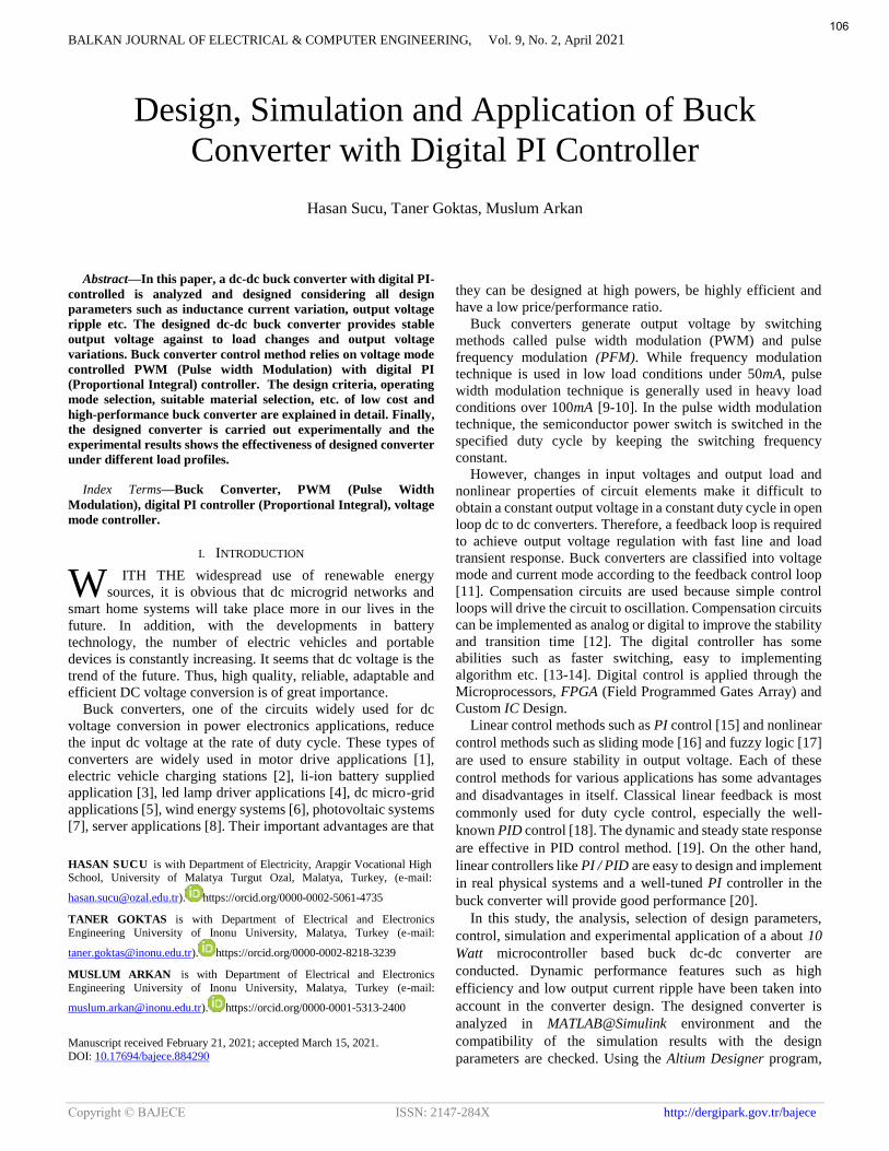
The basic circuit diagram for the dc-dc buck converter with
an output voltage lower than the input voltage is shown in Fig.1.
In the first stage of the design, it is necessary to determine the
operating modes and circuit parameters. As it is known, in
switching mode converters operate continuously,
discontinuously and in threshold conditions depending on
whether the inductance current falls to zero or not. Since the
inductance current does not decrease to zero in a converter
operating in a continuous current mode, the output-inductance
current ripple may be at a lower value compared to other
operating modes. In the discontinuous current mode, it has
advantages in terms of absorbing the energy in inductance,
especially at high powers.
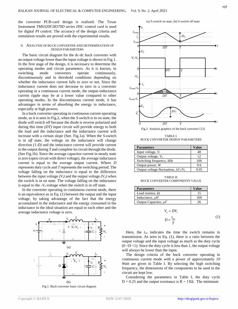
In a buck converter operating in continuous current operating
mode, as it is seen in Fig.2, when the S-switch is in on state, the
diode will switch off because the diode is reverse polarized and
during this time (DT) input circuit will provide energy to both
the load and the inductance and the inductance current will
increase with a certain slope (See. Fig.1a). When the S-switch
is in off state, the voltage on the inductance will change
direction (1-D) and the inductance current will provide current
to the output during T and complete its circuit through the diode.
(See Fig.1b). Since the average capacitor current in steady state
is zero (open circuit with direct voltage), the average inductance
current is equal to the average output current. Where D
represents duty cycle and T represents the switching period. The
voltage falling on the inductance is equal to the difference
between the input voltage (Vi) and the output voltage (Vo) when
the switch is in on state. The voltage falling on the inductance
is equal to the -Vo voltage when the switch is in off state.
In the converter operating in continuous current mode, there
is an equivalence as in Eq. (1) between the output and the input
voltage, by taking advantage of the fact that the energy
accumulated in the inductance and the energy consumed in the
inductance in the ideal situation are equal to each other and the
average inductance voltage is zero.
LS
Vi D C
RVo
+ Vi-Vo -
iL io
iC
ii +
-
LS
Vi
D C
RVo
- Vo +
iL io
iC +
-
(a)
(b) Fig.1. Buck converter basic circuit diagram
(a) S-switch on state, (b) S-switch off state
0
0
t
t
DT
DT
T
T
iL
iLmax
ΔiL
VL
iLmin
Vi-Vo
-Vo
0
0
t
t
DT
DT T
T
ic
iLmax-io
iLmin-io
Vo
ΔVo
Li
oV
ΔQ
Fig.2. Analysis graphics of the buck converter [12]
TABLE I. BUCK CONVERTER DESİGN PARAMETERS
Parameters Value
Input voltage, Vi 48
Output voltage, Vo 12
Switching frequency, kHz 100
Output power, W 9.6
Output voltage fluctuation, ∆Vo/Vo 0.05
TABLE II.
BUCK CONVERTER COMPONENTS VALUE
Parameters Value
Load resistor, Ω 15
Inductance, µH 100
Output Capacitor, µF 26
o i
on
V DV
tD
T
(1)
Here, the ton indicates the time the switch remains in
transmission. As seen in Eq. (1), there is a ratio between the
output voltage and the input voltage as much as the duty cycle
(0 <D <1). Since the duty cycle is less than 1, the output voltage
will always be lower than the input.
The design criteria of the buck converter operating in
continuous current mode with a power of approximately 10
Watt are given in Table I. By selecting the high switching
frequency, the dimensions of the components to be used in the
circuit are kept low.
Considering the parameters in Table I, the duty cycle
D = 0.25 and the output resistance is R = 15Ω. The minimum
107
BALKAN JOURNAL OF ELECTRICAL & COMPUTER ENGINEERING, Vol. 9, No. 2, April 2021
Copyright © BAJECE ISSN: 2147-284X http://dergipark.gov.tr/bajece
inductance (Lmin) value required for the converter to operate in
continuous current mode can be calculated by Eq. (2) [21]:
min
(1- )56.25
2
D RL H
f (2)
A converter operating at Lmin value calculated in Eq. (2)
operates under threshold condition. A value slightly larger than
this specified value should be selected to operate in continuous
current mode. In the design, this value was increased by 25%
and the inductance value in Eq. (3) was determined.
min1.25 70.31L L H (3)
The inductance current ripples depends on the inductance
voltage and the inductance value. If the inductance current
ripple is calculated considering the time the switch remains in
conduction:
-1.28
oiV Vi DT AL L
(4)
Depending on this ripple amount (ΔiL), the maximum
inductance current and minimum inductance curret can be
easily calculated as in Eq. (5) and in Eq. (6) by considering the
inductance current waveform in Fig. 2.
max 1.442
L
L L
II AI
(5)
max 0.162
L
L L
II AI
(6)
Buck converter output voltage ripple should generally be less
than 1%. Since the inductance current ripples are also seen in
the capacitor current, the capacitor value that ensures the output
voltage ripple (∆V0 / V0) to be at the desired value can be
calculated as in Eq. (6) [20]:
0 20 0
1-26
8 ( / )
DC F
L V V f
(7)
The values calculated for the components to be used in the
circuit are combined in Table II.
Considering the circuit design criteria and design parameters,
the values of the elements used in the circuit in a basic buck
converter operating in continuous current mode were
determined. In the next section, closed loop control of the Buck
converter is explained.
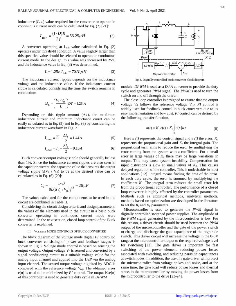
III. VOLTAGE MODE CONTROLS OF BUCK CONVERTER
The block diagram of the voltage mode digital PI controlled
buck converter consisting of power and feedback stages is
shown in Fig.3. Voltage mode control is based on sensing the
output voltage. Output voltage V0 is sensed and converted by a
signal conditioning circuit to a suitable voltage value for the
analog input channel and applied into the DSP via the analog
input channel. The sensed output voltage digitized by ADC is
compared with the reference voltage Vref. The obtained error
e[n] is tried to be minimized by PI control. The output K2e[n]
of this controller is used to generate duty cycle in DPWM
LS
Vi D C R Vo
iL io
iC
ii +
-
Gate Driver
DPWM PI A/D
Signal Conditioning
+K1V0[n]e[n]
Vref
K2e[n]
Digital Controller
Pwm K1V0
Fig.3. Digitally controlled buck converter block diagram
module. DPWM is used as a D / A converter to provide the duty
cycle and generates PWM signal. The PWM is used to turn the
switch on and off through the driver.
The close loop controller is designed to ensure that the output
voltage V0 follows the reference voltage Vref. PI control is
widely used for feedback control in buck converters due to its
easy implementation and low cost. PI control can be defined by
the following transfer function.
0
( ) ( ) ( )p iu t K e t K e d
(8)
Here u (t) represents the control signal and e (t) the error. Kp
represents the proportional gain and Ki the integral gain. The
proportional term aims to reduce the error by multiplying the
error coming from the system with a coefficient. For a small
error in large values of Kp there may be large variations in
output. This may cause system instability. Compensation for
input distortions is slow at small values of Kp. This causes
delayed regulation of the controller. This is undesirable in most
applications [12]. Integral means finding the area of the error.
In each duty cycle, the error is summed by multiplying the
coefficient Ki. The integral term reduces the small error left
from the proportional controller. The performance of a closed
loop converter is highly affected by the controller parameters.
Methods such as empirical methods, analytical methods,
methods based on optimization are developed in the literature
to set the Ki and Kp parameters.
Microcontroller is used to generate the PWM signal in
digitally controlled switched power supplies. The amplitude of
the PWM signal generated by the microcontroller is low. For
this reason, a driver circuit should be used between the PWM
output of the microcontroller and the gate of the power switch
to charge and discharge the gate capacitance of the high side
switch. This driver circuit will increase the voltage in the 0-5V
range at the microcontroller output to the required voltage level
for switching [22]. The gate driver is important for fast
switching of the power element, reducing power losses
associated with switching, and reducing parasitic capacitances
at switch nodes. In addition, the use of a gate driver will protect
the microcontroller from voltage spikes and noise, and at the
same time, the gate load will reduce power losses and thermal
stress in the microcontroller by moving the power losses from
the microcontroller to the drive [23-24].
108
BALKAN JOURNAL OF ELECTRICAL & COMPUTER ENGINEERING, Vol. 9, No. 2, April 2021
Copyright © BAJECE ISSN: 2147-284X http://dergipark.gov.tr/bajece
Driving techniques such as floating supply gate drive,
transformer coupled drive, charge pump drive, bootstrap drive
can be used in buck converters to switch the semiconductor
power switch [25-26]. However, the most appropriate solution
for driving semiconductor power switches in buck converters is
to use the bootstrap drive circuit in terms of cost and simplicity
[23].
IV. SIMULATION MODEL AND RESULTS
In order to verify the efficiency of the designed digitally
controlled buck converter, the Matlab @ Simulink model in
Fig.5. is created before its experimental implementation. The
simulation model has circuit parameters based on Table I and
Table II. The simulation model has been operated under full
load conditions, continuous current mode, closed loop control.
In the simulation model, suitable oscilloscopes are used to
observe the inductance current, inductance voltage, output
current, input and output voltages.
In the simulink model, the output voltage is detected and
compared to the 12V reference voltage. The obtained error is
tried to be minimized by PI control. PI control parameters Ki
and Kp can be determined using PID tuning tool in Matlab @
Simulink. Kp value is 0.02752 and Ki value is 8.1185. The
saturation block limits the error signal at the output of the PI
control to the upper and lower saturation values.The saturation
block output is compared with the sawtooth waveform
generated from the repeating sequence block to determine the
duty cycle. The frequency of the sawtooth waveform
corresponds to the desired converter switching frequency
100kHz. Mosfet switches when the error value is greater than
the triangular wave. With the step block, the switch is activated
0.03 seconds after the operating moment, the load of the circuit
is increased to 20W and the output voltage response of the
circuit against load changes is observed.
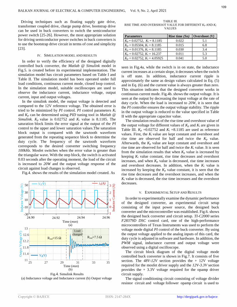
Fig.4. shows the results of the simulation model created. As
-10
10
30
50
24.90 24.92 24.94 24.96-30
Time (msn)
Time (msn)
(a)
(b)
iL(A)
25 27 29 31 33 3511
11.4
11.8
12.2
12.6
13
0
2
3
-1
1
VL(V)
V0(V)
Induct
or
Curr
ent
(A)
Induct
or
Volt
age
(V)
Outp
ut
Volt
age
(V) Load
changed
Rout=15 Rout=7.5
Fig.4. Simulink Results
(a) Inductance voltage and Inductance current (b) Output voltage
TABLE III.
RISE TIME AND OVERSHOOT VALUE FOR DIFFERENT KP AND Kİ VALUES
Parameters Rise time (Sn) Overshoot (V)
Kp = 0.02752, Ki = 8.1185 0.022 5.1
Kp = 0.05504, Ki = 8.1185 0.015 6.8
Kp = 0.01376, Ki = 8.1185 0.030 3.4
Kp = 0.02752, Ki = 16.237 0.011 5.3
Kp = 0.02752, Ki = 4.05925 0.041 5.0
seen in Fig.4a, while the switch is in on state, the inductance
current increases at a certain slope, it decreases when the switch
is off state. In addition, inductance current ripple is
approximately the same as design values calculated in Eq. (5)
and in Eq. (6) and the current value is always greater than zero.
This situation indicates that the designed converter works in
continuous current mode. Fig.4b. shows the output voltage. It is
seen at the output by decreasing the input voltage at the rate of
duty cycle. When the load is increased to 20W, it is seen that
the PI controller ensures the output voltage stability. The ripple
in the output voltage is reduced to the value specified in Table
II with the appropriate capacitor value.
The simulation results of the rise time and overshoot value of
the output voltage for different values of Kp and Ki are given in
Table III. Kp =0.02752 and Ki =8.1185 are used as reference
values. First, the Ki value are kept constant and overshoot and
rise time are observed for half and twice the Kp value.
Afterwards, the Kp value are kept constant and overshoot and
rise time are observed for half and twice the Ki value. It is seen
from the simulation results that when Kp value is increased by
keeping Ki value constant, rise time decreases and overshoot
increases, and when Kp value is decreased, rise time increases
and overshoot decreases. In addition, when the Ki value is
increased by keeping the Kp value constant, it is seen that the
rise time decreases and the overshoot increases, and when the
Ki value is decreased, the rise time increases and the overshoot
decreases.
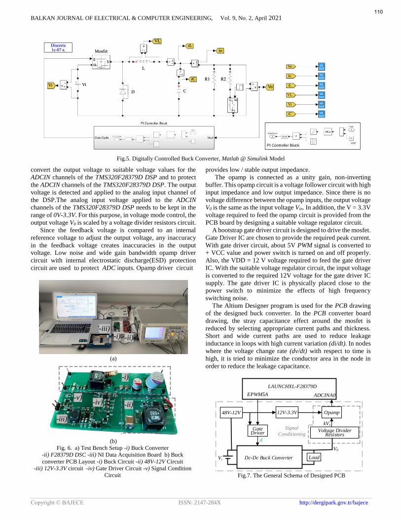
V. EXPERIMENTAL SETUP AND RESULTS
In order to experimentally examine the dynamic performance
of the designed converter, an experimental circuit setup
consisting of the input power source, the designed buck
converter and the microcontroller was established. Fig.6. shows
the designed buck converter and circuit setup. TI-C2000 series
F28379D DSC control card, one of the high-performance
microcontrollers of Texas Instruments was used to perform the
voltage mode digital PI control of the buck converter. By using
the output voltage applied to the analog inputs of this card, the
duty cycle is adjusted in software and hardware. In addition, the
PWM signal, inductance current and output voltage were
observed using a digital oscilloscope.
The circuit block diagram of the digital voltage mode
controlled buck converter is shown in Fig.7. It consists of five
section. The 48V-12V section provides the + 12V voltage
required for the mosfet driver supply and the 12V-3.3V section
provides the + 3.3V voltage required for the opamp driver
circuit supply.
The signal conditioning circuit consisting of voltage divider
resistor circuit and voltage follower opamp circuit is used to
109
BALKAN JOURNAL OF ELECTRICAL & COMPUTER ENGINEERING, Vol. 9, No. 2, April 2021
Copyright © BAJECE ISSN: 2147-284X http://dergipark.gov.tr/bajece
PI Controller BlockVref
Fig.5. Digitally Controlled Buck Converter, Matlab @ Simulink Model
convert the output voltage to suitable voltage values for the
ADCIN channels of the TMS320F28379D DSP and to protect
the ADCIN channels of the TMS320F28379D DSP. The output
voltage is detected and applied to the analog input channel of
the DSP.The analog input voltage applied to the ADCIN
channels of the TMS320F28379D DSP needs to be kept in the
range of 0V-3.3V. For this purpose, in voltage mode control, the
output voltage V0 is scaled by a voltage divider resistors circuit.
Since the feedback voltage is compared to an internal
reference voltage to adjust the output voltage, any inaccuracy
in the feedback voltage creates inaccuracies in the output
voltage. Low noise and wide gain bandwidth opamp driver
circuit with internal electrostatic discharge(ESD) protection
circuit are used to protect ADC inputs. Opamp driver circuit
-i) -ii)
-iii)
(a)
-i)
-ii)
-iii)
-iv)-v)
(b)
Fig. 6. a) Test Bench Setup -i) Buck Converter
-ii) F28379D DSC -iii) NI Data Acquisition Board b) Buck
converter PCB Layout -i) Buck Circuit -ii) 48V-12V Circuit
-iii) 12V-3.3V circuit -iv) Gate Driver Circuit -v) Signal Condition
Circuit
provides low / stable output impedance.
The opamp is connected as a unity gain, non-inverting
buffer. This opamp circuit is a voltage follower circuit with high
input impedance and low output impedance. Since there is no
voltage difference between the opamp inputs, the output voltage
V0 is the same as the input voltage Vin. In addition, the V = 3.3V
voltage required to feed the opamp circuit is provided from the
PCB board by designing a suitable voltage regulator circuit.
A bootstrap gate driver circuit is designed to drive the mosfet.
Gate Driver IC are chosen to provide the required peak current.
With gate driver circuit, about 5V PWM signal is converted to
+ VCC value and power switch is turned on and off properly.
Also, the VDD = 12 V voltage required to feed the gate driver
IC. With the suitable voltage regulator circuit, the input voltage
is converted to the required 12V voltage for the gate driver IC
supply. The gate driver IC is physically placed close to the
power switch to minimize the effects of high frequency
switching noise.
The Altium Designer program is used for the PCB drawing
of the designed buck converter. In the PCB converter board
drawing, the stray capacitance effect around the mosfet is
reduced by selecting appropriate current paths and thickness.
Short and wide current paths are used to reduce leakage
inductance in loops with high current variation (di/dt). In nodes
where the voltage change rate (dv/dt) with respect to time is
high, it is tried to minimize the conductor area in the node in
order to reduce the leakage capacitance.
Vi
kVo
Gate Driver
Voltage Divider Resistors
LoadDc-Dc Buck Converter
LAUNCHXL-F28379D
EPWM5A ADCINA0
Opamp
V0
Signal
Conditioningd
48V-12V 12V-3.3V
Fig.7. The General Schema of Designed PCB
110
BALKAN JOURNAL OF ELECTRICAL & COMPUTER ENGINEERING, Vol. 9, No. 2, April 2021
Copyright © BAJECE ISSN: 2147-284X http://dergipark.gov.tr/bajece
(a) (a)
(b) (b)
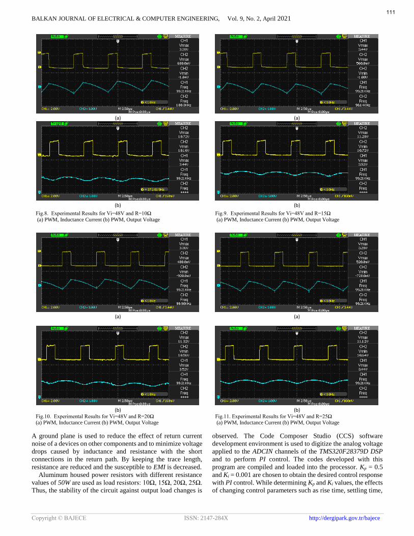
Fig.8. Experimental Results for Vi=48V and R=10Ω
(a) PWM, Inductance Current (b) PWM, Output Voltage
Fig.9. Experimental Results for Vi=48V and R=15Ω
(a) PWM, Inductance Current (b) PWM, Output Voltage
(a) (a)
(b) (b)
Fig.10. Experimental Results for Vi=48V and R=20Ω (a) PWM, Inductance Current (b) PWM, Output Voltage
Fig.11. Experimental Results for Vi=48V and R=25Ω (a) PWM, Inductance Current (b) PWM, Output Voltage
A ground plane is used to reduce the effect of return current
noise of a devices on other components and to minimize voltage
drops caused by inductance and resistance with the short
connections in the return path. By keeping the trace length,
resistance are reduced and the susceptible to EMI is decreased.
Aluminum housed power resistors with different resistance
values of 50W are used as load resistors: 10Ω, 15Ω, 20Ω, 25Ω.
Thus, the stability of the circuit against output load changes is
observed. The Code Composer Studio (CCS) software
development environment is used to digitize the analog voltage
applied to the ADCIN channels of the TMS320F28379D DSP
and to perform PI control. The codes developed with this
program are compiled and loaded into the processor. Kp = 0.5
and Ki = 0.001 are chosen to obtain the desired control response
with PI control. While determining Kp and Ki values, the effects
of changing control parameters such as rise time, settling time,
111

BALKAN JOURNAL OF ELECTRICAL & COMPUTER ENGINEERING, Vol. 9, No. 2, April 2021
Copyright © BAJECE ISSN: 2147-284X http://dergipark.gov.tr/bajece
overshoot, steady state error and stability are taken into
consideration.
Fig.8, Fig.9, Fig.10. and Fig.11. shows the experimental
results for different load resistance with Vi =48V. The
amplitude of the switching signal produced by TI-F28379D is
about 3.3V. Switching frequency is 100kHz. This generated
switching signal is connected to the power mosfet gate driver
circuit as an input. As seen in Fig.8(a), Fig.9(a), Fig.10(a) and
Fig.11(a), inductance current ripple match calculated values
and Simulink results. Inductance currents are 1.044A, 0.733A,
0.547A and 0.435A for 10Ω, 15Ω, 20Ω, 25Ω resistors,
respectively. When the inductance current waveforms are
examined carefully, it is seen that the converter operates in
continuous current mode. The output voltage contains only a
small ripple caused by the parasitic parameters in the converter.
As seen in Fig.8(b), Fig.9(b), Fig.10(b) and Fig.11(b),
measurements show an under/overshoot voltage of -0.38V. The
output voltage ripple is within permissible limit. In addition, the
converter is stable, working at a switching frequency of 100
kHz without significant noise.
It is seen from the experimental results that the average
values of output voltages are almost the same for all load
resistance. The designed controller sets the duty cycle
depending on load resistance.
Fig.12. shows the thermal performance of designed converter
with 15Ω load resistor. This snapshot is taken at 250C ambient
temperature. The section of the PCB with the maximum heat is
shown in red. This section includes a low power 1Ω resistor
used to measure inductance current. This resistor is not included
in the designed circuit and is added just before measurement.
The yellow portion indicates the heat on inductance.
In order to calculate the efficiency of the circuit, the
experimental results measured with a multimeter are given in
Table IV. The input power is calculated as 8.92 W and the
output power is 7.657W. The power efficiency is calculated as
follow:
0% 100 85.8İ
P
P (9)
As seen, the efficiency of the system is lower than 100% due
to on-state resistances of mosfet and diode.
20 0C
35 0C
30 0C
25 0C
40 0C
45 0C
50 0C
Fig.12. Thermal performance of designed converter
TABLE IV.
BUCK CONVERTER EXPERİMENTAL RESULTS
Parameters Value
Input voltage, V 48.22
Input current, A 0.185
Output voltage, V 11
Output current, A 0.696
VI. CONCLUSION
In this study, the analysis, simulation and experimental
application of a microcontroller-based dc-dc buck converter is
carried out. The architecture and circuit implementation details
are discussed in detail. The design parameters are verified with
simulations and experiments. It is observed that the designed
converter provides important design criteria such as high
operating frequency, low output current ripple, and continuous
current mode. Closed loop control technique is applied to the
designed converter to hold the output voltages constants against
to the load changes. The presented simulation and experimental
results show the effectiveness of the developed controller in
terms of overshoot limitations and accuracy.
REFERENCES
[1] A. A. A. Ismail and A. Elnady, "Advanced Drive System for DC Motor
Using Multilevel DC/DC Buck Converter Circuit," in IEEE Access, vol.
7, pp. 54167-54178, 2019. [2] S. Kamat and S. Jadhav, "Design and Simulation of Low Power Charging
Station for Electric Vehicle," 2019 International Conference on Advances
in Computing, Communication and Control (ICAC3), Mumbai, India, 2019, pp. 1-4.
[3] K. Hu, Y. Chen, H. Lin and C. Tsai, "Digital Buck Converter with Adaptive Driving Circuit for Cascode Power MOS," 2018 IEEE 7th
Global Conference on Consumer Electronics (GCCE), Nara, 2018, pp.
126-127. [4] R. T. Yadlapalli and A. Kotapati, "Efficieny analysis of Quadratic buck
converter for LED lamp driver applications," 2017 International
Conference on Trends in Electronics and Informatics (ICEI), Tirunelveli, 2017, pp. 210-214.
[5] N. Rigogiannis et al., "Experimental Investigation of a Digitally Current
Controlled Synchronous Buck DC/DC Converter for Microgrids Applications," 2019 Panhellenic Conference on Electronics &
Telecommunications (PACET), Volos, Greece, 2019, pp. 1-5.
[6] A. A. Patil, et al,, "Output voltage control scheme for standalone wind energy system," 2016 Int. Conf. on Computation of Power, Energy
Information and Com. Chennai, 2016, pp. 534-541.
[7] K. Pal and M. Pattnaik, "Performance of a Synchronous Buck Converter for a Standalone PV System: an Experimental Study," 2019 IEEE 1st
International Conference on Energy, Systems and Information Processing
(ICESIP), Chennai, India, 2019, pp. 1-6. [8] C. Fei, M. H. Ahmed, F. C. Lee and Q. Li, "Two-Stage 48 V-12 V/6 V-
1.8 V Voltage Regulator Module With Dynamic Bus Voltage Control for
Light-Load Efficiency Improvement," in IEEE Transactions on Power Electronics, vol. 32, no. 7, pp. 5628-5636, July 2017.
[9] Y. Chen, J. Chen and D. Lai, "Dual mode digital buck converter controller
without current sensor," 2018 IEEE International Conference on Industrial Electronics for Sustainable Energy Systems (IESES),
Hamilton, 2018, pp. 118-123.
[10] J. Yu, I. Hwang and N. Kim, "High performance CMOS integrated PWM/PFM dual-mode DC-DC buck converter," 18th Int. Scientific Conf.
on Electric Power Engineering (EPE), Kouty nad Desnou, 2017, pp. 1-4.
[11] Y. Moursy, R. Khalil, S. Lecce, V. Poletto, R. Iskander and M. Louërat,
"Mixed-signal PI controller in current-mode DC-DC buck converter for
automotive applications," 2016 IEEE International Symposium on
Circuits and Systems (ISCAS), Montreal, QC, 2016, pp. 1610-1613. [12] A. Platon, S. Oprea, A. Florescu and S. G. Rosu, "Simple and Digital
Implementation of PI Controller Used in Voltage-Mode Control," 2018
10th International Conference on Electronics, Computers and Artificial Intelligence (ECAI), Iasi, Romania, 2018, pp. 1-6.
[13] Q. Huang, C. Zhan and J. Burm, "A 4-MHz Digitally Controlled Voltage-
Mode Buck Converter With Embedded Transient Improvement Using Delay Line Control Techniques," in IEEE Transactions on Circuits and
Systems I: Regular Papers, vol. 67, no. 11, pp. 4029-4040, Nov. 2020.
[14] Y. Yan, A. Shehada, A. R. Beig and I. Boiko, "Auto-Tuning of PID Controller with Phase Margin Specification for Digital Voltage-Mode
Buck Converter," 2020 IEEE Conference on Control Technology and
Applications (CCTA), Montreal, QC, Canada, 2020, pp. 801-806. [15] P. Suskis and D. Nikonorov, "Buck Converter Digital Control System
Design and Performance Evaluation," 2018 IEEE 6th Workshop on
112

BALKAN JOURNAL OF ELECTRICAL & COMPUTER ENGINEERING, Vol. 9, No. 2, April 2021
Copyright © BAJECE ISSN: 2147-284X http://dergipark.gov.tr/bajece
Advances in Information, Electronic and Electrical Engineering (AIEEE),
Vilnius, 2018, pp. 1-4. [16] M. Deshmukh and M. K. Namboothiripad, "DSP BasedSecond Order
Sliding Mode Controller for Buck Converter," 2018 3rd International
Conference for Convergence in Technology (I2CT), Pune, 2018, pp. 1-5. [17] M. K. Asy’ari, A. Musyafa’ and K. Indriawati, "Design of Wind Turbine
Output Voltage Control Systems in Multi-Input Buck Converter Using
Fuzzy Logic Control for Battery Charging," 2019 Int. Conference on Advanced Mechatronics, Intelligent Manufacture and Industrial
Automation (ICAMIMIA), Batu, Malang, Indonesia, 2019, pp. 249-252.
[18] S. Seshagiri, E. Block, I. Larrea and L. Soares, "Optimal PID design for voltage mode control of DC-DC buck converters," 2016 Indian Control
Conference (ICC), Hyderabad, 2016, pp. 99-104.
[19] S. Ghosh, S. Satpathy, S. Das, S. Debbarma and B. K. Bhattacharyya,"Different Controlling Method of Closed Loop DC-DC Buck Converter:
A review," 2018 International Conference on Smart Systems and
Inventive Technology (ICSSIT), Tirunelveli, India, 2018, pp. 29-33. [20] M. M. Garg, Y. V. Hote, M. K. Pathak and L. Behera, "An Approach for
Buck Converter PI Controller Design Using Stability Boundary Locus,"
2018 IEEE/PES Transmission and Distribution Conference and Exposition (T&D), Denver, CO, 2018, pp. 1-5.
[21] Daniel W. Hart., “Power Electronics”, McGraw-Hill, New York-
Americas, 2011 [22] B. Yuan, J. Ying, W. T. Ng, X. Lai and L. Zhang, "A High-Voltage DC–
DC Buck Converter With Dynamic Level Shifter for Bootstrapped High-
Side Gate Driver and Diode Emulator," in IEEE Transactions on PowerElectronics, vol. 35, no. 7, pp. 7295-7304, July 2020.
[23] Design and Evaluation of A High-Current Gate Driver Circuit for Six Paralleled 1.2kV 36A SiC MOSFETs
[24] “UCC27211A-Q1 120V Boot, 4A Peak, High Frequency High Side and
Low Side Driver,” SLUSCG0A datasheet, 2015[25] MH Rashid, “Power Electronics Circuits, Devices and Applications”, 3rd
Ed.,Prentice-Hall, 2003, pp 761~789
[26] Fairchild Application Note AN-6076 : Design and Application Guide of Bootstrap Circuit for High Voltage Gate Drive IC.
BIOGRAPHIES
HASAN SUCU received B.S. degrees in electrical
engineering from İnonu University, Malatya, Turkey, in 2009. Since 2018, he has been a student
of B.S. degree in Inonu University, Malatya, in the
Electrical and Electronics Engineering department. He is currently with the Arapgir Vocational High
School, Electric Program, Malatya Turgut Ozal
University, Malatya, Turkey. His research interests include design of dc-dc converters and power
electronics circuits.
TANER GOKTAS received B.S and M.S degrees in electrical engineering from Firat University,
Elazig, Turkey, in 2006 and 2010, respectively,
and the Ph.D. degree in Electrical Engineering from the Inonu University, Malatya, Turkey, in
2015. He was a visiting scholar in the Power Electronic and Drives Lab, University of Texas at
Dallas from 2014 to 2015. Since 2016, he has been
with Inonu University as an Assistant Professor.
His research interests include electric machines
drives, power electronics, condition monitoring, motor design and diagnostic
techniques in electric machines.
MUSLUM ARKAN received B.Sc. degree in
Electrical and Electronics Engineering from
University of Gaziantep, Turkey and his Ph. D. degree in Electrical Engineering from University of
Sussex, Brighton, UK, in 1994 and 2000
respectively. Since 1994, he has been with the Electrical and Electronics Engineering Department,
Inonu University, Malatya, Turkey, where he is
currently a full Professor. His research activities include the use of digital signal analysis for
diagnostic, condition monitoring and motor failure
prediction by sensorless methods and modeling of electrical machines for diagnosis purpose.
113