basics of electrostatic discharge protection · prof. mayank shrivastava, dese, iisc 1 basics of...
TRANSCRIPT
20-11-2013
Prof. Mayank Shrivastava, DESE, IISc 1
Basics of Electrostatic Discharge
(ESD) Protection
Prof. Mayank Shrivastava
Department of Electronic Systems Engineering
Indian Institute of Science Bangalore
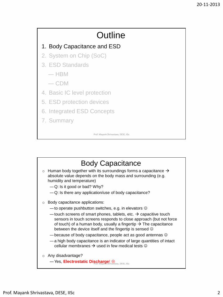
Outline 1. Body Capacitance and ESD
2. System on Chip (SoC)
3. ESD Standards
― HBM
― CDM
4. Basic IC level protection
5. ESD protection devices
6. Integrated ESD Concepts
7. Summary
Prof. Mayank Shrivastava, DESE, IISc
20-11-2013
Prof. Mayank Shrivastava, DESE, IISc 2
Outline 1. Body Capacitance and ESD
2. System on Chip (SoC)
3. ESD Standards
― HBM
― CDM
4. Basic IC level protection
5. ESD protection devices
6. Integrated ESD Concepts
7. Summary
Prof. Mayank Shrivastava, DESE, IISc
o Human body together with its surroundings forms a capacitance
absolute value depends on the body mass and surrounding (e.g.
humidity and temperature)
―Q: Is it good or bad? Why?
―Q: Is there any application/use of body capacitance?
o Body capacitance applications:
― to operate pushbutton switches, e.g. in elevators
― touch screens of smart phones, tablets, etc. capacitive touch
sensors in touch screens responds to close approach (but not force
of touch) of a human body, usually a fingertip The capacitance
between the device itself and the fingertip is sensed
―because of body capacitance, people act as good antennas
―a high body capacitance is an indicator of large quantities of intact
cellular membranes used in few medical tests
o Any disadvantage?
―Yes, Electrostatic Discharge!
Body Capacitance
Prof. Mayank Shrivastava, DESE, IISc
20-11-2013
Prof. Mayank Shrivastava, DESE, IISc 3
++
++
++
++
Electrostatic Discharge (ESD)
RDUT
CSUBRSUB
PAD
Discharge Path o Charge can be stored or
accumulated across physical
bodied (if isolated from
ground)
o It can be a human body, a
machine or the electronic
equipment (e.g. IC) itself
(In general) ESD is the transfer of electrostatic charge between
bodies (or surfaces) at different electrostatic potential
Electrical Overstress (EOS): Exposure of an object to current or voltage
beyond its physical limits (max. ratings). ESD is a subject of EOS.
Prof. Mayank Shrivastava, DESE, IISc
ESD EOS Specific Lightning
- High Voltage (1V –15kV)
- Short Duration (< 1ms)
- Very Low Power
- Low Rise Time (1-10ns)
- Low Voltage
- Longer Duration (> 1ms)
- Low Power
- High Rise Time (~ 10ms)
- Extremely High Voltage
- Extremely High Power
EOS In-General
ICs used in automotive, military,
medical, consumer, etc. electronics
can be damaged with ESD and EOS
Houses, Buildings
Airplanes, Electronics,
etc.
ESD Regime EOS Regime
Pf (L
og)
tf (Log)
~ 𝑡𝑓−1
~ 𝑡𝑓−1/2
~1
log(𝑡𝑓)
~ 𝑡𝑓−1
~ 𝑡𝑓−1/2
~1
log(𝑡𝑓)
~1
log(𝑡𝑓)
Constant Power
Dwyer, SSE, 1990 (modified)
o ESD: Heat does not disperse
much localized failures
o EOS: Wide spreading of heat
large areas of damage
Prof. Mayank Shrivastava, DESE, IISc

20-11-2013
Prof. Mayank Shrivastava, DESE, IISc 4
Grounding Person
Wrist Strap to Ground
(or flooring/footwear)
1
Grounded Work Surface
2
ESD Protective
Packaging
3
ESD for Layman
Prof. Mayank Shrivastava, DESE, IISc
ESD: Factory Measures
System Level ESD IC Level ESD
Prof. Mayank Shrivastava, DESE, IISc
20-11-2013
Prof. Mayank Shrivastava, DESE, IISc 5
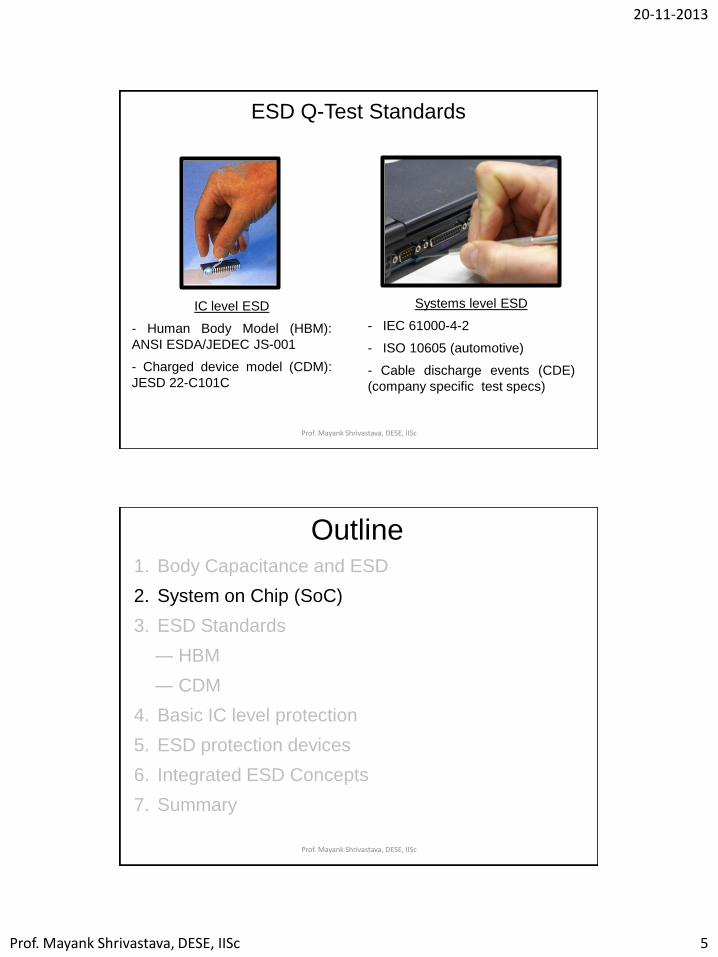
ESD Q-Test Standards
IC level ESD
- Human Body Model (HBM):
ANSI ESDA/JEDEC JS-001
- Charged device model (CDM):
JESD 22-C101C
Systems level ESD
- IEC 61000-4-2
- ISO 10605 (automotive)
- Cable discharge events (CDE)
(company specific test specs)
Prof. Mayank Shrivastava, DESE, IISc
Outline 1. Body Capacitance and ESD
2. System on Chip (SoC)
3. ESD Standards
― HBM
― CDM
4. Basic IC level protection
5. ESD protection devices
6. Integrated ESD Concepts
7. Summary
Prof. Mayank Shrivastava, DESE, IISc

20-11-2013
Prof. Mayank Shrivastava, DESE, IISc 6
CPU v/s SoC Products
PC Client Data
Center
CPU
Netbook &
Tablet
Smart
Phones Embedded
Consumer
Electronics Wireless
SoC
Prof. Mayank Shrivastava, DESE, IISc
Progress in SoC Integration
2012
5.
PA
2008
4.
FM Radio
2006
3.
Power
Manage-
ment Unit
2005
2.
RF Trans-
ceiver
2000
1.
Digital
Baseband Analog
Baseband
Prof. Mayank Shrivastava, DESE, IISc
20-11-2013
Prof. Mayank Shrivastava, DESE, IISc 7
Outline 1. Body Capacitance and ESD
2. System on Chip (SoC)
3. ESD Standards
― HBM
― CDM
4. Basic IC level protection
5. ESD protection devices
6. Integrated ESD Concepts
7. Summary
Prof. Mayank Shrivastava, DESE, IISc
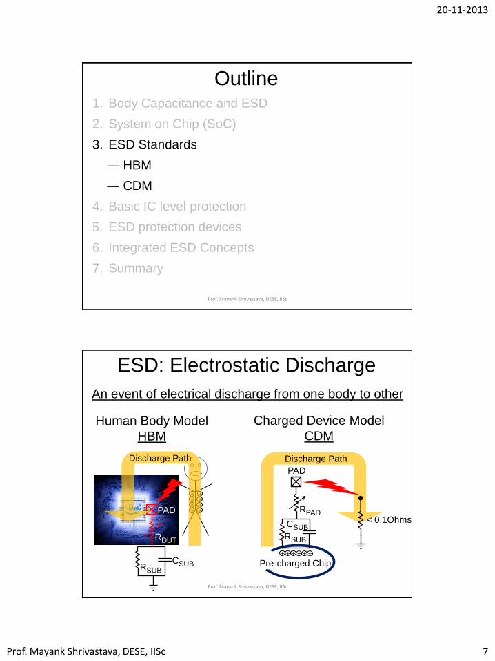
ESD: Electrostatic Discharge
An event of electrical discharge from one body to other
Discharge Path
+ + + + + +
Pre-charged Chip
RPAD
CSUB
RSUB
PAD
< 0.1Ohms
Charged Device Model
CDM
RDUT
CSUB RSUB
PAD
+ +
+ +
+ +
+ +
Human Body Model
HBM
Discharge Path
Prof. Mayank Shrivastava, DESE, IISc

20-11-2013
Prof. Mayank Shrivastava, DESE, IISc 8
0 100 200 300 400 500
0.0
0.3
0.6
0.9
1.2
Curr
ent
(A)
Time (ns)
Stress (& test) Models HBM: Human Body Model
Rise Time = 10ns
Peak Current = 1.3A
Av. Stress time = 100ns
Target = 2KV
RHBM = 1.5KΩ
C CHBM = 100pF
L
DUT (RL)
Human Body
Tester parasitic
L: Parasitic inductance
C: Test board capacitance
RL=0
Prof. Mayank Shrivastava, DESE, IISc
0 200 400 600
0
2
4
6
8
10
Curr
ent
(A)
Time (ps)
Stress (& test) Models….cont.
Rise Time = 100ps
Peak Current = 10A
Av. Stress time = 0.5ns
Target = 500V
CDM: Charged Device Model
Field Plate
Insulator
50 co-ax
Pogo Pin
DUT
GND Plate
HV
Supply
>100M
Prof. Mayank Shrivastava, DESE, IISc

20-11-2013
Prof. Mayank Shrivastava, DESE, IISc 9
Charged Device Model (CDM)– Test Setup
Prof. Mayank Shrivastava, DESE, IISc
ESD Waveforms
[Gieser] (modified)
1-16A~3.6A1.33APeak Current
100-500ps10-15ns2-10nsRise Time
~1ns~40ns~150nsPulse Width
500V200V2kVQual levels
CDMMMHBMModel
1-16A~3.6A1.33APeak Current
100-500ps10-15ns2-10nsRise Time
~1ns~40ns~150nsPulse Width
500V200V2kVQual levels
CDMMMHBMModel
-3
0
3
6
9
12
0 20 40 60 80 100 120
Time, t (ns)
Dis
charg
e C
urr
ent, I
ES
D(A
)
500V CDM
2000V HBM
200V MM
Typical CDM
peak current
range
15
o CDM discharge leads to very high, short current spikes
o ESD protection must limit excess voltage at gate oxides
due to high current Prof. Mayank Shrivastava, DESE, IISc

20-11-2013
Prof. Mayank Shrivastava, DESE, IISc 10
ESD Device characterization: Transmission Line Pulsing
Device characterization with rectangular pulses which are
generated by a Transmission Line Pulser (TLP)
HV
0 - Mega Ohms
50 transmission
line (e.g. 5m)
DUT
Switch
0
0.5
1
1.5
2
1 2 3 4
curr
ent [A
]
voltage [V]
I-V data point
Vhold
Vt1
It2
Vt2
0
0.2
0.4
0.6
0.8
1
1.2
1.4
-20 0 20 40 60
curr
ent [A
]
time [ns]
averaged
current
0
1
2
3
4
5
6
-20 0 20 40 60volta
ge
[V
]
time [ns]
averaged
voltage
Voltage probe
Current probe
Prof. Mayank Shrivastava, DESE, IISc
ESD Consequences
VDD
VSS
I/P
PAD
Internal
Circuit
VDD
VSS
O/P
PAD
-
+
-
+
Prof. Mayank Shrivastava, DESE, IISc

20-11-2013
Prof. Mayank Shrivastava, DESE, IISc 11
Failure Mechanism Failure: Device
Level
Failure: System
Level
Oxide Breakdown
(Left: Gate Oxide
Right: LOCOS)
Thermal Melting
(Left: Silicon
Right: Metal)
o CDM type fails causes breakdown of thin dielectrics
o HBM type fails causes thermal fails of silicon device or weak interconnects
o System level ESD or EOS causes much more extended fails
Physical Failure Signature
Outline 1. Body Capacitance and ESD
2. System on Chip (SoC)
3. ESD Standards
― HBM
― CDM
4. Basic IC level protection
5. ESD protection devices
6. Integrated ESD Concepts
7. Summary
Prof. Mayank Shrivastava, DESE, IISc

20-11-2013
Prof. Mayank Shrivastava, DESE, IISc 12
(Simplified) ESD protection
-
VDD
VSS
I/P
PAD
Internal
Circuit
VDD
VSS
O/P
PAD
ESD
ESD
ESD
ESD
+
-
+
(unwanted)
Voltage Drop
(unwanted)
Current Path
Tradeoffs: ESD robustness vs.
Circuit level System/IC level
Area Yield and cost
Leakage Design time/cycle
Performance Time to market
Complexity and design difficulty Testing and qualification requirements Prof. Mayank Shrivastava, DESE, IISc
ESD Design Window
o ESD design space is governed by:
― thermal failure limits (second breakdown)
― reliability constraints (dielectric breakdown)
o ESD design space is limited by:
― shrinking technology
― interconnect resistance and capacitive loading Prof. Mayank Shrivastava, DESE, IISc
20-11-2013
Prof. Mayank Shrivastava, DESE, IISc 13
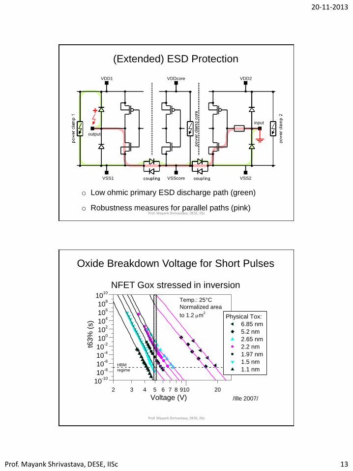
(Extended) ESD Protection
VDD1
VSS1
output
VDD2
input
VSS2VSScore
VDDcore
+
o Low ohmic primary ESD discharge path (green)
o Robustness measures for parallel paths (pink) Prof. Mayank Shrivastava, DESE, IISc
Oxide Breakdown Voltage for Short Pulses
2 3 4 5 6 7 8 910 20
10-10
10-8
10-6
10-4
10-2
100
102
104
106
108
1010
Physical Tox:
6.85 nm
5.2 nm
2.65 nm
2.2 nm
1.97 nm
1.5 nm
1.1 nm
Temp.: 25°C
Normalized area
to 1.2 mm2
t63
% (
s)
Voltage (V)
HBM
regime
NFET Gox stressed in inversion
/Ille 2007/
Prof. Mayank Shrivastava, DESE, IISc

20-11-2013
Prof. Mayank Shrivastava, DESE, IISc 14
Rail-based ESD protection VDD
VSS
pad
pow
er
cla
mp
pow
er
cla
mp
-
driver
sta
ge
VDD
VSS
pad
pow
er
cla
mp
pow
er
cla
mp
+
driver
sta
ge
o Shunt ESD current over (ESD
+ parasitic) diode and power
clamp in series
Power clamp:
low trigger voltage
low on-resistance
low leakage
low latchup immunity
Immunity to power ramp
Low ohmic metal routing
o Protect driver stage
Avoid turn-on
Limit current through
driver
Ingredients:
Power clamp (mostly RC-triggered MOS)
PAD-to-VSS & PAD-to-VDD clamps (often
special ESD diodes are used) Prof. Mayank Shrivastava, DESE, IISc
Local Clamp ESD Protection VDD
VSS
pad
pow
er
cla
mp
pow
er
cla
mp
-
driver
sta
ge
ES
DV
SS
ES
DV
DD
VDD
VSS
pad
pow
er
cla
mp
pow
er
cla
mp
+
driver
sta
ge
ES
DV
SS
ES
DV
DD o Shunt ESD current over
primary ESD protection
element (or parasitic
diode)
o Protect driver stage
avoid turn-on
limit current through
driver
Ingredients:
Power clamp (RC-triggered MOS only for low
voltage domains)
PAD-to-VSS & PAD-to-VDD local clamps (ESD
diodes are not used directly) Prof. Mayank Shrivastava, DESE, IISc

20-11-2013
Prof. Mayank Shrivastava, DESE, IISc 15
Comparison of Protection Concepts
o Rail-based concepts with RC triggered power clamps most
beneficial for large digital domains without overvoltage
requirements
Caveat: Verify comptibility of fastest ramp-time of supply
voltage with turn-on of power clamp
o Local clamps efficient for
RF IOs with critical ESD design window
(e.g. LNA with thin Gox gate)
Overvoltage tolerant IOs
(I2C, USB, ...)
Failsafe IOs
Domains with very low IDDQ requirements (order of 10
nA @ RT) Prof. Mayank Shrivastava, DESE, IISc
VDD
VSS
I/P
PAD
Internal
Circuit
(unwanted)
Voltage Drop
IESD
IESD
-
+
Primary
ESD clamp
Voltage Shunt
VESD
VESD
1K
Secondry
ESD clamp
ESD Protection for Digital Inputs
o Protection required for
(thin) gate oxides
o ESD tradeoff:
Area
Speed
I/P matching for
RF IOs Prof. Mayank Shrivastava, DESE, IISc

20-11-2013
Prof. Mayank Shrivastava, DESE, IISc 16
Outline 1. Body Capacitance and ESD
2. System on Chip (SoC)
3. ESD Standards
― HBM
― CDM
4. Basic IC level protection
5. ESD protection devices
6. Integrated ESD Concepts
7. Summary
Prof. Mayank Shrivastava, DESE, IISc
Basic ESD Protection elements and Power
Clamp
DIODE
Use only in Forward Bias
SCR
Power clamp & local clamp
Be aware of turn-on delay and latching
RCMOS
Power clamp
Be aware of false triggering
R
MOS C
Prof. Mayank Shrivastava, DESE, IISc

20-11-2013
Prof. Mayank Shrivastava, DESE, IISc 17
Gate-Controlled MOS Clamp (“RCMOS”)
0
1
2
3
4
5
0 1 2 3 4 5
cla
mp
cu
rre
nt
[A]
VDD voltage [V]
o Clamp is quickly turned on by gate biasing large NMOS, excellent
clamping characteristics
o Clamp turned off after RC-timeout, ESD needs to be over by then!
o Typical application: supply rail clamping (i.e. not for local clamping)
o Full circuit simulation possible, no special models required
o Challenges: stand-by leakage during normal IC operation, unintended
turn-on during power ramp-up and tendency to oscillations!
R
C
VDD
Large
(N)MOS
e.g.
W=2000um
VSS
IO circuitRCMOS or BigFET clamp
Prof. Mayank Shrivastava, DESE, IISc
Design of RCMOS Power Clamp
– goal #1: no triggering for slow ramps
(1ms)
o R1 * C1 < 1ms
– goal #2: no early time out during ESD
o R1 * C1 > 0.5ms
– example:
o C1 ≈ 3pF, R1 ≈ 200kΩ
– Outside SOA: risk of false triggering / early
time out
– simplification: C1 >> CP1+CN1
VDD
Note: This is a simplified
design. Many complex
designs are available in
literature.
Prof. Mayank Shrivastava, DESE, IISc

20-11-2013
Prof. Mayank Shrivastava, DESE, IISc 18
ESD Diodes
0
0.5
1
1.5
0 1 2 3 4
STI
diodeGated
diode
curr
ent
[A]
voltage [V]
width =
50um
It2
It2
IV-Characteristics
o STI diodes: voltage overshoot due to strong forward recovery effect
o Gated diodes ( and NonSTI-diodes w/o gate)
much lower Ron and higher It2 for same device size
far less voltage overshoot makes them superior for ESD applications!
-1
0
1
2
3
4
5
6
-1 0 1 2 3 4
STI diodeGated diode
vo
lta
ge [
V]
time [ns]
width = 50um
I = 0.5A
oxide damage!
Transient response
N+ P+
C A
curved current flow
LstiS
TI
STI Diode
N+ P+
Nwell
Psub
gate
ST
I
C A
direct
current flow
Lg
Gated Diode
Prof. Mayank Shrivastava, DESE, IISc
Silicon Controlled Rectifier (SCR)
voltage
Itri
gg
er
Vtrig
X-section equivalent circuit
selected trigger devices o Basic structure shown; many options
o Internal spacing Lac and process
conditions determine holding voltage
and speed
o Intrinsic latchup-danger can be addressed
by e.g. series diodes
IV + latchup
PNP
NPN
Anode
Well
SUB
Itrigger
Rsub
(series diodes)
N+
Cathode
P+
SUB
P+
Anode
N+
Well
P-well N-well
P-substrate Itri
gg
er
main current
path
Lac
STI
voltage
cu
rren
t
VDD
latchup
danger
latchup-
free
holding
voltage
series
diodes
Prof. Mayank Shrivastava, DESE, IISc
20-11-2013
Prof. Mayank Shrivastava, DESE, IISc 19
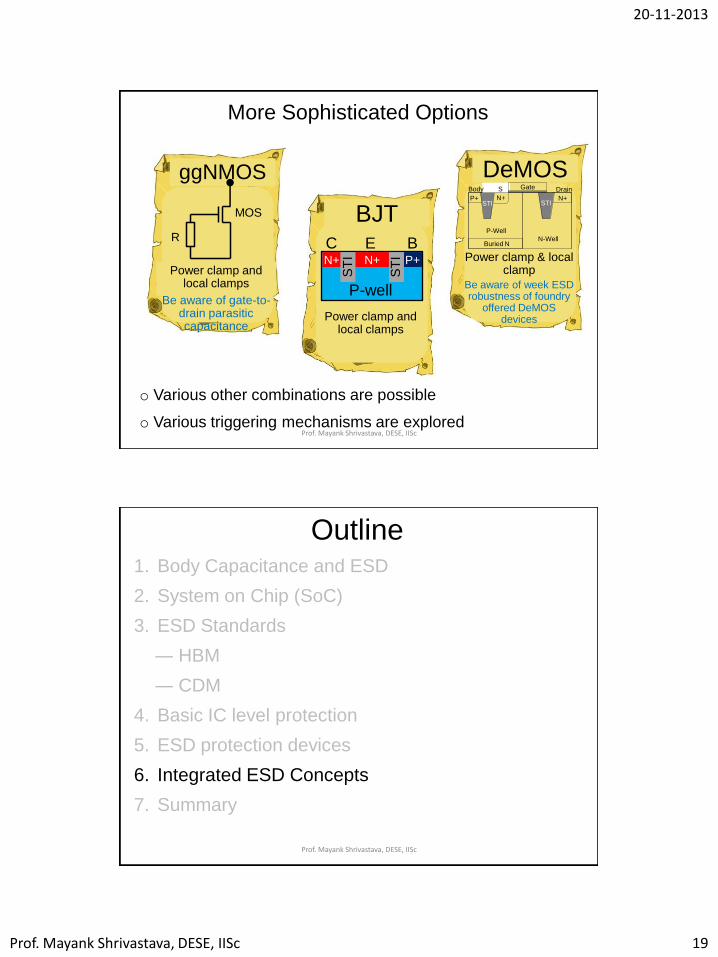
More Sophisticated Options
BJT
Power clamp and local clamps
DeMOS
Power clamp & local clamp
Be aware of week ESD robustness of foundry
offered DeMOS devices
ggNMOS
Power clamp and local clamps
Be aware of gate-to-drain parasitic capacitance
R
MOS
N+P+ N+
Substrate
Gate DrainSBody
Buried N
(a)
FOX FOX
N- - Epi
P- - Body
STI STIN+P+ N+
Substrate
Gate DrainSBody
N-Well
P-Well
Buried N
(c)
N+P+ N+
Substrate
GateSBody
N- - EpiP- - Body
Buried N
(b)
FOX
Drain
STIN+P+ N+
N-Well
P-Well
Substrate
GateSBody Drain
Buried N
(d)
o Various other combinations are possible
o Various triggering mechanisms are explored
N+ P+ N+
P-well
ST
I
ST
I
C E B
Prof. Mayank Shrivastava, DESE, IISc
Outline 1. Body Capacitance and ESD
2. System on Chip (SoC)
3. ESD Standards
― HBM
― CDM
4. Basic IC level protection
5. ESD protection devices
6. Integrated ESD Concepts
7. Summary
Prof. Mayank Shrivastava, DESE, IISc
20-11-2013
Prof. Mayank Shrivastava, DESE, IISc 20
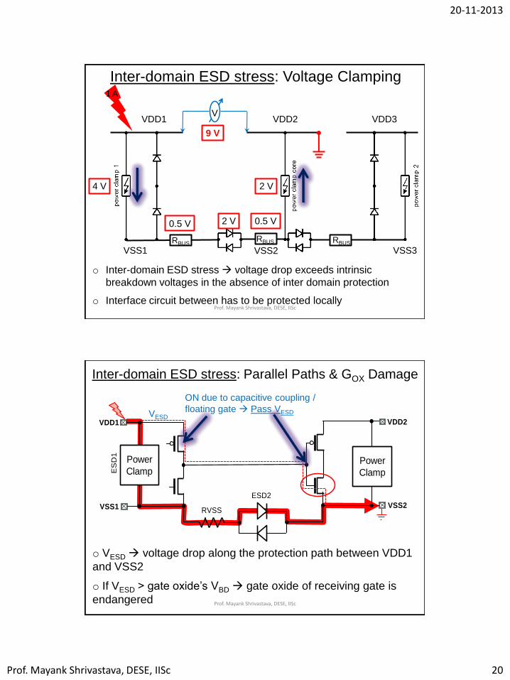
Inter-domain ESD stress: Voltage Clamping
2 V
4 V
0.5 V
VDD1 VDD2 VDD3
0.5 V
2 V
V
9 V
o Inter-domain ESD stress voltage drop exceeds intrinsic
breakdown voltages in the absence of inter domain protection
o Interface circuit between has to be protected locally
VSS1 VSS2 VSS3
1 A
RBUS RBUS RBUS
Prof. Mayank Shrivastava, DESE, IISc
VSS1
VDD1
Power
Clamp
VSS2
VDD2
Power
ClampES
D1
ESD2
RVSS
Inter-domain ESD stress: Parallel Paths & GOX Damage
o VESD voltage drop along the protection path between VDD1
and VSS2
o If VESD > gate oxide’s VBD gate oxide of receiving gate is
endangered
ON due to capacitive coupling /
floating gate Pass VESD VESD
Prof. Mayank Shrivastava, DESE, IISc

20-11-2013
Prof. Mayank Shrivastava, DESE, IISc 21
VSS1
VDD1
Power
Clamp
VSS2
VDD2
Power
ClampES
D1
ESD2
RVSS
Inter-domain ESD stress: Parallel Paths & GOX Damage
VESD
VESD
1K
ESD rules:
― Add voltage clamping elements to gate node
― No thin GOX buffer cap! Prof. Mayank Shrivastava, DESE, IISc
o ESD rule: (N)-diffusions,
which are connected to
different supplies, need
enlarged spacing
o ESD rule: (N)-wells, which
are connected to different
supplies, need enlarged
spacing
VDD1 VDD2
N-well N-well
P-substrate
N+ N+
Larger
spacing
Inter-domain ESD stress: Breakdown Between
Neighbored Diffusions
Prof. Mayank Shrivastava, DESE, IISc

20-11-2013
Prof. Mayank Shrivastava, DESE, IISc 22
4 V
0.5V
VDD1 VDD2 VDD3
4.5V
o Voltage drop might exceed intrinsic breakdown
voltages of sensitive topologies like:
― thin GOX buffer caps
― small LG, thin GOX MOS w/o SBLK
o Such sensitive topologies are forbidden
VSS1
VSS2
VSS3
1 A
V
RBUS RBUS RBUS
Intra-domain ESD stress: Voltage Clamping
Voltage C
urr
ent
1A
4V
Power Clamp Char.
Prof. Mayank Shrivastava, DESE, IISc
2 V
0.5V
VDD1 VDD2 VDD3
2.5V
VSS1
VSS2
VSS3
1 A
V
RBUS RBUS RBUS
Intra-domain ESD stress: Voltage Clamping
o Aggressive voltage clamping e.g. by large
RCMOS power clamp
o Compromises in leakage and area critical
for designs with large number of small power
domains Voltage
Curr
ent
1A
2V 4V
Power Clamp Char.
Prof. Mayank Shrivastava, DESE, IISc

20-11-2013
Prof. Mayank Shrivastava, DESE, IISc 23
o Large PMOS of internal buffer
can deliver high saturation
current (gate is floating)
o Value of current can be high
enough to trigger one finger of
the NMOS
o Unprotected diffusion of
NMOS will be destroyed
Intra-domain ESD stress: Parallel Paths & Large Buffers
ESD rule: Limit ratio of PMOS width (WP1) and smallest NMOS finger width (WN1)
P1
N1 N2 N3 Nn
𝑊𝑃1
𝑊𝑁1< 𝜔; 𝜔 𝑖𝑠 𝑚𝑎𝑥. 𝑟𝑎𝑡𝑖𝑜 𝑎𝑙𝑙𝑜𝑤𝑒𝑑 𝑎𝑛𝑑 𝑁1 𝑖𝑠 𝑡ℎ𝑒 𝑠𝑚𝑎𝑙𝑙𝑒𝑠𝑡 𝑁𝑀𝑂𝑆
ES
D p
ath
Pa
rasitic
E
SD
pa
th
Prof. Mayank Shrivastava, DESE, IISc
Protection Path between Power Rails
o Preferred On-chip metal
shorting of buses with same
potential
o Adequate ESD clamping
between buses at different
potentials
o Different VSS buses requiring
ground separation anti-
parallel diodes
o Double bonding Zener diodes are shown
for simplicity!
Supply domains have to be connected as:
Prof. Mayank Shrivastava, DESE, IISc

20-11-2013
Prof. Mayank Shrivastava, DESE, IISc 24
Package Level Protection Measures
o ESD master bus and
bonding influence the
voltage drop in ESD
discharge path
o The maximum
resistance of the
network is strongly
restricted demands
detailed extraction
Common power ground bar
inside package
1 2 3 4 5 6 7 8 9 10 11
12
13
14
15
16
17
18
19
20
21
22
24 23 26 25 28 27 30 29 32 31 33
44
43
42
41
40
39
38
37
36
35
34
OU
T_1
IN_1
VS
SB
VS
SP
VD
DP
_D
IG1
SPACER
VSSB
VSSP_DIG2
VDDP_DIG2
COMM1
OUT_2
SP
AC
ER
SPACER
OU
T_3
OU
T_4
OU
T_5
VD
D_M
AIN
VS
S
SP
AC
ER
IN_4
IN_5
IN_6
VS
S
VD
D_M
AIN
Prof. Mayank Shrivastava, DESE, IISc
System in Package
Establish ESD protection path between ICs, e.g. by double bonds
Common power ground bar
inside package
OU
T_1
IN_1
VS
SB
VS
SP
VD
DP
_D
IG1
SPACER
VSSB
VSSP_DIG2
VDDP_DIG2
COMM1
OUT_2
SPACER
OU
T_3
OU
T_4
OU
T_5
VD
D_M
AIN
VS
S
SP
AC
ER
IN_4
IN_5
IN_6
VS
S
VD
D_M
AIN
OU
T_1
IN_1
VS
SB
VS
SP
VD
DP
_D
IG1
SPACER
VSSB
VSSP_DIG2
VDDP_DIG2
COMM1
OUT_2
SPACER
OU
T_3
OU
T_4
OU
T_5
VD
D_M
AIN
VS
S
IN_4
IN_5
IN_6
VS
S
VD
D_M
AIN
SP
AC
ER
Prof. Mayank Shrivastava, DESE, IISc

20-11-2013
Prof. Mayank Shrivastava, DESE, IISc 25
System in Package: 3D IC ESD Challenges
Establish ESD protection path beteen ICs, e.g. by double bonds PCB
BGA Laminate
Die-1
TSV
Microbump
Underfill
Package balls
Die-2
Die-3
Die-4
o ESD master bus Dies containing IOs connected to balls need common
ESD master bus
o IO protection:
― IOs connected to balls need to have full ESD protection circuit
― Inputs not connected to balls fine with reduced ESD protection
o Be aware ESD compliance of dies from different suppliers Prof. Mayank Shrivastava, DESE, IISc
Outline 1. Body Capacitance and ESD
2. System on Chip (SoC)
3. ESD Standards
― HBM
― CDM
4. Basic IC level protection
5. ESD protection devices
6. Integrated ESD Concepts
7. Summary
Prof. Mayank Shrivastava, DESE, IISc

20-11-2013
Prof. Mayank Shrivastava, DESE, IISc 26
Summary o Appropriate ESD targets for ICs:
― HBM: 1 KV
― CDM: 250 V
o Scaling of technology narrows window for CDM further!
o Efficient voltage clamping is essential for ESD protection
― Rail based ( dual diode + RCMOS power clamp)
― Local clamp (e.g. SCR) concepts are used
o ESD rules have to be applied for protected circuitry. Most familiar
rules are:
― Cross domain rules
― Restricted use of low voltage devices
o Package design is an integral measure of ESD protection
concepts
― An ESD master bus has to be guaranteed Prof. Mayank Shrivastava, DESE, IISc
ESD in Nanoelectronics
o ESD in Nanoelectronics will be a challenge as new
structures and materials are introduced
o ESD protection of future Nanoelectronic devices
and products will be a challenge due to physical
size, geometries, and performance objectives
Prof. Mayank Shrivastava, DESE, IISc
20-11-2013
Prof. Mayank Shrivastava, DESE, IISc 27
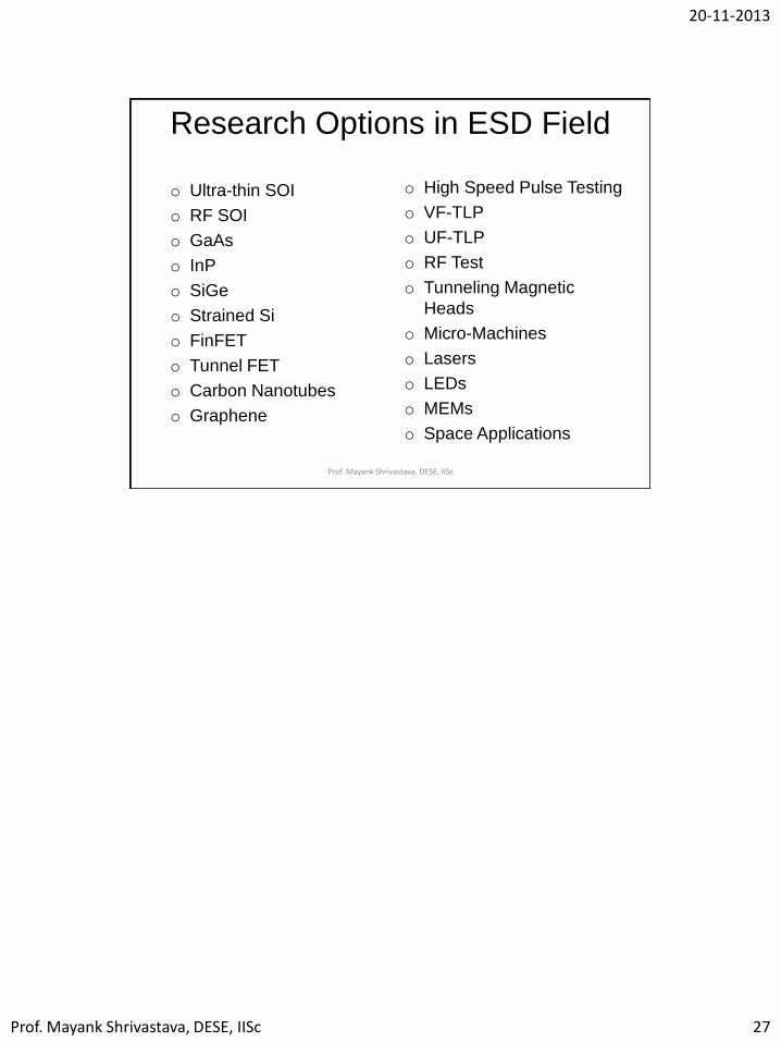
Research Options in ESD Field
o Ultra-thin SOI
o RF SOI
o GaAs
o InP
o SiGe
o Strained Si
o FinFET
o Tunnel FET
o Carbon Nanotubes
o Graphene
o High Speed Pulse Testing
o VF-TLP
o UF-TLP
o RF Test
o Tunneling Magnetic
Heads
o Micro-Machines
o Lasers
o LEDs
o MEMs
o Space Applications
Prof. Mayank Shrivastava, DESE, IISc