avt-822 hardware description description hardware revision “a3” 24 april 2018 avt-84x multiple...
TRANSCRIPT

1509 Manor View Road, Davidsonville, MD 21035 USA +1-410-798-4038 (voice) [email protected]
www.AVT-HQ.com
ADVANCED VEHICLE TECHNOLOGIES, Inc.
AVT – 822
CAN (J1939) and J1708
Controller Board
Hardware Description
Hardware revision “A3” 24 April 2018

AVT-84x Multiple Interface
Advanced Vehicle Technologies, Inc. Page 2
Table of Contents
1. INTRODUCTION ....................................................................................................................................................4
2. GLOSSARY ..............................................................................................................................................................4
2.1 CONVENTIONS.........................................................................................................................................................4
3. BRIEF HISTORY.....................................................................................................................................................4
4. SOFTWARE / FIRMWARE DEVELOPMENT ...................................................................................................5
4.1 FIRMWARE SOURCE CODE ......................................................................................................................................5 4.1.1 Development Environment.................................................................................................................................5 4.1.2 PE Micro............................................................................................................................................................5 4.1.3 Firmware Limitation..........................................................................................................................................5
5. HARDWARE PHYSICAL DESCRIPTION ..........................................................................................................5
5.1 HARDWARE REVISION .............................................................................................................................................5 5.2 BOARD DIMENSIONS ...............................................................................................................................................5 5.3 BOARD TOP IMAGE .................................................................................................................................................6 5.4 CONNECTORS ..........................................................................................................................................................6 5.5 PHOTO.....................................................................................................................................................................6
6. CIRCUIT DESIGN DESCRIPTION ......................................................................................................................7
6.1 SCHEMATIC .............................................................................................................................................................7 6.2 MICROCONTROLLER................................................................................................................................................7
6.2.1 CAN Channel 0 ..................................................................................................................................................8 6.2.2 CAN Channel 4 ..................................................................................................................................................8 6.2.3 SPI channel 0.....................................................................................................................................................8 6.2.4 SPI Channel 1 ....................................................................................................................................................8 6.2.5 BDM...................................................................................................................................................................8 6.2.6 Heartbeat Indicator ...........................................................................................................................................8 6.2.7 Unused Ports .....................................................................................................................................................9
6.3 PROGRAMMABLE INTERVAL TIMER ........................................................................................................................9 6.3.1 Timer0................................................................................................................................................................9 6.3.2 Timer1................................................................................................................................................................9 6.3.3 Timer2................................................................................................................................................................9
7. ELECTRICAL CONNECTION DESCRIPTIONS ...............................................................................................9
7.1 P1 – DEBUG ..........................................................................................................................................................10 7.2 P2 – POWER ..........................................................................................................................................................10 7.3 P3 – PGM .............................................................................................................................................................10 7.4 P4 – CAN BUS ......................................................................................................................................................11 7.5 P7 – OUTPUTS .......................................................................................................................................................11 7.6 P6 – INPUTS ..........................................................................................................................................................11 7.7 P5 – J1708 BUS.....................................................................................................................................................12
8. CAN MESSAGES...................................................................................................................................................12
8.1 XXX – REPORTED ..................................................................................................................................................12 8.2 XXX – COMMANDED .............................................................................................................................................12
9. J1708 MESSAGE DESCRIPTIONS.....................................................................................................................12
9.1 XXX – REPORTED ..................................................................................................................................................12 9.2 XXX – COMMANDED .............................................................................................................................................12
10. OPERATIONS ...................................................................................................................................................13

AVT-84x Multiple Interface
Advanced Vehicle Technologies, Inc. Page 3
10.1 START UP..............................................................................................................................................................13 10.2 START UP COMMANDS..........................................................................................................................................13 10.3 CONTROLLER OPERATIONS ...................................................................................................................................13 10.4 OPERATIONAL PARAMETERS .................................................................................................................................13 10.5 HEARTBEAT INDICATOR ........................................................................................................................................13
11. PASSIVE OPERATIONS..................................................................................................................................13
11.1 XXX.......................................................................................................................................................................13
12. ACTIVE OPERATIONS ...................................................................................................................................13
12.1 XXX.......................................................................................................................................................................13
13. DEBUG PORT....................................................................................................................................................13
13.1 CONNECTION TO A COMPUTER ..............................................................................................................................13 13.2 BAUD RATE...........................................................................................................................................................15
14. IDLE MODE - COMMANDS...........................................................................................................................16
15. CAN MODE - COMMANDS............................................................................................................................17
16. J1708 – COMMANDS .......................................................................................................................................18
17. QUESTIONS ??..................................................................................................................................................19

AVT-84x Multiple Interface
Advanced Vehicle Technologies, Inc. Page 4
1. Introduction
This document describes the AVT-822 hardware.
Electrical and physical information about the AVT-822 board is provided.
Some (limited) discussion of firmware is also provided.
2. Glossary
Common terms, abbreviations, acronyms, and more.
$ Dollar sign: indicates a hex number.
CAN Controller Area Network
CAN0 CAN channel 0
CAN4 CAN channel 4
EEPROM Electrically Erasable Programmable Read Only Memory. Usually with the form of small rows and sectors. Erase and program operations are usually done for one sector at a time.
FLASH A form of EEPROM. Usually with the form of large rows and sectors. Erase and program operations are usually done for one sector at a time.
J1708 SAE specification for a (relatively) low speed, two-wire, multi-drop network. The signaling is UART based.
ISO 11898 ISO specification for 2-wire CAN physical layer.
J1939 SAE specification for messages on a 2-wire CAN network. A very detailed specification covering a very wide range of information.
msec. Millisecond, 1/1000 of a second.
2.1 Conventions
I try to follow these rules and conventions.
NOTE: I try to prefix all HEX numbers with the “$” sign. All other numbers are decimal. If you have a question about any numbers, ask me.
NOTE: In keeping with the SAE J1939 documentation … Bytes in a CAN frame are numbered 1 to 8. Bits are numbered 1 to 8.
3. Brief History
AVT-84x Multiple Interface
Advanced Vehicle Technologies, Inc. Page 5
4. Software / Firmware Development
The AVT-822 is being sold as a hardware platform.
It is expected that the user will want to develop their own software / firmware to meet their specific needs.
4.1 Firmware Source Code
AVT may be able to supply some firmware source code to help the user get up and running.
4.1.1 Development Environment
All AVT developed firmware was written in HCS12 assembly language.
The PE Micro HCS12 assembler and ‘logical to physical’ converter applications were used to generate the final S19 file.
The PE Micro USB Multilink in-circuit programmer (and debugger) was used to program the FLASH memory on the microcontroller.
4.1.2 PE Micro
Information about all PE Micro products for the HCS12 family can be found at the PE Micro web site:
http://www.pemicro.com/index.cfm
4.1.3 Firmware Limitation
At present, there is no J1708 support in the firmware. Activity on the J1708 port is ignored.
5. Hardware Physical Description
In this section I describe the board hardware.
The inputs and outputs are described generically since it is up to the user to define their use.
Consult the original AVT-822 ICD (Interface Control Document) for a complete description of all inputs and outputs as used with the original production firmware.
5.1 Hardware Revision
The AVT-822 board revision stands at “A3” – Production.
Refer to our web site for the most up-to-date information about the hardware status of this board.
Hardware status: www.AVT-HQ.com/822_hw.htm
5.2 Board Dimensions
The board outline is: 3.0 x 4.0 inches.

AVT-84x Multiple Interface
Advanced Vehicle Technologies, Inc. Page 6
Maximum height is 0.5 inches. This is due to the pin headers at P1 (debug) and P3 (programming). P1 can be removed. P3 is only needed to initially program the microcontroller. If P1 and P3 are removed, the board maximum height is 0.3 inches.
5.3 Board Top Image
Shown below is a plot of the top of the board showing all component locations and designations.
Connector locations and designations are shown as well.
5.4 Connectors
The connector outlines shown at P2, P4 P5, P6 and P7 are not installed.
5.5 Photo
Here is a photo of a production board.

AVT-84x Multiple Interface
Advanced Vehicle Technologies, Inc. Page 7
6. Circuit Design Description
6.1 Schematic
The board schematic may be available, on request.
6.2 Microcontroller
A Motorola / Freescale / NXP microcontroller of the HCS12 family is used on the AVT-822 and designated U1.
The part number is: MC9S12DG128CPVE.
This microcontroller contains the following:
• 128 K bytes of FLASH non-volatile memory.
• 2 K bytes of EEPROM non-volatile memory.
• 8 K bytes of RAM.
• Two CAN controllers of the MSCAN family.

AVT-84x Multiple Interface
Advanced Vehicle Technologies, Inc. Page 8
• Two UART serial ports.
The microcontroller uses an external 8.0000 MHz ceramic resonator for the internal PLL reference.
All documentation for the microcontroller can be obtained directly from the NXP website. I can provide some Freescale documents, by email, on request.
6.2.1 CAN Channel 0
Microcontroller CAN channel 0 is connected to P4.
An NXP TJA1050T transceiver is used to provide an ISO 11898-2 compliant CAN bus connection.
CAN bus termination components are designed onto the AVT-822 board, but they are not installed. A split termination design is used. Component specifications can be provided on request.
6.2.2 CAN Channel 4
Microcontroller CAN channel 4 is not used.
The microcontroller pins for CAN channel 4 are routed to empty pads on the board. They are available for future use. No space or pads are allocated for a transceiver.
6.2.3 SPI channel 0
Microcontroller Serial Peripheral Interface (SPI) channel 0 is connected to P1.
This connection was intended to be a debug connection. But it can be used as desired.
A separate (small) communications adapter board can be connected to P1. The small adapter board provides an RS-232 communications port to an external computer.
6.2.4 SPI Channel 1
Microcontroller Serial Peripheral Interface (SPI) channel 1 is connected to P5.
A Exar SP485EMN-L transceiver is used to provide an SAE J1708 compliant connection.
The AVT-822 implements the J1708 transceiver and termination as described in SAE specification J1708 rev. OCT93.
6.2.5 BDM
Microcontroller Background Debug Monitor (BDM) port is connected to P3.
This is only used for programming the microcontroller and, if enabled, for debug monitoring of the microcontroller internal operations. I used the PE Micro USB Multilink in-circuit programmer (and debugger) to connect to P3 for programming and (when enabled) internal microcontroller operations.
Otherwise, nothing should ever be connected to P3.
6.2.6 Heartbeat Indicator
Microcontroller port A0 is connected to the anode of a small red LED on the AVT-822 board.
The red LED cathode is connected to ground. A high on Port A0 will turn the red LED on.

AVT-84x Multiple Interface
Advanced Vehicle Technologies, Inc. Page 9
Microcontroller firmware is usually written to blink the LED to provide a visual indication that the microcontroller is “alive” and running.
6.2.7 Unused Ports
All other microcontroller ports and pins are routed to empty pads on the board for easy access for future use.
6.3 Programmable Interval Timer
Included on the board is an Intersil CS82C54Z Programmable Interval Timer. The CS82C54Z device includes three 16-bit timers; each timer is independent.
The CS82C54Z is controlled by the microcontroller. The connections are listed here.
Microcontroller port B0 thru B7 are connected to the data pins D0 thru D7.
Microcontroller port K0 is connected to address pin A0.
Microcontroller port K1 is connected to address pin A1.
Microcontroller port K2 is connected to the NOT CHIP SELECT pin.
Microcontroller port K3 is connected to the NOT READ pin.
Microcontroller port K4 is connected to the NOT WRITE pin.
Microcontroller port M5 is connected to Gate0 pin.
Microcontroller port M6 is connected to Gate1 pin.
Microcontroller port M7 is connected to Gate2 pin.
6.3.1 Timer0
The clock source for Timer0 is microcontroller port P5, which is PWM5. Microcontroller PWM5 is set up as a variable frequency clock generator.
The output of Timer0 is routed through a 74HC126 buffer to P7 pin # 1.
6.3.2 Timer1
The clock source for Timer1 is microcontroller port P6, which is PWM6. Microcontroller PWM6 is set up as a variable frequency clock generator.
The output of Timer1 is routed through a 74HC126 buffer to P7 pin # 2.
6.3.3 Timer2
The clock source for Timer2 is microcontroller port P7, which is PWM7. Microcontroller PWM7 is set up as a variable frequency clock generator.
The output of Timer2 is routed to an empty pad on the board. It is available for a future use.
7. Electrical Connection Descriptions
All electrical connections to the AVT-822 board are described here.

AVT-84x Multiple Interface
Advanced Vehicle Technologies, Inc. Page 10
No connectors are installed for P2, P4, P6 and P7. There are two (2) thru-hole solder connections on the board for each signal described.
7.1 P1 – Debug
This is a connection to the microcontroller Serial Peripheral Interface (SPI) channel 0.
Square pad indicates pin #1.
Pin # 1: VCC (+5 vdc).
Pin # 2: Ground.
Pin # 3: TXD (out); microcontroller port S1, SPI0, TXD0.
Pin # 4: RXD (in); microcontroller port S0 SPI0, RXD0.
Pin # 5: RTS (out); microcontroller port A1.
Pin # 6: CTS (in) ; microcontroller port A2.
A separate communications adapter board can be connected to P1 which will then provide an RS-232 communications port to an external computer for debug and operational monitoring purposes. Refer to Section 13 for details about the debug port and adapter.
7.2 P2 – Power
Square pad indicates pin #1.
Pin # 1: +8 to +36 VDC ~ 60 milliamps
Pin # 2: Ground (or supply return).
Pin # 1 is routed through a TE Connectivity ASMD030-F2 resettable fuse. That is followed by an SS14 reverse polarity protection diode.
On-board +5 VDC (VCC) power is the provided by an On-Semi MC7805ABD2TG fixed voltage regulator mounted to a big foil heat sink.
7.3 P3 – PGM
This is a connection to the microcontroller Background Debug Monitor (BDM) port.
Square pad indicates pin #1.
Pin # 1: Microcontroller signal BKGD with passive 10 K ohm pull-up to VCC (+5 vdc).
Pin # 2: Ground.
Pin # 3: No connection.
Pin # 4: Microcontroller signal RESET.
Pin # 5: No connection.
Pin # 6: No connection.

AVT-84x Multiple Interface
Advanced Vehicle Technologies, Inc. Page 11
7.4 P4 – CAN bus
This is a connection to the microcontroller CAN channel 0.
Square pad indicates pin #1.
Pin # 1: CAN_H signal.
Pin # 2: ground
Pin # 3: CAN_L signal.
7.5 P7 – Outputs
Square pad indicates pin #1.
Pin # 1: signal name: CS82C54Z Timer0. type: Output (through 74HC126 buffer). description: +5 V HCMOS compatible
Pin # 2: signal name: CS82C54Z Timer1. type: Output (through 74HC126 buffer). description: +5 V HCMOS compatible
Pin # 3: signal name: Microcontroller port M2. type: Output (through 74HC126 buffer). description: +5 V HCMOS compatible.
Pin # 4: signal name: Microcontroller port M3. type: Output (through 74HC126 buffer). description: +5 V HCMOS compatible.
Pin # 5: signal name: GROUND type: Reference ground for signals on pins 1 through 4.
7.6 P6 – Inputs
Square pad indicates pin #1.
Pin # 1: signal name: Microcontroller port A3. type: Input (through 74HC14 Schmitt trigger buffer). +5 V HCMOS compatible. Passively pulled high through 10 Kohm resistor.
Pin # 2: signal name: Microcontroller port A4. type: Input (through 74HC14 Schmitt trigger buffer). +5 V HCMOS compatible. Passively pulled high through 10 Kohm resistor.
AVT-84x Multiple Interface
Advanced Vehicle Technologies, Inc. Page 12
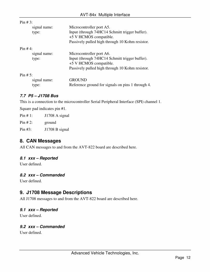
Pin # 3: signal name: Microcontroller port A5. type: Input (through 74HC14 Schmitt trigger buffer). +5 V HCMOS compatible. Passively pulled high through 10 Kohm resistor.
Pin # 4: signal name: Microcontroller port A6. type: Input (through 74HC14 Schmitt trigger buffer). +5 V HCMOS compatible. Passively pulled high through 10 Kohm resistor.
Pin # 5: signal name: GROUND type: Reference ground for signals on pins 1 through 4.
7.7 P5 – J1708 Bus
This is a connection to the microcontroller Serial Peripheral Interface (SPI) channel 1.
Square pad indicates pin #1.
Pin # 1: J1708 A signal
Pin # 2: ground
Pin #3: J1708 B signal
8. CAN Messages
All CAN messages to and from the AVT-822 board are described here.
8.1 xxx – Reported
User defined.
8.2 xxx – Commanded
User defined.
9. J1708 Message Descriptions
All J1708 messages to and from the AVT-822 board are described here.
9.1 xxx – Reported
User defined.
9.2 xxx – Commanded
User defined.

AVT-84x Multiple Interface
Advanced Vehicle Technologies, Inc. Page 13
10. Operations
The AVT-822 does not have a power switch. The controller powers up and begins operations as soon as power is applied.
10.1 Start Up
User defined.
10.2 Start Up Commands
None at this time. User defined.
10.3 Controller Operations
User defined.
10.4 Operational Parameters
User defined.
10.5 Heartbeat Indicator
A red LED on the board is controlled by the microcontroller.
11. Passive Operations
User defined.
11.1 xxx
User defined.
12. Active Operations
User defined.
12.1 xxx
User defined.
13. Debug Port
Connector P1 on the AVT-822 provides for a possible RS-232 serial communications connection to an external test computer for debug, monitor, or whatever function(s) the user so desires.
User designed firmware must support this function.
13.1 Connection to a Computer
A special adapter is required.
I ‘might’ be able to supply one, on request and if available.
AVT-84x Multiple Interface
Advanced Vehicle Technologies, Inc. Page 14
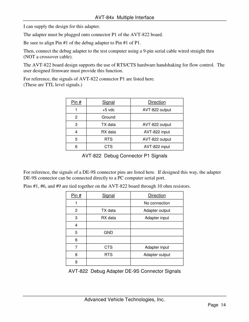
I can supply the design for this adapter.
The adapter must be plugged onto connector P1 of the AVT-822 board.
Be sure to align Pin #1 of the debug adapter to Pin #1 of P1.
Then, connect the debug adapter to the test computer using a 9-pin serial cable wired straight thru (NOT a crossover cable).
The AVT-822 board design supports the use of RTS/CTS hardware handshaking for flow control. The user designed firmware must provide this function.
For reference, the signals of AVT-822 connector P1 are listed here. (These are TTL level signals.)
Pin # Signal Direction
1 +5 vdc AVT-822 output
2 Ground
3 TX data AVT-822 output
4 RX data AVT-822 input
5 RTS AVT-822 output
6 CTS AVT-822 input
AVT-822 Debug Connector P1 Signals
For reference, the signals of a DE-9S connector pins are listed here. If designed this way, the adapter DE-9S connector can be connected directly to a PC computer serial port.
Pins #1, #6, and #9 are tied together on the AVT-822 board through 10 ohm resistors.
Pin # Signal Direction
1 No connection
2 TX data Adapter output
3 RX data Adapter input
4
5 GND
6
7 CTS Adapter input
8 RTS Adapter output
9
AVT-822 Debug Adapter DE-9S Connector Signals

AVT-84x Multiple Interface
Advanced Vehicle Technologies, Inc. Page 15
13.2 Baud Rate
The serial communications baud rate between the AVT-822 and the test computer is specified by the user designed firmware.

AVT-84x Multiple Interface Idle mode
Advanced Vehicle Technologies, Inc. Page 16
14. Idle Mode - Commands
All commands and responses are user defined.

AVT-822 Controller CAN Operations
Advanced Vehicle Technologies, Inc. Page 17
15. CAN Mode - Commands
All commands and responses are user defined.
AVT-822 Controller J1708 Operations
Advanced Vehicle Technologies, Inc. Page 18
16. J1708 – Commands
All commands and responses are user defined.
AVT-84x Multiple Interface Appendix A
Advanced Vehicle Technologies, Inc. Page 19
17. Questions ??
Contact the factory by e-mail, phone, or fax. Contact information is provided here and on the bottom of page 1.
Post: 1509 Manor View Road
Davidsonville, MD 21035 USA
Phone: +1-410-798-4038
E-mail: [email protected]
Web site: http://www.AVT-HQ.com/