av02-0235en ds acsl-6xx0 05feb2010
TRANSCRIPT
ACSL-6xx0 Multi-Channel and Bi-Directional,
15 MBd Digital Logic Gate Optocoupler
Data Sheet
Description
ACSL-6xx0 are truly isolated, multi-channel and bi-direc-tional, high-speed optocouplers. Integration of multiple optocouplers in monolithic form is achieved through patented process technology. These devices provide full duplex and bi-directional isolated data transfer and communication capability in compact surface mount packages. Available in 15 Mbd speed option and wide supply voltage range.
These high channel density make them ideally suited to isolating data conversion devices, parallel buses and peripheral interfaces.
They are available in 8-pin and 16–pin narrow-body SOIC package and are specified over the temperature range of -40°C to +100°C.
Features
� Available in dual, triple and quad channel configura-tions
� Bi-directional
� Wide supply voltage range: 3.0V to 5.5V
� High-speed: 15 MBd typical, 10 MBd minimum
� 10 kV/μs minimum Common Mode Rejection (CMR) at Vcm = 1000V
� LSTTL/TTL compatible
� Safety and regulatory approvals– 2500Vrms for 1 min per UL1577 – CSA Component Acceptance – IEC/EN/DIN EN 60747-5-2
� 16 Pin narrow-body SOIC package for triple and quad channel
� -40 to 100°C temperature range
Applications
� Serial Peripheral Interface (SPI)
� Inter-Integrated Interface (I2C)
� Full duplex communication
� Isolated line receiver
� Microprocessor system interfaces
� Digital isolation for A/D and D/A conversion
� Instrument input/output isolation
� Ground loop elimination
CAUTION: It is advised that normal static precautions be taken in handling and assemblyof this component to prevent damage and/or degradation, which may be induced by ESD.
Lead (Pb) FreeRoHS 6 fullycompliant
RoHS 6 fully compliant options available;-xxxE denotes a lead-free product
2
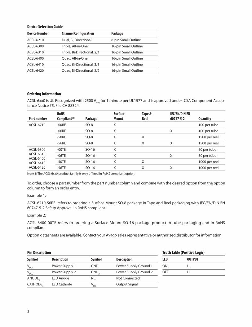
Device Selection Guide
Device Number Channel Configuration Package
ACSL-6210 Dual, Bi-Directional` 8-pin Small Outline
ACSL-6300 Triple, All-in-One 16-pin Small Outline
ACSL-6310 Triple, Bi-Directional, 2/1 16-pin Small Outline
ACSL-6400 Quad, All-in-One 16-pin Small Outline
ACSL-6410 Quad, Bi-Directional, 3/1 16-pin Small Outline
ACSL-6420 Quad, Bi-Directional, 2/2 16-pin Small Outline
Pin Description
Symbol Description Symbol Description
VDD1
Power Supply 1 GND1 Power Supply Ground 1
VDD2
Power Supply 2 GND2 Power Supply Ground 2
ANODEx LED Anode NC Not Connected
CATHODEx LED Cathode V
OX Output Signal
Truth Table (Positive Logic)
LED OUTPUT
ON L
OFF H
Ordering Information
ACSL-6xx0 is UL Recognized with 2500 Vrms
for 1 minute per UL1577 and is approved under CSA Component Accep-tance Notice #5, File CA 88324.
Part number
RoHS
Compliant [1] Package
Surface
Mount
Tape &
Reel
IEC/EN/DIN EN
60747-5-2 Quantity
ACSL-6210 -00RE SO-8 X 100 per tube
-06RE SO-8 X X 100 per tube
-50RE SO-8 X X 1500 per reel
-56RE SO-8 X X X 1500 per reel
ACSL-6300ACSL-6310ACSL-6400ACSL-6410ACSL-6420
-00TE SO-16 X 50 per tube
-06TE SO-16 X X 50 per tube
-50TE SO-16 X X 1000 per reel
-56TE SO-16 X X X 1000 per reel
Note 1: The ACSL-6xx0 product family is only offered in RoHS compliant option.
To order, choose a part number from the part number column and combine with the desired option from the option column to form an order entry.
Example 1:
ACSL-6210-56RE refers to ordering a Surface Mount SO-8 package in Tape and Reel packaging with IEC/EN/DIN EN 60747-5-2 Safety Approval in RoHS compliant.
Example 2:
ACSL-6400-00TE refers to ordering a Surface Mount SO-16 package product in tube packaging and in RoHS compliant.
Option datasheets are available. Contact your Avago sales representative or authorized distributor for information.
3
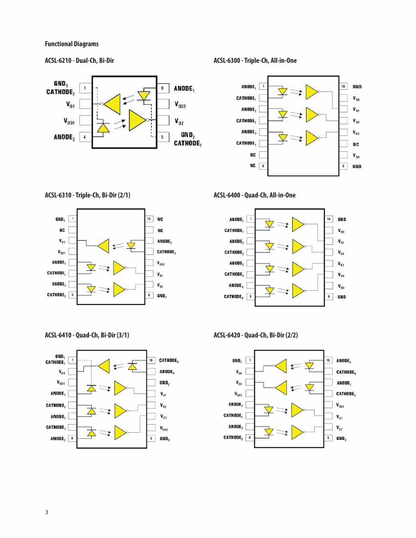
Functional Diagrams
ACSL-6210 - Dual-Ch, Bi-Dir ACSL-6300 - Triple-Ch, All-in-One
ACSL-6310 - Triple-Ch, Bi-Dir (2/1) ACSL-6400 - Quad-Ch, All-in-One
ACSL-6410 - Quad-Ch, Bi-Dir (3/1) ACSL-6420 - Quad-Ch, Bi-Dir (2/2)
4
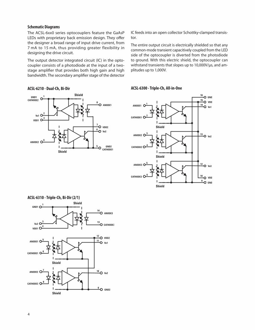
Schematic Diagrams
ACSL-6210 - Dual-Ch, Bi-Dir ACSL-6300 - Triple-Ch, All-in-One
ACSL-6310 - Triple-Ch, Bi-Dir (2/1)
Shield
GND2CATHODE1
4
5
6
7VDD2
ANODE2
Vo2
Shield1
2
ANODE1
3
8
GND1CATHODE2
VDD1
Vo1
16
Shield
1
2
15
14ANODE1
CATHODE1
VDD
GND
Vo1
Shield
3
4
13
CATHODE2
ANODE2 Vo2
Shield
5
6
12
10
9
CATHODE3
ANODE3
VDD
GND
Vo3
Shield1
3
ANODE3
4
14
GND1
VDD1
Vo3 CATHODE313
Shield
5
6
12
11ANODE1
CATHODE1
VDD2
Vo1
Shield
7
8
10
9
CATHODE2
ANODE2
GND2
Vo2
The ACSL-6xx0 series optocouplers feature the GaAsP LEDs with proprietary back emission design. They offer the designer a broad range of input drive current, from 7 mA to 15 mA, thus providing greater flexibility in designing the drive circuit.
The output detector integrated circuit (IC) in the opto-coupler consists of a photodiode at the input of a two-stage amplifier that provides both high gain and high bandwidth. The secondary amplifier stage of the detector
IC feeds into an open collector Schottky-clamped transis-tor.
The entire output circuit is electrically shielded so that any common-mode transient capacitively coupled from the LED side of the optocoupler is diverted from the photodiode to ground. With this electric shield, the optocoupler can withstand transients that slopes up to 10,000V/μs, and am-plitudes up to 1,000V.

5
ACSL-6410 - Quad-Ch, Bi-Dir (3/1)
ACSL-6420 - Quad-Ch, Bi-Dir (2/2)
Schematic Diagrams, continued
Shield
2
1GND1
Vo4
Shield
4
3
VDD1
Vo3
14
13
ANODE3
CATHODE3
16
15
ANODE4
CATHODE4
Shield
5
6
12
11ANODE1
CATHODE1
VDD2
Vo1
Shield
7
8
10
9
CATHODE2
ANODE2
GND2
Vo2
Shield
13
GND2
Vo1
Shield
12Vo2
Shield
11
10
9VDD2
GND2
Vo3
4ANODE1
6
5
ANODE2
CATHODE2
8
7
ANODE3
CATHODE3
14
Shield1
2
3
GND1CATHODE1
VDD1
Vo4 ANODE415
CATHODE416
Shield
1
2
16
15
14ANODE1
CATHODE1
VDD
GND
Vo1
Shield
3
4
13
CATHODE2
ANODE2 Vo2
Shield
5
6
12
CATHODE3
ANODE3 Vo3
Shield
7
8
11
10
9
CATHODE4
ANODE4
VDD
GND
Vo4
ACSL-6400 - Quad-Ch, All-in-One

6
ACSL-6210 Small Outline SO-8 Package
ACSL-6300, ACSL-6310, ACSL-6400, ACSL-6410
and ACSL-6420 Small Outline SO-16 Package
Package Outline Drawings
8 7 6 5
4321
0.228 (5.80)
0.244 (6.20)
0.189 (4.80)
0.197 (5.00)
0.150 (3.80)
0.157 (4.00)
0.013 (0.33)
0.020 (0.51)
0.040 (1.016)
0.060 (1.524)
0.004 (0.10)
0.010 (0.25)0.054 (1.37)
0.069 (1.75)
0.016 (0.40)
0.050 (1.27)
0.008 (0.19)
0.010 (0.25)
0.010 (0.25)
0.020 (0.50)
x 45°
0°
8 °
DIMENSIONS: INCHES (MILLIMETERS)MIN
MAX
18
0.228 (5.791)
0.244 (6.197)
0.386 (9.802)
0.394 (9.999)
0.152 (3.861)
0.157 (3.988)
0.013 (0.330)
0.020 (0.508)
0.040 (1.016)
0.060 (1.524)
0.050 (1.270)
0.060 (1.524)
0.054 (1.372)
0.068 (1.727)
0.004 (0.102)
0.010 (0.249)
0.016 (0.406)
0.050 (1.270)
0.010 (0.245)
0.020 (0.508)0.008 (0.191)
0.010 (0.249)
x 45°
0 - 8° TYP.
DIMENSIONS: INCHES (MILLIMETERS)MIN
MAX

7
Solder Reflow Temperature Profile
Recommended Pb-free IR Profile
Note: Non-halide flux should be used
Note: Non-halide flux should be used
0
TIME (SECONDS)
TEM
PER
ATU
RE
(°C)
200
100
50 150100 200 250
300
0
30SEC.
50 SEC.
30SEC.
160 °C
140 C150 °C°
PEAKTEMP.245 °C
PEAKTEMP.240 °C
PEAKTEMP.230 °C
SOLDERINGTIME
200 °C
PREHEATING TIME150 C, 90 ± 30 SEC.
2.5 °C ± 0.5 °C/SEC.
3 °C + 1 °C/–0.5 °C
TIGHT
TYPICAL
LOOSEROOM
TEMPERATURE
PREHEATING RATE 3°C + 1 °C/–0.5 °C/SEC.
REFLOW HEATING RATE 2.5 °C ± 0.5 °C/SEC.

8
Regulatory Information
Insulation and Safety Related Specifications
Parameter Symbol Value Units Conditions
Minimum External Air Gap L(I01) 4.9 mm Measured from input terminals to output (Clearance) terminals, shortest distance through air
Minimum Externa l Tracking L(I02) 4.5 mm Measured from input terminals to output (Creepage) terminals, shortest distance path through body
Minimum Internal Plastic Gap 0.08 mm Insulation thickness between emitter and (Internal Clearance) detector; also known as distance through insulation
Tracking Resistance CTI 175 Volts DIN IEC 112/VDE0303 Part 1 (Comparative Tracking Index)
Isolation Group IIIa Material Group (DIN VDE 0110, 1/89, Table 1)
IEC/EN/DIN EN 60747-5-2 Insulation Related Characteristics (Option X6X Only)
Description Symbol ACSL-6XX0-X6X Units
Installation Classification per DIN VDE 0110/1.89, Table 1 for rated mains voltage ≤150V rms I-IV for rated mains voltage ≤300V rms I-III
Climatic Classification 55/100/21
Pollution Degree (DIN VDE 0110/1.89) 2
Maximum Working Insulation Voltage VIORM
560 Vpeak
Input to Output Test Voltage, Method b * VPR
1050 Vpeak
VIORM
x 1.875 = VPR
, 100% Production Test with t
m = 1 sec, Partial Discharge < 5 pC
Input to Output Test Voltage, Method a * VPR
840 Vpeak
V
IORM x 1.5 = V
PR, Type and Sample Test,
Tm
= 60 sec, Partial Discharge < 5 pC
Highest Allowable Overvoltage * VIOTM
4000 Vpeak
(Transient Overvoltage, t
ini = 10 sec)
Safety Limiting Values (Maximum values allowed in the event of a failure) Case Temperature T
S 175 °C
Input Current IS,INPUT
150 mA Output Power P
S,OUTPUT 600 mW
Insulation Resistance at TS, V
IO = 500V R
IO 109 Ω
*Refer to the front of the optocoupler section of the current catalog, under Product Safety Regulations section, IEC/EN/DIN EN 60747-5-2, for a detailed description.
Note: Isolation characteristics are guaranteed only within the safety maximum ratings, which must be ensured by protective circuits in applica-tion.
Ts-Case Temperature,°C
Out
put P
ower
-Ps
Inpu
t Pow
er-l
p
700
600
500
400
300
200
100
00 2005025 75 100 125 150 175
Is (mA)Ps (mW)

9
Absolute Maximum Ratings
Parameter Symbol Min. Max. Units
Storage Temperature Ts -55 125 °C
Operating Temperature TA -40 100 °C
Supply Voltage (1 Minute Maximum) VDD1
, VDD2
7 V
Reverse Input Voltage (Per Channel) VR 5 V
Output Voltage (Per Channel) VO 7 V
Average Forward Input Current[1] (Per Channel) IF 15 mA
Output Current (Per Channel) IO 50 mA
Input Power Dissipation[2] (Per Channel) PI 27 mW
Output Power Dissipation[2] (Per Channel) PO 65 mW
Recommended Operating Conditions
Parameter Symbol Min. Max. Units
Operating Temperature TA -40 100 °C
Input Current, Low Level[3] IFL
0 250 μA
Input Current, High Level[4] IFH
7 15 mA
Supply Voltage VDD1
, VDD2
3.0 5.5 V
Fan Out (at RL = 1kΩ) N 5 TTL Loads
Output Pull-up Resistor RL 330 4k Ω
Notes:1. Peaking circuits may produce transient input currents up to 50 mA, 50 ns max. pulse width, provided average current does not exceed its max.
values.2. Derate total package power dissipation, PT linearly above +95°C free-air temperature at a rate of 1.57mW/°C for the SO8 package mounted on
low conductivity board per JESD 51-3. Derate total package power dissipation, PT linearly above +80°C free-air temperature at a rate of 1.59 mW/°C for the SO16 package mounted on low conductivity board per JESD 51-3. PT= number of channels multiplied by (PI+PO).
3. The off condition can be guaranteed by ensuring that VFL
≤ 0.8V.4. The initial switching threshold is 7 mA or less. It is recommended that minimum 8 mA be used for best performance and to permit guardband
for LED degradation.
0
10
20
30
40
50
60
70
80
90
100
0 20 40 60 80 100 120
TA - Ambient Temperature - oC
PT
- To
tal P
ow
er D
issi
pat
ion
per
ch
ann
el -
mW
so-16 package
so-8 package

10
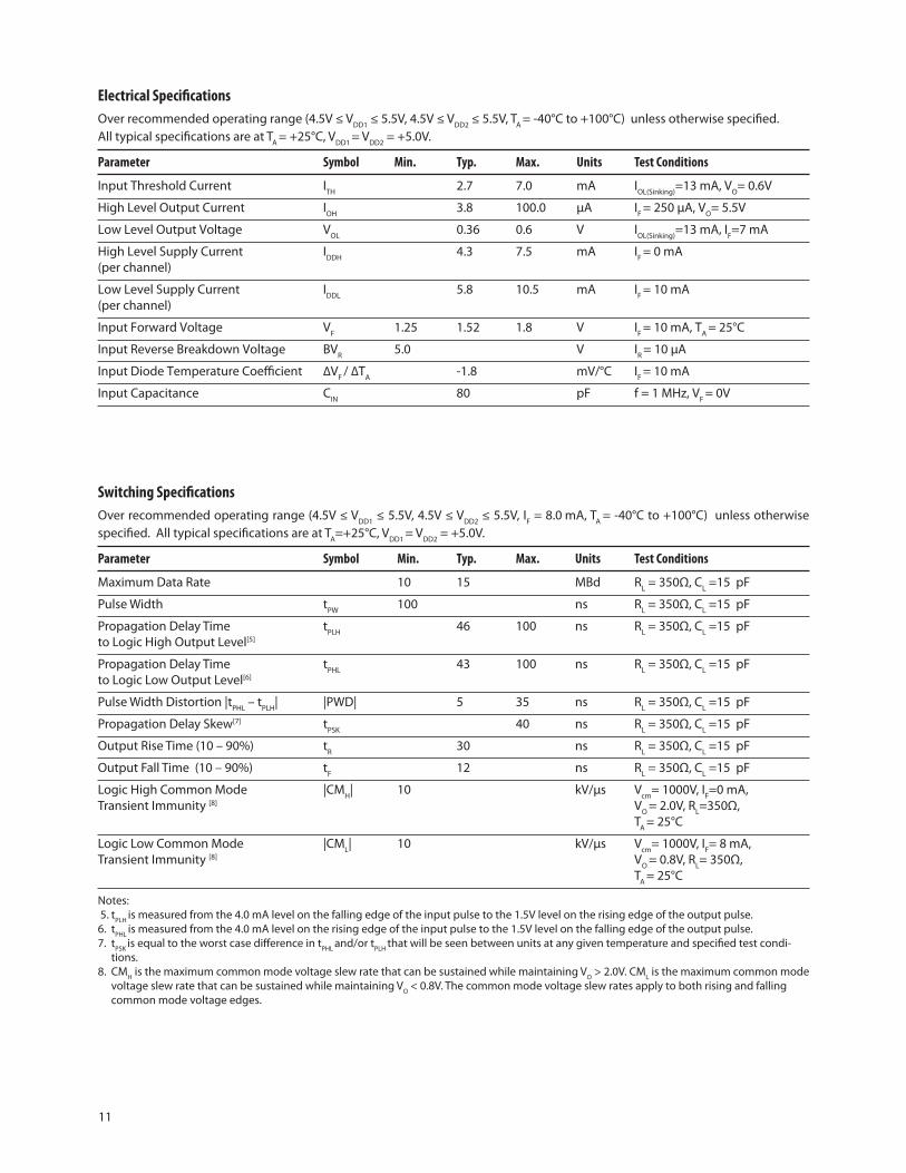
Electrical Specifications
Over recommended operating range (3.0V ≤ VDD1
≤ 3.6V, 3.0V ≤ VDD2
≤ 3.6V, TA
= -40°C to +100°C) unless otherwise specified. All typical specifications are at T
A = +25°C , V
DD1 = V
DD2 = +3.3V.
Parameter Symbol Min. Typ. Max. Units Test Conditions
Input Threshold Current ITH
2.7 7.0 mA IOL(Sinking)
=13 mA, VO
= 0.6V
High Level Output Current IOH
4.7 100.0 μA IF= 250 μA, V
O= 3.3V
Low Level Output Voltage VOL
0.36 0.68 V IOL(Sinking)
= 13 mA, IF= 7mA
High Level Supply Current IDDH
3.2 5.0 mA IF= 0 mA
(per channel)
Low Level Supply Current IDDL
4.6 7.5 mA IF= 10 mA
(per channel)
Input Forward Voltage VF 1.25 1.52 1.80 V I
F= 10 mA, T
A= 25°C
Input Reverse Breakdown Voltage BVR 5.0 V I
R= 10 μA
Input Diode Temperature Coefficient ∆VF / ∆T
A -1.8 mV/°C I
F= 10 mA
Input Capacitance CIN
80 pF f = 1 MHz, VF= 0V
Switching Specifications
Over recommended operating range (3.0V ≤ VDD1
≤ 3.6V, 3.0V ≤ VDD2
≤ 3.6V, IF = 8.0 mA, T
A = -40°C to +100°C) unless otherwise
specified. All typical specifications are at TA
= +25°C , VDD1
= VDD2
= +3.3V.
Parameter Symbol Min. Typ. Max. Units Test Conditions
Maximum Data Rate 10 15 MBd RL = 350Ω, C
L = 15 pF
Pulse Width tPW
100 ns RL = 350Ω, C
L = 15 pF
Propagation Delay Time tPLH
52 100 ns RL = 350Ω, C
L = 15 pF
to Logic High Output Level [5]
Propagation Delay Time tPHL
44 100 ns RL = 350Ω, C
L = 15 pF
to Logic Low Output Level [6]
Pulse Width Distortion |tPHL
– tPLH
| |PWD| 8 35 ns RL = 350Ω, C
L = 15 pF
Propagation Delay Skew[7] tPSK
40 ns RL = 350Ω, C
L = 15 pF
Output Rise Time (10 – 90%) tR 35 ns R
L = 350Ω, C
L = 15 pF
Output Fall Time (10 – 90%) tF 12 ns R
L = 350Ω, C
L = 15 pF
Logic High Common Mode |CMH| 10 kV/μs V
cm = 1000V, I
F = 0 mA,
Transient Immunity [8] VO
= 2.0V, RL = 350Ω,
TA
= 25°C
Logic Low Common Mode |CML| 10 kV/μs V
cm = 1000V, I
F = 8 mA,
Transient Immunity [8] VO
= 0.8V, RL = 350Ω,
TA
= 25°C
Notes:5. t
PLH is measured from the 4.0 mA level on the falling edge of the input pulse to the 1.5V level on the rising edge of the output pulse.
6. tPHL
is measured from the 4.0 mA level on the rising edge of the input pulse to the 1.5V level on the falling edge of the output pulse.7. t
PSK is equal to the worst case difference in t
PHL and/or t
PLH that will be seen between units at any given temperature and specified test condi-
tions.8. CM
H is the maximum common mode voltage slew rate that can be sustained while maintaining V
O > 2.0V. CM
L is the maximum common mode
voltage slew rate that can be sustained while maintaining VO < 0.8V. The common mode voltage slew rates apply to both rising and falling
common mode voltage edges.
11
Electrical Specifications
Over recommended operating range (4.5V ≤ VDD1
≤ 5.5V, 4.5V ≤ VDD2
≤ 5.5V, TA
= -40°C to +100°C) unless otherwise specified. All typical specifications are at T
A = +25°C, V
DD1 = V
DD2 = +5.0V.
Parameter Symbol Min. Typ. Max. Units Test Conditions
Input Threshold Current ITH
2.7 7.0 mA IOL(Sinking)
=13 mA, VO= 0.6V
High Level Output Current IOH
3.8 100.0 μA IF = 250 μA, V
O= 5.5V
Low Level Output Voltage VOL
0.36 0.6 V IOL(Sinking)
=13 mA, IF=7 mA
High Level Supply Current IDDH
4.3 7.5 mA IF = 0 mA
(per channel)
Low Level Supply Current IDDL
5.8 10.5 mA IF = 10 mA
(per channel)
Input Forward Voltage VF 1.25 1.52 1.8 V I
F = 10 mA, T
A = 25°C
Input Reverse Breakdown Voltage BVR 5.0 V I
R = 10 μA
Input Diode Temperature Coefficient ∆VF / ∆T
A -1.8 mV/°C I
F = 10 mA
Input Capacitance CIN
80 pF f = 1 MHz, VF = 0V
Switching Specifications
Over recommended operating range (4.5V ≤ VDD1
≤ 5.5V, 4.5V ≤ VDD2
≤ 5.5V, IF = 8.0 mA, T
A = -40°C to +100°C) unless otherwise
specified. All typical specifications are at TA=+25°C, V
DD1 = V
DD2 = +5.0V.
Parameter Symbol Min. Typ. Max. Units Test Conditions
Maximum Data Rate 10 15 MBd RL = 350Ω, C
L =15 pF
Pulse Width tPW
100 ns RL = 350Ω, C
L =15 pF
Propagation Delay Time tPLH
46 100 ns RL = 350Ω, C
L =15 pF
to Logic High Output Level[5]
Propagation Delay Time tPHL
43 100 ns RL = 350Ω, C
L =15 pF
to Logic Low Output Level[6]
Pulse Width Distortion |tPHL
– tPLH
| |PWD| 5 35 ns RL = 350Ω, C
L =15 pF
Propagation Delay Skew[7] tPSK
40 ns RL = 350Ω, C
L =15 pF
Output Rise Time (10 – 90%) tR 30 ns R
L = 350Ω, C
L =15 pF
Output Fall Time (10 – 90%) tF 12 ns R
L = 350Ω, C
L =15 pF
Logic High Common Mode |CMH| 10 kV/μs V
cm= 1000V, I
F=0 mA,
Transient Immunity [8] VO
= 2.0V, RL=350Ω,
TA
= 25°C
Logic Low Common Mode |CML| 10 kV/μs V
cm= 1000V, I
F= 8 mA,
Transient Immunity [8] VO
= 0.8V, RL= 350Ω,
TA
= 25°C
Notes: 5. t
PLH is measured from the 4.0 mA level on the falling edge of the input pulse to the 1.5V level on the rising edge of the output pulse.
6. tPHL
is measured from the 4.0 mA level on the rising edge of the input pulse to the 1.5V level on the falling edge of the output pulse.7. t
PSK is equal to the worst case difference in t
PHL and/or t
PLH that will be seen between units at any given temperature and specified test condi-
tions.8. CM
H is the maximum common mode voltage slew rate that can be sustained while maintaining V
O > 2.0V. CM
L is the maximum common mode
voltage slew rate that can be sustained while maintaining VO < 0.8V. The common mode voltage slew rates apply to both rising and falling
common mode voltage edges.
12
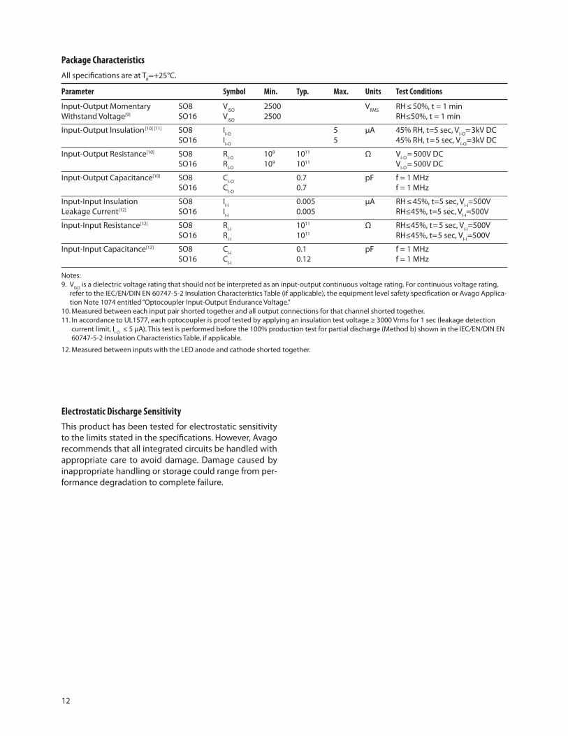
Package Characteristics
All specifications are at TA=+25°C.
Parameter Symbol Min. Typ. Max. Units Test Conditions
Input-Output Momentary SO8 VISO
2500 VRMS
RH ≤ 50%, t = 1 minWithstand Voltage[9] SO16 V
ISO 2500 RH≤50%, t = 1 min
Input-Output Insulation[10] [11] SO8 II-O
5 μA 45% RH, t=5 sec, VI-O
= 3kV DC SO16 I
I-O 5 45% RH, t=5 sec, V
I-O=3kV DC
Input-Output Resistance[10] SO8 RI-O
109 1011 Ω VI-O
= 500V DC SO16 R
I-O 109 1011 V
I-O= 500V DC
Input-Output Capacitance[10] SO8 CI-O
0.7 pF f = 1 MHz SO16 C
I-O 0.7 f = 1 MHz
Input-Input Insulation SO8 II-I
0.005 μA RH ≤ 45%, t=5 sec, VI-I
=500VLeakage Current[12] SO16 I
I-I 0.005 RH≤45%, t=5 sec, V
I-I=500V
Input-Input Resistance[12] SO8 RI-I
1011 Ω RH≤45%, t= 5 sec, VI-I
=500V SO16 R
I-I 1011 RH≤45%, t=5 sec, V
I-I=500V
Input-Input Capacitance[12] SO8 CI-I
0.1 pF f = 1 MHz SO16 C
I-I 0.12 f = 1 MHz
Electrostatic Discharge Sensitivity
This product has been tested for electrostatic sensitivity to the limits stated in the specifications. However, Avago recommends that all integrated circuits be handled with appropriate care to avoid damage. Damage caused by inappropriate handling or storage could range from per-formance degradation to complete failure.
Notes:9. V
ISO is a dielectric voltage rating that should not be interpreted as an input-output continuous voltage rating. For continuous voltage rating,
refer to the IEC/EN/DIN EN 60747-5-2 Insulation Characteristics Table (if applicable), the equipment level safety specification or Avago Applica-tion Note 1074 entitled “Optocoupler Input-Output Endurance Voltage.”
10. Measured between each input pair shorted together and all output connections for that channel shorted together.11. In accordance to UL1577, each optocoupler is proof tested by applying an insulation test voltage ≥ 3000 Vrms for 1 sec (leakage detection
current limit, II-O
≤ 5 μA). This test is performed before the 100% production test for partial discharge (Method b) shown in the IEC/EN/DIN EN 60747-5-2 Insulation Characteristics Table, if applicable.
12. Measured between inputs with the LED anode and cathode shorted together.

13
Typical Performance
0
1
2
3
4
5
6
-60 -40 -20 0 20 40 60 80 100 120
TA - TEMPERATURE - °C
ITH
- IN
PUT
THR
ESH
OLD
CU
RR
ENT
- m
A VDD = 3.3VVO = 0.6V
RL = 350Ω
RL = 1 KΩ
RL = 4 KΩ
Figure 1. Typical input threshold current vs. temperature for 3.3V operation.
0
1
2
3
4
5
6
-60 -40 -20 0 20 40 60 80 100 120
TA - TEMPERATURE - °C
ITH
- IN
PUT
THR
ESH
OLD
CU
RR
ENT
- m
A VDD = 5.0VVO = 0.6V
RL = 350Ω
RL = 1 KΩ
RL = 4 KΩ
Figure 2. Typical input threshold current vs. temperature for 5V operation.
20
30
40
50
60
70
-60 -40 -20 0 20 40 60 80 100 120
TA - TEMPERATURE - °C
IOL
- L
OW
LEV
EL O
UTP
UT
CU
RR
ENT
- m
A VDD = 3.3V
VOL = 0.6V
IF = 7.0 mA
Figure 3. Typical low level output current vs. temperature for 3.3V operation.
20
30
40
50
60
70
-60 -40 -20 0 20 40 60 80 100 120
TA - TEMPERATURE - °C
IOL-
LO
W L
EVEL
OU
TPU
T C
UR
REN
T -
mA
VDD = 5.0VVOL = 0.6V
IF = 7.0 mA
IF = 10 mA
Figure 4. Typical low level output current vs. temperature for 5V operation.
Figure 5. Typical high level output current vs. temperature for 3.3V operation.
0
5
10
15
-60 -40 -20 0 20 40 60 80 100 120
TA - TEMPERATURE - °C
I OH
- H
IGH
LEV
EL O
UTP
UT
CURR
ENT
-μA
VO = 3.3VIF = 250 μA
VDD = 3.3V
0
5
10
15
-60 -40 -20 0 20 40 60 80 100 120
TA - TEMPERATURE - °C
IOH
- HIG
H L
EVEL
OU
TPU
T C
UR
REN
T -μ
A
Figure 6. Typical high level output current vs. temperature for 5V operation.
VDD = 5.0VVO = 5.0VIF = 250 μA
0.0
0.1
0.2
0.3
0.4
0.5
0.6
0.7
0.8
-60 -40 -20 0 20 40 60 80 100 120
TA - TEMPERATURE -°C
VO
L- L
OW
LEV
EL O
UTP
UT
VOLT
AG
E -
V
IO = 13 mA
Figure 7. Typical low level output voltage vs. temperature for 3.3V operation.
VDD = 3.3VIF = 7 mA
0.0
0.1
0.2
0.3
0.4
0.5
0.6
0.7
0.8
-60 -40 -20 0 20 40 60 80 100 120
TA - TEMPERATURE -°C
VOL
- LO
W L
EVEL
OU
TPU
T VO
LTA
GE
- V
IO = 13 mA
Figure 8. Typical low level output voltage vs. temperature for 5V operation.
VDD = 5.0VIF = 7 mA
0
1
2
3
4
5
6
7
8
9
10
-60 -40 -20 0 20 40 60 80 100 120
TA - TEMPERATURE -°C
IDD
- SU
PPLY
CU
RR
ENT
PER
CH
AN
NEL
- m
A
IF = 10 mA
IF = 0 mA
Figure 9. Typical supply current per channel vs. temperature for 3.3V operation.
VDD = 3.3V
IDDL
IDDH

14
Typical Performance, continued
0
1
2
3
4
5
6
7
8
9
10
-60 -40 -20 0 20 40 60 80 100 120
TA - TEMPERATURE -°C
IDD
- SU
PPLY
CU
RREN
T PE
R CH
AN
NEL
- m
A
Figure 10. Typical supply current per channel vs. temperature for 5V operation.
IF = 10 mA
IF = 0 mA
VDD = 5.0V
IDDL
IDDH
0.001
0.01
0.1
1
10
100
1000
1.1 1.2 1.3 1.4 1.5 1.6
VF - FORWARD VOLTAGE - V
IF
+ VF
–
Figure 11. Typical input diode forward characteristics.
TA = 25°C
I F -
FO
RW
AR
D C
UR
REN
T -
mA
0
30
60
90
120
150
-60 -40 -20 0 20 40 60 80 100 120
TA - TEMPERATURE -°C
Figure 13. Typical propagation delay vs. temperature for 5V operation.
tPLH, RL = 350Ω
tPHL, RL = 350Ω
VDD = 5.0VIF = 8.0 mA
t P -
PR
OPA
GA
TIO
N D
ELA
Y -
ns
0
10
20
30
40
-60 -40 -20 0 20 40 60 80 100 120
TA - TEMPERATURE -°C
Figure 14. Typical pulse width distortion vs. temperature for 3.3V operation.
RL = 350Ω
VDD = 3.3VIF = 8.0 mA
PWD
- P
ULS
E W
IDTH
DIS
TOR
TIO
N -
ns
0
10
20
30
40
-60 -40 -20 0 20 40 60 80 100 120
TA - TEMPERATURE -°C
Figure 15. Typical pulse width distortion vs. temperature for 5V operation.
RL = 350Ω
VDD = 5.0VIF = 8.0 mA
PWD
- P
ULS
E W
IDTH
DIS
TOR
TIO
N -
ns
0
30
60
90
120
150
-60 -40 -20 0 20 40 60 80 100 120
TA - TEMPERATURE - °C
Figure 12. Typical propagation delay vs. temperature for 3.3V operation.
tPLH, RL = 350Ω
tPHL, RL = 350Ωt P -
PR
OPA
GA
TIO
N D
ELA
Y -
ns
VDD = 3.3VIF = 8.0 mA

15
Test Circuits
Figure 16. Test circuit for tPHL. t
PLH, t
F, and t
R.
1
2
3
4
8
7
6
5
1
2
3
4
8
7
6
5PULSE GEN.
Zo = 50Ω tf = tr = 5ns
INPUTMONITORING
NODE
IF
C L*
RL0.1μF
BYPASS
*CL IS APPROXIMATELY 15 pF WHICHINCLUDES PROBE AND STRAY WIRING
CAPACITANCE
3.3V or 5VACSL-6210
tPHL tPLH
INPUTIF
OUTPUTVo
1.5V
IF = 4.0 mA
IF = 8.0 mA
10% 10%
90% 90%
OUTPUT VoMONITORINGNODE
tF tR
OUTPUT VoMONITORING
NODE
R L
0.1μFBYPASS
3.3V or 5V
ACSL-6400IF
1
8 9
161
8 9
16
PULSE GEN.Zo = 50
V FF
A
B
+ _
Vcm
Vo
Vo
CM HSWITCH AT POSITION "A": IF = 0 mA
Vo (min.)
CM L
Vo (max.)
Vcm (peak)
SWITCH AT POSITION "B": IF = 8 mA
0 V
5 V
0.5 V
Figure 17. Test circuit for common mode transient immunity and typical waveforms.

16
Application Information
ON and OFF Conditions
The ACSL-6xx0 series has the ON condition defined by current, and the OFF condition defined by voltage. In order to guarantee that the optocoupler is OFF, the forward voltage across the LED must be less than or equal to 0.8 volt for the entire operating temperature range. This has direct implications for the input drive circuit. If the design uses a TTL gate to drive the input LED, then one has to ensure that the gate output voltage is sufficient to cause the forward voltage to be less than 0.8 volt. The typical threshold current for the ACSL-6xx0 series optocouplers is 2.7 mA; however, this threshold could increase over time due to the aging effects of the LED. Drive circuit arrange-ments must provide for the ON state LED forward current of at least 7 mA, or more if faster operation is desired.
Maximum Input Current and Reverse Voltage
The average forward input current should not exceed the 15 mA Absolute Maximum Rating as stated; however, peaking circuits with transient input currents up to 50 mA are allowed provided the average current does not exceed 15 mA. If the input current maximum rating is exceeded,
the local temperature of the LED can rise, which in turn may affect the long-term reliability of the device. When designing the input circuit, one must also ensure that the input reverse voltage does not exceed 5 V. If the optocoupler is subjected to reverse voltage transients or accidental situations that may cause a reverse voltage to be applied, thus an anti-parallel diode across the LED is recommended.
Suggested Input Circuits for
Driving the LED
Figures 18, 19, and 20 show some of the several techniques for driving the ACSL-6xx0 LED. Figure 18 shows the rec-ommended circuit when using any type of TTL gate. The buffer PNP transistor allows the circuit to be used with TTL or CMOS gates that have low sinking current capabil-ity. One advantage of this circuit is that there is very little variation in power supply current due to the switching of the optocoupler LED. This can be important in high-reso-lution analog-to-digital (A/D) systems where ground loop currents due to the switching of the LEDs can cause distor-tion in the A/D output.
Figure 18. TTL interface circuit for the ACSL-6xx0.

17
With a CMOS gate to drive the optocoupler, the circuit shown in Figure 19 can be used. The diode in parallel to the current limiting resistor speeds the turn-off of the optocoupler LED. Any HC or HCT series CMOS gate can be used in this circuit.
For high common-mode rejection applications, the drive circuit shown in Figure 20 is recommended. In this circuit, only an open-collector TTL, or an open drain CMOS gate can be used. This circuit drives the optocoupler LED with a 220 ohm current-limiting resistor to ensure that an I
F
of 7 mA is applied under worst case conditions and thus guarantee the 10,000 V/μs optocoupler common mode rejection rating. The designer can obtain even higher common-mode rejection performance than 10,000 V/μs by driving the LED harder than 7 mA.
Phase Relationship to Input
The output of the optocoupler is inverted when compared to the input. The input is defined to be logic HIGH when the LED is ON. If there is a design that requires the optocoupler to behave as a non-inverting gate, then
Figure 20. High CMR drive circuit for the ACSL-6xx0.
Figure 21. High voltage switching with ACSL-6xx0.
Figure 22. High voltage and high current switching
with ACSL-6xx0.
Figure 19. CMOS drive circuit for the ACSL-6xx0.
the series input drive circuit shown in Figure 19 can be used. This input drive circuit has an inverting function, and since the optocoupler also behaves as an inverter, the total circuit is non-inverting. The shunt drive circuits shown in Figures 18 and 20 will cause the optocoupler to function as an inverter.
Current and Voltage Limitations
The absolute maximum voltage allowable at the output supply voltage pin and the output voltage pin of the opt-ocoupler is 7 volts. However, the recommended maximum voltage at these two pins is 5.5 volts. The output sinking current should not exceed 13 mA in order to make the Low Level Output Voltage be less than 0.6 volt. If the output voltage is not a consideration, then the absolute maximum current allowed through the ACSL-6xx0 is 50 mA. If the output requires switching either higher currents or voltages, output buffer stages as shown in Figures 21 and 22 are suggested.

18
Propagation Delay, Pulse-Width Distortion and Propagation
Delay Skew
Propagation delay is a figure of merit which describes how quickly a logic signal propagates through a system. The propaga- tion delay from low to high (t
PLH) is the amount of time required for an input signal to
propagate to the output,causing the output to change from low to high. Similarly,the propagation delay from high to low (t
PHL) is the amount of time required for the
input signal to propagate to the output causing the output to change from high to low (see Figure 16).
Pulse-width distortion (PWD) results when tPLH
and tPHL
differ in value. PWD is defined as the difference between t
PLH and
tPHL
and often determines the maximum data rate capability of a transmission system. PWD can be expressed in percent by dividing the PWD (in ns) by the minimum pulse width (in ns) being transmitted. Typically, PWD on the order of 20-30% of the minimum pulse width is tolerable; the exact figure depends on the particular application (RS232, RS422, T-l, etc.).
Propagation delay skew,tPSK
, is an important parameter to consider in parallel data applica- tions where synchro-nization of signals on parallel data lines is a concern. If the parallel data is being sent through a group of op-tocouplers, differences in propagation delays will cause the data to arrive at the outputs of the optocouplers at different times. If this difference in propagation delays is large enough, it will determine the maximum rate at which parallel data can be sent through the optocou-plers.
Propagation delay skew is defined as the difference between the minimum and maximum propagation delays,either t
PLH or t
PHL, for any given group of optocou-
plers which are operating under the same conditions (i.e.,
the same drive current, supply voltage, output load, and operating temperature). As illustrated in Figure 23, if the inputs of a group of optocouplers are switched either ON or OFF at the same time, t
PSK is the difference between the
shortest propagation delay,either tPLH
or tPHL, and the longest propagation delay,either t
PLH or t
PHL.
As mentioned earlier,tPSK
can determine the maximum parallel data transmission rate. Figure 24 is the timing diagram of a typical parallel data application with both the clock and the data lines being sent through opto-couplers. The figure shows data and clock signals at the inputs and outputs of the optocouplers. To obtain the maximum data transmission rate, both edges of the clock signal are being used to clock the data;if only one edge were used, the clock signal would need to be twice as fast.
Propagation delay skew repre- sents the uncertainty of where an edge might be after being sent through an op-tocoupler. Figure 24 shows that there will be uncertainty in both the data and the clock lines. It is important that these two areas of uncertainty not overlap, otherwise the clock signal might arrive before all of the data outputs have settled,or some of the data outputs may start to change before the clock signal has arrived. From these considerations, the absolute minimum pulse width that can be sent through optocouplers in a parallel application is twice t
PSK. A cautious design should use a slightly longer
pulse width to ensure that any additional uncertainty in the rest of the circuit does not cause a problem.
The tPSK
specified optocouplers offer the advantages of guaranteed specifications for propagation delays, pulse-width distortion and propagation delay skew over the recommended temperature, input current, and power supply ranges.
Figure 23. Propagation delay skew – tPSK. Figure 24. Parallel data transmission example.

For product information and a complete list of distributors, please go to our web site: www.avagotech.com
Avago, Avago Technologies, and the A logo are trademarks of Avago Technologies in the United States and other countries.
Data subject to change. Copyright © 2005-2009 Avago Technologies. All rights reserved. Obsoletes 5989-2159EN
AV02-0235EN - February 5, 2009