av02-0031en,0 fiber module document
DESCRIPTION
SFP fiber moduleTRANSCRIPT

AFBR-5903Z/5903EZ/5903AZFDDI, Fast Ethernet Transceivers in 2 x 5 Package Style
Data Sheet
Features• Multisourced2x5packagestylewithMT-RJ
receptacle• Single+3.3Vpowersupply• Wavesolderandaqueouswashprocesscompatible• Fullcompliancewiththeopticalperformance
requirementsoftheFDDIPMDstandard• FullcompliancewiththeFDDILCF-PMDstandard• Fullcompliancewiththeopticalperformance
requirementsoftheATM100Mb/sphysicallayer• Fullcompliancewiththeopticalperformance
requirementsof100 Base-FXversionofIEEE802.3u• “RoHS”compliance• Receiveroutputsquelchfunctionenabled
Applications• Multimodefiberbackbonelinks• Multimodefiberwiringclosettodesktoplinks
Ordering InformationTheAFBR-5903Z1300nmproductisavailableforpro-ductionordersthroughtheAvagoTechnologiesCom-ponentFieldSalesOfficesandAuthorizedDistributorsworldwide.
AFBR-5903Z = 0°Cto+70°C NoShieldAFBR-5903EZ = 0°Cto+70°C ExtendedShieldAFBR-5903AZ = -40°Cto+85°C NoShield.
DescriptionTheAFBR-5903ZfamilyoftransceiversfromAvagoTech-nologies provide the system designer with productstoimplementarangeofFDDIandATM(AsynchronousTransferMode)designsatthe100Mb/s-125MBdrate.
The transceivers are all supplied in the new industrystandard 2 x 5 DIP style with a MT-RJ fiber connectorinterface.
FDDI PMD, ATM and Fast Ethernet 2 km Backbone LinksTheAFBR-5903Zisa1300nmproductwithopticalper-formance compliant with the FDDI PMD standard.TheFDDI PMD standard is ISO/IEC 9314-3: 1990 and ANSIX3.166-1990.
Thesetransceiversfor2kmmultimodefiberbackbonesaresupplied inthesmall2x5MT-RJpackagestyle forthose designers who want to avoid the larger MIC/R(Media Interface Connector/Receptacle) defined in theFDDIPMDstandard.
Avago Technologies also provides several other FDDIproductscompliantwiththePMDandSM-PMDstandards.TheseproductsareavailablewithMIC/R,ST©,SCandFCconnectorstyles.Theyareavailableinthe1x9,1x13and2x11transceiverand16pintransmitter/receiverpack-agestylesforthosedesignsthatrequirethesealternateconfigurations.
The AFBR-5903Z is also useful for both ATM 100 Mb/sinterfacesandFastEthernet100Base-FXinterfaces.TheATMForumUser-NetworkInterface(UNI)Standard,Version3.0,definesthePhysicalLayerfor100Mb/sMultimodeFiberInterfaceforATMinSection2.3tobetheFDDIPMDStandard.Likewise,theFastEthernetAlliancedefinesthePhysicalLayerfor100Base-FXforFastEthernettobetheFDDIPMDStandard.
ATM applications for physical layers other than 100Mb/s Multimode Fiber Interface are supported byAvago Technologies. Products are available for boththesingle-modeandthemultimodefiberSONETOC-3c(STS-3c),SDH(STM-1)ATMinterfacesandthe155Mb/s-194 MBd multimode fiber ATM interface as specifiedintheATMForumUNI.
ContactyourAvagoTechnologiessalesrepresenta-tiveforinformationonthesealternativeFDDIandATMproducts.
2
Transmitter SectionsThetransmittersectionoftheAFBR-5903Zutilizesa1300nmSurfaceEmittingInGaAsPLED.ThisLEDispackagedin the optical subassembly portion of the transmittersection.ItisdrivenbyacustomsiliconICwhichconvertsdifferentialPECLlogicsignals,ECLreferenced(shifted)toa+3.3Vsupply,intoananalogLEDdrivecurrent.
Receiver SectionsThereceiversectionoftheAFBR-5903ZutilizesanInGaAsPINphotodiodecoupledtoacustomsilicontransimped-ancepreamplifier IC. It ispackaged in theoptical sub-assemblyportionofthereceiver.
ThisPIN/preamplifiercombinationiscoupledtoacustomquantizer ICwhich provides the final pulse shaping forthelogicoutputandtheSignalDetectfunction.TheDataoutputisdifferential.TheSignalDetectoutputissingle-ended. Both Data and Signal Detect outputs are PECLcompatible, ECL referenced (shifted) to a +3.3V powersupply.Thereceiveroutputs,DataOutandDataOutBar,aresquelchedatSignalDetectDeassert.Thatis,whenthelightinputpowerdecreasestoatypical-38dBmorless,theSignalDetectDeasserts,i.e.theSignalDetectoutputgoestoaPECLlowstate.Thisforcesthereceiveroutputs,DataOutandDataOutBar togotosteadyPECL levelsHighandLowrespectively.
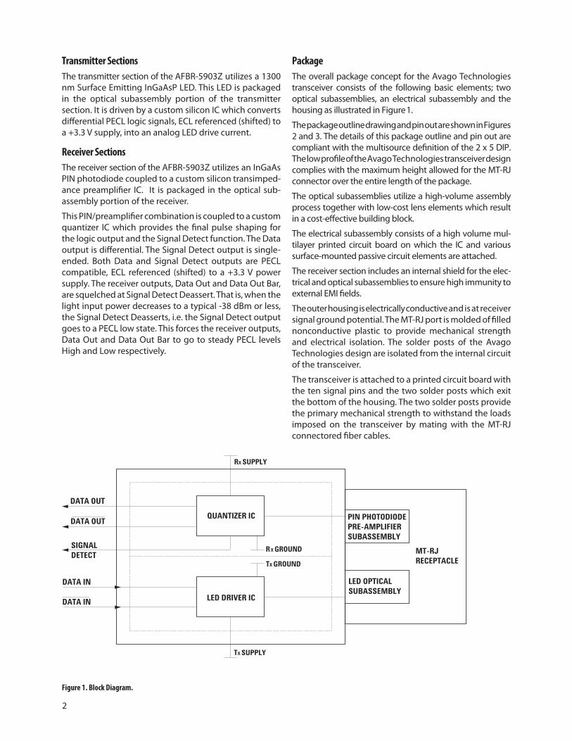
PackageTheoverallpackageconceptfortheAvagoTechnologiestransceiver consists of the following basic elements; twooptical subassemblies, an electrical subassembly and thehousingasillustratedinFigure1.
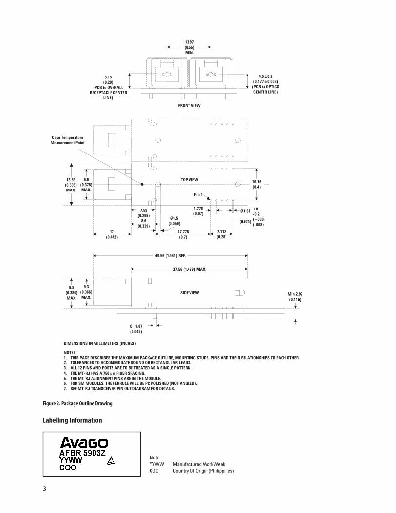
ThepackageoutlinedrawingandpinoutareshowninFigures2and3.Thedetailsofthispackageoutlineandpinoutarecompliantwiththemultisourcedefinitionofthe2x5DIP.ThelowprofileoftheAvagoTechnologiestransceiverdesigncomplieswiththemaximumheightallowedfortheMT-RJconnectorovertheentirelengthofthepackage.
Theopticalsubassembliesutilizeahigh-volumeassemblyprocesstogetherwithlow-costlenselementswhichresultinacost-effectivebuildingblock.
Theelectricalsubassemblyconsistsofahighvolumemul-tilayer printed circuit board on which the IC and varioussurface-mountedpassivecircuitelementsareattached.
Thereceiversectionincludesaninternalshieldfortheelec-tricalandopticalsubassembliestoensurehighimmunitytoexternalEMIfields.
Theouterhousingiselectricallyconductiveandisatreceiversignalgroundpotential.TheMT-RJportismoldedoffillednonconductive plastic to provide mechanical strengthand electrical isolation. The solder posts of the AvagoTechnologiesdesignareisolatedfromtheinternalcircuitofthetransceiver.
Thetransceiverisattachedtoaprintedcircuitboardwiththetensignalpinsandthetwosolderpostswhichexitthebottomofthehousing.Thetwosolderpostsprovidetheprimarymechanicalstrengthtowithstandtheloadsimposed on the transceiver by mating with the MT-RJconnectoredfibercables.
Figure 1. Block Diagram.
DATA OUT
SIGNALDETECT
DATA IN
QUANTIZER IC
LED DRIVER IC
PIN PHOTODIODEPRE-AMPLIFIERSUBASSEMBLY
LED OPTICALSUBASSEMBLY
DATA OUT
DATA IN
MT-RJRECEPTACLE
RX SUPPLY
TX SUPPLY
RX GROUND
TX GROUND
3
Figure 2. Package Outline Drawing
Note:YYWW ManufacturedWorkWeekCOO CountryOfOrigin(Philippines)
FRONT VIEW
13.97(0.55)MIN.
4.5 ±0.2(0.177 ±0.008)
(PCB to OPTICSCENTER LINE)
5.15(0.20)
(PCB to OVERALLRECEPTACLE CENTER
LINE)
DIMENSIONS IN MILLIMETERS (INCHES)
NOTES:1. THIS PAGE DESCRIBES THE MAXIMUM PACKAGE OUTLINE, MOUNTING STUDS, PINS AND THEIR RELATIONSHIPS TO EACH OTHER.2. TOLERANCED TO ACCOMMODATE ROUND OR RECTANGULAR LEADS.3. ALL 12 PINS AND POSTS ARE TO BE TREATED AS A SINGLE PATTERN.4. THE MT-RJ HAS A 750 µm FIBER SPACING.5. THE MT-RJ ALIGNMENT PINS ARE IN THE MODULE.6. FOR SM MODULES, THE FERRULE WILL BE PC POLISHED (NOT ANGLED).7. SEE MT-RJ TRANSCEIVER PIN OUT DIAGRAM FOR DETAILS.
37.56 (1.479) MAX.
SIDE VIEW
49.56 (1.951) REF.
9.8(0.386)MAX.
9.3(0.366)MAX.
Ø 1.07(0.042)
Ø 0.61
(0.024)
Pin 1
TOP VIEW9.6(0.378)MAX.
13.59(0.535)MAX.
12(0.472)
7.59(0.299)
8.6(0.339)
Ø1.5(0.059)
17.778(0.7)
1.778(0.07)
7.112(0.28)
+0-0.2(+000)(-008)
10.16(0.4)
Case TemperatureMeasurement Point
Min 2.92(0.115)
Labelling Information
4
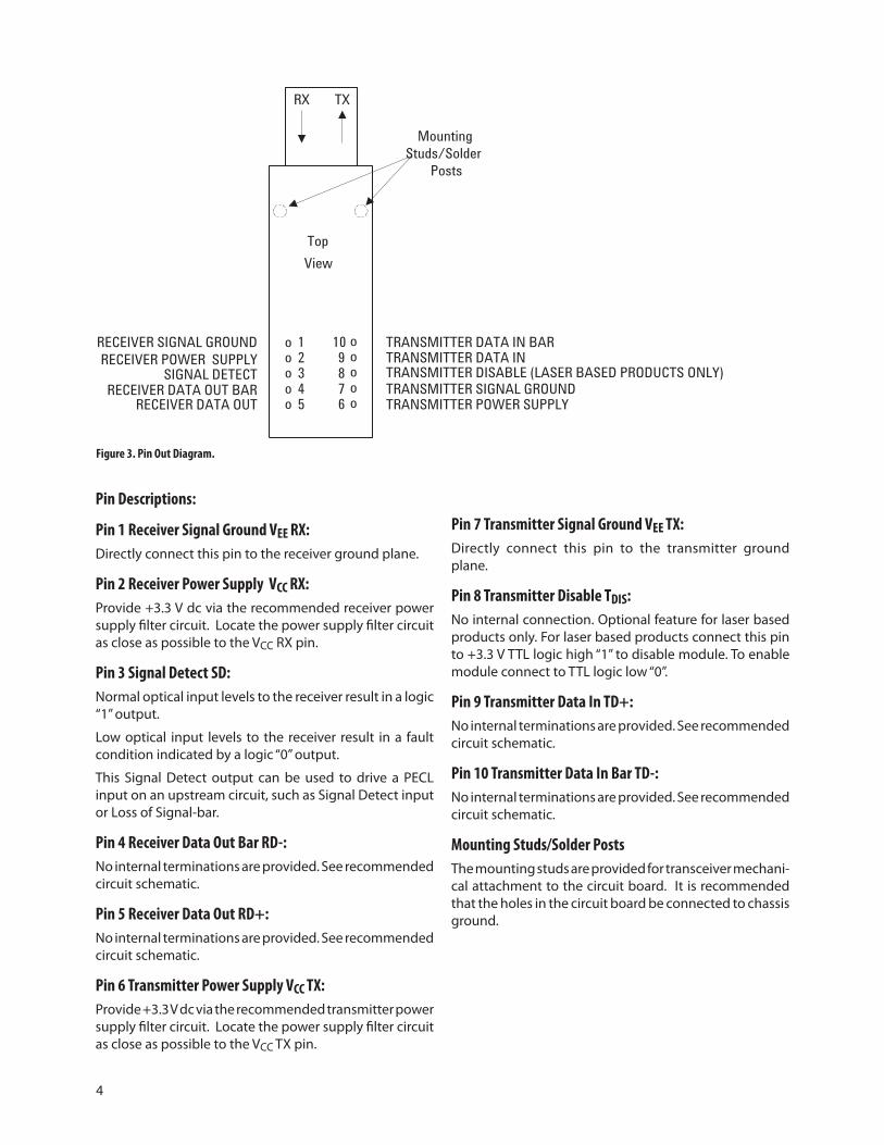
Figure 3. Pin Out Diagram.
Pin Descriptions:
Pin 1 Receiver Signal Ground VEE RX:Directlyconnectthispintothereceivergroundplane.
Pin 2 Receiver Power Supply VCC RX:Provide+3.3Vdcviatherecommendedreceiverpowersupplyfiltercircuit.LocatethepowersupplyfiltercircuitascloseaspossibletotheVCCRXpin.
Pin 3 Signal Detect SD:Normalopticalinputlevelstothereceiverresultinalogic“1”output.
Lowoptical input levels to the receiver result in a faultconditionindicatedbyalogic“0”output.
This Signal Detect output can be used to drive a PECLinputonanupstreamcircuit,suchasSignalDetectinputorLossofSignal-bar.
Pin 4 Receiver Data Out Bar RD-:Nointernalterminationsareprovided.Seerecommendedcircuitschematic.
Pin 5 Receiver Data Out RD+:Nointernalterminationsareprovided.Seerecommendedcircuitschematic.
Pin 6 Transmitter Power Supply VCC TX: Provide+3.3Vdcviatherecommendedtransmitterpowersupplyfiltercircuit.LocatethepowersupplyfiltercircuitascloseaspossibletotheVCCTXpin.
Pin 7 Transmitter Signal Ground VEE TX: Directly connect this pin to the transmitter groundplane.
Pin 8 Transmitter Disable TDIS:Nointernalconnection.Optionalfeatureforlaserbasedproductsonly.Forlaserbasedproductsconnectthispinto+3.3VTTLlogichigh“1”todisablemodule.ToenablemoduleconnecttoTTLlogiclow“0”.
Pin 9 Transmitter Data In TD+:Nointernalterminationsareprovided.Seerecommendedcircuitschematic.
Pin 10 Transmitter Data In Bar TD-: Nointernalterminationsareprovided.Seerecommendedcircuitschematic.
Mounting Studs/Solder PostsThemountingstudsareprovidedfortransceivermechani-calattachmenttothecircuitboard.Itisrecommendedthattheholesinthecircuitboardbeconnectedtochassisground.
TRANSMITTERDATAINBARTRANSMITTERDATAINTRANSMITTERDISABLE(LASERBASEDPRODUCTSONLY)TRANSMITTERSIGNALGROUNDTRANSMITTERPOWERSUPPLY
RX TX
ooooo
12345
ooooo
109876
RECEIVERSIGNALGROUNDRECEIVERPOWERSUPPLY
SIGNALDETECTRECEIVERDATAOUTBAR
RECEIVERDATAOUT
Top
View
MountingStuds/Solder
Posts
5
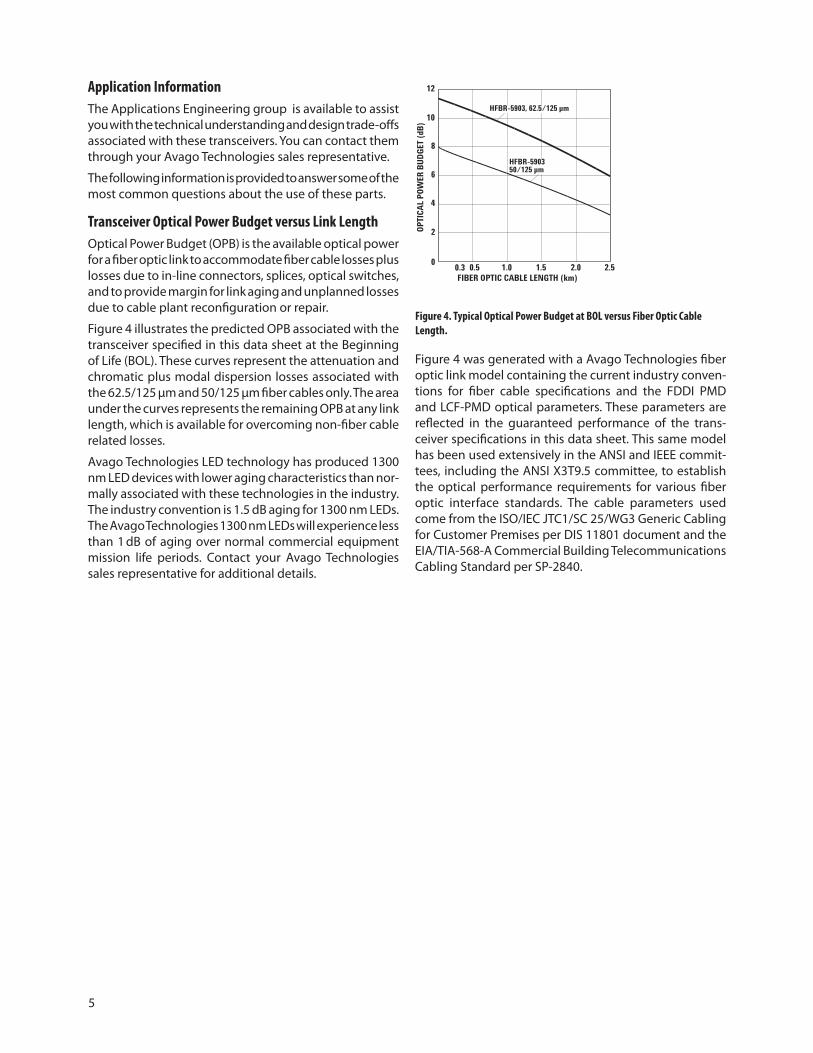
Figure 4. Typical Optical Power Budget at BOL versus Fiber Optic Cable Length.
OPT
ICA
L PO
WER
BU
DG
ET (
dB)
0
FIBER OPTIC CABLE LENGTH (km)0.5 1.5 2.0 2.5
12
10
8
6
4
2
1.00.3
HFBR-5903, 62.5/125 µm
HFBR-590350/125 µm
Application InformationTheApplicationsEngineeringgroupisavailabletoassistyouwiththetechnicalunderstandinganddesigntrade-offsassociatedwiththesetransceivers.YoucancontactthemthroughyourAvagoTechnologiessalesrepresentative.
Thefollowinginformationisprovidedtoanswersomeofthemostcommonquestionsabouttheuseoftheseparts.
Transceiver Optical Power Budget versus Link LengthOpticalPowerBudget(OPB)istheavailableopticalpowerforafiberopticlinktoaccommodatefibercablelossespluslossesduetoin-lineconnectors,splices,opticalswitches,andtoprovidemarginforlinkagingandunplannedlossesduetocableplantreconfigurationorrepair.
Figure4illustratesthepredictedOPBassociatedwiththetransceiverspecifiedinthisdatasheetattheBeginningofLife(BOL).Thesecurvesrepresenttheattenuationandchromaticplusmodaldispersionlossesassociatedwiththe62.5/125µmand50/125µmfibercablesonly.TheareaunderthecurvesrepresentstheremainingOPBatanylinklength,whichisavailableforovercomingnon-fibercablerelatedlosses.
AvagoTechnologiesLEDtechnologyhasproduced1300nmLEDdeviceswithloweragingcharacteristicsthannor-mallyassociatedwiththesetechnologiesintheindustry.Theindustryconventionis1.5dBagingfor1300nmLEDs.TheAvagoTechnologies1300nmLEDswillexperiencelessthan1dBofagingovernormalcommercialequipmentmission life periods. Contact your Avago Technologiessalesrepresentativeforadditionaldetails.
Figure4wasgeneratedwithaAvagoTechnologiesfiberopticlinkmodelcontainingthecurrentindustryconven-tions for fiber cable specifications and the FDDI PMDandLCF-PMDopticalparameters.Theseparametersarereflected in the guaranteed performance of the trans-ceiverspecificationsinthisdatasheet.ThissamemodelhasbeenusedextensivelyintheANSIandIEEEcommit-tees, includingtheANSIX3T9.5committee,toestablishthe optical performance requirements for various fiberoptic interface standards. The cable parameters usedcomefromtheISO/IECJTC1/SC25/WG3GenericCablingforCustomerPremisesperDIS11801documentandtheEIA/TIA-568-ACommercialBuildingTelecommunicationsCablingStandardperSP-2840.
6
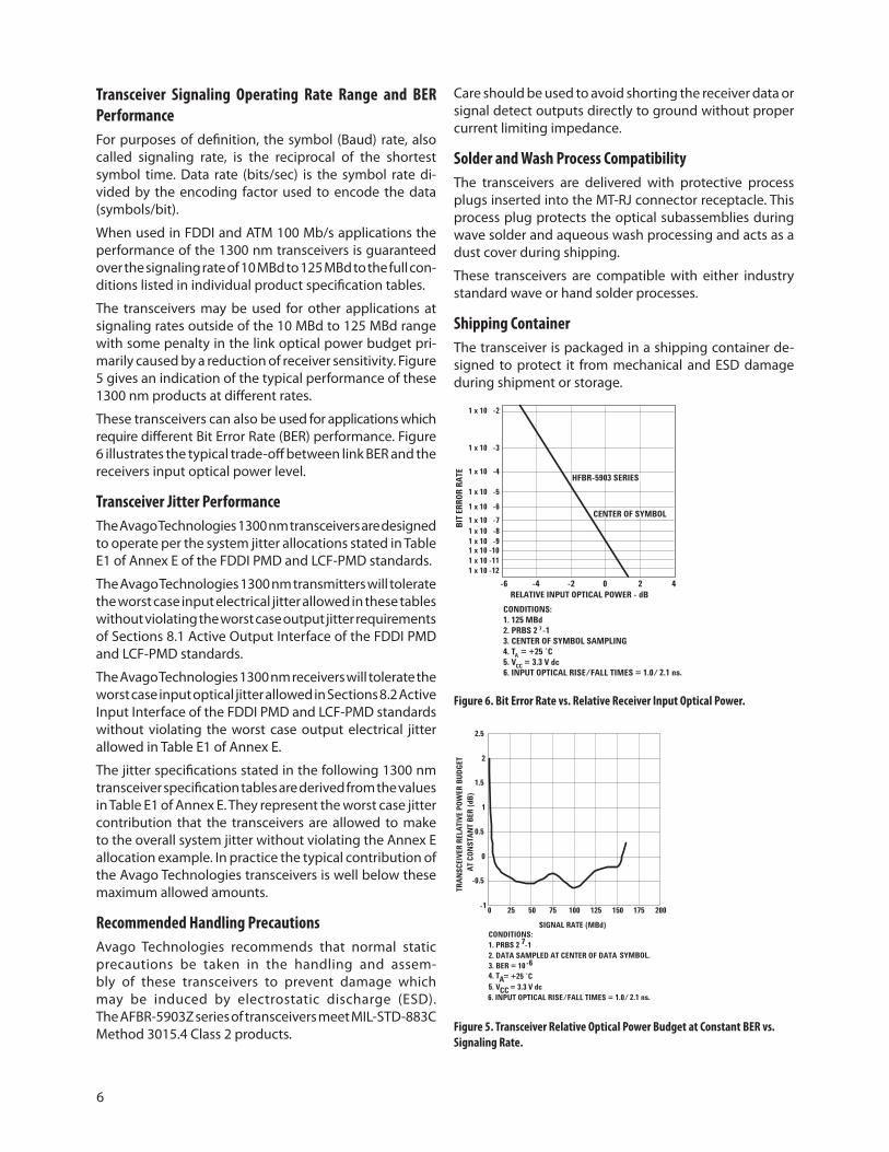
Figure 6. Bit Error Rate vs. Relative Receiver Input Optical Power.
BIT
ER
RO
R R
ATE
-6 4
1 x 10 -2
RELATIVE INPUT OPTICAL POWER - dB-4 2-2 0
1 x 10 -4
1 x 10 -6
1 x 10 -8
1 x 10 -101 x 10 -11
CONDITIONS:1. 125 MBd2. PRBS 2 7-13. CENTER OF SYMBOL SAMPLING4. TA = +25 ˚C5. VCC = 3.3 V dc6. INPUT OPTICAL RISE/FALL TIMES = 1.0/ 2.1 ns.
1 x 10 -12
1 x 10 -9
1 x 10 -7
1 x 10 -5
1 x 10 -3
CENTER OF SYMBOL
HFBR-5903 SERIES
Figure 5. Transceiver Relative Optical Power Budget at Constant BER vs. Signaling Rate.
CONDITIONS:1. PRBS 2 7-12. DATA SAMPLED AT CENTER OF DATA SYMBOL.3. BER = 10-6
4. TA = +25 ˚C5. VCC = 3.3 V dc6. INPUT OPTICAL RISE/FALL TIMES = 1.0/ 2.1 ns.
-1
-0.5
0
0.5
1
1.5
2
2.5
0 25 50 75 100 125 150 175 200
SIGNAL RATE (MBd)
TRA
NSC
EIVE
R R
ELA
TIVE
PO
WER
BU
DG
ETA
T C
ON
STA
NT
BER
(dB
)
Transceiver Signaling Operating Rate Range and BER PerformanceForpurposesofdefinition, thesymbol (Baud) rate,alsocalled signaling rate, is the reciprocal of the shortestsymbol time. Data rate (bits/sec) is the symbol rate di-vided by the encoding factor used to encode the data(symbols/bit).
WhenusedinFDDIandATM100Mb/sapplicationstheperformanceofthe1300nmtransceiversisguaranteedoverthesignalingrateof10MBdto125MBdtothefullcon-ditionslistedinindividualproductspecificationtables.
The transceivers may be used for other applications atsignalingratesoutsideofthe10MBdto125MBdrangewithsomepenaltyinthelinkopticalpowerbudgetpri-marilycausedbyareductionofreceiversensitivity.Figure5givesanindicationofthetypicalperformanceofthese1300nmproductsatdifferentrates.
ThesetransceiverscanalsobeusedforapplicationswhichrequiredifferentBitErrorRate(BER)performance.Figure6illustratesthetypicaltrade-offbetweenlinkBERandthereceiversinputopticalpowerlevel.
Transceiver Jitter PerformanceTheAvagoTechnologies1300nmtransceiversaredesignedtooperateperthesystemjitterallocationsstatedinTableE1ofAnnexEoftheFDDIPMDandLCF-PMDstandards.
TheAvagoTechnologies1300nmtransmitterswilltoleratetheworstcaseinputelectricaljitterallowedinthesetableswithoutviolatingtheworstcaseoutputjitterrequirementsofSections8.1ActiveOutputInterfaceoftheFDDIPMDandLCF-PMDstandards.
TheAvagoTechnologies1300nmreceiverswilltoleratetheworstcaseinputopticaljitterallowedinSections8.2ActiveInputInterfaceoftheFDDIPMDandLCF-PMDstandardswithout violating the worst case output electrical jitterallowedinTableE1ofAnnexE.
Thejitterspecificationsstatedinthefollowing1300nmtransceiverspecificationtablesarederivedfromthevaluesinTableE1ofAnnexE.Theyrepresenttheworstcasejittercontribution that the transceivers are allowed to maketotheoverallsystemjitterwithoutviolatingtheAnnexEallocationexample.InpracticethetypicalcontributionoftheAvagoTechnologiestransceiversiswellbelowthesemaximumallowedamounts.
Recommended Handling PrecautionsAvago Technologies recommends that normal staticprecautions be taken in the handling and assem-bly of these transceivers to prevent damage whichmay be induced by electrostatic discharge (ESD).TheAFBR-5903ZseriesoftransceiversmeetMIL-STD-883CMethod3015.4Class2products.
Careshouldbeusedtoavoidshortingthereceiverdataorsignaldetectoutputsdirectlytogroundwithoutpropercurrentlimitingimpedance.
Solder and Wash Process CompatibilityThe transceivers are delivered with protective processplugsinsertedintotheMT-RJconnectorreceptacle.Thisprocessplugprotectstheopticalsubassembliesduringwavesolderandaqueouswashprocessingandactsasadustcoverduringshipping.
These transceivers are compatible with either industrystandardwaveorhandsolderprocesses.
Shipping ContainerThetransceiverispackagedinashippingcontainerde-signed to protect it from mechanical and ESD damageduringshipmentorstorage.
7
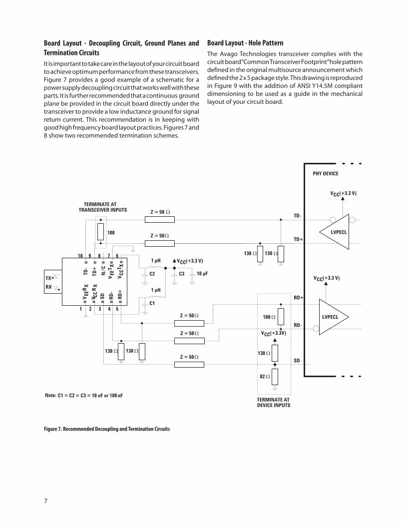
Figure 7. Recommended Decoupling and Termination Circuits
o V
EE R
Xo
V CC
RX
o S
D
o R
D-
o R
D+
Z = 50 Ω
Z = 50 Ω
TERMINATE ATTRANSCEIVER INPUTS
Z = 50 Ω
Z = 50 Ω
10 9 8 7 6
SD
LVPECL
VCC (+3.3 V)
TERMINATE ATDEVICE INPUTS
LVPECL
VCC (+3.3 V)
PHY DEVICE
TD+
TD-
RD+
RD-
VCC (+3.3V)
82 Ω
130 Ω Z = 50 Ω
1 2 3 4 5
TD-
o
TD+
o
N/C
o
VEE
TX
o
VC
C T X
o 1 µH
C2
1 µH
C1
C3 10 µF
VCC (+3.3 V)
TX
RX
Note: C1 = C2 = C3 = 10 nF or 100 nF
100
100 Ω
130 Ω 130 Ω
130 Ω 130 Ω
Board Layout - Decoupling Circuit, Ground Planes and Termination CircuitsItisimportanttotakecareinthelayoutofyourcircuitboardtoachieveoptimumperformancefromthesetransceivers.Figure 7 provides a good example of a schematic for apowersupplydecouplingcircuitthatworkswellwiththeseparts.Itisfurtherrecommendedthatacontinuousgroundplanebeprovidedinthecircuitboarddirectlyunderthetransceivertoprovidealowinductancegroundforsignalreturn current. This recommendation is in keeping withgoodhighfrequencyboardlayoutpractices.Figures7and8showtworecommendedterminationschemes.
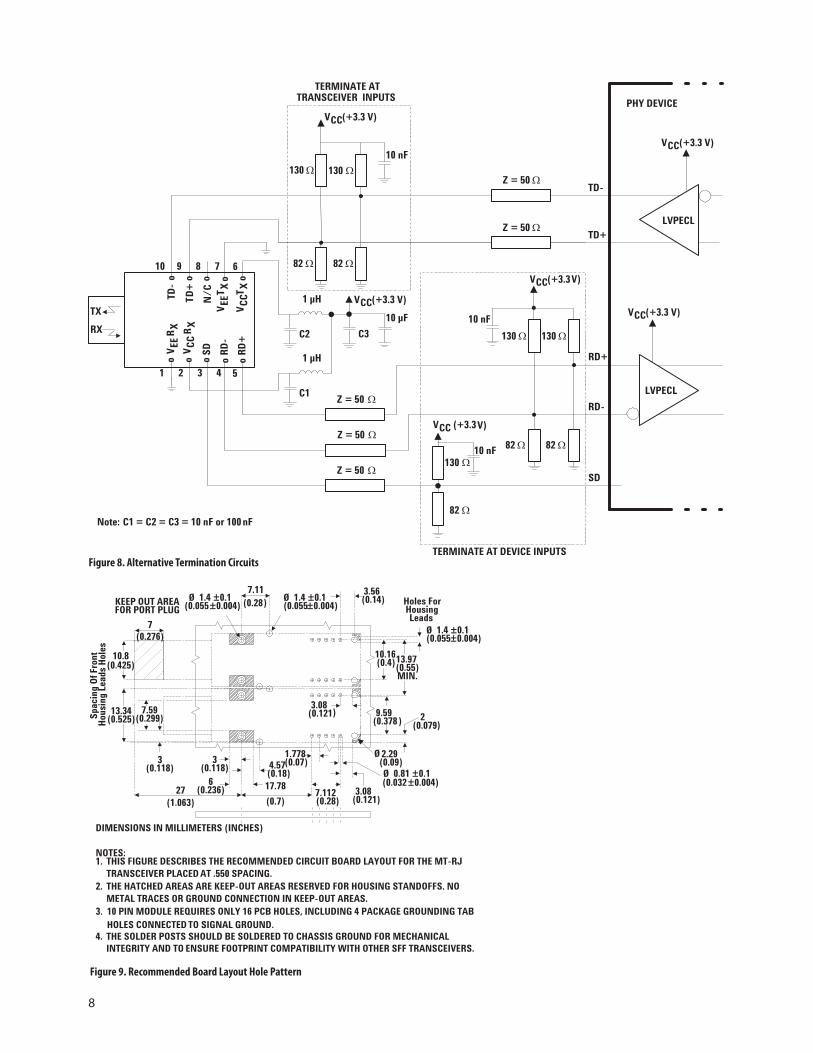
Board Layout - Hole PatternThe Avago Technologies transceiver complies with thecircuitboard“CommonTransceiverFootprint”holepatterndefinedintheoriginalmultisourceannouncementwhichdefinedthe2x5packagestyle.ThisdrawingisreproducedinFigure9withtheadditionofANSIY14.5Mcompliantdimensioning to be used as a guide in the mechanicallayoutofyourcircuitboard.
8
Figure 9. Recommended Board Layout Hole Pattern
DIMENSIONS IN MILLIMETERS (INCHES)
NOTES:1. THIS FIGURE DESCRIBES THE RECOMMENDED CIRCUIT BOARD LAYOUT FOR THE MT-RJ
TRANSCEIVER PLACED AT .550 SPACING.2. THE HATCHED AREAS ARE KEEP-OUT AREAS RESERVED FOR HOUSING STANDOFFS. NO
METAL TRACES OR GROUND CONNECTION IN KEEP-OUT AREAS.3. 10 PIN MODULE REQUIRES ONLY 16 PCB HOLES, INCLUDING 4 PACKAGE GROUNDING TAB
HOLES CONNECTED TO SIGNAL GROUND.4. THE SOLDER POSTS SHOULD BE SOLDERED TO CHASSIS GROUND FOR MECHANICAL
INTEGRITY AND TO ENSURE FOOTPRINT COMPATIBILITY WITH OTHER SFF TRANSCEIVERS.
Spac
ing
Of F
ront
Hou
sing
Lea
ds H
oles
Holes ForHousingLeads
13.34(0.525)
KEEP OUT AREAFOR PORT PLUG
7.59(0.299)
3(0.118)
3(0.118)
6(0.236)
4.57(0.18)17.78
(0.7)27
(1.063)
1.778(0.07)
7.112(0.28)
Ø 0.81 ±0.1(0.032±0.004)
3.08(0.121)
Ø 2.29(0.09)
7.11(0.28)
9.59(0.378)
3.08(0.121)
Ø 1.4 ±0.1(0.055±0.004)
Ø 1.4 ±0.1(0.055±0.004)
Ø 1.4 ±0.1(0.055±0.004)
10.16(0.4)13.97
(0.55)MIN.
3.56(0.14)
7(0.276)
10.8(0.425)
2(0.079)
Figure 8. Alternative Termination Circuits
o
VEE
RX
oV
CC
RX
o SD
o R
D-
o
RD
+
Z = 50 Ω 130 Ω
VCC (+3.3 V)
10 nF
Z = 50 Ω
130 Ω
82 Ω 82 Ω
TERMINATE ATTRANSCEIVER INPUTS
Z = 50 Ω
Z = 50 Ω
10 9 8 7 6
SD
LVPECL
VCC (+3.3 V)
TERMINATE AT DEVICE INPUTS
LVPECL
VCC (+3.3 V)
PHY DEVICE
TD+
TD-
RD+
RD-
Z = 50 Ω
1 2 3 4 5
TD-
o
TD+
o
N/C
o
VEE
TX
o
VC
C TX
o
1 µH
C2
1 µH
C1
C3
10 µF
VCC (+3.3 V)TX
RX
Note: C1 = C2 = C3 = 10 nF or 100 nF
10 nF
130 Ω
82 Ω
VCC (+3.3V)
130 Ω
82 Ω
VCC (+3.3V)
82 Ω
130 Ω 10 nF
9
Regulatory ComplianceThesetransceiverproductsareintendedtoenablecom-mercialsystemdesignerstodevelopequipmentthatcom-plieswiththevariousinternationalregulationsgoverningcertificationof InformationTechnologyEquipment.SeetheRegulatoryComplianceTable fordetails.Additionalinformation is available from your AvagoTechnologiessalesrepresentative.
Electrostatic Discharge (ESD)There are two design cases in which immunity to ESDdamageisimportant.Thefirstcaseisduringhandlingofthetransceiverpriortomountingitonthecircuitboard.ItisimportanttousenormalESDhandlingprecautionsforESDsensitivedevices.Theseprecautionsincludeusinggroundedwriststraps,workbenches,andfloormatsinESDcontrolledareas.
Thesecondcasetoconsiderisstaticdischargestotheex-terioroftheequipmentchassiscontainingthetransceiverparts.TotheextentthattheMT-RJconnectorisexposedtotheoutsideoftheequipmentchassisitmaybesubjecttowhateverESDsystemleveltestcriteriathattheequipmentisintendedtomeet.
Electromagnetic Interference (EMI)Mostequipmentdesignsutilizingthishighspeedtrans-ceiverfromAvagoTechnologieswillberequiredtomeettherequirementsofFCC intheUnitedStates,CENELECEN55022(CISPR22)inEuropeandVCCIinJapan.
ImmunityEquipmentutilizingthesetransceiverswillbesubjecttoradio-frequencyelectromagneticfieldsinsomeenviron-ments.Thesetransceivershaveahighimmunitytosuchfields.
Regulatory Compliance TableFeature Test Method Performance
ElectrostaticDischarge(ESD)totheElectricalPins
MIL-STD-883CMethod3015.4
MeetsClass2(2000to3999Volts).Withstandupto2200Vappliedbetweenelectricalpins.
ElectrostaticDischargeESD)totheMT-RJReceptacle
VariationofIEC801-2
Typicallywithstandatleast25kVwithoutdamagewhentheMT-RJConnectorReceptacleiscontactedbyaHumanBodyModelprobe.
ElectromagneticInterference(EMI)
FCCClassBCENELECCEN55022VCCIClass2
Typicallyprovidea10dBmargintothenotedstandards,however,itshouldbenotedthatfinalmargindependsonthecustomer’sboardandchasisdesign.
Immunity VariationofIEC61000-4-3Typicallyshownomeasurableeffectfroma10V/mfieldsweptfrom10to450MHzappliedtothetransceiverwhenmountedtoacircuitcardwithoutachassisenclosure.
EyeSafety IEC825Issue11993:11Class1CENELECEN60825Class1
CompliantperAvagoTechnologiestestingundersinglefaultconditions.TUVCertification:LEDClass1
RoHSCompliance ReferencetoEURoHSDirective2002/95/EC
Transceiver Reliability and Performance Qualification DataThe2x5transceivershavepassedAvagoTechnologies’reliabilityandperformancequalificationtestingandareundergoing ongoing quality and reliability monitoring.DetailsareavailablefromyourAvagoTechnologiessalesrepresentative.
Applications Support MaterialsContactyourlocalAvagoTechnologiesComponentFieldSalesOfficeforinformationonhowtoobtainevaluationboardsforthe2x5transceivers.
10
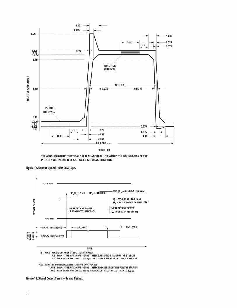
Figure 11. Transmitter Output Optical Spectral Width (FWHM) vs. Transmit-ter Output Optical Center Wavelength and Rise/Fall Times.
1380
200
100
λ - TRANSMITTER OUTPUT OPTICAL
CENTER WAVELENGTH - nm
1200 1300 1320
180
160
140
120
13601340
∆λ
- TR
AN
SMIT
TER
OU
TPU
T O
PTIC
AL
SPEC
TRA
L W
IDTH
(FW
HM
) -
nm
t r/f - TRANSMITTER
OUTPUT OPTICAL
RISE/FALL TIMES - ns
1.5
2.0
3.0
3.5
2.5
3.0
3.5
HFBR-5903 FDDI TRANSMITTER TEST RESULTSOF λC, ∆λ AND tr/f ARE CORRELATED ANDCOMPLY WITH THE ALLOWED SPECTRAL WIDTHAS A FUNCTION OF CENTER WAVELENGTH FORVARIOUS RISE AND FALL TIMES.
C
REL
ATI
VE IN
PUT
OPT
ICA
L PO
WER
(dB
)
-4 4
EYE SAMPLING TIME POSITION (ns)
-3 -1 0 1
6
3-2 2
5
4
3
2
1
0
2.5 x 10 -10 BER
1.0 x 10⁻¹² BER
CONDITIONS:
1.TA = +25 ˚C2. VCC = 3.3 V dc3. INPUT OPTICAL RISE/FALL TIMES = 1.0/2.1 ns.4. INPUT OPTICAL POWER IS NORMALIZED TO CENTER OF DATA SYMBOL.5. NOTE 19 AND 20 APPLY.
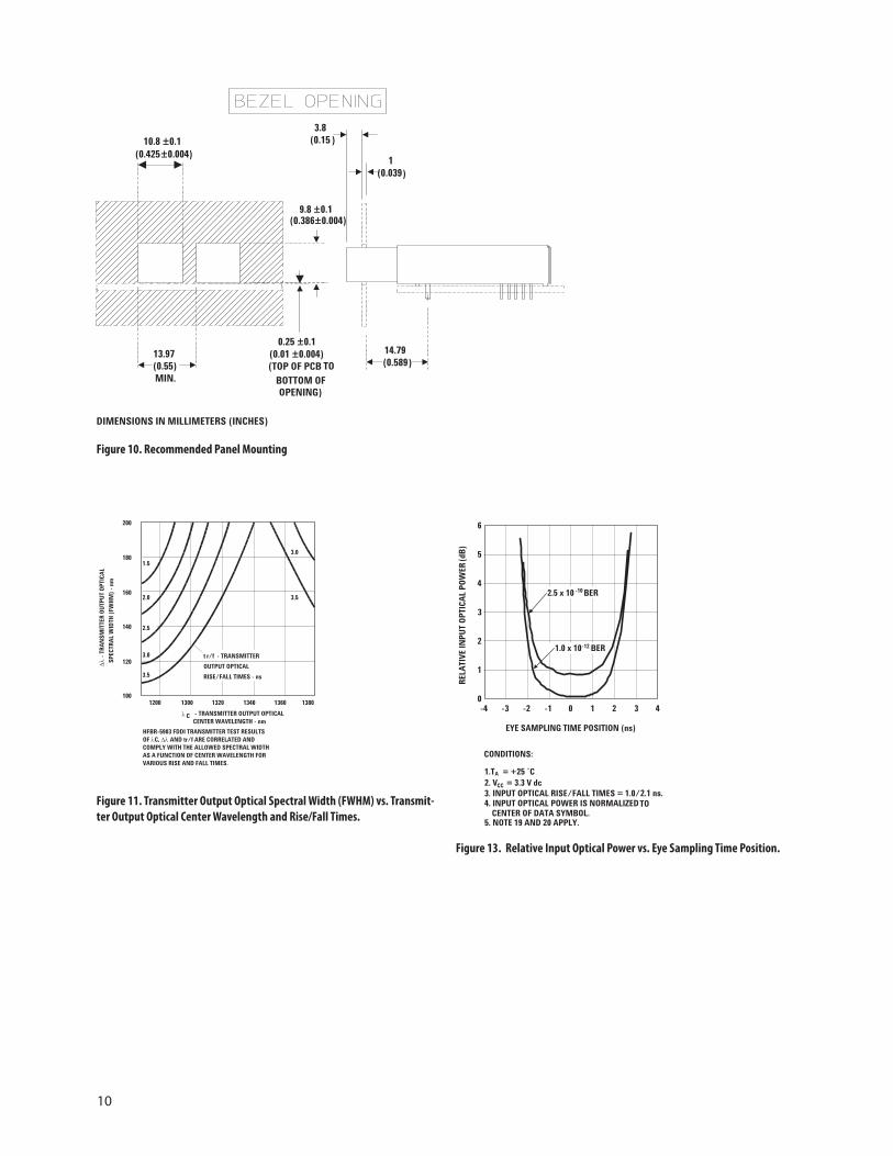
Figure 10. Recommended Panel Mounting
DIMENSIONS IN MILLIMETERS (INCHES)
10.8 ±0.1(0.425±0.004)
13.97(0.55)MIN.
0.25 ±0.1(0.01 ±0.004)
(TOP OF PCB TO
BOTTOM OFOPENING)
9.8 ±0.1(0.386±0.004)
14.79(0.589)
1(0.039)
3.8(0.15 )
Figure 13. Relative Input Optical Power vs. Eye Sampling Time Position.
11
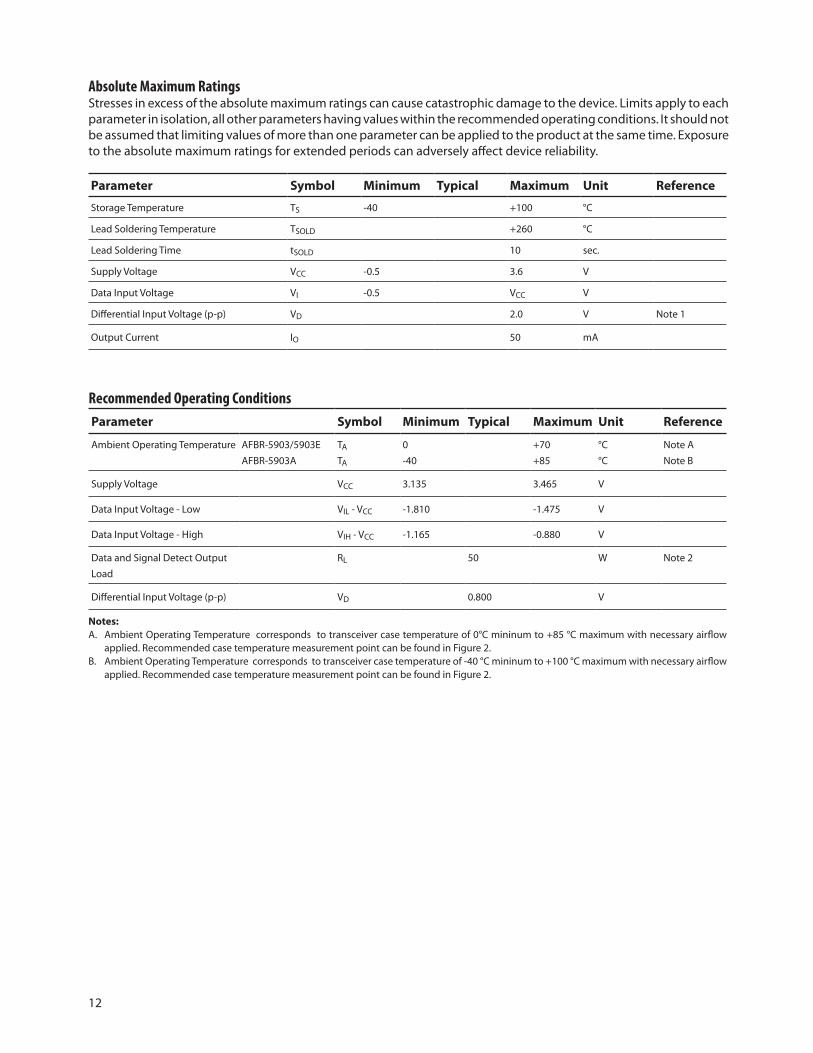
Figure 12. Output Optical Pulse Envelope.
40 ± 0.7
10.0
4.850
1.525
0.5255.6
100% TIMEINTERVAL
± 0.725 ± 0.725
4.40
1.975
0.075
0.50
0.025-
0.0250.0-
0.05
0.10
10.0
5.6 1.525
0.525
4.850
80 ± 500 ppm
4.40
1.975
0.075
0.90
1.025
1.25
TIME - ns
0% TIMEINTERVAL
1.000.975
REL
ATI
VE A
MPL
ITU
DE
THE AFBR-5903 OUTPUT OPTICAL PULSE SHAPE SHALL FIT WITHIN THE BOUNDARIES OF THEPULSE ENVELOPE FOR RISE AND FALL TIME MEASUREMENTS.
-31.0 dBm
-45.0 dBm
SIGNAL _ DETECT(ON)
SIGNAL _ DETECT (OFF)
AS _MAX
INPUT OPTICAL POWER( > 1.5 dB STEP INCREASE)
INPUT OPTICAL POWER( > 4.0 dB STEP DECREASE)
PO = MAX (PS OR -45.0 dBm)
(PS = INPUT POWER FOR BER <
102)
MIN (P O + 4.0 dB OR -31.0 dBm)P A(PO + 1.5 dB < P A < -31.0 dBm)
OPT
ICA
L PO
WER
TIME
SIG
NA
LD
ETEC
TO
UTP
UT
AS _ MAX - MAXIMUM ACQUISITION TIME (SIGNAL). AS _ MAX IS THE MAXIMUM SIGNAL _ DETECT ASSERTION TIME FOR THE STATION. AS _ MAX SHALL NOT EXCEED 100.0 µs. THE DEFAULT VALUE OF AS _ MAX IS 100.0 µs.
ANS _ MAX - MAXIMUM ACQUISITION TIME (NO SIGNAL). ANS _ MAX IS THE MAXIMUM SIGNAL _ DETECT DEASSERTION TIME FOR THE STATION. ANS _ MAX SHALL NOT EXCEED 350 µs. THE DEFAULT VALUE OF AS _ MAX IS 350 µs.
ANS _ MAX
Figure 14. Signal Detect Thresholds and Timing.
12
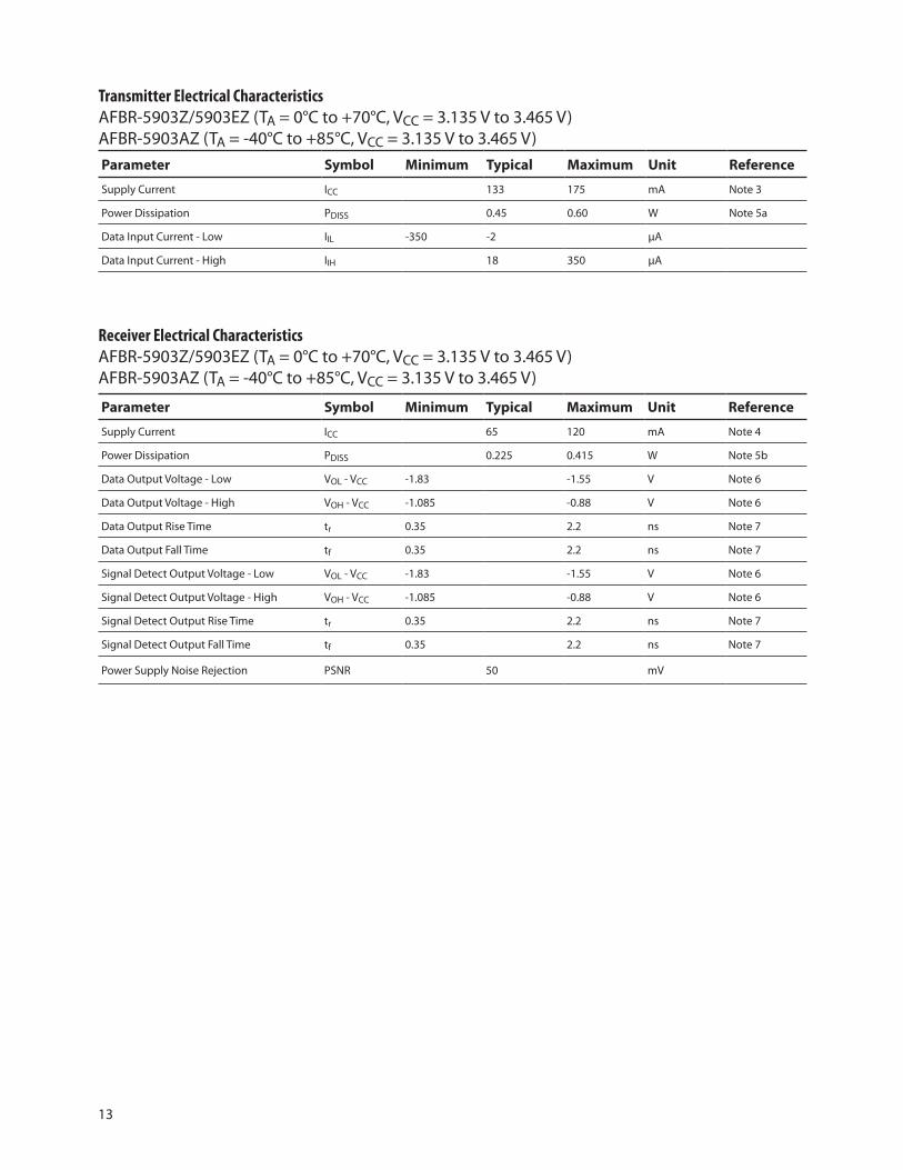
Absolute Maximum RatingsStressesinexcessoftheabsolutemaximumratingscancausecatastrophicdamagetothedevice.Limitsapplytoeachparameterinisolation,allotherparametershavingvalueswithintherecommendedoperatingconditions.Itshouldnotbeassumedthatlimitingvaluesofmorethanoneparametercanbeappliedtotheproductatthesametime.Exposuretotheabsolutemaximumratingsforextendedperiodscanadverselyaffectdevicereliability.
Parameter Symbol Minimum Typical Maximum Unit Reference
StorageTemperature TS -40 +100 °C
LeadSolderingTemperature TSOLD +260 °C
LeadSolderingTime tSOLD 10 sec.
SupplyVoltage VCC -0.5 3.6 V
DataInputVoltage VI -0.5 VCC V
DifferentialInputVoltage(p-p) VD 2.0 V Note1
OutputCurrent IO 50 mA
Parameter Symbol Minimum Typical Maximum Unit Reference
AmbientOperatingTemperature AFBR-5903/5903EAFBR-5903A
TA
TA
0-40
+70+85
°C°C
NoteANoteB
SupplyVoltage VCC 3.135 3.465 V
DataInputVoltage-Low VIL-VCC -1.810 -1.475 V
DataInputVoltage-High VIH-VCC -1.165 -0.880 V
DataandSignalDetectOutputLoad
RL 50 W Note2
DifferentialInputVoltage(p-p) VD 0.800 V
Recommended Operating Conditions
Notes:A. AmbientOperatingTemperaturecorrespondstotransceivercasetemperatureof0°Cmininumto+85°Cmaximumwithnecessaryairflow
applied.RecommendedcasetemperaturemeasurementpointcanbefoundinFigure2.B. AmbientOperatingTemperaturecorrespondstotransceivercasetemperatureof-40°Cmininumto+100°Cmaximumwithnecessaryairflow
applied.RecommendedcasetemperaturemeasurementpointcanbefoundinFigure2.
13
Parameter Symbol Minimum Typical Maximum Unit Reference
SupplyCurrent ICC 133 175 mA Note3
PowerDissipation PDISS 0.45 0.60 W Note5a
DataInputCurrent-Low IIL -350 -2 µA
DataInputCurrent-High IIH 18 350 µA
Parameter Symbol Minimum Typical Maximum Unit Reference
SupplyCurrent ICC 65 120 mA Note4
PowerDissipation PDISS 0.225 0.415 W Note5b
DataOutputVoltage-Low VOL-VCC -1.83 -1.55 V Note6
DataOutputVoltage-High VOH-VCC -1.085 -0.88 V Note6
DataOutputRiseTime tr 0.35 2.2 ns Note7
DataOutputFallTime tf 0.35 2.2 ns Note7
SignalDetectOutputVoltage-Low VOL-VCC -1.83 -1.55 V Note6
SignalDetectOutputVoltage-High VOH-VCC -1.085 -0.88 V Note6
SignalDetectOutputRiseTime tr 0.35 2.2 ns Note7
SignalDetectOutputFallTime tf 0.35 2.2 ns Note7
PowerSupplyNoiseRejection PSNR 50 mV
Receiver Electrical CharacteristicsAFBR-5903Z/5903EZ(TA=0°Cto+70°C,VCC=3.135Vto3.465V)AFBR-5903AZ(TA=-40°Cto+85°C,VCC=3.135Vto3.465V)
Transmitter Electrical CharacteristicsAFBR-5903Z/5903EZ(TA=0°Cto+70°C,VCC=3.135Vto3.465V)AFBR-5903AZ(TA=-40°Cto+85°C,VCC=3.135Vto3.465V)
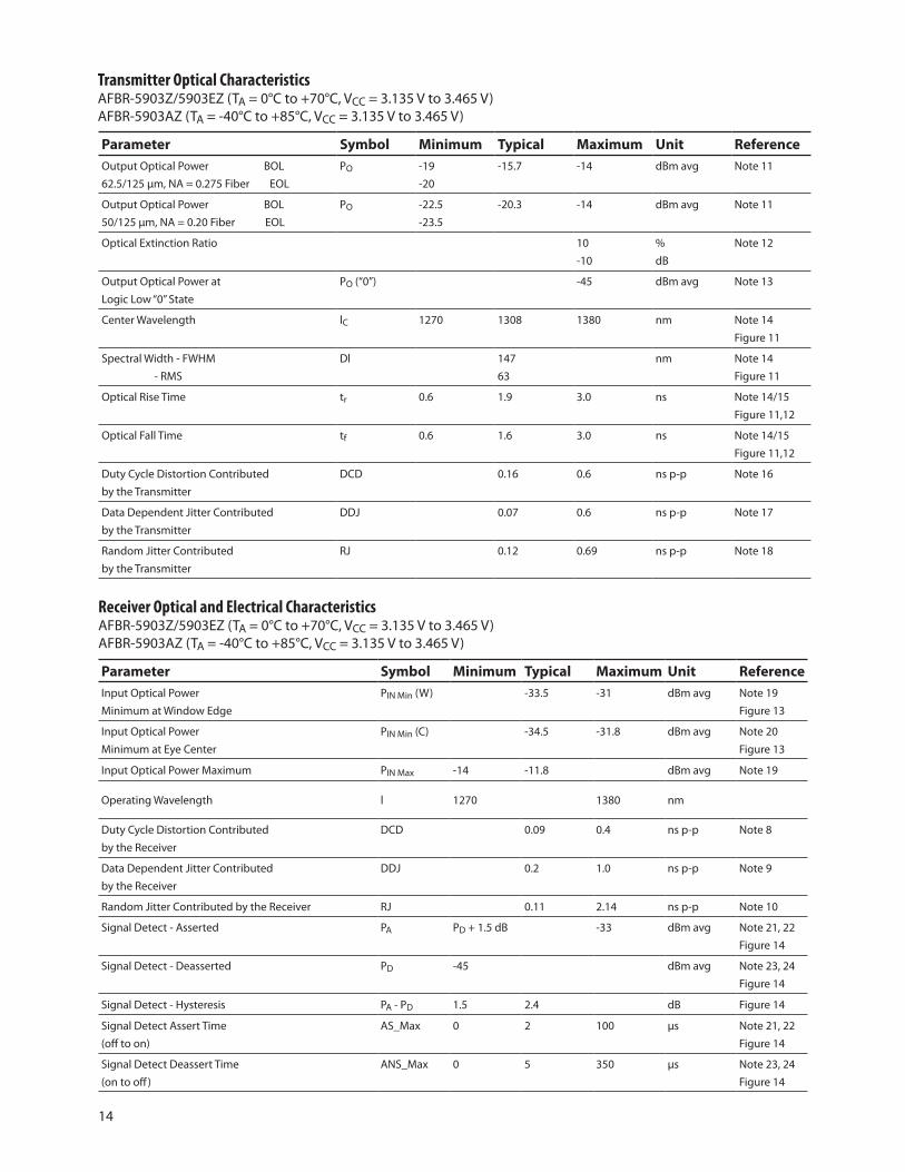
14
Receiver Optical and Electrical CharacteristicsAFBR-5903Z/5903EZ(TA=0°Cto+70°C,VCC=3.135Vto3.465V)AFBR-5903AZ(TA=-40°Cto+85°C,VCC=3.135Vto3.465V)
Parameter Symbol Minimum Typical Maximum Unit ReferenceInputOpticalPowerMinimumatWindowEdge
PINMin(W) -33.5 -31 dBmavg Note19Figure13
InputOpticalPowerMinimumatEyeCenter
PINMin(C) -34.5 -31.8 dBmavg Note20Figure13
InputOpticalPowerMaximum PINMax -14 -11.8 dBmavg Note19
OperatingWavelength l 1270 1380 nm
DutyCycleDistortionContributedbytheReceiver
DCD 0.09 0.4 nsp-p Note8
DataDependentJitterContributedbytheReceiver
DDJ 0.2 1.0 nsp-p Note9
RandomJitterContributedbytheReceiver RJ 0.11 2.14 nsp-p Note10
SignalDetect-Asserted PA PD+1.5dB -33 dBmavg Note21,22Figure14
SignalDetect-Deasserted PD -45 dBmavg Note23,24Figure14
SignalDetect-Hysteresis PA-PD 1.5 2.4 dB Figure14
SignalDetectAssertTime(offtoon)
AS_Max 0 2 100 µs Note21,22Figure14
SignalDetectDeassertTime(ontooff)
ANS_Max 0 5 350 µs Note23,24Figure14
Transmitter Optical CharacteristicsAFBR-5903Z/5903EZ(TA=0°Cto+70°C,VCC=3.135Vto3.465V)AFBR-5903AZ(TA=-40°Cto+85°C,VCC=3.135Vto3.465V)
Parameter Symbol Minimum Typical Maximum Unit ReferenceOutputOpticalPowerBOL62.5/125µm,NA=0.275FiberEOL
PO -19-20
-15.7 -14 dBmavg Note11
OutputOpticalPowerBOL50/125µm,NA=0.20FiberEOL
PO -22.5-23.5
-20.3 -14 dBmavg Note11
OpticalExtinctionRatio 10-10
%dB
Note12
OutputOpticalPoweratLogicLow“0”State
PO(“0”) -45 dBmavg Note13
CenterWavelength lC 1270 1308 1380 nm Note14Figure11
SpectralWidth-FWHM-RMS
Dl 14763
nm Note14Figure11
OpticalRiseTime tr 0.6 1.9 3.0 ns Note14/15Figure11,12
OpticalFallTime tf 0.6 1.6 3.0 ns Note14/15Figure11,12
DutyCycleDistortionContributedbytheTransmitter
DCD 0.16 0.6 nsp-p Note16
DataDependentJitterContributedbytheTransmitter
DDJ 0.07 0.6 nsp-p Note17
RandomJitterContributedbytheTransmitter
RJ 0.12 0.69 nsp-p Note18

Notes:1. ThisisthemaximumvoltagethatcanbeappliedacrosstheDifferen-
tialTransmitterData Inputs topreventdamageto the inputESDprotectioncircuit.
2. Theoutputsareterminatedwith50ΩconnectedtoVCC-2V.3. The power supply current needed to operate the transmitter is
providedtodifferentialECLcircuitry.Thiscircuitrymaintainsanearlyconstant current flow from the power supply. Constant currentoperationhelpstopreventunwantedelectricalnoisefrombeinggeneratedandconductedoremittedtoneighboringcircuitry.
4. Thisvalueismeasuredwiththeoutputsterminatedinto50Ωcon-nectedtoVCC-2Vandan InputOpticalPower levelof -14dBmaverage.
5a. Thepowerdissipationofthetransmitteriscalculatedasthesumoftheproductsofsupplyvoltageandcurrent.
5b. Thepowerdissipationofthereceiveriscalculatedasthesumoftheproductsofsupplyvoltageandcurrents,minusthesumoftheproductsoftheoutputvoltagesandcurrents.
6. ThisvalueismeasuredwithrespecttoVCCwiththeoutputterminatedinto50ΩconnectedtoVCC-2V.
7. Theoutputriseandfalltimesaremeasuredbetween20%and80%levelswiththeoutputconnectedtoVCC-2Vthrough50Ω.
8. DutyCycleDistortioncontributedbythereceiver ismeasuredatthe 50% threshold using an IDLE Line State, 125 MBd (62.5 MHzsquare-wave),inputsignal.Theinputopticalpowerlevelis-20dBmaverage.SeeApplicationInformation-TransceiverJitterSectionforfurtherinformation.
9. DataDependentJittercontributedby thereceiverisspecifiedwiththeFDDIDDJtestpatterndescribedintheFDDIPMDAnnexA.5.Theinputopticalpowerlevelis-20dBmaverage.SeeApplicationInformation-TransceiverJitterSectionforfurtherinformation.
10. RandomJittercontributedbythereceiverisspecifiedwithanIDLELineState,125MBd(62.5MHzsquare-wave),inputsignal.Theinputopticalpower level isatmaximum“PINMin. (W)”.SeeApplicationInformation-TransceiverJitterSectionforfurtherinformation.
11. Theseopticalpowervaluesaremeasuredwiththefollowingcondi-tions:• TheBeginningofLife(BOL)totheEndofLife(EOL)opticalpower
degradationistypically1.5dBpertheindustryconventionforlongwavelengthLEDs.TheactualdegradationobservedinAvagoTechnologies’1300nmLEDproductsis<1dB,asspecifiedinthisdatasheet.
• Overthespecifiedoperatingvoltageandtemperatureranges.• WithHALTLineState,(12.5MHzsquare-wave),inputsignal.• At the end of one meter of noted optical fiber with cladding
modesremoved. Theaveragepowervaluecanbeconvertedtoapeakpowervalueby
adding3dB.Higheroutputopticalpowertransmittersareavailableonspecialrequest.PleaseconsultwithyourlocalAvagoTechnologiessalesrepresentativeforfurtherdetails.
12. TheExtinctionRatioisameasureofthemodulationdepthoftheopticalsignal.Thedata“0”outputopticalpoweriscomparedtothedata“1”peakoutputopticalpowerandexpressedasapercentage.WiththetransmitterdrivenbyaHALTLineState(12.5MHzsquare-wave)signal,theaverageopticalpowerismeasured.Thedata“1”peak power is then calculated by adding 3 dB to the measuredaverageopticalpower.Thedata“0”outputopticalpowerisfoundbymeasuringtheopticalpowerwhenthetransmitterisdrivenbyalogic“0”input.Theextinctionratioistheratiooftheopticalpoweratthe“0”levelcomparedtotheopticalpoweratthe“1”levelexpressedasapercentageorindecibels.
13. ThetransmitterprovidescompliancewiththeneedforTransmit_Dis-ablecommandsfromtheFDDISMTlayerbyprovidinganOutputOpticalPowerlevelof<-45dBmaverageinresponsetoalogic“0”input.Thisspecificationappliestoeither62.5/125µmor50/125µmfibercables.
14. ThisparametercomplieswiththeFDDIPMDrequirementsforthetrade-offsbetweencenterwavelength,spectralwidth,andrise/falltimesshowninFigure11.
15. ThisparametercomplieswiththeopticalpulseenvelopefromtheFDDIPMDshowninFigure12.Theoptical riseandfall timesaremeasuredfrom10%to90%whenthetransmitterisdrivenbytheFDDIHALTLineState(12.5MHzsquare-wave)inputsignal.
16. Duty Cycle Distortion contributed by the transmitter ismeasured at a 50% threshold using an IDLE Line State,125 MBd (62.5 MHz square-wave), input signal. See ApplicationInformation -Transceiver Jitter Performance Section of this datasheetforfurtherdetails.
17. DataDependentJittercontributedbythetransmitterisspecifiedwiththeFDDItestpatterndescribedinFDDIPMDAnnexA.5.SeeApplicationInformation-TransceiverJitterPerformanceSectionofthisdatasheetforfurtherdetails.
18. RandomJittercontributedbythetransmitterisspecifiedwithanIDLELineState,125MBd(62.5MHzsquare-wave),inputsignal.SeeApplicationInformation-TransceiverJitterPerformanceSectionofthisdatasheetforfurtherdetails.
19. Thisspecification is intendedto indicatetheperformanceof thereceiversectionofthetransceiverwhenInputOpticalPowersignalcharacteristicsarepresentperthefollowingdefinitions.TheInputOpticalPowerdynamicrangefromtheminimumlevel(withawin-dowtime-width)tothemaximumlevelistherangeoverwhichthereceiverisguaranteedtoprovideoutputdatawithaBitErrorRate(BER)betterthanorequalto2.5x10-10.• AttheBeginningofLife(BOL)• Overthespecifiedoperatingtemperatureandvoltageranges• InputsymbolpatternistheFDDItestpatterndefinedinFDDIPMD
AnnexA.5with4B/5BNRZIencodeddatathatcontainsadutycyclebase-linewandereffectof50kHz.Thissequencecausesanearworstcaseconditionforinter-symbolinterference.
• Receiverdatawindowtime-widthis2.13nsorgreaterandcenteredatmid-symbol.Thisworstcasewindowtime-widthisthemini-mumallowedeye-openingpresentedtotheFDDIPHYPM_Dataindicationinput(PHYinput)pertheexampleinFDDIPMDAnnexE.Thisminimumwindowtime-widthof2.13nsisbasedupontheworstcaseFDDIPMDActiveInputInterfaceopticalcondi-tionsforpeak-to-peakDCD(1.0ns),DDJ(1.2ns)andRJ(0.76ns)presentedtothereceiver.
TotestareceiverwiththeworstcaseFDDIPMDActiveInputjitterconditionrequiresexactingcontroloverDCD,DDJandRJjittercompo-nentsthatisdifficulttoimplementwithproductiontestequipment.ThereceivercanbeequivalentlytestedtotheworstcaseFDDIPMDinputjitterconditionsandmeettheminimumoutputdatawindowtime-widthof2.13ns.Thisisaccomplishedbyusinganearlyidealinputopticalsignal(noDCD,insignificantDDJandRJ)andmeasuringforawiderwindowtime-widthof4.6ns.Thisispossibleduetothecumulativeeffectofjittercomponentsthroughtheirsuperposition(DCDandDDJaredirectlyadditiveandRJcomponentsarermsad-ditive).Specifically,whenanearlyidealinputopticaltestsignalisusedandthemaximumreceiverpeak-to-peakjittercontributionsofDCD(0.4ns),DDJ(1.0ns),andRJ(2.14ns)exist,theminimumwindowtime-widthbecomes8.0ns-0.4ns-1.0ns-2.14ns=4.46ns,orconservatively4.6ns.Thiswiderwindowtime-widthof4.6nsguaranteestheFDDIPMDAnnexEminimumwindowtime-widthof 2.13 ns under worst case input jitter conditions to the AvagoTechnologiesreceiver.• TransmitteroperatingwithanIDLELineStatepattern,125MBd
(62.5MHzsquare-wave),inputsignaltosimulateanycross-talkpresent between the transmitter and receiver sections of thetransceiver.
20. All conditions of Note 19 apply except that the measurement ismadeatthecenterofthesymbolwithnowindowtime-width.
21. Thisvalueismeasuredduringthetransitionfromlowtohighlevelsofinputopticalpower.AtSignalDetectDeassert,thereceiveroutputsDataOutandDataOutBargotosteadyPECLlevelsHighandLowrespectively.
22. TheSignalDetectoutputshallbeassertedwithin100µsafterastepincreaseoftheInputOpticalPower.ThestepwillbefromalowInputOpticalPower,-45dBm,intotherangebetweengreaterthanPA,and-14dBm.TheBERofthereceiveroutputwillbe10-2orbetterduringthetime,LS_Max(15µs)afterSignalDetecthasbeenasserted.SeeFigure14formoreinformation.
23. Thisvalueismeasuredduringthetransitionfromhightolowlevelsofinputopticalpower.Themaximumvaluewilloccurwhentheinputopticalpoweriseither-45dBmaverageorwhentheinputopticalpoweryieldsaBERof10-2orlarger,whicheverpowerishigher.
24. Signal detect output shall be de-asserted within 350 µs af-ter a step decrease in the Input Optical Power from a levelwhich is the lower of; -31 dBm or PD + 4 dB (PD is the powerlevelatwhichsignaldetectwasdeasserted),toapowerlevelof-45dBmorless.Thisstepdecreasewillhaveoccurredinlessthan8 ns.The receiver output will have a BER of 10-2 or better for aperiodof12µsoruntilsignaldetectisdeasserted.TheinputdatastreamistheQuietLineState.Also,signaldetectwillbedeassertedwithinamaximumof350µsaftertheBERofthereceiveroutputdegradesabove10-2foraninputopticaldatastreamthatdecayswithanegativerampfunctioninsteadofastepfunction.SeeFigure14formoreinformation.AtSignalDetectDeassert,thereceiveroutputsDataOutandDataOutBargotosteadyPECLlevelsHighandLowrespectively.
For product information and a complete list of distributors, please go to our web site: www.avagotech.com
Avago, Avago Technologies, and the A logo are trademarks of Avago Technologies, Limited in the United States and other countries.Data subject to change. Copyright © 2006 Avago Technologies Limited. All rights reserved. Obsoletes 5989-3084ENAV02-0031EN - July 5, 2007