atlas pixel detector for hl-lhc
DESCRIPTION
P. Morettini. ATLAS Pixel Detector for HL-LHC. High Luminosity LHC. HL-LHC will start taking data in 2025, at a levelled luminosity of 5 x 10 34 cm -2 s -1 , with the aim of collecting 3000 fb -1 . ATLAS will need a new tracker : - PowerPoint PPT PresentationTRANSCRIPT

Paolo Morettini - PIXEL 2014 1
ATLA
S
ATLAS Pixel Detector for HL-
LHC
P. Morettini
4/9/2014

Paolo Morettini - PIXEL 2014 2
ATLA
SHigh Luminosity LHCHL-LHC will start taking data in 2025, at a levelled luminosity of 5 x 1034 cm-2 s-1, with the aim of collecting 3000 fb-1.
ATLAS will need a new tracker: Progressive radiation damage and intrinsic
limitations in the FE chips will make the old detector inefficient
More granularity and more bandwidth is needed to operate at HL-LHC, due to the large pileup.
4/9/2014

ATLA
SATLAS detector upgrade plan
4/9/2014Paolo Morettini - PIXEL 2014 3
LS1 ↠ PHASE 0 ℒ = 1034cm-2s-1
<m>=24100 fb-1 (2014-2017)
LS2 ↠ PHASE 1 ℒ = 2x1034cm-2s-1
<m>=50350 fb-1 (2019-2021)
LS3 ↠ PHASE 2 ℒ =5x1034cm-2s-
1<m>=1403000 fb-1 (2023-2030)
• Installation of the 4th Pixel Detector Layer•Pixel Detector improvements•DBM beam monitor•Silicon tracker cooling system replacement•Muon EE chambers completion
• New Muon Small Wheel detector (keep same level of fakes with lumi increase)• Upgrade of the
central L1 trigger processor to allow topological L1 triggers• LAr calorimeter
electronics upgrade to increase L1 Calo granularity• Hardware track
trigger al L2 (FTK). Ussing associative memories.
• New “All Silicon” tracker• New L0-L1 trigger
schema• Inclusion of track info
in L1 trigger• Upgrade of the
calorimeter readout• Upgrade of the muon
spetrometer
LoI submittedend 2012

ATLA
SNew “All Silicon” tracker (ITk)The layout proposed in the LoI provides 14 points/track to |n| < 2.7 Pixel: 4 layers + 5 disks, 25 x 150 (in) / 50 x 150 (out)
mm2
Strips: 5 layers + 7 disks stereo Optional 5th Pixel Layer ~10 m2 of Pixels, ~200 m2 of Strips 650 M channels (Pixels), 75 M channels (Strips) 3200 10 Gb/s readout links. Same performance as the existing tracker up to m =
200
4/9/2014Paolo Morettini - PIXEL 2014 4

Paolo Morettini - PIXEL 2014 5
ATLA
SPath to the TDRThe design described in the LoI is what derives from the experience done with the existing detector and with the IBL.
But, especially in the Pixel sector, new technologies are emerging, so we want, and in some case we must, do better.
In this talk I will try to describe the options we are currently exploring in view of the preparation of a Pixel TDR in 2017.
In the TDR we will show a complete design, with a very limited number of options, ready for the pre-production phase.
4/9/2014
ProductionStripsTDR
PixelTDR
PreProduction
ITk IDRCollaboration formed
Installation
2014
2016
2017
2018-2019
2020-2022
2023-2024

Paolo Morettini - PIXEL 2014 6
ATLA
SThings we can/must improveIn the next two years, an intense R&D project will guide decisions on design and technologies, and hopefully will help us to improve on critical items: Readout speed, throughput Radiation hardness Pixel size, sensor thickness, dead zones Robustness, yield, quality control Cost
4/9/2014

Paolo Morettini - PIXEL 2014 7
ATLA
S
FE-I3
50 x 400 mm2
250 nm (IBM)
FE electronicsAt the time of the LoI, the trigger schema was a 500 kHz ROI based L0 (10% of the detector) , followed by a 200 kHz L1.
In this context, the existing FE-I4 chip was a viable solution for the outer layers.
We are now considering a full readout at 1 MHz, and this (together with the not so clear future of the IBM 130 nm process) suggests the adoption of the new 65 nm chip everywhere.
4/9/2014
FE-65
50 x 50 mm2
65 nm (TSMC)
FE-I4
50 x 250 mm2
130 nm (IBM)
0.76 cm
2.02 cm
1.8
8
cm
1.1
1
cm

Paolo Morettini - PIXEL 2014 8
ATLA
SNew FE chip design (RD53)The new generation of Pixel FE chip is currently being designed in the framework of the RD53 collaboration.
4/9/2014
• Cell size: 50x50 mm2
• Compatible with 50x50 and 25x100 mm2 pixels (staggered contacts if needed)
• TSMC 65 nm technology• Aim at 1000 e- threshold• Constant power, can operate only a
fraction of the channels• Max Pixel capacitance 100 fF (to keep the
amplifier design simple)• Advanced clustering algorithms on-chip (to
reduce bandwidth occupancy)• 2 Gb/s serial output• Full size prototype in 2 years

Paolo Morettini - PIXEL 2014 9
ATLA
SMore challages…The idea of using the new readout chip everywhere brings a number of advantages. In particular, from the trigger point of view, the possibility of a full readout at L0 opens many opportunities.
But there are side effects: A pixel size of 50x50 mm2 suggests a reduction
of the sensor thickness (less than 150 mm) and requires low noise and low threshold operation.
Signal transmission along the stave (electrically) and to the DAQ (optically) becomes even more challenging. This implies an increased R&D effort on data transmission lines and optical concentrators.
4/9/2014

Paolo Morettini - PIXEL 2014 10
ATLA
SExpected data rates
4/9/2014
From the LoI, extrapolated to 1 MHz trigger rate.
Just a rough estimates. Currently recalculating with updated geometries and pixel sizes.
The two innermost layers are obviously the critical point. Better compression mechanisms in the new chip can help.
Layer
Hits/cm2/BX
Mhits/chip @ 1 MHz
Chip output rate (Mb/s)
1 56 188 4000
2 20 67 1500
3 4 13 300
4 2 7 150

Paolo Morettini - PIXEL 2014 11
ATLA
SRead-out chain
4/9/2014
Would like to try keeping with the approach of the present Pixel Detector, where we moved as much as possible critical items and possible bottlenecks outside the detector.
But with up to 4 Gb/s per chip at 1 MHz L0, the problem can be in the electrical data transmission lines…

Paolo Morettini - PIXEL 2014 12
ATLA
SSignal transmission cables
4/9/2014
Several cables (twisted pairs, micro-coax) are under study to figure out maximum rates and lengths.
Need ~1 m to get to the end of stave, ~3-4 m to get outside.
Detailed simulations of the effect of extra material are needed.

Paolo Morettini - PIXEL 2014 13
ATLA
SReadout and trigger plansATLAS trigger schema for HL-HLT: L0 : 1 MHz - 6 ms latency L1 : 400 KHz – 24 ms latency
FE Data is transferred via fast optical links (GBT), then routed to destinations via a switched net (ETH, Infiniband…)Pixels : full readout at 1 MHz, but need to understand: Latency and resources
needed in the track trigger to cope with L1 latency.
Optical links: will a fast version of GBT be ready in time? Do we need aggregation in the inner layers?
4/9/2014

Paolo Morettini - PIXEL 2014 14
ATLA
SSensor developmentMany sensor types already in use in ATLAS:
planar, 3D, diamonds. But improvements are needed for HL-LHC: Radiation hardness Smaller pixels Thinner sensors Small edges Uniform pixel efficiency Yield Cost
4/9/2014

Paolo Morettini - PIXEL 2014 15
ATLA
SRadiation Fluences: 1 MeV neq.cm-2
Simulations with FLUKA to 3,000 fb-1
7.7MGy , 1.4x10¹⁶n
cm-2 0.9MGy , 1.7x10¹⁵n
cm-2 0.9MGy , 1.8x10¹⁵n
cm-2
4/9/2014

Paolo Morettini - PIXEL 2014 16
ATLA
SSensors: overviewPlanar: a very well known technology, being adapted to Phase II requirements.
3D: used in the IBL. More expensive than planar, but easier to handle in high fluence environments, due to lower bias voltage. Need improvements in yield.
Diamond: used in the DBM. Intrinsically rad-hard. Can operate without cooling. Expensive.
CMOS “sensor replacement”: the outsider. Lot of potential, possible cost reduction, but first of all need to be demonstrated as a technology that can be used in a large scale detector.
Many detailed, very interesting, talks in the past days 4/9/2014

Paolo Morettini - PIXEL 2014 17
ATLA
SPlanar sensor developments Bulk material (n-in-n and n-in-p, potentially
cheaper) Thin sensors (150, 100 mm or less): less
material, faster and more efficient charge collection, smaller cluster size)
Smaller pixels (25 x 500 mm2 instead of 50 x 250 tested)
Studies on slim/active edges. Full efficiency after irradiation demonstrated up
to 2 1016 neq/cm2 at 1-1.5 kV.
4/9/2014

Paolo Morettini - PIXEL 2014 18
ATLA
SBias grid tuningPunch-trough structure for the biasing is known to produce inefficiencies that become relevant with small pixels after irradiation.
Biasing with poly-silicon strips has been proved to significantly reduce these inefficiencies, especially if the routing is done avoiding the inter-implant zone.
4/9/2014
Poly-silicon resistors
Efficiency profile (almost no asymmetry)

Paolo Morettini - PIXEL 2014 19
ATLA
SQuad modules Various efforts to build and qualify “quad”
modules, i.e. single sensor tiles bonded to 4 FE-I4 chips, to be used in outer layers.
Different solutions are under test to cover the zone between the chips (long or ganged pixels).
Stress compensation layers to reduce the bow during the bump-bonding process.
4/9/2014
Micron HPK CiS

Paolo Morettini - PIXEL 2014 20
ATLA
S3D developments
4/9/2014
After the successful IBL installation, the 3D community is studying sensors optimized for HL-LHC. Small Pixels (50 x 50 preferred) Capacitance control, field simulation Thin sensors (different techniques: DWB, SOI, EPI) Slim or active edge
Thinning with DWB25 x 100 ad 50 x 50 mm2 pads positioning

Paolo Morettini - PIXEL 2014 21
ATLA
S
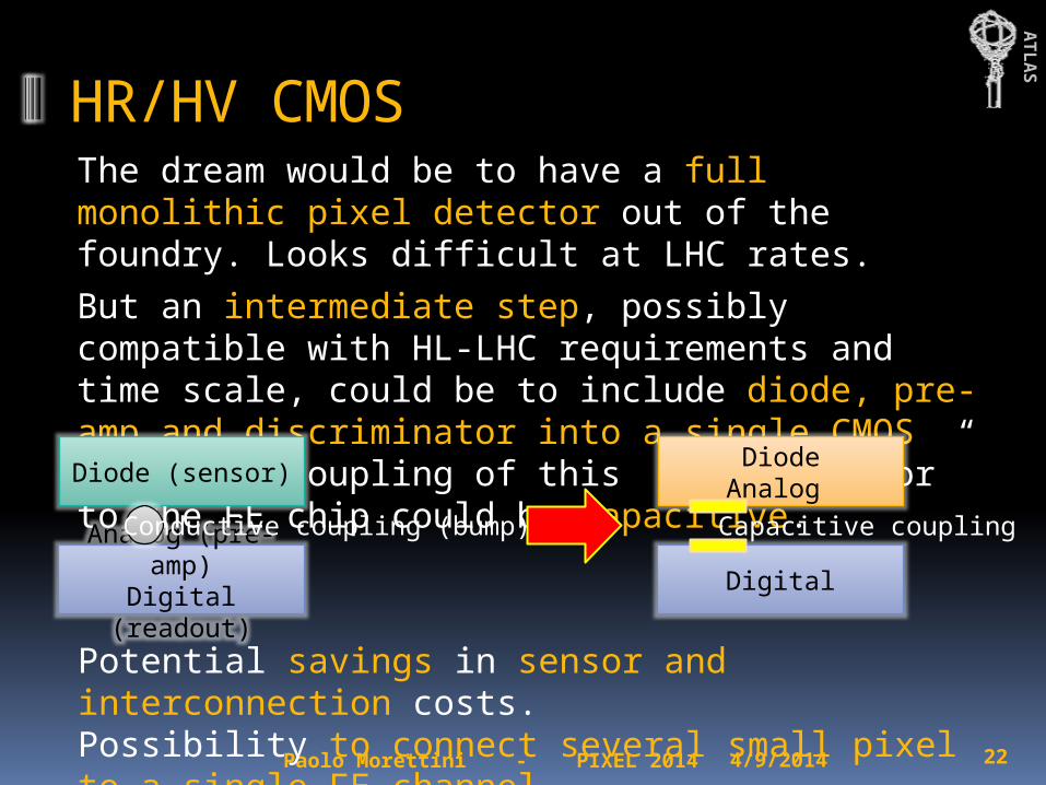
HR/HV CMOSThe dream would be to have a full monolithic pixel detector out of the foundry. Looks difficult at LHC rates.
4/9/2014
Diode (sensor)
Analog (pre-amp)
Digital (readout)
Conductive coupling (bump)DiodeAnalogDigital
Paolo Morettini - PIXEL 2014 22
ATLA
S
HR/HV CMOSThe dream would be to have a full monolithic pixel detector out of the foundry. Looks difficult at LHC rates.
But an intermediate step, possibly compatible with HL-LHC requirements and time scale, could be to include diode, pre-amp and discriminator into a single CMOS chip. The coupling of this “smart sensor” to the FE chip could be capacitive.
4/9/2014
Diode (sensor)
Analog (pre-amp)
Digital (readout)
Conductive coupling (bump)
DiodeAnalog
Digital
Capacitive coupling
Potential savings in sensor and interconnection costs.Possibility to connect several small pixel to a single FE channel.

Paolo Morettini - PIXEL 2014 23
ATLA
SHR/HV CMOS
4/9/2014
We have a number of small prototypes of CMOS “smart sensors” that can be glued to a FE-I4 and operated in a test beam or irradiation setup. Encouraging preliminary results in terms of efficiency and radiation hardness, at least up to 1015 neq/cm2.
A specific R&D is starting to evaluate this technology in time for the TDR. Full scale (FE-I4) prototype in 12-18 months. Points to clarify are:
• Charge collection efficiency• Size of the active zone• Radiation hardness• Coupling to FE• Sub-pixels• Wire-bonds on back side vs TSV• Large scale stability• Cost.

Paolo Morettini - PIXEL 2014 24
ATLA
SDetector Layout
The starting point is the LoI layout. A very traditional barrel/disk layout, based on our past experience, But the experts believe we can do better…
4/9/2014

Paolo Morettini - PIXEL 2014 25
ATLA
SPixel layouts under study
Combinations are possible…4/9/2014
Con
ical
Rin
gs
Rin
gs
ext’
d5
Pix
la
yars
Alp
ine
IBL e
xt’d

26
ATLA
SRings
Trying to facilitate service routing and to add flexibility, several options have been explored.
Disks can be replaced with independent rings, that can be positioned at different z
4/9/2014Paolo Morettini - PIXEL 2014

Paolo Morettini - PIXEL 2014 27
ATLA
SAlpineIn the Alpine layout, modules are attached to an inclined support.
Again, much more flexibility in the positioning of the individual elements and the possibility to optimize the incidence angle, hence to reduce material.
An alternative could be a conical section in the barrel…
4/9/2014

Paolo Morettini - PIXEL 2014 28
ATLA
SConicalBent staves can add flexibility in the barrel-to-endcap transition region: Can make the staves shorter, allowing a larger e
coverage and a positioning at larger radius. Incident angle closer to normal at high η (less
material, smaller clusters, less output bandwidth consumption).
4/9/2014

Paolo Morettini - PIXEL 2014 29
ATLA
SRings – High hThe studies for the extensions of the tracking in the high h region (up to = 3-4), that could be beneficial for some physics channel (e.g. VBF), are producing even more layouts. More rings can be used to cover the high rapidity regions…
4/9/2014

Paolo Morettini - PIXEL 2014 30
ATLA
SIBL extension – High h…or we could go for a very long barrel layer close to the beam pipe (like an extension of the IBL), and use the extremes of the cluster to compute Z0.
4/9/2014

Paolo Morettini - PIXEL 2014 31
ATLA
SLot of things! How to converge?How to converge to a consistent design in 2017?
We need tools to compare different options: Clear definition of the requirements, in terms of
mechanical, thermal, radiation characteristics and interfaces.
More detailed studies on servicerouting.
Performance benchmarks, possibly implemented at different simulation details (impossible to full-simulate every option).
Evaluation of prototypes. Active participation to
brainstorming and discussions Parametric cost matrix 4/9/2014

Paolo Morettini - PIXEL 2014 32
ATLA
SSummary There are many interesting ideas and new
developments on the table, and certainly this will give us the opportunity to build a better detector.
However, we are far from having a coherent design. Need to make an effort to finalize our R&D program in the next two years, in order to be able to take decisions by the TDR.
As usual, different development lines are not independent: the best detector design will emerge form the evaluation of the individual improvements in a common context.
A lot of discussion and cooperation between the groups working on sensors, readout, integration, local support and simulation will be needed.
4/9/2014

Paolo Morettini - PIXEL 2014 33
ATLA
SThe ATLAS Pixel communityThe Pixel community is completing the effort of (re)-commissioning the old detector.
A lot of experience has been accumulated, but obviously there is some conflict between the activities on the old and new detector.
However, new groups are joining, bringing in new ideas and fresh views. The community keeps growing, and is ready for the HL-LHC challenge.
4/9/2014