application note: spartan and virtex fpga families r logic ... - · pdf file2 xapp448 (v1.0)...
TRANSCRIPT
XAPP448 (v1.0) September 16, 2005 www.xilinx.com 1
© 2005 Xilinx, Inc. All rights reserved. XILINX, the Xilinx logo, and other designated brands included herein are trademarks of Xilinx, Inc. All other trademarks are the property of their respective owners.
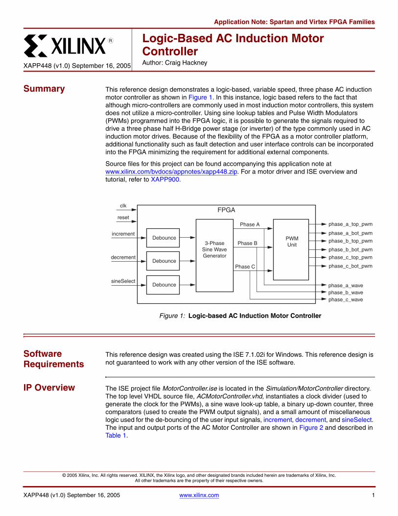
Summary This reference design demonstrates a logic-based, variable speed, three phase AC induction motor controller as shown in Figure 1. In this instance, logic based refers to the fact that although micro-controllers are commonly used in most induction motor controllers, this system does not utilize a micro-controller. Using sine lookup tables and Pulse Width Modulators (PWMs) programmed into the FPGA logic, it is possible to generate the signals required to drive a three phase half H-Bridge power stage (or inverter) of the type commonly used in AC induction motor drives. Because of the flexibility of the FPGA as a motor controller platform, additional functionality such as fault detection and user interface controls can be incorporated into the FPGA minimizing the requirement for additional external components.
Source files for this project can be found accompanying this application note at www.xilinx.com/bvdocs/appnotes/xapp448.zip. For a motor driver and ISE overview and tutorial, refer to XAPP900.
Software Requirements
This reference design was created using the ISE 7.1.02i for Windows. This reference design is not guaranteed to work with any other version of the ISE software.
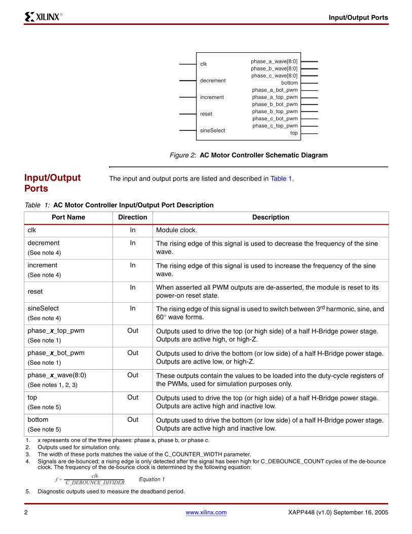
IP Overview The ISE project file MotorController.ise is located in the Simulation/MotorController directory. The top level VHDL source file, ACMotorController.vhd, instantiates a clock divider (used to generate the clock for the PWMs), a sine wave look-up table, a binary up-down counter, three comparators (used to create the PWM output signals), and a small amount of miscellaneous logic used for the de-bouncing of the user input signals, increment, decrement, and sineSelect. The input and output ports of the AC Motor Controller are shown in Figure 2 and described in Table 1.
Application Note: Spartan and Virtex FPGA Families
XAPP448 (v1.0) September 16, 2005
Logic-Based AC Induction Motor ControllerAuthor: Craig Hackney
R
Figure 1: Logic-based AC Induction Motor Controller
3-PhaseSine WaveGenerator
Debounceincrement
decrement
sineSelect
PWMUnit
Phase A
Phase B
Phase CDebounce
Debounce
clk
reset
phase_a_wavephase_b_wavephase_c_wave
phase_a_top_pwm
phase_a_bot_pwm
phase_b_top_pwm
phase_b_bot_pwm
phase_c_top_pwm
phase_c_bot_pwm
FPGA
2 www.xilinx.com XAPP448 (v1.0) September 16, 2005
Input/Output PortsR
Input/Output Ports
The input and output ports are listed and described in Table 1.
Figure 2: AC Motor Controller Schematic Diagram
phase_a_wave[8:0]phase_b_wave[8:0]phase_c_wave[8:0]
bottomphase_a_bot_pwmphase_a_top_pwmphase_b_bot_pwmphase_b_top_pwmphase_c_bot_pwmphase_c_top_pwm
top
clk
decrement
increment
reset
sineSelect
Table 1: AC Motor Controller Input/Output Port Description
Port Name Direction Description
clk In Module clock.
decrement(See note 4)
In The rising edge of this signal is used to decrease the frequency of the sine wave.
increment(See note 4)
In The rising edge of this signal is used to increase the frequency of the sine wave.
resetIn When asserted all PWM outputs are de-asserted, the module is reset to its
power-on reset state.
sineSelect(See note 4)
In The rising edge of this signal is used to switch between 3rd harmonic, sine, and 60° wave forms.
phase_x_top_pwm(See note 1)
Out Outputs used to drive the top (or high side) of a half H-Bridge power stage. Outputs are active high, or high-Z.
phase_x_bot_pwm(See note 1)
Out Outputs used to drive the bottom (or low side) of a half H-Bridge power stage. Outputs are active low, or high-Z.
phase_x_wave(8:0)(See notes 1, 2, 3)
Out These outputs contain the values to be loaded into the duty-cycle registers of the PWMs, used for simulation purposes only.
top(See note 5)
Out Outputs used to drive the top (or high side) of a half H-Bridge power stage. Outputs are active high and inactive low.
bottom(See note 5)
Out Outputs used to drive the bottom (or low side) of a half H-Bridge power stage. Outputs are active high and inactive low.
1. x represents one of the three phases: phase a, phase b, or phase c.2. Outputs used for simulation only.3. The width of these ports matches the value of the C_COUNTER_WIDTH parameter.4. Signals are de-bounced; a rising edge is only detected after the signal has been high for C_DEBOUNCE_COUNT cycles of the de-bounce
clock. The frequency of the de-bounce clock is determined by the following equation:
5. Diagnostic outputs used to measure the deadband period.
clkC_DEBOUNCE_DIVIDERf = Equation 1
Configuration Parameters
XAPP448 (v1.0) September 16, 2005 www.xilinx.com 3
R
Configuration Parameters
A number of parameters are used to configure the operation of the AC Motor Controller. The parameters are listed and described in Table 2.
Table 2: AC Motor Controller Parameter Descriptions
Parameter NameDefault Value
Valid Values Description
C_SINE_TABLE_SKIPFALSE TRUE/FALSE Selects the method of sine wave generation.
See Sine Wave Generation section for more details.
C_ACCUMULATOR_WIDTH21 0 – 32 Bit width of the accumulator used in the
generation of the sine waves See Sine Wave Generation section for more details.
C_INCREMENT_WIDTH10 1 – 16 Bit width of the register used to index the sine
tables.
C_INCREMENT241 1 – (2C_INCREMENT_WIDTH-1) Initial increment value used for sine wave
generation.
C_SINE_TYPE
0 0 – 2 Initial sinusoidal output type;
0 – Third harmonic
1 – Sine
2 – 60°
C_COUNTER_WIDTH 9 1 – 16 Width, in bits, of the PWM up-down counter.
C_DEADBAND
4 0 – (2C_COUNTER_WIDTH-1) Number of PWM clock cycles when both top and bottom PWM outputs are inactive to prevent a short circuit of the power stage. Must be 0 or divisible by 2.
C_CLOCK_DIVIDER3 1 – (232-1) Divider used to divide the clk input before it is
used to drive the PWM up-down counter.
C_ACTIVE_HIGH
TRUE TRUE/FALSE When set to TRUE the outputs of the PWM modules are high when asserted; and low when asserted if this parameter is set to FALSE. Should be set to match the polarity of the enable signals on the power stage.
C_DEBOUNCE_DIVIDER1000 1 – (232-1) Divider used to divide the clk input before it is
used to de-bounce the user input signals.
C_DEBOUNCE_COUNT16 1 – 16 Number of clock cycles
(clk/C_DEBOUNCE_DIVIDER) used to de-bounce the user input signals.
C_SIMULATIONFALSE TRUE/FALSE When set to TRUE, the phase_x_wave(8:0)
outputs are enabled.
4 www.xilinx.com XAPP448 (v1.0) September 16, 2005
SimulationR
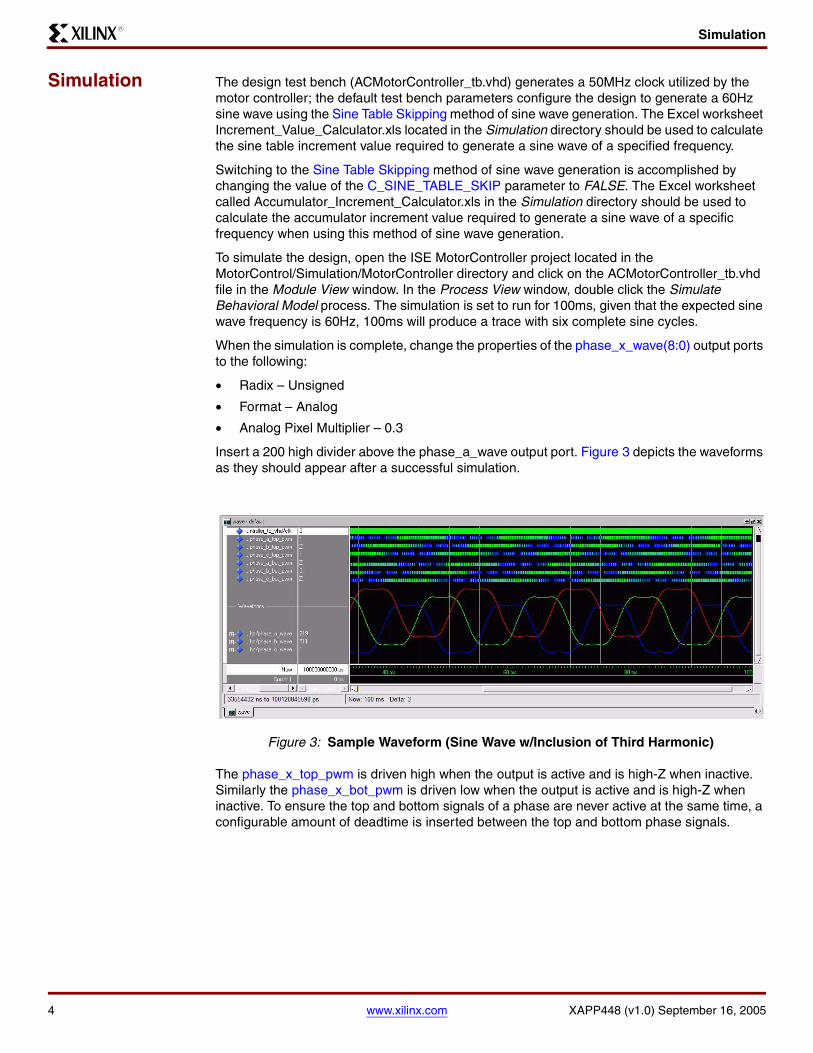
Simulation The design test bench (ACMotorController_tb.vhd) generates a 50MHz clock utilized by the motor controller; the default test bench parameters configure the design to generate a 60Hz sine wave using the Sine Table Skipping method of sine wave generation. The Excel worksheet Increment_Value_Calculator.xls located in the Simulation directory should be used to calculate the sine table increment value required to generate a sine wave of a specified frequency.
Switching to the Sine Table Skipping method of sine wave generation is accomplished by changing the value of the C_SINE_TABLE_SKIP parameter to FALSE. The Excel worksheet called Accumulator_Increment_Calculator.xls in the Simulation directory should be used to calculate the accumulator increment value required to generate a sine wave of a specific frequency when using this method of sine wave generation.
To simulate the design, open the ISE MotorController project located in the MotorControl/Simulation/MotorController directory and click on the ACMotorController_tb.vhd file in the Module View window. In the Process View window, double click the Simulate Behavioral Model process. The simulation is set to run for 100ms, given that the expected sine wave frequency is 60Hz, 100ms will produce a trace with six complete sine cycles.
When the simulation is complete, change the properties of the phase_x_wave(8:0) output ports to the following:
• Radix – Unsigned
• Format – Analog
• Analog Pixel Multiplier – 0.3
Insert a 200 high divider above the phase_a_wave output port. Figure 3 depicts the waveforms as they should appear after a successful simulation.
The phase_x_top_pwm is driven high when the output is active and is high-Z when inactive. Similarly the phase_x_bot_pwm is driven low when the output is active and is high-Z when inactive. To ensure the top and bottom signals of a phase are never active at the same time, a configurable amount of deadtime is inserted between the top and bottom phase signals.
Figure 3: Sample Waveform (Sine Wave w/Inclusion of Third Harmonic)
Simulation
XAPP448 (v1.0) September 16, 2005 www.xilinx.com 5
R
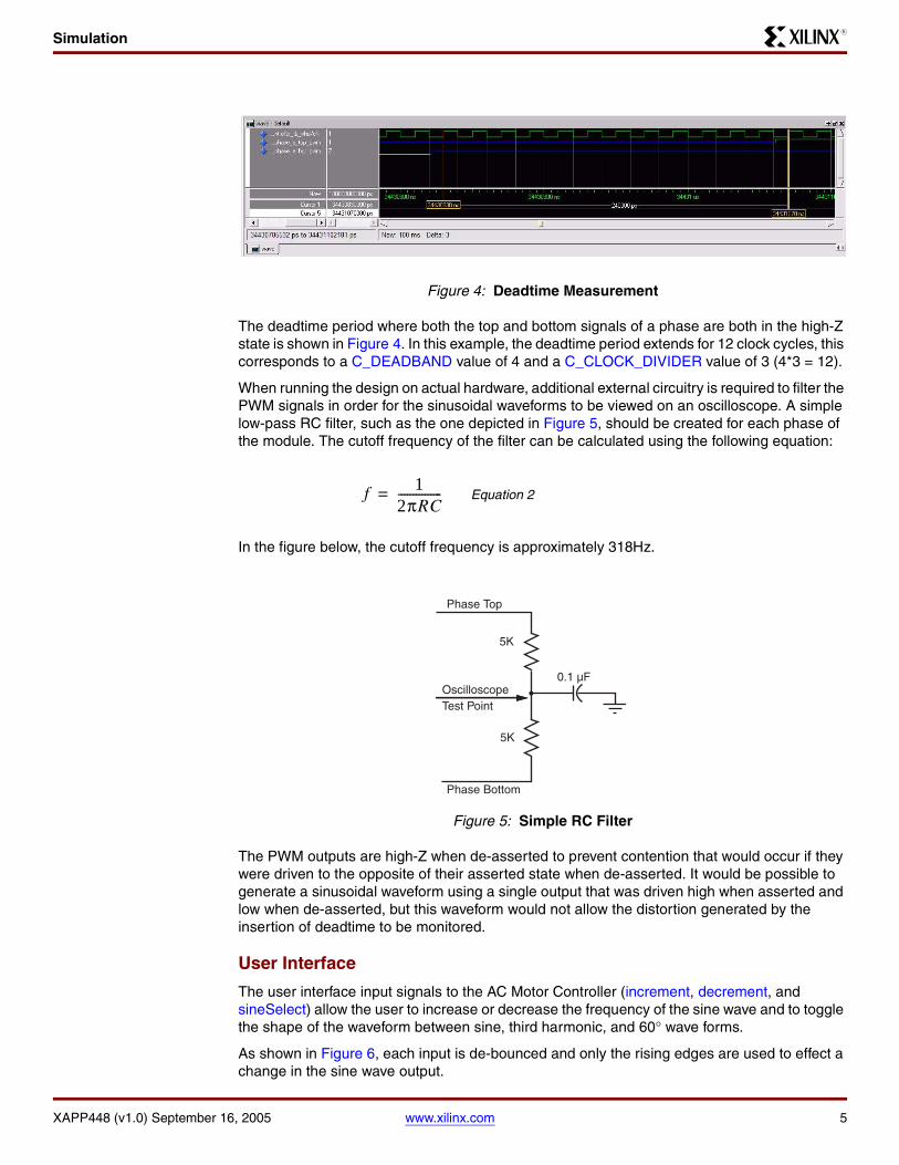
The deadtime period where both the top and bottom signals of a phase are both in the high-Z state is shown in Figure 4. In this example, the deadtime period extends for 12 clock cycles, this corresponds to a C_DEADBAND value of 4 and a C_CLOCK_DIVIDER value of 3 (4*3 = 12).
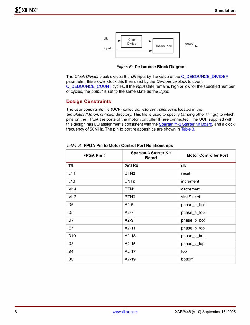
When running the design on actual hardware, additional external circuitry is required to filter the PWM signals in order for the sinusoidal waveforms to be viewed on an oscilloscope. A simple low-pass RC filter, such as the one depicted in Figure 5, should be created for each phase of the module. The cutoff frequency of the filter can be calculated using the following equation:
In the figure below, the cutoff frequency is approximately 318Hz.
The PWM outputs are high-Z when de-asserted to prevent contention that would occur if they were driven to the opposite of their asserted state when de-asserted. It would be possible to generate a sinusoidal waveform using a single output that was driven high when asserted and low when de-asserted, but this waveform would not allow the distortion generated by the insertion of deadtime to be monitored.
User Interface
The user interface input signals to the AC Motor Controller (increment, decrement, and sineSelect) allow the user to increase or decrease the frequency of the sine wave and to toggle the shape of the waveform between sine, third harmonic, and 60° wave forms.
As shown in Figure 6, each input is de-bounced and only the rising edges are used to effect a change in the sine wave output.
Figure 4: Deadtime Measurement
Figure 5: Simple RC Filter
f 12πRC---------------= Equation 2
0.1 µF
5K
5K
Phase Top
Phase Bottom
OscilloscopeTest Point
6 www.xilinx.com XAPP448 (v1.0) September 16, 2005
SimulationR
The Clock Divider block divides the clk input by the value of the C_DEBOUNCE_DIVIDER parameter, this slower clock this then used by the De-bounce block to count C_DEBOUNCE_COUNT cycles. If the input state remains high or low for the specified number of cycles, the output is set to the same state as the input.
Design Constraints
The user constraints file (UCF) called acmotorcontroller.ucf is located in the Simulation/MotorController directory. This file is used to specify (among other things) to which pins on the FPGA the ports of the motor controller IP are connected. The UCF supplied with this design has I/O assignments consistent with the Spartan™-3 Starter Kit Board, and a clock frequency of 50MHz. The pin to port relationships are shown in Table 3.
Figure 6: De-bounce Block Diagram
Table 3: FPGA Pin to Motor Control Port Relationships
FPGA Pin #Spartan-3 Starter Kit
BoardMotor Controller Port
T9 GCLK0 clk
L14 BTN3 reset
L13 BNT2 increment
M14 BTN1 decrement
M13 BTN0 sineSelect
D6 A2-5 phase_a_bot
D5 A2-7 phase_a_top
D7 A2-9 phase_b_bot
E7 A2-11 phase_b_top
D10 A2-13 phase_c_bot
D8 A2-15 phase_c_top
B4 A2-17 top
B5 A2-19 bottom
ClockDivider
De-bounce
clk
inputoutput
Pulse Width Modulators
XAPP448 (v1.0) September 16, 2005 www.xilinx.com 7
R
Pulse Width Modulators
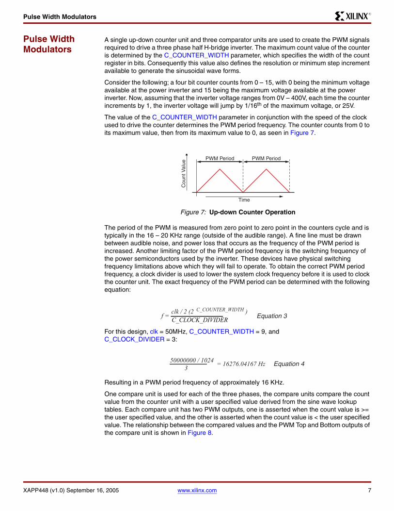
A single up-down counter unit and three comparator units are used to create the PWM signals required to drive a three phase half H-bridge inverter. The maximum count value of the counter is determined by the C_COUNTER_WIDTH parameter, which specifies the width of the count register in bits. Consequently this value also defines the resolution or minimum step increment available to generate the sinusoidal wave forms.
Consider the following; a four bit counter counts from 0 – 15, with 0 being the minimum voltage available at the power inverter and 15 being the maximum voltage available at the power inverter. Now, assuming that the inverter voltage ranges from 0V – 400V, each time the counter increments by 1, the inverter voltage will jump by 1/16th of the maximum voltage, or 25V.
The value of the C_COUNTER_WIDTH parameter in conjunction with the speed of the clock used to drive the counter determines the PWM period frequency. The counter counts from 0 to its maximum value, then from its maximum value to 0, as seen in Figure 7.
The period of the PWM is measured from zero point to zero point in the counters cycle and is typically in the 16 – 20 KHz range (outside of the audible range). A fine line must be drawn between audible noise, and power loss that occurs as the frequency of the PWM period is increased. Another limiting factor of the PWM period frequency is the switching frequency of the power semiconductors used by the inverter. These devices have physical switching frequency limitations above which they will fail to operate. To obtain the correct PWM period frequency, a clock divider is used to lower the system clock frequency before it is used to clock the counter unit. The exact frequency of the PWM period can be determined with the following equation:
For this design, clk = 50MHz, C_COUNTER_WIDTH = 9, and C_CLOCK_DIVIDER = 3:
Resulting in a PWM period frequency of approximately 16 KHz.
One compare unit is used for each of the three phases, the compare units compare the count value from the counter unit with a user specified value derived from the sine wave lookup tables. Each compare unit has two PWM outputs, one is asserted when the count value is >= the user specified value, and the other is asserted when the count value is < the user specified value. The relationship between the compared values and the PWM Top and Bottom outputs of the compare unit is shown in Figure 8.
Figure 7: Up-down Counter Operation
Time
Cou
nt V
alue
PWM Period PWM Period
f = clk / 2 (2 C_COUNTER_WIDTH )C_CLOCK_DIVIDER Equation 3
50000000 / 10243 = 16276.04167 Hz Equation 4
8 www.xilinx.com XAPP448 (v1.0) September 16, 2005
Pulse Width ModulatorsR
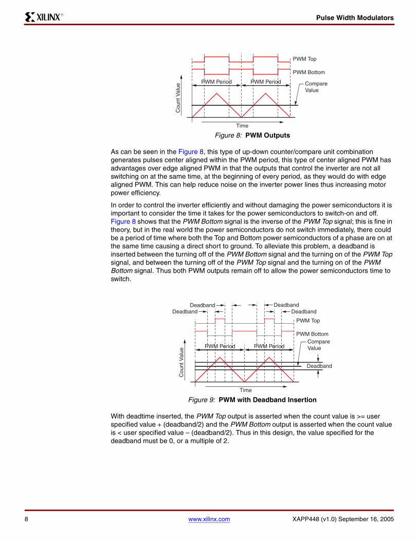
As can be seen in the Figure 8, this type of up-down counter/compare unit combination generates pulses center aligned within the PWM period, this type of center aligned PWM has advantages over edge aligned PWM in that the outputs that control the inverter are not all switching on at the same time, at the beginning of every period, as they would do with edge aligned PWM. This can help reduce noise on the inverter power lines thus increasing motor power efficiency.
In order to control the inverter efficiently and without damaging the power semiconductors it is important to consider the time it takes for the power semiconductors to switch-on and off. Figure 8 shows that the PWM Bottom signal is the inverse of the PWM Top signal; this is fine in theory, but in the real world the power semiconductors do not switch immediately, there could be a period of time where both the Top and Bottom power semiconductors of a phase are on at the same time causing a direct short to ground. To alleviate this problem, a deadband is inserted between the turning off of the PWM Bottom signal and the turning on of the PWM Top signal, and between the turning off of the PWM Top signal and the turning on of the PWM Bottom signal. Thus both PWM outputs remain off to allow the power semiconductors time to switch.
With deadtime inserted, the PWM Top output is asserted when the count value is >= user specified value + (deadband/2) and the PWM Bottom output is asserted when the count value is < user specified value – (deadband/2). Thus in this design, the value specified for the deadband must be 0, or a multiple of 2.
Figure 8: PWM Outputs
Figure 9: PWM with Deadband Insertion
Time
Cou
nt V
alue
PWM Period PWM Period
PWM Top
PWM Bottom
Compare Value
Time
Cou
nt V
alue
PWM Period PWM PeriodCompare Value
PWM Top
PWM Bottom
DeadbandDeadband
Deadband
DeadbandDeadband
Sine Wave Generation
XAPP448 (v1.0) September 16, 2005 www.xilinx.com 9
R
Sine Wave Generation
Two different methods of sine wave generation are supported by this design;
• Sine table skipping
• Variable clocking
Both methods require the creation of a sine lookup table; the values contained in this lookup table are created by a program called sinegen which is located in the Bin directory of this reference design. The sinegen program outputs three different sine lookup tables (sine, third harmonic, and 60°); each table contains 360° of the sine wave and has 256 entries, with each entry being 16-bits wide. The three sine waves required (each 120° out of phase from the others) are created by using three separate indexes into the lookup table, one for each phase.
The process by which an integer based sine lookup table is created is by no means perfect, as can be seen in Figure 11. Distortion of the sine wave begins as soon as it enters the digital domain.
Sine Table Skipping
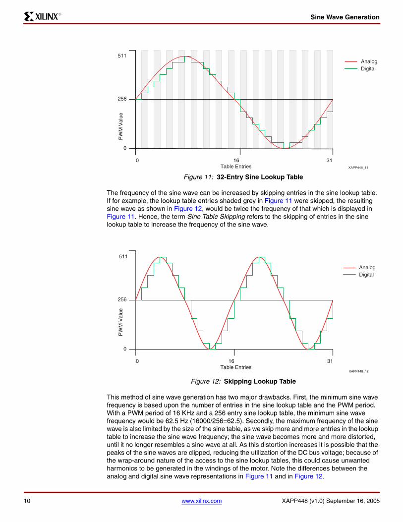
Enabled by setting the C_SINE_TABLE_SKIP parameter to TRUE, this method of sine wave generation employs a static 256 entry lookup table that contains 360° of a sine wave. By reading values from the table in sequence and passing them to the PWMs, it is possible to generate a sinusoidal output. Figure 11 depicts a 32-entry sine lookup table with 9-bit PWM values, the red line represents the analog sine wave, and the green line is the digital representation of this sine wave.
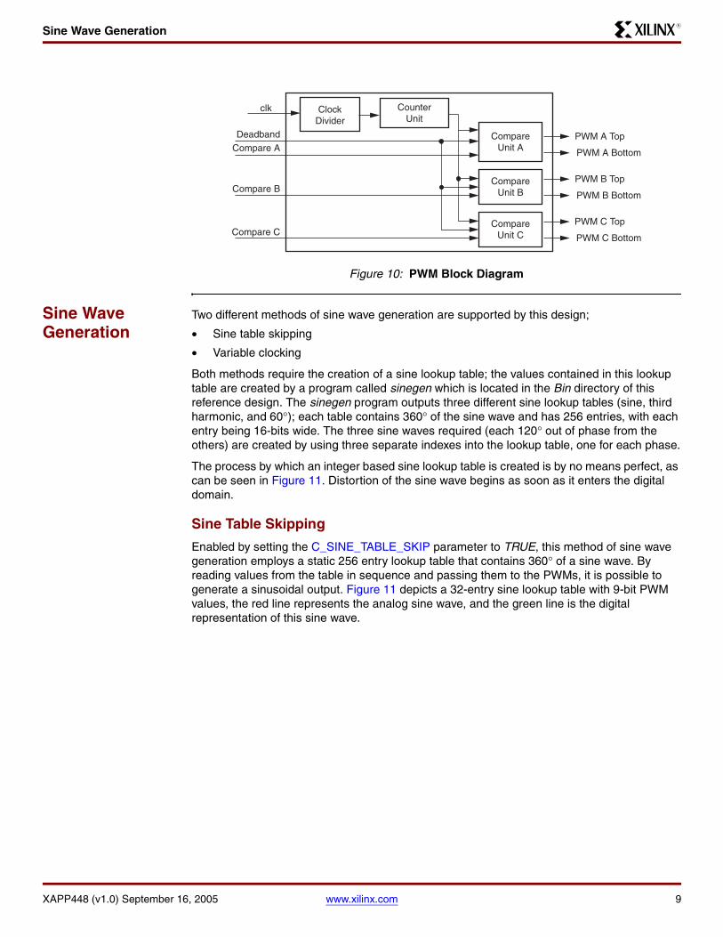
Figure 10: PWM Block Diagram
CounterUnit
ClockDivider
Deadband
Compare B
Compare A
Compare C
CompareUnit A
clk
PWM A Top
PWM A Bottom
CompareUnit B
PWM B Top
PWM B Bottom
CompareUnit C
PWM C Top
PWM C Bottom
10 www.xilinx.com XAPP448 (v1.0) September 16, 2005
Sine Wave GenerationR
The frequency of the sine wave can be increased by skipping entries in the sine lookup table. If for example, the lookup table entries shaded grey in Figure 11 were skipped, the resulting sine wave as shown in Figure 12, would be twice the frequency of that which is displayed in Figure 11. Hence, the term Sine Table Skipping refers to the skipping of entries in the sine lookup table to increase the frequency of the sine wave.
This method of sine wave generation has two major drawbacks. First, the minimum sine wave frequency is based upon the number of entries in the sine lookup table and the PWM period. With a PWM period of 16 KHz and a 256 entry sine lookup table, the minimum sine wave frequency would be 62.5 Hz (16000/256=62.5). Secondly, the maximum frequency of the sine wave is also limited by the size of the sine table, as we skip more and more entries in the lookup table to increase the sine wave frequency; the sine wave becomes more and more distorted, until it no longer resembles a sine wave at all. As this distortion increases it is possible that the peaks of the sine waves are clipped, reducing the utilization of the DC bus voltage; because of the wrap-around nature of the access to the sine lookup tables, this could cause unwanted harmonics to be generated in the windings of the motor. Note the differences between the analog and digital sine wave representations in Figure 11 and in Figure 12.
Figure 11: 32-Entry Sine Lookup Table
Figure 12: Skipping Lookup Table
31 0 16
0
256
511
PW
M V
alue
Table Entries
AnalogDigital
XAPP448_11
0 16
0
256
PW
M V
alue
Table Entries 31
511
AnalogDigital
XAPP448_12
Sine Wave Generation
XAPP448 (v1.0) September 16, 2005 www.xilinx.com 11
R
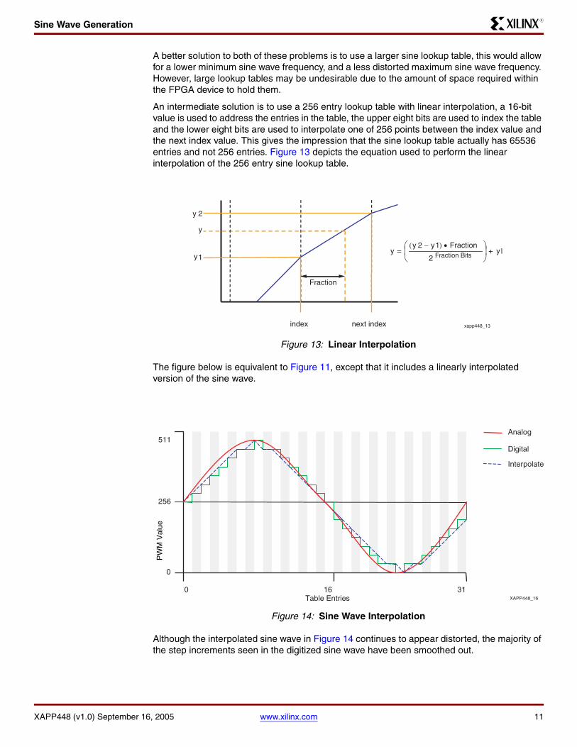
A better solution to both of these problems is to use a larger sine lookup table, this would allow for a lower minimum sine wave frequency, and a less distorted maximum sine wave frequency. However, large lookup tables may be undesirable due to the amount of space required within the FPGA device to hold them.
An intermediate solution is to use a 256 entry lookup table with linear interpolation, a 16-bit value is used to address the entries in the table, the upper eight bits are used to index the table and the lower eight bits are used to interpolate one of 256 points between the index value and the next index value. This gives the impression that the sine lookup table actually has 65536 entries and not 256 entries. Figure 13 depicts the equation used to perform the linear interpolation of the 256 entry sine lookup table.
The figure below is equivalent to Figure 11, except that it includes a linearly interpolated version of the sine wave.
Although the interpolated sine wave in Figure 14 continues to appear distorted, the majority of the step increments seen in the digitized sine wave have been smoothed out.
Figure 13: Linear Interpolation
Figure 14: Sine Wave Interpolation
Fraction
1y
2y
y
index next index
12
)12(y
Fractionyyy
Fraction Bits+⎟⎠⎞
⎜⎝⎛ •−
=
xapp448_13
31 0 16
0
256
511
PW
M V
alue
Table Entries
Analog
Digital
Interpolate
XAPP448_16
12 www.xilinx.com XAPP448 (v1.0) September 16, 2005
Sine Wave GenerationR
The value used to step though the sine table is combined with the current angle value to determine the next entry to be read from the sine lookup table (y2). The most significant bits of the angle are used to determine the current entry to be read from the sine lookup table (y1). Using y1, y2 and the least significant bits from the angle, the point (y) is interpolated.
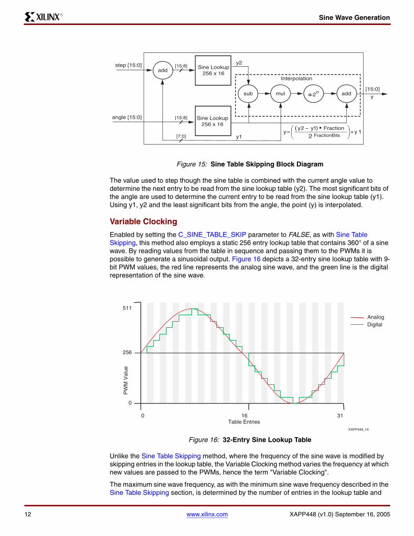
Variable Clocking
Enabled by setting the C_SINE_TABLE_SKIP parameter to FALSE, as with Sine Table Skipping, this method also employs a static 256 entry lookup table that contains 360° of a sine wave. By reading values from the table in sequence and passing them to the PWMs it is possible to generate a sinusoidal output. Figure 16 depicts a 32-entry sine lookup table with 9-bit PWM values, the red line represents the analog sine wave, and the green line is the digital representation of the sine wave.
Unlike the Sine Table Skipping method, where the frequency of the sine wave is modified by skipping entries in the lookup table, the Variable Clocking method varies the frequency at which new values are passed to the PWMs, hence the term "Variable Clocking".
The maximum sine wave frequency, as with the minimum sine wave frequency described in the Sine Table Skipping section, is determined by the number of entries in the lookup table and
Figure 15: Sine Table Skipping Block Diagram
Figure 16: 32-Entry Sine Lookup Table
12
)12(y
Fractionyyy
FractionBits+⎟⎠⎞
⎜⎝⎛ •−
=
Sine Lookup256 x 16
Sine Lookup256 x 16
sub mul add
addstep [15:0]
angle [15:0]
Interpolation
[15:0]
[15:8]
[15:8]
[7:0]
y2
y1
y2n
31 0 16
0
256
511
PW
M V
alue
Table Entries XAPP448_16
AnalogDigital
Sine Wave Generation
XAPP448 (v1.0) September 16, 2005 www.xilinx.com 13
R
PWM period. For example, with a PWM period of 16 KHz and a 256 entry sine lookup table, the maximum sine wave frequency would be 62.5 Hz (16000/256=62.5). If values are read from the lookup table at a rate that is faster than the PWM period they will effectively be skipped, since the PWMs only load a new value at the beginning of each PWM period. In this case we fall victim to the same type of wave form distortions as described in the Sine Table Skipping section.
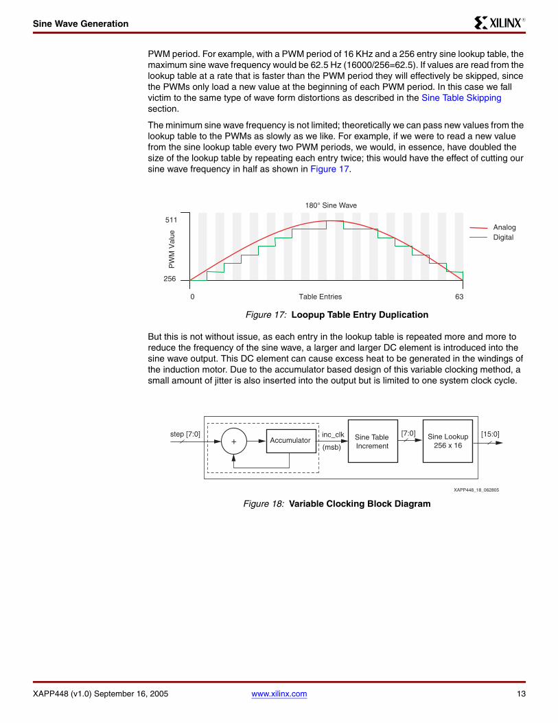
The minimum sine wave frequency is not limited; theoretically we can pass new values from the lookup table to the PWMs as slowly as we like. For example, if we were to read a new value from the sine lookup table every two PWM periods, we would, in essence, have doubled the size of the lookup table by repeating each entry twice; this would have the effect of cutting our sine wave frequency in half as shown in Figure 17.
But this is not without issue, as each entry in the lookup table is repeated more and more to reduce the frequency of the sine wave, a larger and larger DC element is introduced into the sine wave output. This DC element can cause excess heat to be generated in the windings of the induction motor. Due to the accumulator based design of this variable clocking method, a small amount of jitter is also inserted into the output but is limited to one system clock cycle.
Figure 17: Loopup Table Entry Duplication
Figure 18: Variable Clocking Block Diagram
AnalogDigital
511
256
Table Entries 0 63
PW
M V
alue
180° Sine Wave
Sine Lookup256 x 16
Sine TableIncrement
Accumulator+step [7:0] [15:0]inc_clk [7:0]
(msb)
XAPP448_18_062805
14 www.xilinx.com XAPP448 (v1.0) September 16, 2005
ConclusionR
Conclusion This document has detailed the design of a Logic-based three Phase AC Induction Motor Controller. Though this design has been extensively verified in simulations, Xilinx assumes no responsibility for the accuracy or the functionality of this design.
Revision History
The following table shows the revision history for this document.
Date Version Revision
9/16/05 1.0 Initial Xilinx release.