application note - cn-william.com · 2013-07-10 · application note should be read with the latest...
TRANSCRIPT

EV12DS130A3 GSps MUXDAC
Application Note
PreambleApplication Note should be read with the latest datasheet available on e2v.com
1. EV12DS130A System DesignChoosing Mode for Optimum Performance
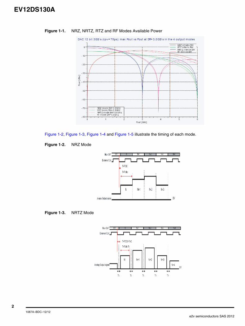
The component has been designed with a number of different operating modes as described below.Optimum performance can be obtained by choosing the correct mode depending on the particular bandof use.
Output modes:
Beside the classical NRZ modes EV12DS130A MUXDAC offers 3 other innovative output modes toenhance performance over 1st, 2nd or 3rd Nyquist zones.
• Narrow RTZ with optimal performance over 1st and beginning of 2nd Nyquist Zones.
• RTZ mode: to take advantage of a ½ sinc(X/2) roll off where X is normalized output frequency for optimal operation over 2nd Nyquist Zone.
• RF mode: for optimum available power beyond beginning of 2nd Nyquist zone.
The figure below shows the response against frequency for the different modes.
Visit our website: www.e2v.comfor the latest version of the datasheet
e2v semiconductors SAS 2012 1087A–BDC–12/12
EV12DS130A
Figure 1-1. NRZ, NRTZ, RTZ and RF Modes Available Power
Figure 1-2, Figure 1-3, Figure 1-4 and Figure 1-5 illustrate the timing of each mode.
Figure 1-2. NRZ Mode
Figure 1-3. NRTZ Mode
21087A–BDC–12/12
e2v semiconductors SAS 2012
EV12DS130A
Figure 1-4. RTZ Mode
Figure 1-5. RF Mode
As a general rule:
NRZ mode offers max power for 1st Nyquist operation and also best performance in the lower frequen-cies up to 200 MHz – 300 MHz. It also removes the parasitic spur at the clock frequency (in differential).
• RTZ mode offers slow roll off for 2nd Nyquist or 3rd Nyquist operation
• RF mode offers maximum power over 2nd and 3rd Nyquist operation
• NRTZ mode offers optimum power over full 1st and first half of 2nd Nyquist zones. This is the most relevant in term of performance for operation over 1st and beginning of 2nd Nyquist zone, depending on the sampling rate the zero of transmission moves in the 3rd Nyquist zone from begin to end when sampling rate increases.
31087A–BDC–12/12
e2v semiconductors SAS 2012

EV12DS130A
OCDS Mode
The OCDS bits control the DSP clock frequency according to the table below.
The timing diagram for a 1:4 DMUX is shown below.
Figure 1-6. OCDS Timing Diagram for 4:1 MUX
Normally for systems using a single DAC and FPGA, OCDS = 00 would be used. This would remove theneed for a multiplication of the DSP clock within the FPGA. (The data should always be supplied to theEV12DS130A at the sample rate (DDR)).
However for systems with multiple EV12DS130As and FPGAs, a slower DSP clock might be usefulsince it could be used to synchronise each FPGA output more easily since there would not be the poten-tial for timing ambiguities due to skew which could be the case with a fast DSP clock.
In these cases a multiplication of the clock is required in the FPGA.
Table 1-1. OCDS[1:0] Coding Table
Label Value Description
OCDS [1:0]
00 DSP clock frequency is equal to the sampling clock divided by 2N
01 DSP clock frequency is equal to the sampling clock divided by 2N*2
10 DSP clock frequency is equal to the sampling clock divided by 2N*4
11 DSP clock frequency is equal to the sampling clock divided by 2N*8
External CLK
Internal CLK/4 is used to clock the Data input A, B, C, D into EV12DS130A DAC
Internal CLK/4
DSP clock is internal CLK/4 divided by OCDS selection. This clock could be used as DDR clock for the FPGA
DSP with OCDS[00]
DSP with OCDS[01]
DSP with OCDS[10]
DSP with OCDS[11]
41087A–BDC–12/12
e2v semiconductors SAS 2012

EV12DS130A
IUCM Mode(Function only available for part numbers in ceramic package. Current part numbers areEV12DS130AGS, EV12DS130AMGSD/T, EV12DS130AMGS9NB1. Check with e2v for other partnumbers)
The Input Under Clocking mode (IUCM) is used the enable users who have access to only a limited inputdata rate. In this mode the input data rate is reduced by a factor of 2 while still keeping the DAC samplingrate at its required value (up to 3 GSps).
This is done by reducing the DSP clock to half the nominal rate, given DMUX and OCDS settings.
The effect of this is that the usable bandwidth, the width of the Nyquist zones, is reduced by a factor oftwo. This is because the effective input sampling rate is reduced by 2.
Also the position of the null frequency for each response curve is reduced.
Figure 1-7. Response Curves for IUCM = 1
However it can be seen by comparing the curves in IUCM and non-IUCM modes that, particularly at highfrequencies, there is very little power loss in the response of the EV12DS130A.
51087A–BDC–12/12
e2v semiconductors SAS 2012

EV12DS130A
Figure 1-8. Response Curves Non IUCM Mode
Use of PSS and HTVF, STVF
PSS is used to adjust the timing of the DSP clock so that the reception of the data by the EV12DS130Ais optimum. A typical connection scheme is shown below.
Figure 1-9. Typical Connection Scheme for FPGA and EV12DS130A
The signal IDC should have the same timing as the data signals.
STVL will be high if a set-up time violation is detected by the EV12DS130A and HVTL will be high if holdtime violation is detected. In this way the FPGA can monitor these signals and adjust its own phasedelay circuits or make an adjustment to the PSS value in the EV12DS130A.
FPGA DAC
IDC
Port A
Port B
Port C
Port D
HTVF, STVF
OCDS
2
2
24
24
24
24
2
2
DSP
3PSS
CLKDIV2
τ
OUT2
61087A–BDC–12/12
e2v semiconductors SAS 2012
EV12DS130A
Note that a divider circuit is necessary for these signals to ensure that the correct voltage levels aremaintained for interface with FPGA.
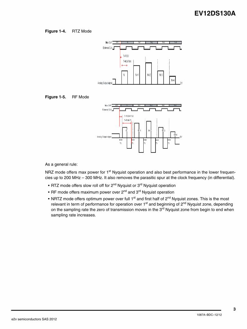
STVL/ HTVL Operation
IDC is sampled by 3 latches driven by 3 different clock separated by half a period of the master clock(3 GHz clock),
The central clock being the one used to latch datas. If the output of the said 3 latches are different the isa set up or an hold time issue depending on the latch which is different from the central latch.
Transitions on both edges of IDC are detected.
The master clock is the undivided external 3 GHz clock after buffering for edge sharpening...
Figure 1-10. Block Diagram of Circuit
Figure 1-11. Timing Diagram
71087A–BDC–12/12
e2v semiconductors SAS 2012

EV12DS130A
The flags STVF and HTVF have a risetime of the order of 100ns, see Figure 1-12 below.
Figure 1-12. STVF, HTVF Risetime
This means that these flags will not capture any 'one shot' timing error but need to be used as part of asystem that sets up the timing on initialization and then detects long term drifts in timing value.
The procedure recommended is to sweep the input data (along with IDC) delay over the input capturerange. This can be done by varying the PSS value. The point at which either of the STVF and HTVFflags goes high should be recorded. The final PSS timing value should be placed away from this errortiming zone.
Note that the Flags will repeat over a cycle of input data ( 4 clock cycles for Demux 4:1) so for examplethe flags are active at PSS = 7 the optimum timing position will be PSS = 3 or 4.
2. EV12DS130A Circuit Design Analogue Output (OUT/OUTN)
The analogue output should be used in differential fashion as described in the figures below.
If the application requires a single-ended analogue output, then a balun is necessary to generate a sin-gle-ended signal from the differential output of the DAC.
Figure 2-1. Analogue Output Differential Termination
MUXDACVCCA
100 nF
100 nFOUT
OUTN
Current Switches
AGND
50Ω
50Ω
50Ω lines
OUT
OUTN
AGND
81087A–BDC–12/12
e2v semiconductors SAS 2012

EV12DS130A
Figure 2-2. Analogue Output using a 1/ν2 a Balun
Note: The AC coupling capacitors should be chosen as broadband capacitors with a value depending on the application.
Clock Input (CLK/CLKN)
The DAC input clock (sampling clock) should be entered in differential mode as described in Figure 2-3.
Figure 2-3. Clock Input Differential Termination
Note: The buffer is internally pre-polarized to 2.5V (buffer between VCC5 and AGND).
MUXDAC
AGND
50Ω
50Ω lineOUT
50Ω line
1/sqrt
50Ω line
100 nF
100 nFOUT
OUTN
VCCA
Current Switches
50Ω
AGND
Differential sinewave 50Ω
Source
CLK
CLKN
DAC Clock Input Buffer
50Ω
50Ω
AGND
3.75 pF
C = 100 pF
C = 100 pF
2.5V
50Ω line
50Ω line
50Ω line
50Ω line
91087A–BDC–12/12
e2v semiconductors SAS 2012

EV12DS130A
Figure 2-4. Clock Input Differential with Balun
Note: The AC coupling capacitors should be chosen as broadband capacitors with a value depending on the application.
Digital Data, SYNC and IDC Inputs
LVDS buffers are used for the digital input data, the reset signal (active low) and IDC signal.
They are all internally terminated by 2 x 50 to ground via a 3.75 pF capacitor.
Figure 2-5. Digital Data, Reset and IDC Input Differential Termination
Notes: 1. In the case when only two ports are used (2:1 MUX ratio), then the unused data should be left open (no connect).
2. Data and IDC signals should be routed on board with the same layout rules and the same length.
Single sinewave 50Ω
Source
CLK
CLKN
DAC Clock Input Buffer
50Ω
50Ω
AGND
C = 100 pF
C = 100 pF
2.5 V
50Ω line
50Ω line
50Ω line
1/sqrt2
LVDS Output Buffer
In
InN
DAC Data and Sync Input Buffer
50Ω
50Ω
DGND
3.75 pF
50Ω line
50Ω line
101087A–BDC–12/12
e2v semiconductors SAS 2012

EV12DS130A
DSP Clock
The DSP, DSPN output clock signals are LVDS compatible.
They have to be terminated via a differential 100Ω termination as described in Figure 2-5.
Figure 2-6. DSP Output Differential Termination
Control Signal Settings
The MUX, MODE, PSS and OCDS control signals use the same static input buffer.
Logic "1" = 30 KΩ to Ground, or tied to VCCD = 3.3V or left open
Logic "0" = 10Ω to Ground or Grounded
Figure 2-7. Control Signal Settings
The control signal could be driven by FPGA.
Figure 2-8. Control Signal Settings with FPGA
Logic "1" > VIH or VCCD = 3.3V
Logic "0" < VIL or 0V
DAC Output DSP
Differential Output buffers
Z0 = 50Ω
Z0 = 50Ω
100Ω Termination
DSP
DSPN
To Load
10Ω 30 KΩ
GND GND
Control Signal Pin
Control Signal Pin
Control Signal Pin
Not Connected
Active Low Level (‘0’) Inactive High Level (‘1’)
Control Signal PinFPGA
111087A–BDC–12/12
e2v semiconductors SAS 2012

EV12DS130A
HTVF and STVF Control signal
The HTVF and STVF control signals is a output 3.3V CMOS buffer.
These signals could be acquired by FPGA.
Figure 2-9. Control Signal Settings with FPGA
Note: Due to limitations of Volmax of these signals a potential divider is required to meet minimum input values at FPGAs from some manufacturers.
GA Function Signal
This function allows you to adjust the internal gain of the DAC
The gain of the DAC can be tuned with applied analog voltage from 0 to VCCA3
This analog input signal could be generated by a DAC controlled by FPGA or microcontroller or a resis-tor network could be used. It should be ensured that the signal is stable enough for the applicationrequirements.
Figure 2-10. Control Signal Settings with GA
Power supplies decoupling and bypassing
The DAC requires 3 distinct power supplies:
VCCA5 = 5V (for the analogue core)
VCCA3 = 3.3V (for the analogue part)
VCCD = 3.3V (for the digital part)
It is recommended to decouple all power supplies to ground as close as possible to the device balls with100 pF in parallel to 10 nF capacitors. The minimum number of decoupling pairs of capacitors can becalculated as the minimum number of groups of neighboring pins.
4 pairs of 100 pF in parallel to 10 nF capacitors are required for the decoupling of VCCA5.4 pairs for the VCCA3 is the minimum required and finally, 10 pairs are necessary for VCCD.
FPGASVTL,HVTL10K
4K7
GADAC16bFPGAn
121087A–BDC–12/12
e2v semiconductors SAS 2012

EV12DS130A
Figure 2-11. Power Supplies Decoupling Scheme
Each power supply has to be bypassed as close as possible to its source or access by 100 nF in parallelto 22 µF capacitors (value depending of DC/DC regulators).
Board Layout
It is recommended that layout guidelines described in the application note 0999B - 'Design Consider-ations for Mixed signal PCB layout' should be followed.
In addition with regard to PCB track tolerance it is recommended that the tracking tolerance for digitalinputs is: - between differential pairs is ± 2.5 mm and between each pair a tolerance of ±1 mm.
For analog outputs and Clock inputs the tolerance is recommended at ±0.1mm between each line of thedifferential pair.
Power Sequence
For best performance the power supplies should be sequenced in the following order.
1st power supply: VCCD = 3.3V
2sd power supply: VCCA3 = 3.3V
3rd power supply: VCCA5 = 5V
Synchronisation Procedure
The SYNC signal can be applied to the component to reset the timing block circuit. This is for use whenmultiple DACs are used and the output timing of each one needs to be synchronised. After the applica-tion of the SYNC signal the DSP clock from the EV12DS130A will stop for a period and after a constantand known time the DSP clock will start up again.
Depending on the settings for OCDS and also the MUX ratio the width of the SYNC pulse must begreater than a certain number of external clock pulses. It is also necessary that the sync pulse should bean integer number of clock pulses.
DAC 12-bit
VBCCD B
VBCcA5
VBCCA3B
AGND
AGND
DGND
100 pF
10 nF
100 pF
10 nF
100 pF
10 nF
X 4 (min)
X 2 (min)
X 4 (min)
131087A–BDC–12/12
e2v semiconductors SAS 2012

EV12DS130A
The SYNC pulse should be synchronous with the external clock, there is also a forbidden zone in rela-tion to the SYNC and clock signals which causes a metastable response. The timings below should notbe used (Figure 2-14).
To correctly perform the synchronisation procedure the SYNC pulse should be synchronised with thefalling edge of the clock.
Figure 2-12. Sync Timing 2:1 MUX
The diagram below shows the signals expected during a correct operation of SYNC.
Figure 2-13. Correct Sync Signals
Table 2-1. OCDS Values and SYNC Minimum Pulse Widths
SYNC min width
MUX 4 :1 MUX 2 :1
OCDS0 3 Clk cycles 1 Clk cycle
OCDS1 5 Clk cycles 1 Clk cycle
OCDS2 13 Clk cycles 5 Clk cycles
OCDS3 32 clk cycles 13 Clk cycles
Pipeline + output delay
SYNC pulse length
. T
SYNC
DSP Clock
3 GHz
RESET DSPDSP clk
SYNC
Master clock : Fc
141087A–BDC–12/12
e2v semiconductors SAS 2012
EV12DS130A
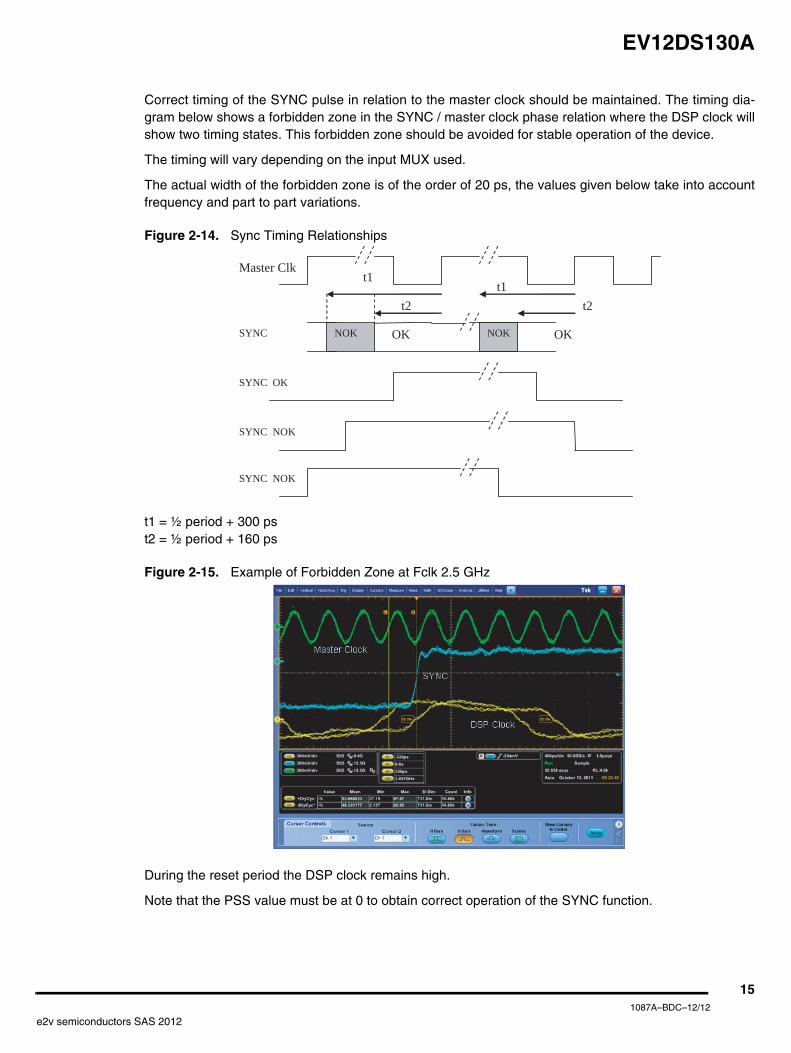
Correct timing of the SYNC pulse in relation to the master clock should be maintained. The timing dia-gram below shows a forbidden zone in the SYNC / master clock phase relation where the DSP clock willshow two timing states. This forbidden zone should be avoided for stable operation of the device.
The timing will vary depending on the input MUX used.
The actual width of the forbidden zone is of the order of 20 ps, the values given below take into accountfrequency and part to part variations.
Figure 2-14. Sync Timing Relationships
t1 = ½ period + 300 pst2 = ½ period + 160 ps
Figure 2-15. Example of Forbidden Zone at Fclk 2.5 GHz
During the reset period the DSP clock remains high.
Note that the PSS value must be at 0 to obtain correct operation of the SYNC function.
SYNC OK OKNOK NOK
t1
t2
SYNC OK
SYNC NOK
SYNC NOK
Master Clk
t2t1
151087A–BDC–12/12
e2v semiconductors SAS 2012

EV12DS130A
PSS may not be needed in systems using more recent FPGAs since the delay mechanism can be incor-porated in the I/O pad.
If use of PSS is required the reset procedure to be followed should be:
Store value of PSSSet PSS = 0Re-sync SystemReset PSS value.
Choice of Balun
The choice of balun is very important, the use of a non-optimised balun can produce larger thanexpected harmonics.
Figure 2-16 on page 16 below illustrates the dramatic degradations induced by an inappropriate Balunchoice (part of the band of interest out of the specified domain of the Balun).
The following figure illustrates the possible improvement when using a more appropriate Balun.
The measurements are performed in RTZ mode, for a –3dBFS tone generated at the same frequenciesfor Fclock and Fout, with different Baluns to perform de Diff to single conversion before spectrumanalyzer.
The following graph shows spectrum in 1st Nyquist zone with balun "KRYTAR" in mode RTZ.
Figure 2-16. Spectrum of 1st Nyquist Zone using Krytar Balun
H2 and H4 are much higher because bandwidth of "balun" in is not adapted. We note also one rise ofnoise floor in band DC to 450 MHz.
H2
H3
Fondamental : 1482MHz
H4
Balun :KRYTAR (0.5G – 7G)
Balun out of band
161087A–BDC–12/12
e2v semiconductors SAS 2012
EV12DS130A
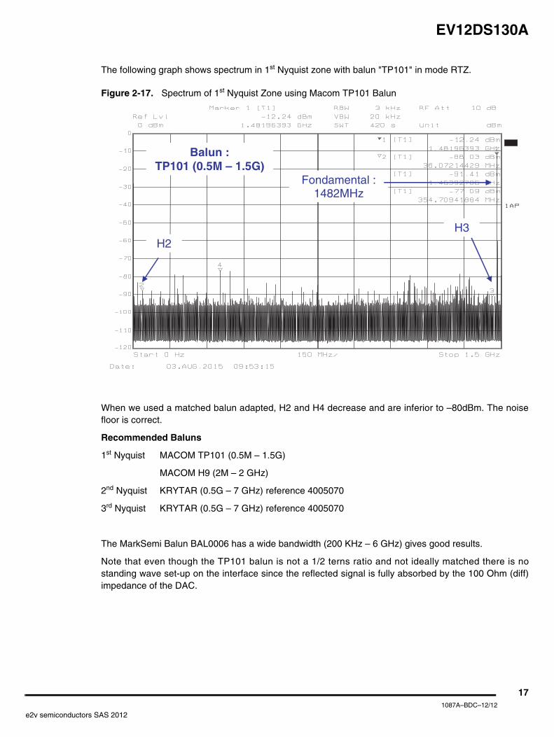
The following graph shows spectrum in 1st Nyquist zone with balun "TP101" in mode RTZ.
Figure 2-17. Spectrum of 1st Nyquist Zone using Macom TP101 Balun
When we used a matched balun adapted, H2 and H4 decrease and are inferior to –80dBm. The noisefloor is correct.
Recommended Baluns
1st Nyquist MACOM TP101 (0.5M – 1.5G)
MACOM H9 (2M – 2 GHz)
2nd Nyquist KRYTAR (0.5G – 7 GHz) reference 4005070
3rd Nyquist KRYTAR (0.5G – 7 GHz) reference 4005070
The MarkSemi Balun BAL0006 has a wide bandwidth (200 KHz – 6 GHz) gives good results.
Note that even though the TP101 balun is not a 1/2 terns ratio and not ideally matched there is nostanding wave set-up on the interface since the reflected signal is fully absorbed by the 100 Ohm (diff)impedance of the DAC.
H2H3
Fondamental : 1482MHz
Balun :TP101 (0.5M – 1.5G)
171087A–BDC–12/12
e2v semiconductors SAS 2012

EV12DS130A
Output Capacitors
If the EV12DS130A is used to generate microwave frequencies, it is recommended to use a high fre-quency capacitor (example below) as the output DC block to the system.
181087A–BDC–12/12
e2v semiconductors SAS 2012

EV12DS130A
Improving NPR and ACPR
This note is regarding a feature of the EV12DS130A and EV10DS130A.The NPR and ACPR performance of these devices can be improved by the use of the proceduredescribed in this document.
This family of DACs use an internal band-gap voltage reference for regulating the output voltage, if thisband-gap is not set-up correctly there is an impact on its noise behaviour. This will be seen in a reducedNPR or ACPR performance.It does not pay a large effect in the single tone harmonic performance of the device.With an Fclk of 3 GHz we have seen an improvement of 2 – 3 dB in NPR with the band-gap in the correctstate.At Fclk 1.5 GHz the effect is more marked and with the band-gap correctly set we see an NPR of around55 dB, if it is not set we see an NPR of around 48 dB.
The graph below shows the performance differences:It can be seen that without the correct setting band-gap setting the NPR value remains at around46 – 47 dB no matter what the Fclk frequency.
However with the band-gap correctly set the NPR performance at lower Fclk values improvessignificantly.
Figure 2-18. NPR variation with and without correct bandgap setting
The incorrectly set-up band-gap has an increased noise profile which is flat over the values of Fclk.
The correctly set-up band-gap has a much lower noise power and hence as Fclk is reduced it is normalthat the noise power due to the DAC reduces. However when the band-gap is not correctly set-up thenoise from this dominates the over-all noise performance.
191087A–BDC–12/12
e2v semiconductors SAS 2012
EV12DS130A
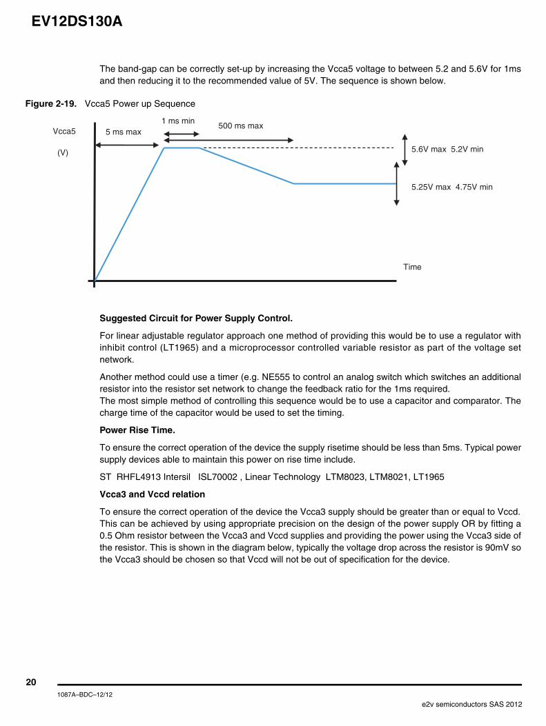
The band-gap can be correctly set-up by increasing the Vcca5 voltage to between 5.2 and 5.6V for 1msand then reducing it to the recommended value of 5V. The sequence is shown below.
Figure 2-19. Vcca5 Power up Sequence
Suggested Circuit for Power Supply Control.
For linear adjustable regulator approach one method of providing this would be to use a regulator withinhibit control (LT1965) and a microprocessor controlled variable resistor as part of the voltage setnetwork.
Another method could use a timer (e.g. NE555 to control an analog switch which switches an additionalresistor into the resistor set network to change the feedback ratio for the 1ms required.The most simple method of controlling this sequence would be to use a capacitor and comparator. Thecharge time of the capacitor would be used to set the timing.
Power Rise Time.
To ensure the correct operation of the device the supply risetime should be less than 5ms. Typical powersupply devices able to maintain this power on rise time include.
ST RHFL4913 Intersil ISL70002 , Linear Technology LTM8023, LTM8021, LT1965
Vcca3 and Vccd relation
To ensure the correct operation of the device the Vcca3 supply should be greater than or equal to Vccd.This can be achieved by using appropriate precision on the design of the power supply OR by fitting a0.5 Ohm resistor between the Vcca3 and Vccd supplies and providing the power using the Vcca3 side ofthe resistor. This is shown in the diagram below, typically the voltage drop across the resistor is 90mV sothe Vcca3 should be chosen so that Vccd will not be out of specification for the device.
1 ms min5 ms max
5.6V max 5.2V min
5.25V max 4.75V min
500 ms max
Time
Vcca5
(V)
201087A–BDC–12/12
e2v semiconductors SAS 2012

EV12DS130A
Figure 2-20. Schematic of Power Supply arrangement with Vccd and Vcca linked by 0.5Ohhm
This also has the advantage of reducing the number of required power supplies for the system.
To ensure that this approach did not limit the performance of the device a number of tests were per-formed on a system having the recommended decoupling as described above.
The results are shown below.
Figure 2-21. Test Results of schematic in Figure 2-20 on page 21
REF = Data of part with separated supply voltages.
SFDR results also showed no overall loss in performance.
DAC 12 bit
VCCA5
VCCDB
VCCA3B B
DGND
AGND
AGND
100 pF
10 nF
100 pF
10 nF
100 pF
10 nF
X 4 (min)
X 2 (min)
X 4 (min)
3V3
0.5 Ohm
211087A–BDC–12/12
e2v semiconductors SAS 2012

1087A–BDC–12/12e2v semiconductors SAS 2012
Notice:
Whilst e2v has taken care to ensure the accuracy of the information contained herein it accepts no responsibility for the consequences of any use thereofand also reserves the right to change the specification of goods without notice. e2v accepts no liability beyond that set out in its standard conditions of salein respect of infringement of third party patents arising from the use of tubes or other devices in accordance with information contained herein.Users of e2v products are responsible for their own products and applications.e2v technologies does not assumes liability for application support and assistance.e2v technologies reserves the right to modify, make corrections, improvements and other changes to its products and services at any time andto discontinue any product without notice. Customers are advised to obtain the latest relevant information prior to placing orders and should ver-ify that such information is current and complete.
How to reach usHome page: www.e2v.com
Sales offices:
Europe Regional sales office
e2v ltd
106 Waterhouse Lane
Chelmsford Essex CM1 2QU
England
Tel: +44 (0)1245 493493
Fax: +44 (0)1245 492492
mailto: [email protected]
e2v sas
16 Burospace
F-91572 Bièvres Cedex
France
Tel: +33 (0) 16019 5500
Fax: +33 (0) 16019 5529
mailto: [email protected]
e2v Aerospace and defense inc
765 Sycamore Drive
Milpitas
California 95035
USA
Tel: +33 (0) 1 408 737 0992
Fax: +33 (0) 1 408 736 8708
mailto: e2v-us.com
Americas
e2v inc
520 White Plains Road
Suite 450 Tarrytown, NY 10591
USA
Tel: +1 (914) 592 6050 or 1-800-342-5338,
Fax: +1 (914) 592-5148
mailto: [email protected]
Asia Pacific
e2v ltd
11/F.,
Onfem Tower,
29 Wyndham Street,
Central, Hong Kong
Tel: +852 3679 364 8/9
Fax: +852 3583 1084
mailto: [email protected]
Product Contact:
e2v
Avenue de Rochepleine
BP 123 - 38521 Saint-Egrève Cedex
France
Tel: +33 (0)4 76 58 30 00
Hotline:
mailto: [email protected]