datasheet - teledyne-e2v.com · sd /mmc sp i 2x du ar t 4x i2c clocks /reset gpio ccs r bootr om 2x...
TRANSCRIPT

P2041QorIQ Integrated Processor
Hardware SpecificationsDatasheet DS1103
Datasheet
Whilst Teledyne e2v Semiconductors SAS has taken care to ensure the accuracy of the information contained herein it accepts no responsibility for theconsequences of any use thereof and also reserves the right to change the specification of goods without notice. Teledyne e2v Semiconductors SAS accepts noliability beyond the set out in its standard conditions of sale in respect of infringement of third party patents arising from the use of the devices in accordance withinformation contained herein.
Teledyne e2v Semiconductors SAS, avenue de Rochepleine 38120 Saint-Egrève, France Holding Company: Teledyne e2v Semiconductors SAS
Telephone: +33 (0)4 76 58 30 00
MAIN FEATURESThe P2041 QorIQ integrated communication processorcombines four Power Architecture® processor cores withhigh performance data path acceleration logic and networkand peripheral bus interfaces required for power intensiveapplications in aerospace, defence and demandingoutdoor environments.
This device can be used for combined control, data path,and application layer processing. Its high level of integra-tion offers significant performance benefits compared tomultiple discrete devices, while also greatly simplifyingboard design.
This chip includes the following functions and features:
• Four e500mc Power Architecture Cores, Each with a Backside 128 KB L2 Cache with ECC
– Three Levels of Instructions: User, Supervisor, and Hypervisor
– Independent Boot and Reset – Secure Boot Capability
• CoreNet Fabric Supporting Coherent and non-coherent Transactions Amongst CoreNet Endpoints
• One 1 MB CoreNet Platform Cache with ECC • CoreNet Bridges Between the CoreNet Fabric the I/Os,
Data Path Accelerators, and High and Low Speed Peripheral Interfaces
• One 10-Gigabit Ethernet (XAUI) Controller
• Five 1-Gigabit Ethernet Controllers – 2.5 Gbps SGMII Interfaces – RGMII Interfaces
• One 64-bit DDR3 and DDR3L SDRAM Memory Controller with ECC
• Multicore Programmable Interrupt Controller • Four I2C Controllers • Four 2-pin UARTs or two 4-pin UARTs • Two 4-channel DMA Engines • Enhanced Local Bus Controller (eLBC) • Three PCI Express 2.0 Controllers/Ports • Two Serial RapidIO® Controllers/ports (sRIO Port)
Supporting Version 1.3 with Features 2.1 • Two Serial ATA (SATA 2.0) Controllers • Enhanced Secure Digital Host Controller (SD/MMC) • Enhanced Serial Peripheral Interface (eSPI) • 2× High-speed USB 2.0 Controllers with Integrated
PHYs
Teledyne e2v Semiconductors SAS 2018
Contact Teledyne e2v by e-mail: [email protected] or visit www.teledyne-e2v.com for global sales and operations centres
1103D–HIREL–06/18

P2041
Figure 0-1. Block Diagram
1. Pin Assignments and Reset States This section provides a top view of the Ball layout diagram and four detailed views by quadrant. It alsoprovides a pinout listing by bus.
1.1 780 FC-PBGA Ball Layout Diagrams These figures show the FC-PBGA ball map diagrams.
Pe rfMonitor
CoreNetTr ac e
Wa tchpointCro ss
Tr igger
Real Time De bug
Aurora
10-Lane 5-GHz SerDe s
sRIO
1.3
/2.
11GE
1GE
128-Kb yteBacksideL2 Cache
10GE
Fr ame Manager
1GE
PCIe
2.0
PCIe
2.0
PCIe
2.0
2x DM A
P2041Po wer Ar chitecture®
e500mc Core
RapidI ORMan
Secu rity4. 2
Pa tternMatchEngine
2.1
eLB CQueue
Mgr
Bu fferMgr
eOpenPIC
Internal
Po wer Mgmt
SD /MMC
SP I
2x DU AR T
4x I2C
Clocks /Reset
GPIO
CCS R
BootR OM
2xUSB 2.0 PH Y
Secur ityMonitor
PreBootLoader
32-K byteD-Cache
32-K byteI-Cache
1024-Kb yteFr ontside
Cor eNet Platf orm
64-bitDDR3/DDR3 L
Memor y Controller
CoreNet ™Coherency F abric
PA MU PA MUPA MU PA MUPe ripheral
Access Mgmt Unit
Bu ffer
Pa rs e, Classify ,Distribute
SATA
2.0
sRIO
1.3
/2.1
1GE
1GE
SATA
2.0
Cache
21103D–HIREL–06/18
Teledyne e2v Semiconductors SAS 2018

P2041
Figure 1-1. 780 BGA Ball Map Diagram (Top View)
[19]VDD_
A
B
C
D
E
F
G
H
J
K
L
M
N
P
1
SGND[12]
AVDD_SRDS1
SVDD[04]
SD_RX[03]
SGND[02]
SD_RX[02]
SVDD[01]
LGPL[5]
LGPL[1]
LAD[04]
LDP[1]
LAD[09]
LBCTL
2SD_RX[04]
SVDD[11]
AGND_SRDS2
SGND[05]
SD_RX[03]
SVDD[02]
SD_RX[02]
SGND[01]
GND[143]
LAD[02]
LGPL[4]
GND[121]
LAD[07]
LA[20]
3
SD_RX[04]
SVDD[10]
SGND[06]
SD_REF_CLK1
SGND[03]
SD_TX[03]
XGND[02]
GND[152]
LGPL[3]
LA[17]
LDP[0]
LWE[1]
LAD[08]
LA[19]
4
SVDD[17]
SD_TX[04]
XVDD[12]
SD_REFCLK1
SVDD[03]
SD_TX[03]
XVDD[02]
GND[151]
LAD[01]
LAD[03]
BVDD[5]
LCLK[0]
BVDD[2]
LAD[10]
BVDD[1]
LAD[12]
5 6 7 8 9 10
SGND SVDDSD_
SGNDSD_ SVDD
[17] [16] RX [16] RX [15][05] [06]
SD_SGND
SD_ SVDDSD_ SGND
TX [11]RX
[09]RX [10]
[04] [05] [06]
XGND NC XGND SD_ XVDDSD_
[12] [35] [11] TX[11]
TX[05] [06]
NC NC XVDDSD_
XGND SD_
[33] [32] [08]TX [07] TX[05] [06]
SEE DETAIL A NC NC NC NCRSRV RSRV[30] [29] [28] [27]
SD_XVDD XGND IMP_NC NC NC
[03] [04] CAL_RX [17] [16] [15]
SD_ SD_ SEN VDD_TX TX
NCSEGND_ CA_PL
GND
[02] [02] [07] CA_PL [78][159]
SEN VDD_XGND XVDD NCSEVDD_ CA_PL
GND[01] [01] [06] CA_PL [150]
[72]
LAD LAD BVDD GNDVDD_ GND
[05] [00] [7] [142] CA_PL [141][66]
GND LAD BVDD GNDVDD_ GND
[135] [16] [6] [134] CA_PL [133][60]
LGPL LGPL BVDD GNDVDD_ GND
[0] [2] [4] [127] CA_PL [126][54]
GND LWE BVDD GNDVDD_ GND
[120] [0] [3] [119] CA_PL [118][48]
LAD GNDVDD_ GND
LALE LCLK[113] CA_PL [112][06] [1] [42]
GND LA LCS GNDVDD_ GND
[105] [18] [1] [104] CA_PL [103][36]
LCS LA LAD GNDVDD_ GND
[0] [24] [11] [096] CA_PL [095][30]
LA LAD LAD GND VDD_ GND[25] [14] [15] [087] CA_PL [086]
11 12 13 14 15 16 17 18SD_ SD_ SD_ SGND AVDD_ SVDDRX SGND RX SVDD RX [14] SRDS2 [13][07] [15] [10] [14] [11]
SD_ SD_ SD_ SVDD AGND_ SGNDSVDD SGNDRX RX RX[07] SRDS2 [08][07] [14] [10] [09]
[11]
XGND SD_ XVDDSD_
XGND SD_ SVDDSD_
TX TX TX TX[10][07] [10] [10] [09]
[11] [05] [12]
SD_ SD_XVDD XGND XVDDSD_
SGND SD_
[07] TX TX TX [04] TX[07]
[06] [10] [06] [11] [12]
SD_NC NC NC NC NC NC NC[26] [25] [24] [23] [22] [21] REF_ [20]
CLK2
SD_NC NC NC NC NCRSRV RSRV[14] [13] [12] [11] REF_ [10]
CLK2
VDD_ GNDVDD_ GND
VDD_ GNDVDD_ GND
CA_PL [158] CA_PL [157] CA_PL [156] CA_PL [155][77] [76] [75] [74]
VDD_ GNDVDD_ GNDVDD_ GND
VDD_ GNDCA_PL [147] CA_PL [146]CA_PL [149] CA_PL [148]
[69] [68][71] [70]VDD_ GND
VDD_ GND VDD_ GNDVDD_ GND
CA_PL [140] CA_PL [139] CA_PL [138] CA_PL [137][65] [64] [63] [62]
VDD_ GNDVDD_ GND VDD_ GND
VDD_ GNDCA_PL [132] CA_PL [131] CA_PL [130] CA_PL [129]
[59] [58] [57] [56]VDD_ GND VDD_ GND
VDD_ GNDVDD_ GND
CA_PL [125] CA_PL [124] CA_PL [123] CA_PL [122][53] [52] [51] [50]
VDD_ GND VDD_ GND VDD_ GNDVDD_ GND
CA_PL [117] CA_PL [116] CA_PL [115] CA_PL [114][47] [46] [45] [44]
VDD_ GND VDD_ GND VDD_ GNDVDD_ GND
CA_PL [111] CA_PL [110] CA_PL [109] CA_PL [108][41] [40] [39] [38]
VDD_ GND VDD_ GNDVDD_ GND
VDD_ GNDCA_PL [102] CA_PL [101] CA_PL [100] CA_PL [099]
[35] [34] [33] [32]
VDD_ GND VDD_ GND VDD_ GNDVDD_ GND
CA_PL [094] CA_PL [093] CA_PL [092] CA_PL [091][29] [28] [27] [26]
VDD_ GND VDD_ GND VDD_ GNDVDD_ GND
CA_PL [085] CA_PL [084] CA_PL [083] CA_PL [082][23] [22] [21] [20]
VDD_VDD_ VDD_
19 20 21 22 23 24
SD_ SD_ EC1_SGND SVDD GND GTX_RX
[13]RX [12] [168]
[12] [13] CLK125
SD_ SD_ EC1_RX
SVDD RXSGND GND TX_
[12] [06] [13][07] [167] D0
XVDDSD_ XGND NC GND
EC1_
[09] TX [08] [34] [165]RX_
[13] CLK
SD_ EC2_XGND XVDD NC GND
[05] TX [05] [31] [164]GTX_
[13] CLK125SEE DETAIL B NC NC SD_ XVDD EMI2_ GND[19] [18] IMP_ MDIO [162]CAL_TX [04]
NC NC XGND GND EMI1_ EMI2[09] [08] [03] [161] MDC MDC
VDD_ LVDD GND GND SPI_ EMI1_CA_PL [3] [154] [153] MISO MDIO
[73]VDD_ LVDD GND SPI_ SPI_ SPI_CA_PL [2] [145] CLK CS1 CS3
[67]VDD_ GND USB2_CA_PL
LVDD USB2_ VDD_ USB2_
[61][1] [136] AGND6 3P3 AGND5
VDD_ CVDD GND USB2_CA_PL [128] VDD_ RSRV RSRV
[55][2] 1P0
VDD_ LP_ USB1_CA_PL VDD_LP TMP_ VDD_ RSRV RSRV
[49] DETECT 1P0
VDD_ CVDD NC USB1_ USB1_ USB1_CA_PL AGND3 VDD_ AGND2[1] [M21] 3P3[43]VDD_ OVDD GND SDHC_ SDHC_ SDHC_CA_PL [6] [107] CMD DAT CLK
[37] [0]
VDD_ GND USB_
25 26 27 28EC1_
EC1_ EC1_RX_ ADV TXD3 RXD1
GND EC1_ EC1_ EC1_ B[166] RXD3 RXD2 RXD0
EC1_ LVDDEC1_
EC1_TX_ CTXD1 [5] EN TXD2
EC2_ EC1_RX_ GTX_ GND EC2_ DDV CLK [163] RXD3
EC2_ EC2_EC2_
LVDD[4] RXD2 ERXD1 GTX_CLK
EC2_ EC2_ EC2_RX_ RX_ GND TX_ FCLK D0 [160]
EN
EC2_ EC2_ EC2_ EC2_TX_ TX_ TX_ TX_ GD0 D2 D1 D3
GND SPI_ SPI_ SPI_ H[144] CS0 CS3 MISI
USB2_VBUS_ USB2_ USB2_ USB2_ JCLMP
AGND4 UID AGND6
USB2_ USB2_ USB1_ USB1_ KAGND3 UDP AGND5 UDP
USB2_ USB2_ USB1_ USB1_ LAGND2 UDM AGND4 UDM
USB1_ USB2_ USB1_ USB1_VBUS_ AGND1 UID AGND1 MCLMP
GND SDHC_ SDHC_ SDHC_DAT DAT DAT N[106][1] [2] [3]
OVDD UART2_ UART1_ UART2_ UART2_ UART2_CA_PL [5] [098] CLKIN CTS RTS RTS SOUT SIN
RTC P[31]
VDD_ OVDD GND ASLEEP UART1_ GND UART1_ UART1_ GND SYSCLK RCA_PL [4] [090] SOUT [089] CTS SIN [088][25]
VDD_ OVDD GND TMP_ CKSTP_ OVDD CLK_ TEST_
R LCS[3]
GND[097]
LA[21]
TLA[22]
LA[27]
LA[26]
ULA[23]
LAD[13]
LA[29]
V LA[30]
GND[071]
LA[31]
W NC[05]
GND[058]
NC[04]
Y MDQ[04]
MDM[0]
MDQ[05]
AA MDQS[0]
MDQS[0]
MDQ[06]
AB MDQ[02]
GND[032]
MDQ[03]
AC MDQ[24]
MDQ[25]
MDQ[28]
AD MDQS[3]
MDQS[3]
MDQS[1]
AE MDQ[30]
GND[019]
MDQ[31]
AF MDQ[26]
MDQ[27]
MECC[1]
AG MECC[4]
MECC[5]
MDQS[8]
AH MECC[0]
MDQS[8]
1 2 3
Signal Gr oups
CA_PL [3] [081]PORESETHRESET DETECT OUT [2] OUT SEL T
GND EVT EVT RESET_ U[072] [2] [1] REQ
IRQ EVT GND SCAN_ V[04] [0] [059] MODE
IIC2_ OVDD TMS TDI WSCL [1]
IIRQ_ IIRQ_ TRST TCK Y[00] [06]
IIC2_ IIRQ_ GND TDO AASDA [03] [033]
IIRQ_ IIC3_ IIRQ_ IO_VSEL AB
IIC1_ GND IIRQ_ IIC1_ ACSCL [022] [09] SDA
MDQ MDQ MDQ MDQ
[02] SDA [0][0]
AD
MDQ MDM GND MDQS AE
[58] [59] [62] [63]
[55] [7] [011] [7]
MDQ MDQ MDQ MDQS[61] [56] [57] [7] AF
GND MDQ MDQ MDQ AG[003] [47] [43] [60]
MDM MDQ MDQ AH[5] [46] [42]
25 26 27 28
[24]
LA TEMP_ GND GNDVDD_ GNDSEE DETAIL C LCS2 [28] CATHODE [080] [079] CA_PL[18]
[078]
GND[070]
TEMP_ANODE
GND[069]
AVDD_CC1
GND[068]
VDD_CA_PL
[13]
GND[067]
NC[03]
GND[057]
AVDD_DDR MVREF GND
[056]
VDD_CA_PL
[09]
GND[055]
MDQ[00]
MDQ[01]
GND[048]
GND[047]
GND[046]
VDD_CA_PL
[05]
GND[045]
MDQ GND MDQ GND GVDD GVDD GVDD[07] [038] [12] [037] [17] [16] [15]
MDQ[13]
MDQ[08
MDQ[09]
MCKE[1]
MCKE[0]
GND[031]
GND[030]
MDQ[29]
GND[025]
MDQ[14]
MDM[1]
MBA[2]
MA[12]
MA[07]
MDQS[1]
MDM[3]
MDQ[15]
MDQ[21]
MDM[2]
MDQS[2]
MDQ[22]
MDQ[10]
GND[018]
MDQ[11]
MDQ[20]
GND[017]
MDQS[2]
MDQ[23]
MDM[8]
MECC[7]
GVDD[05]
MDQ[16]
MDQ[17]
GVDD[04]
MA[08]
GND MECC MCKE GND MA MA GND[008] [2] [3] [007] [14] [11] [006]
MECC MECC MCKE MA MAPAR MA MA[6] [5] [2] [15] _ERR [09] [05]
4 5 6 7 8 9 10
GND GND VDD_CB GND VDD_CBCA_PL [077] CA_PL [076] CA_PL [11] [075] [10]
[15]VDD_ GND VDD_ GND
[17] [16]VDD_ GND GND VDD_CB
CA_PL [066] CA_PL [065] CA_PL [064] [063] [09][10]
VDD_ GND VDD_ GND
[12] [11]VDD_ VDD_CB GND VDD_CBCA_PLCA_PL [054] CA_PL [053][06] [07] [052] [06]
[08] [07]VDD_ GND VDD_ GND
VDD_ GND GND VDD_CBCA_PL [042] [041] [04]CA_PL [044] CA_PL [043]
[02]
GVDD GVDD GVDD GVDD
[04] [03]
GVDD SENSE GND VDD_CB[10] GND_CB [036] [02][14] [13] [12] [11]
GND SENSEGND GND GVDD GVDD RSRV RSRV[027] VDD_CB[029] [028] [09] [08]
MA MA GVDD GVDD MBA MBA GND MCS[1] [0] [024] [0][06] [02] [07] [06]
GND MDQ MDQS MDQSMDQ GND MCK MCK[020] [33] [4] [4][18] [021] [1] [0]
GND MDQ MDM GNDGND MDIC MCK MCK[016] [1] [1] [0] [015] [32] [4] [014]
MDQ MDQ GVDD MDQMDQ MA GND GND[36] [37] [03] [38][19] [01] [010] [009]
MA MDIC MCK MCK MAPAR MA MCS MODT[04] [0] [2] [3] _OUT [00] [2] [2]
GND MAMA GND MCK MCK[03] [002] [2] [3] [001] [10] MRAS MWE
11 12 13 14 15 16 17 18
AVDD_OVDD I/O Supply Voltage SVDD SerDes Core Power Supply SRDS1 SerDes 1 PLL Supply Voltage VDD_CA Core Group A Voltage Sense
AVDD_ SENSE-LVDD I/O Supply Voltage XVDD SerDes Transcvr Pad Supply SRDS2 SerDes 2 PLL Supply Voltage VDD_CB Core Group B Voltage Sense
VDD_ AVDD_GVDD DDR DRAM I/O Supply CA_PL Core Group A & Platform Supply PLAT Platform PLL Supply Voltage RSRV ReservedVoltage
CVDD SPI Voltage Supply VDD_ AVDD_ Core PLL Supply Voltage POVDD Fuse Programming Override SupplyCore Group B Supply Voltage CCCB
SENSE-BVDD Local Bus I/O Supply VDD_CA_CB_PLCore A, B and Platform Voltage Sense
GNDCA_PL POVDD GND IO_ EVT
[074] [ 073] VSEL1 [4][14]
GND VDD_CB GND AVDD_ GND IIC4_[062] [08] [061] PLAT [060] SDA
GND VDD_CB GND AVDD_ GND EVTSEE DETAIL D [051] [05] [050] CC2 [049] [3]
GND VDD_CB IO_ GND IO_IRQ
[040] [03] VSEL_ [039] VSEL_
GND VDD_CB CA_PL IIRQ_ IIRQ_ GND
[4] [3] OUT
VDD_
[035] [01] [01] [05] [07] [034]
IO_ GND IIC3_ IIRQ_RSRV RSRV VSEL [026] SCL [10][2]
MODT GND IIRQ_ IIC4_ IIRQ_[0] [023]
MCS1[08] SCL [11]
MDQ MDQ MDQ MODT MDQ MDQ[35] [53] [49] [1] [54] [51]
MDQ MDQ GND MDQS MDQS GND[34] [52] [013] [6] [6] [012]
MDQ GVDD MDQ MDM GVDD MDQ[39] [02] [48] [6] [01] [50]
GND MCS MDQ GND MDQ MDQS[005] [3] [44] [004] [41] [5]
MA MODT MDQ MDQ MDQSMCAS [13] [3] [45] [40] [5]
19 20 21 22 23 24
SENSE-
31103D–HIREL–06/18
Teledyne e2v Semiconductors SAS 2018

P2041
Figure 1-2. 780 BGA Ball Map Diagram (Detail View A)
RSRV
RSRVRSRV
LA[18]
GND[102]
GND[101]
GND[103]
VDD_CA_PL
[36]
VDD_CA_PL
[35]
VDD_CA_PL
[34]
GND[104]
LCS[1]
LAD[10]
LA[20]
LA[19]
GND[111]
GND[110]
GND[112]
VDD_CA_PL
[42]
VDD_CA_PL
[41]
VDD_CA_PL
GND[113]
LCLKLALELAD[06]
LAD[07]
GND[117]
GND[116]
GND[118]
VDD_CA_PL
[48]
VDD_CA_PL
[47]
VDD_CA_PL
[46]
GND[120]
LCLK[0]
LBCTL
LAD[09]
LDP[1]
GND[127]
GND[119]
BVDD[4]
LGPL[2]
LGPL[0]
BVDD[5]
LDP[0]
LGPL[4]
LAD[04]
VDD_CA_PL
[58]
VDD_CA_PL
[59]
VDD_CA_PL
[60]
GND[132]
GND[133]
GND[134]
GND[131]
LAD[16]
GND[135]
LAD[03]
LA[17]
LAD[02]
LGPL[1]
VDD_CA_PL
[64]
VDD_CA_PL
[65]
VDD_CA_PL
[66]
GND[140]
GND[141]
BVDD[6]
BVDD[7]
LAD[00]
LAD[05]
LAD[01]
GND[148]
VDD_CA_PL
[70]
VDD_CA_PL
[72]
SENSEVDD_CA_PL
XVDD[01]
NC[06]
SGND[01]
SVDD[01]
GND[157]
VDD_CA_PL
[77]
SENSEGND_CA_PL
NC[07]
SD_TX[02]
SD_TX[02]
XVDD[02]
XGND[02]
SD_RX[02]
SD_RX[02]
NC[13]
NC[12]
NC[15]
NC[14]
NC[17]
NC[16]
SD_IMP_
CAL_RX
XGND[04]
XVDD[03]
SD_TX[03]
SD_TX[03]
SVDD[02]
SGND[02]
NC[24]
NC[23]
NC[26]
NC[25]
NC[28]
NC[27]
NC[30]
NC[29]
SVDD[03]
SGND[03]
SD_RX[03]
SD_RX[03]
XVDD[07]
XGND[07]
SD_TX[10]
SD_TX[07]
SD_TX[06]
SD_TX[05]
XVDD[08]
SD_REFCLK1
SD_REF_CLK1
NC[33]
SGND[05]
SVDD[04]
SD_TX[10]
SD_TX[07]
SD_TX[06]
SD_TX[05]
XGND[10]
XVDD[10]
XVDD[11]
AGND_SRDS2
AVDD_SRDS1
SGND[09]
SD_RX[10]
SD_RX[07]
SD_RX[06]
SD_RX[05]
SD_TX[04]
SVDD[10]
SVDD[11]
SGND[11]
SGND[12]
SD_RX[04]
SD_RX[04]
SGND[17]
SD_RX[05]
SGND[16]
SD_RX[06]
SD_RX[10]
XGND[12]
SGND[06]
SVDD[09]
XGND[06]
VDD_CA_PL GND
[158]
GND[151]
GND[150]
GND[143]
GND[142]
GND[125]
GND[124]
GND[121]
BVDD[3]
BVDD[2]
GND[105]
SD_RX[07]
SGND[15]
SVDD[17]
SVDD[16]
SVDD[15] [14]
SVDD
SGND[10] [14]
SVDD
XVDD[12]
XGND[11]
NC[35]
NC[32]
SD_TX[04]
[78]
GND[159]
VDD_CA_PL
[76]
GND[152]
XGND[01]
VDD_CA_PL
[71]
GND[149]
LGPL[5]
LGPL[3]
GND[139]
GND[126]
VDD_CA_PL
[54]
VDD_CA_PL
[53]
VDD_CA_PL
[52]
LWE[1]
LWE[0]
LAD[08] [1] [40]
1 1312111098765432
A
B
C
D
E
F
G
H
J
K
L
M
N
14
P
41103D–HIREL–06/18
Teledyne e2v Semiconductors SAS 2018

P2041
Figure 1-3. 780 BGA Ball Map Diagram (Detail View B)
RSRV
RSRVRSRV
RSRVRSRV
UART2_SOUT
RTCUART2_SIN
UART2_RTS
UART1_RTS
UART2_CTS
USB_CLKIN
OVDD[5]
GND[100]
GND[099]
VDD_CA_PL
[33]
VDD_CA_PL
[32]
VDD_CA_PL
SDHC_DAT[3]
SDHC_CLK
SDHC_DAT[2]
SDHC_DAT[1]
GND[106]
OVDD[6]
GND[109]
GND[108]
VDD_CA_PL
[39]
VDD_CA_PL
[38]
VDD_CA_PL
[37]
USB1_AGND1
USB1_UID
USB2_AGND1
USB1_VDD_3P3
CVDD[1]
GND[115]
GND[114]
VDD_CA_PL
[45]
VDD_CA_PL
[44]
VDD_CA_PL
USB1_UDM
USB1_AGND4
USB2_UDM
USB1_VDD_1P0
USB2_AGND2
CVDD[2]
USB1_UDP
USB1_AGND5
USB2_UDP
GND[128]
GND[129]
GND[130]
VDD_CA_PL
[55]
VDD_CA_PL
[56]
VDD_CA_PL
[57]
USB2_AGND6
USB2_UID
USB2_AGND4
USB2_VBUS_USB2_
AGND5 CLMP
USB2_VDD_USB2_
AGND6GND[137]
GND[138]
VDD_CA_PL
[61]
VDD_CA_PL
[62]
VDD_CA_PL
[63]
LVDD[1]
SPI_MISI
SPI_CS3
SPI_CS0
SPI_CS3
SPI_CLK
GND[144]
GND[145]
GND[146]
GND[147]
VDD_CA_PL
[67]
VDD_CA_PL
[68]
VDD_CA_PL
[69]
EC2_TX_D3
EC2_TX_D1
EC2_TX_D2
EC2_TX_D0
EMI1_MDIO
LVDD[3]
GND[153]
GND[155]
GND[156]
VDD_CA_PL
[74]
EMI1_MDC
EC2_RX_CLK
EC2_TX_EN
GND[161]
XGND[03]
NC[08]
NC[09]
EC2_GND[162]
SD_IMP_
CAL_TX
SD_REF_CLK2
NC[18]
NC[19]
NC[22]
EC2_RXD3
EC1_GTX_CLK
EC2_RX_DV
EC2_GTX_
CLK125
GND[163]
GND[164]
NC[31]
XVDD[05]
SD_TX[13]
XGND[05]
SD_TX[12]
SGND[04]
SD_TX[11]
XVDD[06]
LVDD[5]
EC1_TX_EN
EC1_TXD2
EC1_TXD1
EC1_RX_CLK
GND[165]
NC[34]
XGND[08]
SD_TX[12][05]
SVDDSD_TX[11]
XGND[09]
EC1_RXD0
EC1_RXD2
EC1_RXD3
GND[166]
EC1_TX_D0
SD_RX[13][06]
SVDDSD_RX[12]
AGND_SRDS2[07]
SVDDSD_RX[11]
SGND[08]
EC1_TXD3
EC1_RX_DV
EC1_GTX_
CLK125
SGND[14]
AVDD_SRDS2
NC[21]
NC[20]
NC[11]
NC[10]
GND[123]
GND[122]
GND[154]
GND[168]
XVDD[04]
GND[160]
GND[136]
VDD_LP
GND[107]
GND[098]
EC2_
SD_RX[11] [13]
SVDDSD_RX[12]
SVDD[12]
EC1_RXD1
SGND[07]
GND[167]
XVDD[09]
SD_TX[13]
SD_REF_CLK2
EC2_RX_D0
VDD_CA_PL
[75]
VDD_CA_PL
[73]
SPI_MISO
LVDD[2]
3P3
USB2_VDD_1P0
USB2_AGND3
VDD_CA_PL
[51]
VDD_CA_PL
[50]
VDD_CA_PL
[49]
LP_TMP_
DETECT
[43]
USB1_AGND3
USB1_AGND2
USB1_VBUS_CLMP
SDHC_CMD
SDHC_DAT[0]
[31]
SPI_CS1
NC[M21]
EMI2MDC
EMI2_MDIO
SGND[13]
19 24 25 26 27 2815 16 17 18
A
B
C
D
E
F
G
H
J
K
L
M
N
2322
P
2120
RXD2 LVDD[4] EC2_RXD2
GTX_CLK
SD_RX[13]
51103D–HIREL–06/18
Teledyne e2v Semiconductors SAS 2018

P2041
Figure 1-4. 780 BGA Ball Map Diagram (Detail View C)
MCK[2]
MCK[3]
GND[002]
MA[05]
MA[09]
MAPAR_ERR
MA[15]
MA[03]
MECC[5]
MECC[6]
MDQS[8]
MECC[0]
MA[04]
MCK[2]
MDIC[0]
MCK[3]
GND[006]
MA[11]
MA[14]
GND[007]
MCKE[3]
MECC[2]
MDQS[8]
MECC[4]
MECC[5]
GND[009]
MA[01]
MDQ[19]
MA[08]
GVDD[04]
MDQ[26]
MDQ[27]
MDM[8]
MECC[1]
MECC[7]
MCK[0]
MDIC[1]
MCK[1]
GND[016]
MDQ[23]
MDQS[2]
GND[017]
MDQ[20]
MDQ[11]
GND[018]
MDQ[10]
MDQ[31]
GND[019]
MDQ[30]
MCK[0]
MDQ[15]
MDQS[2]
MDQ[21]
MDM[2]
MDQS[3]
MDQS[1]
MDQS[3]
MDQS[1]
GVDD[06]
GVDD[07]
MA[02]
MA[06]
GVDD[08]
GVDD[09]
GND[028]
GND[030]
GND[031]
MDQ[13]
MDQ[03]
GND[032]
MDQ[02]
GVDD[11]
GVDD[12]
GVDD[13]
GVDD[14]
GVDD[15]
GVDD[16]
GVDD[17]
GND[037]
GND[038]
GND[044]
GND[043]
GND[045]
VDD_CA_PL
[05]
VDD_CA_PL
[04]
VDD_CA_PL
[03]
GND[046]
GND[047]
MDQ[04]
MDQ[00]
MDM[0]
MDQ[05]
GND[054]
GND[053]
GND[055]
VDD_CA_PL
[09]
VDD_CA_PL
[08]
VDD_CA_PL
[07]
GND[056]MVREFAVDD_
DDRGND[057]
NC[03]
NC[04]
GND[058]
NC[05]
GND[066]
GND[065]
GND[067]
VDD_CA_PL
[13]
VDD_CA_PL
[12]
VDD_CA_PL
[11]
AVDD_CC1
GND[070]
LA[31]
GND[071]
LA[30]
GND[077]
GND[076]
GND[078]
VDD_CA_PL
[18]
VDD_CA_PL
[17]
VDD_CA_PL
[16]
GND[079]
GND[080]
TEMP_CATHODE
GND[085]
GND[084]
GND[086]
VDD_CA_PL
[24]
VDD_CA_PL
[23]
VDD_CA_PL
[22]
GND[087]
LAD[15]
LA[25]
LAD[14]
LAD[12]
LA[27]
LA[26]
GND[094]
GND[093]
GND[095]
VDD_CA_PL
[30]
VDD_CA_PL
[29]
VDD_CA_PL
[28]
LAD[11]
LA[24]
LCS[0]
GND[097]
GND[096]
GND[068]
MDQ[14]
MDM[1]
MDQ[22]
MDQ[17]
MCKE[2]
GND[048]
GND[029]
MA[12]
GND[021]
GND[010]
GND[008]
MDQ[08
MDQ[09]
MDM[3]
MDQ[16]
LCS[3]
LA[21]
BVDD[1]
LA[22]
LA[28]LCS2
LAD[13]
LA[29]
LA[23]
TEMP_ANODE
GND[069]
MDQ[01]
MDQS[0]
MDQ[07]
MDQS[0]
MDQ[06]
MDQ[12]
MCKE[1]
MCKE[0]
GND[025]
MDQ[24]
MDQ[29]
MDQ[25]
MDQ[28]
MBA[2]
MA[07]
MDQ[18]
MCK[1]
GVDD[05]
GND[054]
GND[053]
GND[055]
VDD_CA_PL
[09]
VDD_CA_PL
[08]
VDD_CA_PL
[07]
GND[066]
GND[065]
GND[067]
VDD_CA_PL
[13]
VDD_CA_PL
[12]
VDD_CA_PL
[11]
1 1312111098765432
AH
AG
AF
AE
AD
AA
14
AC
AB
Y
W
U
V
T
R
61103D–HIREL–06/18
Teledyne e2v Semiconductors SAS 2018

P2041
Figure 1-5. 780 BGA Ball Map Diagram (Detail View D)
MDQ[45]
MA[13]
MODT[3]MRAS
MA[10]
MDQ[40]
MDQS[5]
MDM[5]
MDQ[46]
GND[001]
MDQ[47]
MDQ[43]
GND[003]
MDQ[41]
MDQS[5]
GND[004]
MCS[3]
MDQ[44]
GND[005]
MAPAR_OUT
MCS[2]
MA[00]
MODT[2]
MDQ[50]
MDQ[61]
MDQ[56]
MDQ[57]
MDQS[7]
GVDD[01]
MDM[6]
MDQ[48]
GVDD[02]
MDQ[39]
MDQ[38]
GVDD[03]
MDQ[37]
MDQ[36]
MDQS[7]
MDQ[55]
MDM[7]
GND[012]
MDQS[6]
MDQS[6]
GND[013]
MDQ[34]
MDQ[52]
GND[014]
MDQ[32]
MDM[4]
GND[015]
MDQ[49]
MDQ[51]
MODT[1]
MDQ[54]
MDQ[33]
MDQ[35]
MDQS[4]
MDQS[4]
MDQ[58]
MDQ[53]
MDQ[59]
IIC1_SDA
IIRQ_[09]
IIC1_SCL
IIRQ_[11]
IIC4_SCL
IIRQ_[08]
MCS1MCS[0]
MODT[0]
MBA[0]
MBA[1]
IIC3_SDA
IIRQ_[02]
IIC3_SCL
GND[026]
IO_VSELRSRV
SENSEVDD_CB
IIC2_SDA
IIRQ_[07]
IIRQ_[05]
SENSEGND_CB
GVDD[10]
TRST TCKIIRQ_[06]
IIRQ_[00]
IRQOUT
IO_VSEL_
[3]
TDIOVDD
[1]IIC2_SCL
VDD_CA_PL
[06]
SCAN_MODE
EVT[0]
IRQ[04]
IIC4_SDA
AVDD_CC2
VDD_CA_PL
[10]
RESET_REQ
EVT[1]
EVT[4]
IO_VSEL1
TEST_TMP_ OVDD[2]
HRESETPORESETGND[083]
GND[082]
VDD_CA_PL
[21]
VDD_CA_PL
[20]
VDD_CA_PL
[19]
OVDD[3]
SYSCLKGND[088]
UART1_SIN
UART1_SOUT
GND[090]
GND[092]
GND[091]
VDD_CA_PL
[27]
VDD_CA_PL
[26]
VDD_CA_PL
[25]
OVDD[4]
VDD_CB[11]
GND[063]
VDD_CB[09]
GND[049]
GND[040]
GND[039]
VDD_CB[03]
VDD_CB[02]
GND[035]
VDD_CB[01]
GND[034]
GND[033]
GND[023]
GND[022]
GND[011]
GND[089]
GND[081]
GND[074]
GND[073]
GND[072]
GND[062]
GND[061]
GND[060]
VDD_CB[08]
GND[059]
GND[042]
GND[041]
VDD_CB[04]
GND[027]
GND[024]
GND[020]
ASLEEP UART1_CTS
DETECTCKSTP_
OUT
VDD_CA_PL
[15]
GND[075]
VDD_CB[10]
VDD_CA_PL
[14]POVDD EVT
[2]
CLK_OUT
GND[064]
AVDD_PLAT
VDD_CB[07]
GND[052]
VDD_CB[06]
GND[051]
GND[050]
VDD_CB[05]
EVT[3]
TMS
VDD_CA_PL
[02]
IO_VSEL_
[4]
GND[036]
VDD_CA_PL
[01]TDOIIRQ_
[03]
[2]
IIRQ_[10]
IIRQ_[0]
IO_VSEL
[0]
MDQ[62]
MDQ[63]
MDQ[60]
MWE MCAS MDQ[42]
RSRV RSRV RSRV
19 24 25 26 27 28
AH
AG
AF
AE
AD
AA
2322
AC
AB
Y
W
2120
U
V
T
R
15 181716
SEL
71103D–HIREL–06/18
Teledyne e2v Semiconductors SAS 2018

P2041
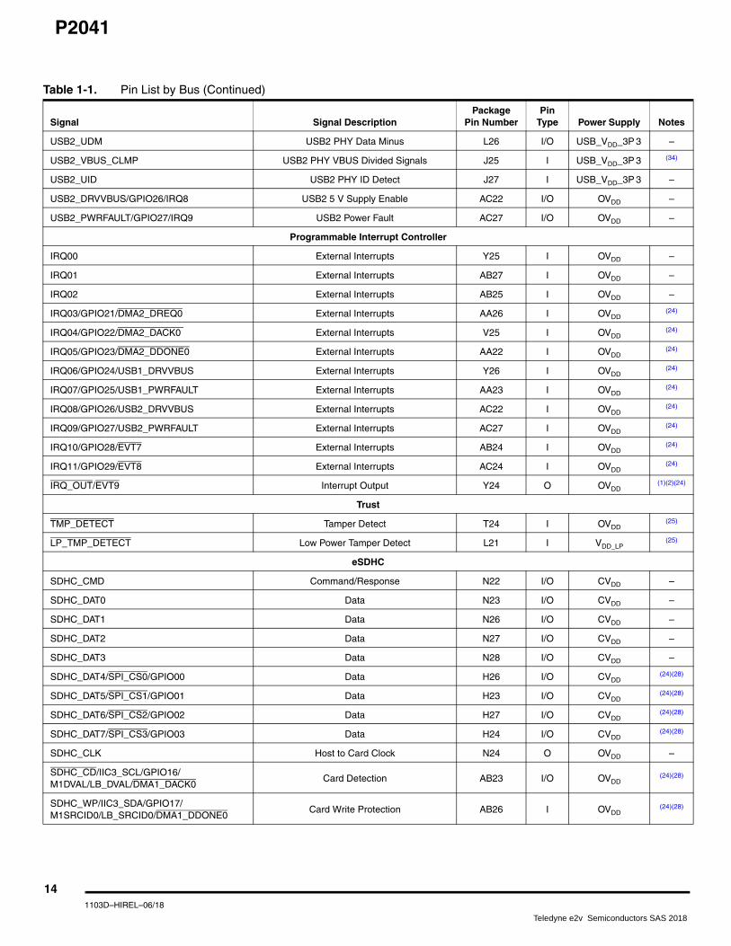
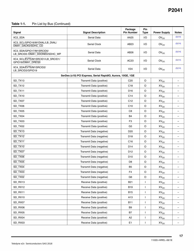
1.2 Pinout List This table provides the pinout listing for the 780 FC-PBGA package by bus. Pins for multiplexed signalsappear in the bus group for their default status and have a corresponding note stating that they havemultiple functionality depending on the mode in which they are configured.
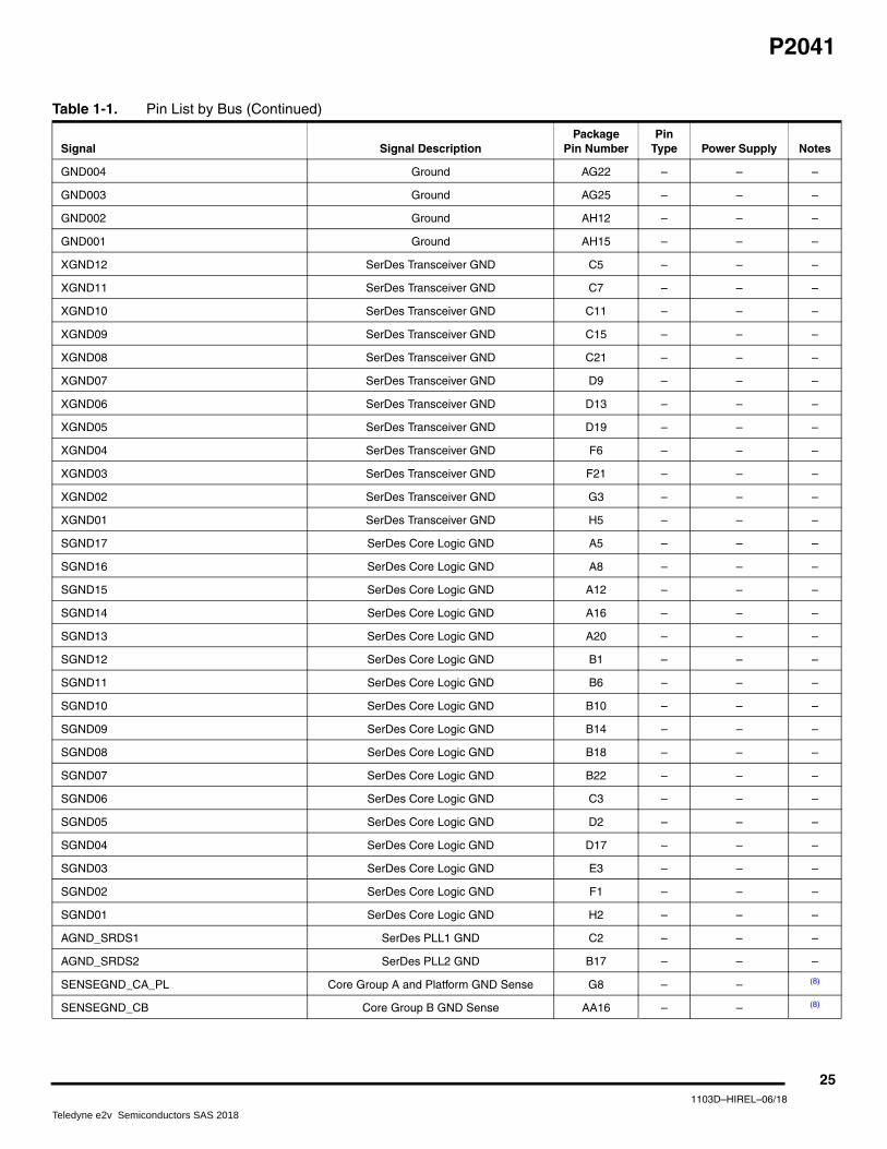
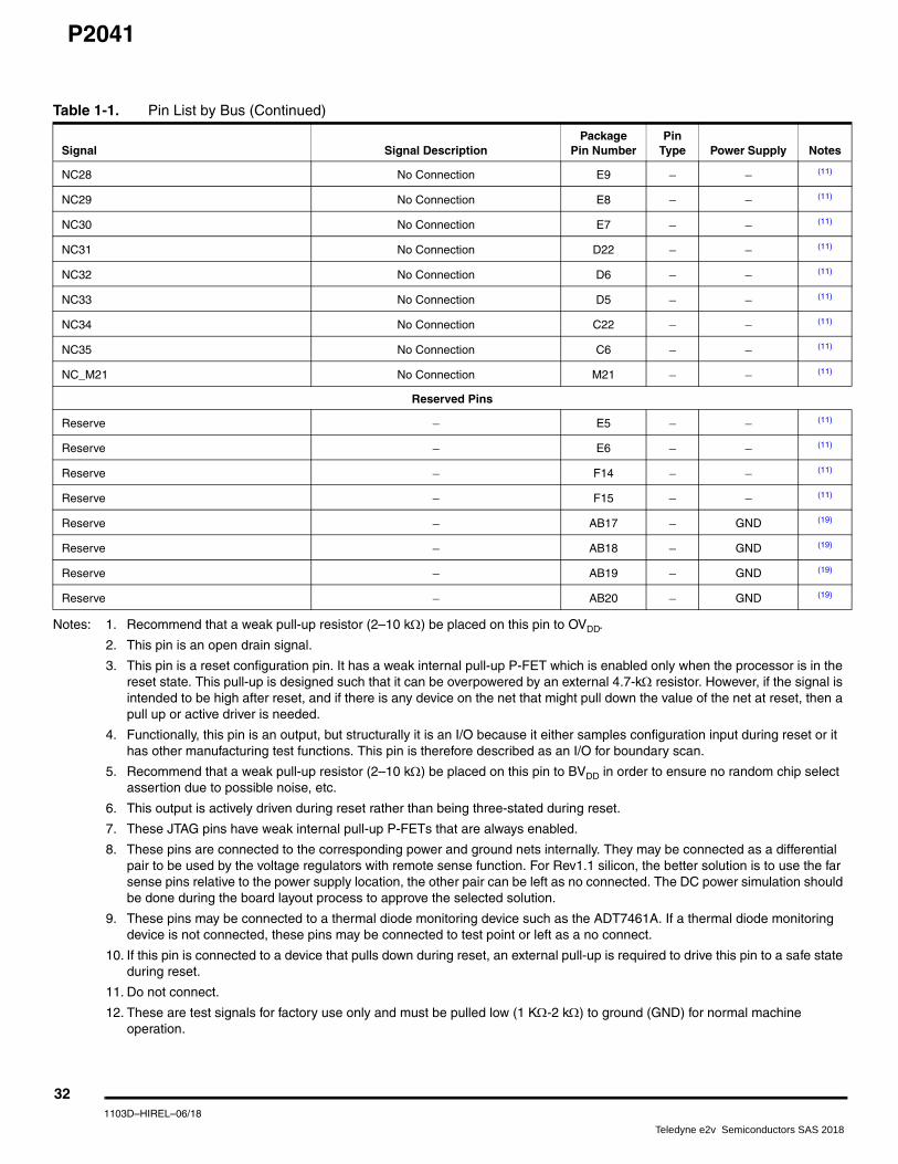
Table 1-1. Pin List by Bus
Signal Signal Description Package
Pin NumberPin
Type Power Supply Notes
DDR SDRAM Memory Interface
MDQ00 Data Y4 I/O GVDD –
MDQ01 Data Y5 I/O GVDD –
MDQ02 Data AB1 I/O GVDD –
MDQ03 Data AB3 I/O GVDD –
MDQ04 Data Y1 I/O GVDD –
MDQ05 Data Y3 I/O GVDD –
MDQ06 Data AA3 I/O GVDD –
MDQ07 Data AA4 I/O GVDD –
MDQ08 Data AB5 I/O GVDD –
MDQ09 Data AB6 I/O GVDD –
MDQ10 Data AE4 I/O GVDD –
MDQ11 Data AE6 I/O GVDD –
MDQ12 Data AA6 I/O GVDD –
MDQ13 Data AB4 I/O GVDD –
MDQ14 Data AC6 I/O GVDD –
MDQ15 Data AD6 I/O GVDD –
MDQ16 Data AF7 I/O GVDD –
MDQ17 Data AF8 I/O GVDD –
MDQ18 Data AD11 I/O GVDD –
MDQ19 Data AF11 I/O GVDD –
MDQ20 Data AE7 I/O GVDD –
MDQ21 Data AD7 I/O GVDD –
MDQ22 Data AD10 I/O GVDD –
MDQ23 Data AE10 I/O GVDD –
MDQ24 Data AC1 I/O GVDD –
MDQ25 Data AC2 I/O GVDD –
MDQ26 Data AF1 I/O GVDD –
MDQ27 Data AF2 I/O GVDD –
MDQ28 Data AC3 I/O GVDD –
MDQ29 Data AC4 I/O GVDD –
MDQ30 Data AE1 I/O GVDD –
MDQ31 Data AE3 I/O GVDD –
81103D–HIREL–06/18
Teledyne e2v Semiconductors SAS 2018

P2041
MDQ32 Data AE16 I/O GVDD –
MDQ33 Data AD16 I/O GVDD –
MDQ34 Data AE19 I/O GVDD –
MDQ35 Data AD19 I/O GVDD –
MDQ36 Data AF15 I/O GVDD –
MDQ37 Data AF16 I/O GVDD –
MDQ38 Data AF18 I/O GVDD –
MDQ39 Data AF19 I/O GVDD –
MDQ40 Data AH23 I/O GVDD –
MDQ41 Data AG23 I/O GVDD –
MDQ42 Data AH27 I/O GVDD –
MDQ43 Data AG27 I/O GVDD –
MDQ44 Data AG21 I/O GVDD –
MDQ45 Data AH22 I/O GVDD –
MDQ46 Data AH26 I/O GVDD –
MDQ47 Data AG26 I/O GVDD –
MDQ48 Data AF21 I/O GVDD –
MDQ49 Data AD21 I/O GVDD –
MDQ50 Data AF24 I/O GVDD –
MDQ51 Data AD24 I/O GVDD –
MDQ52 Data AE20 I/O GVDD –
MDQ53 Data AD20 I/O GVDD –
MDQ54 Data AD23 I/O GVDD –
MDQ55 Data AE25 I/O GVDD –
MDQ56 Data AF26 I/O GVDD –
MDQ57 Data AF27 I/O GVDD –
MDQ58 Data AD25 I/O GVDD –
MDQ59 Data AD26 I/O GVDD –
MDQ60 Data AG28 I/O GVDD –
MDQ61 Data AF25 I/O GVDD –
MDQ62 Data AD27 I/O GVDD –
MDQ63 Data AD28 I/O GVDD –
MECC0 Error Correcting Code AH2 I/O GVDD –
MECC1 Error Correcting Code AF3 I/O GVDD –
MECC2 Error Correcting Code AG5 I/O GVDD –
MECC3 Error Correcting Code AH5 I/O GVDD –
MECC4 Error Correcting Code AG1 I/O GVDD –
Table 1-1. Pin List by Bus (Continued)
Signal Signal Description Package
Pin NumberPin
Type Power Supply Notes
91103D–HIREL–06/18
Teledyne e2v Semiconductors SAS 2018

P2041
MECC5 Error Correcting Code AG2 I/O GVDD –
MECC6 Error Correcting Code AH4 I/O GVDD –
MECC7 Error Correcting Code AF5 I/O GVDD –
MAPAR_ERR Address Parity Error AH8 I GVDD (4)
MAPAR_OUT Address Parity Out AG15 O GVDD –
MDM0 Data Mask Y2 O GVDD –
MDM1 Data Mask AC7 O GVDD –
MDM2 Data Mask AD8 O GVDD –
MDM3 Data Mask AD5 O GVDD –
MDM4 Data Mask AE17 O GVDD –
MDM5 Data Mask AH25 O GVDD –
MDM6 Data Mask AF22 O GVDD –
MDM7 Data Mask AE26 O GVDD –
MDM8 Data Mask AF4 O GVDD –
MDQS0 Data Strobe AA2 I/O GVDD –
MDQS1 Data Strobe AD3 I/O GVDD –
MDQS2 Data Strobe AE9 I/O GVDD –
MDQS3 Data Strobe AD1 I/O GVDD –
MDQS4 Data Strobe AD18 I/O GVDD –
MDQS5 Data Strobe AG24 I/O GVDD –
MDQS6 Data Strobe AE23 I/O GVDD –
MDQS7 Data Strobe AE28 I/O GVDD –
MDQS8 Data Strobe AH3 I/O GVDD –
MDQS0 Data Strobe AA1 I/O GVDD –
MDQS1 Data Strobe AD4 I/O GVDD –
MDQS2 Data Strobe AD9 I/O GVDD –
MDQS3 Data Strobe AD2 I/O GVDD –
MDQS4 Data Strobe AD17 I/O GVDD –
MDQS5 Data Strobe AH24 I/O GVDD –
MDQS6 Data Strobe AE22 I/O GVDD –
MDQS7 Data Strobe AF28 I/O GVDD –
MDQS8 Data Strobe AG3 I/O GVDD –
MBA0 Bank Select AC16 O GVDD –
MBA1 Bank Select AC15 O GVDD –
MBA2 Bank Select AC8 O GVDD –
MA00 Address AG16 O GVDD –
MA01 Address AF12 O GVDD –
Table 1-1. Pin List by Bus (Continued)
Signal Signal Description Package
Pin NumberPin
Type Power Supply Notes
101103D–HIREL–06/18
Teledyne e2v Semiconductors SAS 2018

P2041
MA02 Address AC12 O GVDD –
MA03 Address AH11 O GVDD –
MA04 Address AG11 O GVDD –
MA05 Address AH10 O GVDD –
MA06 Address AC11 O GVDD –
MA07 Address AC10 O GVDD –
MA08 Address AF10 O GVDD –
MA09 Address AH9 O GVDD –
MA10 Address AH16 O GVDD –
MA11 Address AG9 O GVDD –
MA12 Address AC9 O GVDD –
MA13 Address AH20 O GVDD –
MA14 Address AG8 O GVDD –
MA15 Address AH7 O GVDD –
MWE Write Enable AH18 O GVDD –
MRAS Row Address Strobe AH17 O GVDD –
MCAS Column Address Strobe AH19 O GVDD –
MCS0 Chip Select AC18 O GVDD –
MCS1 Chip Select AC21 O GVDD –
MCS2 Chip Select AG17 O GVDD –
MCS3 Chip Select AG20 O GVDD –
MCKE0 Clock Enable AB8 O GVDD –
MCKE1 Clock Enable AB7 O GVDD –
MCKE2 Clock Enable AH6 O GVDD –
MCKE3 Clock Enable AG6 O GVDD –
MCK0 Clock AD14 O GVDD –
MCK1 Clock AE13 O GVDD –
MCK2 Clock AG13 O GVDD –
MCK3 Clock AG14 O GVDD –
MCK0 Clock Complements AE14 O GVDD –
MCK1 Clock Complements AD13 O GVDD –
MCK2 Clock Complements AH13 O GVDD –
MCK3 Clock Complements AH14 O GVDD –
MODT0 On Die Termination AC19 O GVDD –
MODT1 On Die Termination AD22 O GVDD –
MODT2 On Die Termination AG18 O GVDD –
MODT3 On Die Termination AH21 O GVDD –
Table 1-1. Pin List by Bus (Continued)
Signal Signal Description Package
Pin NumberPin
Type Power Supply Notes
111103D–HIREL–06/18
Teledyne e2v Semiconductors SAS 2018

P2041
MDIC0 Driver Impedance Calibration AG12 I/O GVDD (16)
MDIC1 Driver Impedance Calibration AE12 I/O GVDD (16)
Local Bus Controller Interface
LAD00 Muxed Data/Address J6 I/O BVDD (3)
LAD01 Muxed Data/Address J4 I/O BVDD (3)
LAD02 Muxed Data/Address K2 I/O BVDD (3)
LAD03 Muxed Data/Address K4 I/O BVDD (3)
LAD04 Muxed Data/Address L1 I/O BVDD (3)
LAD05 Muxed Data/Address J5 I/O BVDD (3)
LAD06 Muxed Data/Address N5 I/O BVDD (3)
LAD07 Muxed Data/Address N2 I/O BVDD (3)
LAD08 Muxed Data/Address N3 I/O BVDD (3)
LAD09 Muxed Data/Address N1 I/O BVDD (3)
LAD10 Muxed Data/Address P4 I/O BVDD (3)
LAD11 Muxed Data/Address R7 I/O BVDD (3)
LAD12 Muxed Data/Address T4 I/O BVDD (3)
LAD13 Muxed Data/Address U2 I/O BVDD (3)
LAD14 Muxed Data/Address T6 I/O BVDD (3)
LAD15 Muxed Data/Address T7 I/O BVDD (3)
LA16 Address K6 I/O BVDD (31)
LA17 Address K3 I/O BVDD (37)
LA18 Address P6 I/O BVDD (31)
LA19 Address P3 I/O BVDD (31)
LA20 Address P2 I/O BVDD (31)
LA21 Address R3 I/O BVDD (31)
LA22 Address T1 I/O BVDD (31)
LA23 Address U1 I/O BVDD (3)
LA24 Address R6 I/O BVDD (3)
LA25 Address T5 I/O BVDD (31)
LA26 Address T3 I/O BVDD (3)(29)
LA27 Address T2 O BVDD –
LA28 Address U5 I/O BVDD –
LA29 Address U3 I/O BVDD –
LA30 Address V1 I/O BVDD –
LA31 Address V3 I/O BVDD –
LDP0 Data Parity L3 I/O BVDD –
LDP1 Data Parity M1 I/O BVDD –
Table 1-1. Pin List by Bus (Continued)
Signal Signal Description Package
Pin NumberPin
Type Power Supply Notes
121103D–HIREL–06/18
Teledyne e2v Semiconductors SAS 2018

P2041
LCS0 Chip Selects R5 O BVDD (5)
LCS1 Chip Selects P7 O BVDD (5)
LCS2 Chip Selects U4 O BVDD (5)
LCS3 Chip Selects R1 O BVDD (5)
LWE0 Write Enable M6 O BVDD –
LWE1 Write Enable M3 O BVDD –
LBCTL Buffer Control P1 O BVDD –
LALE Address Latch Enable N6 I/O BVDD –
LGPL0/LFCLE UPM General Purpose Line 0/ LFCLE–FCM L5 O BVDD (3)(4)
LGPL1/LFALE UPM General Purpose Line 1/ LFALE–FCM K1 O BVDD (3)(4)
LGPL2/LOE/LFRE UPM General Purpose Line 2/
LOE_B–Output Enable L6 O BVDD (3)(4)
LGPL3/LFWP UPM General Purpose LIne 3/
LFWP_B–FCM J3 O BVDD (3)(4)
LGPL4/LGTA/LUPWAIT/LPBSE UPM General Purpose Line 4/
LGTA_B–FCM L2 I/O BVDD (36)
LGPL5 UPM General Purpose Line 5 / Amux J1 O BVDD (3)(4)
LCLK0 Local Bus Clock M4 O BVDD –
LCLK1 Local Bus Clock N7 O BVDD –
DMA
DMA1_DREQ0/IIC4_SCL/EVT5/M1SRCID 1/LB_SRCID1/GPIO18
DMA1 Channel 0 Request AC23 I OVDD (24)
DMA1_DACK0/IIC3_SCL/GPIO16/SDHC_ CD/M1DVAL/LB_DVAL
DMA1 Channel 0 Acknowledge AB23 O OVDD (2)(14)
DMA1_DDONE0/IIC3_SDA/GPIO17/M1SR CID0/LB_SRCID0/SDHC_WP
DMA1 Channel 0 Done AB26 O OVDD (2)(14)
DMA2_DREQ0/IRQ03/GPIO21 DMA2 Channel 0 Request AA26 I OVDD (24)
DMA2_DACK0/IRQ04/GPIO22 DMA2 Channel 0 Acknowledge V25 O OVDD (24)
DMA2_DDONE0/IRQ05/GPIO23 DMA2 Channel 0 Done AA22 O OVDD (24)
USB Host Port 1
USB1_UDP USB1 PHY Data Plus K28 I/O USB_VDD_3P 3 –
USB1_UDM USB1 PHY Data Minus L28 I/O USB_VDD_3P 3 –
USB1_VBUS_CLMP USB1 PHY VBUS Divided Signals M25 I USB_VDD_3P 3 (34)
USB1_UID USB1 PHY ID Detect M27 I USB_VDD_3P 3 –
USB_CLKIN USB PHY Clock Input P22 I OVDD –
USB1_DRVVBUS/GPIO24/IRQ6 USB1 5 V Supply Enable Y26 O OVDD –
USB1_PWRFAULT/GPIO25/IRQ7 USB Power Fault AA23 I OVDD –
USB Host Port 2
USB2_UDP USB2 PHY Data Plus K26 I/O USB_VDD_3P 3 –
Table 1-1. Pin List by Bus (Continued)
Signal Signal Description Package
Pin NumberPin
Type Power Supply Notes
131103D–HIREL–06/18
Teledyne e2v Semiconductors SAS 2018
P2041
USB2_UDM USB2 PHY Data Minus L26 I/O USB_VDD_3P 3 –
USB2_VBUS_CLMP USB2 PHY VBUS Divided Signals J25 I USB_VDD_3P 3 (34)
USB2_UID USB2 PHY ID Detect J27 I USB_VDD_3P 3 –
USB2_DRVVBUS/GPIO26/IRQ8 USB2 5 V Supply Enable AC22 I/O OVDD –
USB2_PWRFAULT/GPIO27/IRQ9 USB2 Power Fault AC27 I/O OVDD –
Programmable Interrupt Controller
IRQ00 External Interrupts Y25 I OVDD –
IRQ01 External Interrupts AB27 I OVDD –
IRQ02 External Interrupts AB25 I OVDD –
IRQ03/GPIO21/DMA2_DREQ0 External Interrupts AA26 I OVDD (24)
IRQ04/GPIO22/DMA2_DACK0 External Interrupts V25 I OVDD (24)
IRQ05/GPIO23/DMA2_DDONE0 External Interrupts AA22 I OVDD (24)
IRQ06/GPIO24/USB1_DRVVBUS External Interrupts Y26 I OVDD (24)
IRQ07/GPIO25/USB1_PWRFAULT External Interrupts AA23 I OVDD (24)
IRQ08/GPIO26/USB2_DRVVBUS External Interrupts AC22 I OVDD (24)
IRQ09/GPIO27/USB2_PWRFAULT External Interrupts AC27 I OVDD (24)
IRQ10/GPIO28/EVT7 External Interrupts AB24 I OVDD (24)
IRQ11/GPIO29/EVT8 External Interrupts AC24 I OVDD (24)
IRQ_OUT/EVT9 Interrupt Output Y24 O OVDD (1)(2)(24)
Trust
TMP_DETECT Tamper Detect T24 I OVDD (25)
LP_TMP_DETECT Low Power Tamper Detect L21 I VDD_LP (25)
eSDHC
SDHC_CMD Command/Response N22 I/O CVDD –
SDHC_DAT0 Data N23 I/O CVDD –
SDHC_DAT1 Data N26 I/O CVDD –
SDHC_DAT2 Data N27 I/O CVDD –
SDHC_DAT3 Data N28 I/O CVDD –
SDHC_DAT4/SPI_CS0/GPIO00 Data H26 I/O CVDD (24)(28)
SDHC_DAT5/SPI_CS1/GPIO01 Data H23 I/O CVDD (24)(28)
SDHC_DAT6/SPI_CS2/GPIO02 Data H27 I/O CVDD (24)(28)
SDHC_DAT7/SPI_CS3/GPIO03 Data H24 I/O CVDD (24)(28)
SDHC_CLK Host to Card Clock N24 O OVDD –
SDHC_CD/IIC3_SCL/GPIO16/ M1DVAL/LB_DVAL/DMA1_DACK0
Card Detection AB23 I/O OVDD (24)(28)
SDHC_WP/IIC3_SDA/GPIO17/ M1SRCID0/LB_SRCID0/DMA1_DDONE0
Card Write Protection AB26 I OVDD (24)(28)
Table 1-1. Pin List by Bus (Continued)
Signal Signal Description Package
Pin NumberPin
Type Power Supply Notes
141103D–HIREL–06/18
Teledyne e2v Semiconductors SAS 2018

P2041
eSPI
SPI_MOSI Master Out Slave In H28 I/O CVDD –
SPI_MISO Master In Slave Out G23 I CVDD –
SPI_CLK eSPI Clock H22 O CVDD –
SPI_CS0/SDHC_DAT4/GPIO00 eSPI Chip Select H26 O CVDD (24)
SPI_CS1/SDHC_DAT5/GPIO01 eSPI Chip Select H23 O CVDD (24)
SPI_CS2/SDHC_DAT6/GPIO02 eSPI Chip Select H27 O CVDD (24)
SPI_CS3/SDHC_DAT7/GPIO03 eSPI Chip Select H24 O CVDD (24)
IEEE 1588
TSEC_1588_CLK_IN/EC1_RXD2 Clock In B27 I LVDD –
TSEC_1588_TRIG_IN1/EC1_RXD0 Trigger In 1 B28 I LVDD –
TSEC_1588_TRIG_IN2/EC1_RXD1 Trigger In 2 A27 I LVDD –
TSEC_1588_ALARM_OUT1/EC1_TXD0 Alarm Out 1 B24 O LVDD –
TSEC_1588_ALARM_OUT2/ EC1_TXD1/GPIO30
Alarm Out 2 C25 O LVDD (23)
TSEC_1588_CLK_OUT/EC1_RXD3 Clock Out B26 O LVDD –
TSEC_1588_PULSE_OUT1/EC1_TXD2 Pulse Out1 C28 O LVDD –
TSEC_1588_PULSE_OUT2/EC1_TXD3/G PIO31
Pulse Out2 A26 O LVDD (23)
Ethernet Management Interface 1
EMI1_MDC Management Data Clock F23 O LVDD –
EMI1_MDIO Management Data In/Out G24 I/O LVDD –
Ethernet Management Interface 2
EMI2_MDC Management Data Clock F24 O 1.2 V (2)(17)
(20)
EMI2_MDIO Management Data In/Out E23 I/O 1.2 V (2)(17)
(20)
Ethernet Reference Clock
EC1_GTX_CLK125/EC_XTRNL_TX_STMP 2 Reference Clock (RGMII) A24 I LVDD (25)
EC2_GTX_CLK125 Reference Clock (RGMII) D24 I LVDD (25)
Ethernet External Timestamping
EC_XTRNL_TX_STMP1/EC1_TX_EN External Timestamp Transmit 1 C27 I LVDD –
EC_XTRNL_RX_STMP1/EC1_RX_DV External Timestamp Receive 1 A25 I LVDD –
EC_XTRNL_TX_STMP2/EC1_GTX_CLK12 5 External Timestamp Transmit 2 A24 I LVDD –
EC_XTRNL_RX_STMP2/EC1_RX_CLK External Timestamp Receive 2 C24 I LVDD –
Three-Speed Ethernet Controller 1
EC1_TXD3/TSEC_1588_PULSE_OUT2/G PIO31
Transmit Data A26 O LVDD –
EC1_TXD2/TSEC_1588_PULSE_OUT1 Transmit Data C28 O LVDD –
Table 1-1. Pin List by Bus (Continued)
Signal Signal Description Package
Pin NumberPin
Type Power Supply Notes
151103D–HIREL–06/18
Teledyne e2v Semiconductors SAS 2018

P2041
EC1_TXD1/TSEC_1588_ALARM_OUT2/G PIO30
Transmit Data C25 O LVDD –
EC1_TXD0/TSEC_1588_ALARM_OUT1 Transmit Data B24 O LVDD –
EC1_TX_EN/EC_XTRNL_TX_STMP1 Transmit Enable C27 O LVDD (15)
EC1_GTX_CLK Transmit Clock Out (RGMII) D26 O LVDD (24)
EC1_RXD3/TSEC_1588_CLK_OUT Receive Data B26 I LVDD (25)
EC1_RXD2/TSEC_1588_CLK_IN Receive Data B27 I LVDD (25)
EC1_RXD1/TSEC_1588_TRIG_IN2 Receive Data A27 I LVDD (25)
EC1_RXD0/TSEC_1588_TRIG_IN1 Receive Data B28 I LVDD (25)
EC1_RX_DV/EC_XTRNL_RX_STMP1 Receive Data Valid A25 I LVDD (25)
EC1_RX_CLK/EC_XTRNL_RX_STMP2 Receive Clock C24 I LVDD (25)
Three-Speed Ethernet Controller 2
EC2_TXD3 Transmit Data G28 O LVDD –
EC2_TXD2 Transmit Data G26 O LVDD –
EC2_TXD1 Transmit Data G27 O LVDD –
EC2_TXD0 Transmit Data G25 O LVDD –
EC2_TX_EN Transmit Enable F28 O LVDD (15)
EC2_GTX_CLK Transmit Clock Out (RGMII) E28 O LVDD (24)
EC2_RXD3 Receive Data D28 I LVDD (25)
EC2_RXD2 Receive Data E27 I LVDD (25)
EC2_RXD1 Receive Data E25 I LVDD (24)(25)
EC2_RXD0 Receive Data F26 I LVDD (24)(25)
EC2_RX_DV Receive Data Valid D25 I LVDD (25)
EC2_RX_CLK Receive Clock F25 I LVDD (25)
UART
UART1_SOUT/GPIO8 Transmit Data R23 O OVDD (24)
UART2_SOUT/GPIO9 Transmit Data P26 O OVDD (24)
UART1_SIN/GPIO10 Receive Data R26 I OVDD (24)
UART2_SIN/GPIO11 Receive Data P27 I OVDD (24)
UART1_RTS/UART3_SOUT/GPIO12 Ready to Send P24 O OVDD (24)
UART2_RTS/UART4_SOUT/GPIO13 Ready to Send P25 O OVDD (24)
UART1_CTS/UART3_SIN/GPIO14 Clear to Send R25 I OVDD (24)
UART2_CTS/UART4_SIN/GPIO15 Clear to Send P23 I OVDD (24)
I2C Interface
IIC1_SCL Serial Clock AC25 I/O OVDD (2)(14)
IIC1_SDA Serial Data AC28 I/O OVDD (2)(14)
IIC2_SCL Serial Clock W25 I/O OVDD (2)(14)
Table 1-1. Pin List by Bus (Continued)
Signal Signal Description Package
Pin NumberPin
Type Power Supply Notes
161103D–HIREL–06/18
Teledyne e2v Semiconductors SAS 2018
P2041
IIC2_SDA Serial Data AA25 I/O OVDD (2)(14)
IIC3_SCL/GPIO16/M1DVAL/LB_DVAL/ DMA1_DACK0/SDHC_CD
Serial Clock AB23 I/O OVDD (2)(14)
IIC3_SDA/GPIO17/M1SRCID0/LB_SRCID0 /DMA1_DDONE0/SDHC_WP
Serial Data AB26 I/O OVDD (2)(14)
IIC4_SCL/EVT5/M1SRCID1/LB_SRCID1/ GPIO18/DMA1_DREQ0
Serial Clock AC23 I/O OVDD (2)(14)
IIC4_SDA/EVT6/M1SRCID2/ LB_SRCID2/GPIO19
Serial Data V24 I/O OVDD (2)(14)
SerDes (x10) PCI Express, Serial RapidIO, Aurora, 10GE, 1GE
SD_TX13 Transmit Data (positive) C20 O XVDD –
SD_TX12 Transmit Data (positive) C18 O XVDD –
SD_TX11 Transmit Data (positive) D16 O XVDD –
SD_TX10 Transmit Data (positive) C14 O XVDD –
SD_TX07 Transmit Data (positive) C12 O XVDD –
SD_TX06 Transmit Data (positive) C10 O XVDD –
SD_TX05 Transmit Data (positive) C8 O XVDD –
SD_TX04 Transmit Data (positive) B4 O XVDD –
SD_TX03 Transmit Data (positive) F3 O XVDD –
SD_TX02 Transmit Data (positive) G5 O XVDD –
SD_TX13 Transmit Data (negative) D20 O XVDD –
SD_TX12 Transmit Data (negative) D18 O XVDD –
SD_TX11 Transmit Data (negative) C16 O XVDD –
SD_TX10 Transmit Data (negative) D14 O XVDD –
SD_TX07 Transmit Data (negative) D12 O XVDD –
SD_TX06 Transmit Data (negative) D10 O XVDD –
SD_TX05 Transmit Data (negative) D8 O XVDD –
SD_TX04 Transmit Data (negative) B5 O XVDD –
SD_TX03 Transmit Data (negative) F4 O XVDD –
SD_TX02 Transmit Data (negative) G6 O XVDD –
SD_RX13 Receive Data (positive) B21 I XVDD –
SD_RX12 Receive Data (positive) B19 I XVDD –
SD_RX11 Receive Data (positive) B15 I XVDD –
SD_RX10 Receive Data (positive) A13 I XVDD –
SD_RX07 Receive Data (positive) B11 I XVDD –
SD_RX06 Receive Data (positive) B9 I XVDD –
SD_RX05 Receive Data (positive) B7 I XVDD –
SD_RX04 Receive Data (positive) A2 I XVDD –
SD_RX03 Receive Data (positive) E1 I XVDD –
Table 1-1. Pin List by Bus (Continued)
Signal Signal Description Package
Pin NumberPin
Type Power Supply Notes
171103D–HIREL–06/18
Teledyne e2v Semiconductors SAS 2018

P2041
SD_RX02 Receive Data (positive) G1 I XVDD –
SD_RX13 Receive Data (negative) A21 I XVDD –
SD_RX12 Receive Data (negative) A19 I XVDD –
SD_RX11 Receive Data (negative) A15 I XVDD –
SD_RX10 Receive Data (negative) B13 I XVDD –
SD_RX07 Receive Data (negative) A11 I XVDD –
SD_RX06 Receive Data (negative) A9 I XVDD –
SD_RX05 Receive Data (negative) A7 I XVDD –
SD_RX04 Receive Data (negative) A3 I XVDD –
SD_RX03 Receive Data (negative) E2 I XVDD –
SD_RX02 Receive Data (negative) G2 I XVDD –
SD_REF_CLK1 SerDes Bank 1 PLL Reference Clock D3 I XVDD –
SD_REF_CLK1 SerDes Bank 1 PLL Reference Clock
Complement D4 I XVDD –
SD_REF_CLK2 SerDes Bank 2 PLL Reference Clock E17 I XVDD –
SD_REF_CLK2 SerDes Bank 2 PLL Reference Clock
Complement F17 I XVDD –
General-Purpose Input/Output
GPIO00/SPI_CS0/SDHC_DATA4 General Purpose Input/Output H26 I/O CVDD –
GPIO01/SPI_CS1/SDHC_DATA5 General Purpose Input/Output H23 I/O CVDD –
GPIO02/SPI_CS2/SDHC_DATA6 General Purpose Input/Output H27 I/O CVDD –
GPIO03/SPI_CS3/SDHC_DATA7 General Purpose Input/Output H24 I/O CVDD –
GPIO08/UART1_SOUT General Purpose Input/Output R23 I/O OVDD –
GPIO09/UART2_SOUT General Purpose Input/Output P26 I/O OVDD –
GPIO10/UART1_SIN General Purpose Input/Output R26 I/O OVDD –
GPIO11/UART2_SIN General Purpose Input/Output P27 I/O OVDD –
GPIO12/UART1_RTS/UART3_SOUT General Purpose Input/Output P24 I/O OVDD –
GPIO13/UART2_RTS/UART4_SOUT General Purpose Input/Output P25 I/O OVDD –
GPIO14/UART1_CTS/UART3_SIN General Purpose Input/Output R25 I/O OVDD –
GPIO15/UART2_CTS/UART4_SIN General Purpose Input/Output P23 I/O OVDD –
GPIO16/IIC3_SCL/M1DVAL/LB_DVAL/ DMA1_DACK0/SDHC_CD
General Purpose Input/Output AB23 I/O OVDD –
GPIO17/IIC3_SDA/M1SRCID0/LB_SRCID0/DMA1_DDONE0/SDHC_WP
General Purpose Input/Output AB26 I/O OVDD –
GPIO18/IIC4_SCL/EVT5/M1SRCID1/ LB_SRCID1/DMA1_DREQ0
General Purpose Input/Output AC23 I/O OVDD –
GPIO19/IIC4_SDA/EVT6/M1SRCID2/ LB_SRCID2
General Purpose Input/Output V24 I/O OVDD –
GPIO21/IRQ3/DMA2_DREQ0 General Purpose Input/Output AA26 I/O OVDD –
Table 1-1. Pin List by Bus (Continued)
Signal Signal Description Package
Pin NumberPin
Type Power Supply Notes
181103D–HIREL–06/18
Teledyne e2v Semiconductors SAS 2018

P2041
GPIO22/IRQ4/DMA2_DACK0 General Purpose Input/Output V25 I/O OVDD –
GPIO23/IRQ5/DMA2_DDONE0 General Purpose Input/Output AA22 I/O OVDD –
GPIO24/IRQ6/USB1_DRVVBUS General Purpose Input/Output Y26 I/O OVDD –
GPIO25/IRQ7/USB1_PWRFAULT General Purpose Input/Output AA23 I/O OVDD –
GPIO26/IRQ8/USB2_DRVVBUS General Purpose Input/Output AC22 I/O OVDD –
GPIO27/IRQ9/USB2_PWRFAULT General Purpose Input/Output AC27 I/O OVDD –
GPIO28/IRQ10/EVT7 General Purpose Input/Output AB24 I/O OVDD –
GPIO29/IRQ11/EVT8 General Purpose Input/Output AC24 I/O OVDD –
GPIO30/EC1_TXD1/TSEC_1588_ALARM_ OUT2
General Purpose Input/Output C25 I/O LVDD (23)
GPIO31/EC1_TXD3/TSEC_1588_PULSE_ OUT2
General Purpose Input/Output A26 I/O LVDD (23)
System Control
PORESET Power On Reset T22 I OVDD –
HRESET Hard Reset T23 I/O OVDD (1)(2)
RESET_REQ Reset Request U28 O OVDD (31)
CKSTP_OUT Checkstop Out T25 O OVDD (1)(2)
Debug
EVT0 Event 0 V26 I/O OVDD (18)
EVT1 Event 1 U27 I/O OVDD –
EVT2 Event 2 U26 I/O OVDD –
EVT3 Event 3 W24 I/O OVDD –
EVT4 Event 4 U24 I/O OVDD –
EVT5/IIC4_SCL/M1SRCID1/LB_SRCID1/ GPIO18/DMA1_DREQ0
Event 5 AC23 I/O OVDD –
EVT6/IIC4_SDA/M1SRCID2/ LB_SRCID2/GPIO19
Event 6 V24 I/O OVDD –
EVT7/GPIO28/IRQ10 Event 7 AB24 I/O OVDD –
EVT8/GPIO29/IRQ11 Event 8 AC24 I/O OVDD –
EVT9/IRQ_OUT Event 9 Y24 I/O OVDD –
M1DVAL/LB_DVAL/IIC3_SCL/GPIO16/ SDHC_CD/DMA1_DACK0
Debug Data Valid AB23 O OVDD –
MSRCID0/LB_SRCID0/IIC3_SDA/GPIO17/ DMA_DDONE0/SDHC_WP
Debug Source ID 0 AB26 O OVDD (4)(31)
MSRCID1/LB_MSRCID1/EVT5/IIC4_SCL/ LB_SRCID1/GPIO18/DMA1_DREQ0
Debug Source ID 1 AC23 O OVDD –
MSRCID2/LB_SRCID2/EVT6/IIC4_SDA/ LB_SRCID2/GPIO19
Debug Source ID 2 V24 O OVDD –
CLK_OUT Clock Out T27 O OVDD (6)
Table 1-1. Pin List by Bus (Continued)
Signal Signal Description Package
Pin NumberPin
Type Power Supply Notes
191103D–HIREL–06/18
Teledyne e2v Semiconductors SAS 2018

P2041
Clock
RTC Real Time Clock P28 I OVDD –
SYSCLK System Clock R28 I OVDD –
JTAG
TCK Test Clock Y28 I OVDD –
TDI Test Data In W28 I OVDD (7)
TDO Test Data Out AA28 O OVDD (6)
TMS Test Mode Select W27 I OVDD (7)
TRST Test Reset Y27 I OVDD (7)
DFT
SCAN_MODE Scan Mode V28 I OVDD (36)
TEST_SEL Test Mode Select T28 I OVDD (12)(26)
Power Management
ASLEEP Asleep R22 O OVDD(31)
Input /Output Voltage Select
IO_VSEL0 I/O Voltage Select AB28 I OVDD (27)
IO_VSEL1 I/O Voltage Select U23 I OVDD (27)
IO_VSEL2 I/O Voltage Select AB21 I OVDD (27)
IO_VSEL3 I/O Voltage Select Y23 I OVDD (27)
IO_VSEL4 I/O Voltage Select Y21 I OVDD (27)
Power and Ground Signals
GND168 Ground A23 – – –
GND167 Ground B23 – – –
GND166 Ground B25 – – –
GND165 Ground C23 – – –
GND164 Ground D23 – – –
GND163 Ground D27 – – –
GND162 Ground E24 – – –
GND161 Ground F22 – – –
GND160 Ground F27 – – –
GND159 Ground G10 – – –
GND158 Ground G12 – – –
GND157 Ground G14 – – –
GND156 Ground G16 – – –
GND155 Ground G18 – – –
GND154 Ground G21 – – –
GND153 Ground G22 – – –
Table 1-1. Pin List by Bus (Continued)
Signal Signal Description Package
Pin NumberPin
Type Power Supply Notes
201103D–HIREL–06/18
Teledyne e2v Semiconductors SAS 2018

P2041
GND152 Ground H3 – – –
GND151 Ground H4 – – –
GND150 Ground H10 – – –
GND149 Ground H12 – – –
GND148 Ground H14 – – –
GND147 Ground H16 – – –
GND146 Ground H18 – – –
GND145 Ground H21 – – –
GND144 Ground H25 – – –
GND143 Ground J2 – – –
GND142 Ground J8 – – –
GND141 Ground J10 – – –
GND140 Ground J12 – – –
GND139 Ground J14 – – –
GND138 Ground J16 – – –
GND137 Ground J18 – – –
GND136 Ground J21 – – –
GND135 Ground K5 – – –
GND134 Ground K8 – – –
GND133 Ground K10 – – –
GND132 Ground K12 – – –
GND131 Ground K14 – – –
GND130 Ground K16 – – –
GND129 Ground K18 – – –
GND128 Ground K21 – – –
GND127 Ground L8 – – –
GND126 Ground L10 – – –
GND125 Ground L12 – – –
GND124 Ground L14 – – –
GND123 Ground L16 – – –
GND122 Ground L18 – – –
GND121 Ground M2 – – –
GND120 Ground M5 – – –
GND119 Ground M8 – – –
GND118 Ground M10 – – –
GND117 Ground M12 – – –
GND116 Ground M14 – – –
Table 1-1. Pin List by Bus (Continued)
Signal Signal Description Package
Pin NumberPin
Type Power Supply Notes
211103D–HIREL–06/18
Teledyne e2v Semiconductors SAS 2018

P2041
GND115 Ground M16 – – –
GND114 Ground M18 – – –
GND113 Ground N8 – – –
GND112 Ground N10 – – –
GND111 Ground N12 – – –
GND110 Ground N14 – – –
GND109 Ground N16 – – –
GND108 Ground N18 – – –
GND107 Ground N21 – – –
GND106 Ground N25 – – –
GND105 Ground P5 – – –
GND104 Ground P8 – – –
GND103 Ground P10 – – –
GND102 Ground P12 – – –
GND101 Ground P14 – – –
GND100 Ground P16 – – –
GND099 Ground P18 – – –
GND098 Ground P21 – – –
GND097 Ground R2 – – –
GND096 Ground R8 – – –
GND095 Ground R10 – – –
GND094 Ground R12 – – –
GND093 Ground R14 – – –
GND092 Ground R16 – – –
GND091 Ground R18 – – –
GND090 Ground R21 – – –
GND089 Ground R24 – – –
GND088 Ground R27 – – –
GND087 Ground T8 – – –
GND086 Ground T10 – – –
GND085 Ground T12 – – –
GND084 Ground T14 – – –
GND083 Ground T16 – – –
GND082 Ground T18 – – –
GND081 Ground T21 – – –
GND080 Ground U7 – – –
GND079 Ground U8 – – –
Table 1-1. Pin List by Bus (Continued)
Signal Signal Description Package
Pin NumberPin
Type Power Supply Notes
221103D–HIREL–06/18
Teledyne e2v Semiconductors SAS 2018

P2041
GND078 Ground U10 – – –
GND077 Ground U12 – – –
GND076 Ground U14 – – –
GND075 Ground U17 – – –
GND074 Ground U19 – – –
GND073 Ground U22 – – –
GND072 Ground U25 – – –
GND071 Ground V2 – – –
GND070 Ground V4 – – –
GND069 Ground V6 – – –
GND068 Ground V8 – – –
GND067 Ground V10 – – –
GND066 Ground V12 – – –
GND065 Ground V14 – – –
GND064 Ground V16 – – –
GND063 Ground V17 – – –
GND062 Ground V19 – – –
GND061 Ground V21 – – –
GND060 Ground V23 – – –
GND059 Ground V27 – – –
GND058 Ground W2 – – –
GND057 Ground W5 – – –
GND056 Ground W8 – – –
GND055 Ground W10 – – –
GND054 Ground W12 – – –
GND053 Ground W14 – – –
GND052 Ground W17 – – –
GND051 Ground W19 – – –
GND050 Ground W21 – – –
GND049 Ground W23 – – –
GND048 Ground Y6 – – –
GND047 Ground Y7 – – –
GND046 Ground Y8 – – –
GND045 Ground Y10 – – –
GND044 Ground Y12 – – –
GND043 Ground Y14 – – –
GND042 Ground Y16 – – –
Table 1-1. Pin List by Bus (Continued)
Signal Signal Description Package
Pin NumberPin
Type Power Supply Notes
231103D–HIREL–06/18
Teledyne e2v Semiconductors SAS 2018

P2041
GND041 Ground Y17 – – –
GND040 Ground Y19 – – –
GND039 Ground Y22 – – –
GND038 Ground AA5 – – –
GND037 Ground AA7 – – –
GND036 Ground AA17 – – –
GND035 Ground AA19 – – –
GND034 Ground AA24 – – –
GND033 Ground AA27 – – –
GND032 Ground AB2 – – –
GND031 Ground AB9 – – –
GND030 Ground AB10 – – –
GND029 Ground AB11 – – –
GND028 Ground AB12 – – –
GND027 Ground AB15 – – –
GND026 Ground AB22 – – –
GND025 Ground AC5 – – –
GND024 Ground AC17 – – –
GND023 Ground AC20 – – –
GND022 Ground AC26 – – –
GND021 Ground AD12 – – –
GND020 Ground AD15 – – –
GND019 Ground AE2 – – –
GND018 Ground AE5 – – –
GND017 Ground AE8 – – –
GND016 Ground AE11 – – –
GND015 Ground AE15 – – –
GND014 Ground AE18 – – –
GND013 Ground AE21 – – –
GND012 Ground AE24 – – –
GND011 Ground AE27 – – –
GND010 Ground AF13 – – –
GND009 Ground AF14 – – –
GND008 Ground AG4 – – –
GND007 Ground AG7 – – –
GND006 Ground AG10 – – –
GND005 Ground AG19 – – –
Table 1-1. Pin List by Bus (Continued)
Signal Signal Description Package
Pin NumberPin
Type Power Supply Notes
241103D–HIREL–06/18
Teledyne e2v Semiconductors SAS 2018
P2041
GND004 Ground AG22 – – –
GND003 Ground AG25 – – –
GND002 Ground AH12 – – –
GND001 Ground AH15 – – –
XGND12 SerDes Transceiver GND C5 – – –
XGND11 SerDes Transceiver GND C7 – – –
XGND10 SerDes Transceiver GND C11 – – –
XGND09 SerDes Transceiver GND C15 – – –
XGND08 SerDes Transceiver GND C21 – – –
XGND07 SerDes Transceiver GND D9 – – –
XGND06 SerDes Transceiver GND D13 – – –
XGND05 SerDes Transceiver GND D19 – – –
XGND04 SerDes Transceiver GND F6 – – –
XGND03 SerDes Transceiver GND F21 – – –
XGND02 SerDes Transceiver GND G3 – – –
XGND01 SerDes Transceiver GND H5 – – –
SGND17 SerDes Core Logic GND A5 – – –
SGND16 SerDes Core Logic GND A8 – – –
SGND15 SerDes Core Logic GND A12 – – –
SGND14 SerDes Core Logic GND A16 – – –
SGND13 SerDes Core Logic GND A20 – – –
SGND12 SerDes Core Logic GND B1 – – –
SGND11 SerDes Core Logic GND B6 – – –
SGND10 SerDes Core Logic GND B10 – – –
SGND09 SerDes Core Logic GND B14 – – –
SGND08 SerDes Core Logic GND B18 – – –
SGND07 SerDes Core Logic GND B22 – – –
SGND06 SerDes Core Logic GND C3 – – –
SGND05 SerDes Core Logic GND D2 – – –
SGND04 SerDes Core Logic GND D17 – – –
SGND03 SerDes Core Logic GND E3 – – –
SGND02 SerDes Core Logic GND F1 – – –
SGND01 SerDes Core Logic GND H2 – – –
AGND_SRDS1 SerDes PLL1 GND C2 – – –
AGND_SRDS2 SerDes PLL2 GND B17 – – –
SENSEGND_CA_PL Core Group A and Platform GND Sense G8 – – (8)
SENSEGND_CB Core Group B GND Sense AA16 – – (8)
Table 1-1. Pin List by Bus (Continued)
Signal Signal Description Package
Pin NumberPin
Type Power Supply Notes
251103D–HIREL–06/18
Teledyne e2v Semiconductors SAS 2018

P2041
USB1_AGND06 USB1 PHY Transceiver GND J28 – – –
USB1_AGND05 USB1 PHY Transceiver GND K27 – – –
USB1_AGND04 USB1 PHY Transceiver GND L27 – – –
USB1_AGND03 USB1 PHY Transceiver GND M22 – – –
USB1_AGND02 USB1 PHY Transceiver GND M24 – – –
USB1_AGND01 USB1 PHY Transceiver GND M28 – – –
USB2_AGND06 USB2 PHY Transceiver GND J22 – – –
USB2_AGND05 USB2 PHY Transceiver GND J24 – – –
USB2_AGND04 USB2 PHY Transceiver GND J26 – – –
USB2_AGND03 USB2 PHY Transceiver GND K25 – – –
USB2_AGND02 USB2 PHY Transceiver GND L25 – – –
USB2_AGND01 USB2 PHY Transceiver GND M26 – – –
OVDD06 General I/O Supply N20 – OVDD –
OVDD05 General I/O Supply P20 – OVDD –
OVDD04 General I/O Supply R20 – OVDD –
OVDD03 General I/O Supply T20 – OVDD –
OVDD02 General I/O Supply T26 – OVDD –
OVDD01 General I/O Supply W26 – OVDD –
CVDD2 eSPI and eSDHC Supply K20 – CVDD –
CVDD1 eSPI and eSDHC Supply M20 – CVDD –
GVDD17 DDR Supply AA8 – GVDD –
GVDD16 DDR Supply AA9 – GVDD –
GVDD15 DDR Supply AA10 – GVDD –
GVDD14 DDR Supply AA11 – GVDD –
GVDD13 DDR Supply AA12 – GVDD –
GVDD12 DDR Supply AA13 – GVDD –
GVDD11 DDR Supply AA14 – GVDD –
GVDD10 DDR Supply AA15 – GVDD –
GVDD09 DDR Supply AB13 – GVDD –
GVDD08 DDR Supply AB14 – GVDD –
GVDD07 DDR Supply AC13 – GVDD –
GVDD06 DDR Supply AC14 – GVDD –
GVDD05 DDR Supply AF6 – GVDD –
GVDD04 DDR Supply AF9 – GVDD –
GVDD03 DDR Supply AF17 – GVDD –
GVDD02 DDR Supply AF20 – GVDD –
GVDD01 DDR Supply AF23 – GVDD –
Table 1-1. Pin List by Bus (Continued)
Signal Signal Description Package
Pin NumberPin
Type Power Supply Notes
261103D–HIREL–06/18
Teledyne e2v Semiconductors SAS 2018

P2041
BVDD07 Local Bus Supply J7 – BVDD –
BVDD06 Local Bus Supply K7 – BVDD –
BVDD05 Local Bus Supply L4 – BVDD –
BVDD04 Local Bus Supply L7 – BVDD –
BVDD03 Local Bus Supply M7 – BVDD –
BVDD02 Local Bus Supply N4 – BVDD –
BVDD01 Local Bus Supply R4 – BVDD –
SVDD17 SerDes Core Logic Supply A4 – SVDD –
SVDD16 SerDes Core Logic Supply A6 – SVDD –
SVDD15 SerDes Core Logic Supply A10 – SVDD –
SVDD14 SerDes Core Logic Supply A14 – SVDD –
SVDD13 SerDes Core Logic Supply A18 – SVDD –
SVDD12 SerDes Core Logic Supply A22 – SVDD –
SVDD11 SerDes Core Logic Supply B2 – SVDD –
SVDD10 SerDes Core Logic Supply B3 – SVDD –
SVDD09 SerDes Core Logic Supply B8 – SVDD –
SVDD08 SerDes Core Logic Supply B12 – SVDD –
SVDD07 SerDes Core Logic Supply B16 – SVDD –
SVDD06 SerDes Core Logic Supply B20 – SVDD –
SVDD05 SerDes Core Logic Supply C17 – SVDD –
SVDD04 SerDes Core Logic Supply D1 – SVDD –
SVDD03 SerDes Core Logic Supply E4 – SVDD –
SVDD02 SerDes Core Logic Supply F2 – SVDD –
SVDD01 SerDes Core Logic Supply H1 – SVDD –
XVDD12 SerDes Transceiver Supply C4 – XVDD –
XVDD11 SerDes Transceiver Supply C9 – XVDD –
XVDD10 SerDes Transceiver Supply C13 – XVDD –
XVDD09 SerDes Transceiver Supply C19 – XVDD –
XVDD08 SerDes Transceiver Supply D7 – XVDD –
XVDD07 SerDes Transceiver Supply D11 – XVDD –
XVDD06 SerDes Transceiver Supply D15 – XVDD –
XVDD05 SerDes Transceiver Supply D21 – XVDD –
XVDD04 SerDes Transceiver Supply E22 – XVDD –
XVDD03 SerDes Transceiver Supply F5 – XVDD –
XVDD02 SerDes Transceiver Supply G4 – XVDD –
XVDD01 SerDes Transceiver Supply H6 – XVDD –
LVDD05 Ethernet Controller 1 and 2 Supply C26 – LVDD –
Table 1-1. Pin List by Bus (Continued)
Signal Signal Description Package
Pin NumberPin
Type Power Supply Notes
271103D–HIREL–06/18
Teledyne e2v Semiconductors SAS 2018

P2041
LVDD04 Ethernet Controller 1 and 2 Supply E26 – LVDD –
LVDD03 Ethernet Controller 1 and 2 Supply G20 – LVDD –
LVDD02 Ethernet Controller 1 and 2 Supply H20 – LVDD –
LVDD01 Ethernet Controller 1 and 2 Supply J20 – LVDD –
POVDD Fuse Programming Override Supply U21 – POVDD (30)
VDD_CA_PL78 Core Group A and Platform Supply G9 – VDD_CA_PL (38)
VDD_CA_PL77 Core Group A and Platform Supply G11 – VDD_CA_PL (38)
VDD_CA_PL76 Core Group A and Platform Supply G13 – VDD_CA_PL (38)
VDD_CA_PL75 Core Group A and Platform Supply G15 – VDD_CA_PL (38)
VDD_CA_PL74 Core Group A and Platform Supply G17 – VDD_CA_PL (38)
VDD_CA_PL73 Core Group A and Platform Supply G19 – VDD_CA_PL (38)
VDD_CA_PL72 Core Group A and Platform Supply H9 – VDD_CA_PL (38)
VDD_CA_PL71 Core Group A and Platform Supply H11 – VDD_CA_PL (38)
VDD_CA_PL70 Core Group A and Platform Supply H13 – VDD_CA_PL (38)
VDD_CA_PL69 Core Group A and Platform Supply H15 – VDD_CA_PL (38)
VDD_CA_PL68 Core Group A and Platform Supply H17 – VDD_CA_PL (38)
VDD_CA_PL67 Core Group A and Platform Supply H19 – VDD_CA_PL (38)
VDD_CA_PL66 Core Group A and Platform Supply J9 – VDD_CA_PL (38)
VDD_CA_PL65 Core Group A and Platform Supply J11 – VDD_CA_PL (38)
VDD_CA_PL64 Core Group A and Platform Supply J13 – VDD_CA_PL (38)
VDD_CA_PL63 Core Group A and Platform Supply J15 – VDD_CA_PL (38)
VDD_CA_PL62 Core Group A and Platform Supply J17 – VDD_CA_PL (38)
VDD_CA_PL61 Core Group A and Platform Supply J19 – VDD_CA_PL (38)
VDD_CA_PL60 Core Group A and Platform Supply K9 – VDD_CA_PL (38)
VDD_CA_PL59 Core Group A and Platform Supply K11 – VDD_CA_PL (38)
VDD_CA_PL58 Core Group A and Platform Supply K13 – VDD_CA_PL (38)
VDD_CA_PL57 Core Group A and Platform Supply K15 – VDD_CA_PL (38)
VDD_CA_PL56 Core Group A and Platform Supply K17 – VDD_CA_PL (38)
VDD_CA_PL55 Core Group A and Platform Supply K19 – VDD_CA_PL (38)
VDD_CA_PL54 Core Group A and Platform Supply L9 – VDD_CA_PL (38)
VDD_CA_PL53 Core Group A and Platform Supply L11 – VDD_CA_PL (38)
VDD_CA_PL52 Core Group A and Platform Supply L13 – VDD_CA_PL (38)
VDD_CA_PL51 Core Group A and Platform Supply L15 – VDD_CA_PL (38)
VDD_CA_PL50 Core Group A and Platform Supply L17 – VDD_CA_PL (38)
VDD_CA_PL49 Core Group A and Platform Supply L19 – VDD_CA_PL (38)
VDD_CA_PL48 Core Group A and Platform Supply M9 – VDD_CA_PL (38)
VDD_CA_PL47 Core Group A and Platform Supply M11 – VDD_CA_PL (38)
Table 1-1. Pin List by Bus (Continued)
Signal Signal Description Package
Pin NumberPin
Type Power Supply Notes
281103D–HIREL–06/18
Teledyne e2v Semiconductors SAS 2018

P2041
VDD_CA_PL46 Core Group A and Platform Supply M13 – VDD_CA_PL (38)
VDD_CA_PL45 Core Group A and Platform Supply M15 – VDD_CA_PL (38)
VDD_CA_PL44 Core Group A and Platform Supply M17 – VDD_CA_PL (38)
VDD_CA_PL43 Core Group A and Platform Supply M19 – VDD_CA_PL (38)
VDD_CA_PL42 Core Group A and Platform Supply N9 – VDD_CA_PL (38)
VDD_CA_PL41 Core Group A and Platform Supply N11 – VDD_CA_PL (38)
VDD_CA_PL40 Core Group A and Platform Supply N13 – VDD_CA_PL (38)
VDD_CA_PL39 Core Group A and Platform Supply N15 – VDD_CA_PL (38)
VDD_CA_PL38 Core Group A and Platform Supply N17 – VDD_CA_PL (38)
VDD_CA_PL37 Core Group A and Platform Supply N19 – VDD_CA_PL (38)
VDD_CA_PL36 Core Group A and Platform Supply P9 – VDD_CA_PL (38)
VDD_CA_PL35 Core Group A and Platform Supply P11 – VDD_CA_PL (38)
VDD_CA_PL34 Core Group A and Platform Supply P13 – VDD_CA_PL (38)
VDD_CA_PL33 Core Group A and Platform Supply P15 – VDD_CA_PL (38)
VDD_CA_PL32 Core Group A and Platform Supply P17 – VDD_CA_PL (38)
VDD_CA_PL31 Core Group A and Platform Supply P19 – VDD_CA_PL (38)
VDD_CA_PL30 Core Group A and Platform Supply R9 – VDD_CA_PL (38)
VDD_CA_PL29 Core Group A and Platform Supply R11 – VDD_CA_PL (38)
VDD_CA_PL28 Core Group A and Platform Supply R13 – VDD_CA_PL (38)
VDD_CA_PL27 Core Group A and Platform Supply R15 – VDD_CA_PL (38)
VDD_CA_PL26 Core Group A and Platform Supply R17 – VDD_CA_PL (38)
VDD_CA_PL25 Core Group A and Platform Supply R19 – VDD_CA_PL (38)
VDD_CA_PL24 Core Group A and Platform Supply T9 – VDD_CA_PL (38)
VDD_CA_PL23 Core Group A and Platform Supply T11 – VDD_CA_PL (38)
VDD_CA_PL22 Core Group A and Platform Supply T13 – VDD_CA_PL (38)
VDD_CA_PL21 Core Group A and Platform Supply T15 – VDD_CA_PL (38)
VDD_CA_PL20 Core Group A and Platform Supply T17 – VDD_CA_PL (38)
VDD_CA_PL19 Core Group A and Platform Supply T19 – VDD_CA_PL (38)
VDD_CA_PL18 Core Group A and Platform Supply U9 – VDD_CA_PL (38)
VDD_CA_PL17 Core Group A and Platform Supply U11 – VDD_CA_PL (38)
VDD_CA_PL16 Core Group A and Platform Supply U13 – VDD_CA_PL (38)
VDD_CA_PL15 Core Group A and Platform Supply U15 – VDD_CA_PL (38)
VDD_CA_PL14 Core Group A and Platform Supply U20 – VDD_CA_PL (38)
VDD_CA_PL13 Core Group A and Platform Supply V9 – VDD_CA_PL (38)
VDD_CA_PL12 Core Group A and Platform Supply V11 – VDD_CA_PL (38)
VDD_CA_PL11 Core Group A and Platform Supply V13 – VDD_CA_PL (38)
VDD_CA_PL10 Core Group A and Platform Supply V15 – VDD_CA_PL (38)
Table 1-1. Pin List by Bus (Continued)
Signal Signal Description Package
Pin NumberPin
Type Power Supply Notes
291103D–HIREL–06/18
Teledyne e2v Semiconductors SAS 2018

P2041
VDD_CA_PL09 Core Group A and Platform Supply W9 – VDD_CA_PL (38)
VDD_CA_PL08 Core Group A and Platform Supply W11 – VDD_CA_PL (38)
VDD_CA_PL07 Core Group A and Platform Supply W13 – VDD_CA_PL (38)
VDD_CA_PL06 Core Group A and Platform Supply W15 – VDD_CA_PL (38)
VDD_CA_PL05 Core Group A and Platform Supply Y9 – VDD_CA_PL (38)
VDD_CA_PL04 Core Group A and Platform Supply Y11 – VDD_CA_PL (38)
VDD_CA_PL03 Core Group A and Platform Supply Y13 – VDD_CA_PL (38)
VDD_CA_PL02 Core Group A and Platform Supply Y15 – VDD_CA_PL (38)
VDD_CA_PL01 Core Group A and Platform Supply AA21 – VDD_CA_PL (38)
VDD_CB11 Core Group B Supply U16 – VDD_CB (38)
VDD_CB10 Core Group B Supply U18 – VDD_CB (38)
VDD_CB09 Core Group B Supply V18 – VDD_CB (38)
VDD_CB08 Core Group B Supply V20 – VDD_CB (38)
VDD_CB07 Core Group B Supply W16 – VDD_CB (38)
VDD_CB06 Core Group B Supply W18 – VDD_CB (38)
VDD_CB05 Core Group B Supply W20 – VDD_CB (38)
VDD_CB04 Core Group B Supply Y18 – VDD_CB (38)
VDD_CB03 Core Group B Supply Y20 – VDD_CB (38)
VDD_CB02 Core Group B Supply AA18 – VDD_CB (38)
VDD_CB01 Core Group B Supply AA20 – VDD_CB (38)
VDD_LP Low Power Security Monitor Supply L20 – VDD_LP (25)
AVDD_CC1 Core Cluster PLL1 Supply V7 – – (38)
AVDD_CC2 Core Cluster PLL2 Supply W22 – – (13)
AVDD_PLAT Platform PLL Supply V22 – – (13)
AVDD_DDR DDR PLL Supply W6 – – (13)
AVDD_SRDS1 SerDes PLL1 Supply C1 – – (13)
AVDD_SRDS2 SerDes PLL2 Supply A17 – – (13)
SENSEVDD_CA_PL Core Group A and Platform Vdd Sense H8 – – (8)
SENSEVDD_CB Core Group B Vdd Sense AB16 – – (8)
USB1_VDD_3P3 USB1 PHY Transceiver 3.3 V Supply M23 – – –
USB2_VDD_3P3 USB2 PHY Transceiver 3.3 V Supply J23 – – –
USB1_VDD_1P0 USB1 PHY PLL 1.0 V Supply L22 – – –
USB2_VDD_1P0 USB2 PHY PLL 1.0 V Supply K22 – – –
Analog Signals
MVREF SSTL_1.5/1.35 Reference Voltage W7 I GVDD/2 –
SD_IMP_CAL_TX SerDes Tx Impedance Calibration E21 I 200 (±1%) to
XVDD (21)
Table 1-1. Pin List by Bus (Continued)
Signal Signal Description Package
Pin NumberPin
Type Power Supply Notes
301103D–HIREL–06/18
Teledyne e2v Semiconductors SAS 2018

P2041
SD_IMP_CAL_RX SerDes Rx Impedance Calibration F7 I 200 (±1%) to
SVDD
(22)
TEMP_ANODE Temperature Diode Anode V5 – internal diode (9)
TEMP_CATHODE Temperature Diode Cathode U6 – internal diode (9)
USB2_IBIAS_REXT USB PHY2 Reference Bias Current
Generation K23 – GND (32)
USB1_IBIAS_REXT USB PHY1 Reference Bias Current
Generation L23 – GND (32)
USB2_VDD_1P8_DECAP USB2 PHY 1.8 V Output to External Decap K24 – GND (33)
USB1_VDD_1P8_DECAP USB1 PHY 1.8 V Output to External Decap L24 – GND (33)
No Connection Pins
NC03 No Connection W4 – – (11)
NC04 No Connection W3 – – (11)
NC05 No Connection W1 – – (11)
NC06 No Connection H7 – – (11)
NC07 No Connection G7 – – (11)
NC08 No Connection F20 – – (11)
NC09 No Connection F19 – – (11)
NC10 No Connection F18 – – (11)
NC11 No Connection F16 – – (11)
NC12 No Connection F13 – – (11)
NC13 No Connection F12 – – (11)
NC14 No Connection F11 – – (11)
NC15 No Connection F10 – – (11)
NC16 No Connection F9 – – (11)
NC17 No Connection F8 – – (11)
NC18 No Connection E20 – – (11)
NC19 No Connection E19 – – (11)
NC20 No Connection E18 – – (11)
NC21 No Connection E16 – – (11)
NC22 No Connection E15 – – (11)
NC23 No Connection E14 – – (11)
NC24 No Connection E13 – – (11)
NC25 No Connection E12 – – (11)
NC26 No Connection E11 – – (11)
NC27 No Connection E10 – – (11)
Table 1-1. Pin List by Bus (Continued)
Signal Signal Description Package
Pin NumberPin
Type Power Supply Notes
311103D–HIREL–06/18
Teledyne e2v Semiconductors SAS 2018
P2041
Notes: 1. Recommend that a weak pull-up resistor (2–10 k) be placed on this pin to OVDD.
2. This pin is an open drain signal.
3. This pin is a reset configuration pin. It has a weak internal pull-up P-FET which is enabled only when the processor is in the reset state. This pull-up is designed such that it can be overpowered by an external 4.7-k resistor. However, if the signal is intended to be high after reset, and if there is any device on the net that might pull down the value of the net at reset, then a pull up or active driver is needed.
4. Functionally, this pin is an output, but structurally it is an I/O because it either samples configuration input during reset or it has other manufacturing test functions. This pin is therefore described as an I/O for boundary scan.
5. Recommend that a weak pull-up resistor (2–10 k) be placed on this pin to BVDD in order to ensure no random chip select assertion due to possible noise, etc.
6. This output is actively driven during reset rather than being three-stated during reset.
7. These JTAG pins have weak internal pull-up P-FETs that are always enabled.
8. These pins are connected to the corresponding power and ground nets internally. They may be connected as a differential pair to be used by the voltage regulators with remote sense function. For Rev1.1 silicon, the better solution is to use the far sense pins relative to the power supply location, the other pair can be left as no connected. The DC power simulation should be done during the board layout process to approve the selected solution.
9. These pins may be connected to a thermal diode monitoring device such as the ADT7461A. If a thermal diode monitoring device is not connected, these pins may be connected to test point or left as a no connect.
10. If this pin is connected to a device that pulls down during reset, an external pull-up is required to drive this pin to a safe state during reset.
11. Do not connect.
12. These are test signals for factory use only and must be pulled low (1 K-2 k) to ground (GND) for normal machine operation.
NC28 No Connection E9 – – (11)
NC29 No Connection E8 – – (11)
NC30 No Connection E7 – – (11)
NC31 No Connection D22 – – (11)
NC32 No Connection D6 – – (11)
NC33 No Connection D5 – – (11)
NC34 No Connection C22 – – (11)
NC35 No Connection C6 – – (11)
NC_M21 No Connection M21 – – (11)
Reserved Pins
Reserve – E5 – – (11)
Reserve – E6 – – (11)
Reserve – F14 – – (11)
Reserve – F15 – – (11)
Reserve – AB17 – GND (19)
Reserve – AB18 – GND (19)
Reserve – AB19 – GND (19)
Reserve – AB20 – GND (19)
Table 1-1. Pin List by Bus (Continued)
Signal Signal Description Package
Pin NumberPin
Type Power Supply Notes
321103D–HIREL–06/18
Teledyne e2v Semiconductors SAS 2018

P2041
13. Independent supplies derived from board VDD_CA_CB_PL (core clusters, platform, DDR) or SVDD (SerDes)
14. Recommend that a pull-up resistor (1 K) be placed on this pin to OVDD if IC interface is used.
15. This pin requires an external 1 K pull-down resistor to prevent PHY from seeing a valid Transmit Enable before it is actively driven.
16. For DDR3 and DDR3L, Dn_MDIC[0] is grounded through an 20- (full-strength mode) or 40.2- (half-strength mode) precision 1% resistor and Dn_MDIC[1] is connected to GVDD through an 20- (full-strength mode) or 40.2- (half-strength mode) precision 1% resistor. These pins are used for automatic calibration of the DDR3 and DDR3L IOs.
17. These pins must be pulled up to 1.2 V through a 180 ± 1% resistor for EM2_MDC and a 330 ± 1% resistor for EM2_MDIO.
18. Pin has a weak internal pull-up.
19. These pins must be pulled to ground (GND).
20. Ethernet MII Management Interface 2 pins function as open drain I/Os. The interface shall conform to 1.2 V nominal voltage levels. LVDD must be powered to use this interface.
21. This pin requires a 200 pull-up to XVDD.
22. This pin requires a 200 pull-up to SVDD.
23. This GPIO pin is on LVDD power plane, not OVDD.
24. Functionally, this pin is an I/O, but may act as an output only or an input only depending on the pin mux configuration defined by the RCW.
25. See Section 3.6 ”Connection Recommendations” on page 121, for additional details on this signal.
26. For reduced core (core 2 and 3 disabled) mode, this signal must be pulled high (100–1 k) to OVDD.
27. Warning, incorrect voltage select settings can lead to irreversible device damage. This pin has an internal 2 k pull-down resistor, to pull it high, a pull-up resistor of less than 1 k to OVDD should be used. See Section 3.2 ”Supply Power Default Setting” on page 116.
28. SDHC_DAT[4:7] require CVDD = 3.3 V when muxed extended SDHC data signals are enabled via the RCW[SPI] field. 29.The cfg_xvdd_sel (LA[26]) reset configuration pin must select the correct voltage that is being supplied on the XVDD pin.
29. Incorrect voltage select settings can lead to irreversible device damage.
30. See Section 2.2 ”Power Up Sequencing” on page 38 and Section 5. ”Security Fuse Processor” on page 134, for additional details on this signal.
31. Pin must NOT be pulled down during power-on reset.
32. This pin must be connected to GND through a 10 k ± 0.1% resistor for bias generation.
33. A 1ìF to 1.5 µF capacitor connected to GND is required on this signal. Section 3.6.4.2 ”USBn_VDD_1P8_DECAP Capacitor Options” on page 129, provides a list of recommended capacitors.
34. A divider network is required on this signal. See Section 3.6.4.1 ”USB Divider Network” on page 129.
35. These are test signals for factory use only and must be pulled up (100-1 k) to OVDD for normal machine operation.
36. For systems which boot from Local Bus (GPCM)-controlled NOR flash or (FCM)-controlled NAND flash, a pull-up on LGPL4 is required.
37. Pin must be pulled down during power-on reset.
38. Core Group A and Platform supply (VDD_CA_PL) and Core Group B supply (VDD_CB) were separate supplies in Rev1.0, they are tied together in Rev1.1.
2. Electrical Characteristics This section provides the AC and DC electrical specifications for the chip. The chip is currently targetedto these specifications. Some of these specifications are independent of the I/O cell, but they areincluded for a more complete reference. These are not purely I/O buffer design specifications.
2.1 Overall DC Electrical CharacteristicsThis section describes the ratings, conditions, and other electrical characteristics.
331103D–HIREL–06/18
Teledyne e2v Semiconductors SAS 2018

P2041
2.1.1 Absolute Maximum Ratings
Table 2-1. Absolute Operating Conditions(1)
Parameter Symbol Max Value Unit Note
Core Group A (cores 0–1) and platform supply voltage (Silicon Rev 1.0) VDD_CA_PL –0.3 to 1.1 V (9)(10)
Core Group B (cores 2–3) supply voltage (Silicon Rev 1.0) VDD_CB –0.3 to 1.1 V (9)(10)
Core Group A (cores 0–1), Core Group B (cores 2–3) and platform supply voltage (Silicon Rev 1.1)
VDD_CA_CB_PL –0.3 to 1.1 V (9)(10)
PLL supply voltage (core, platform, DDR) AVDD –0.3 to 1.1 V –
PLL supply voltage (SerDes, filtered from SVDD) AVDD_SRDS –0.3 to 1.1 V –
Fuse programming override supply POVDD –0.3 to 1.65 V (1)
DUART, IC, DMA, MPIC, GPIO, system control and power management, clocking, debug, I/O voltage select, and JTAG I/O voltage
OVDD –0.3 to 3.63 V –
eSPI, eSHDC, GPIO CVDD
–0.3 to 3.63
–0.3 to 2.75–0.3 to 1.98
V –
DDR3 and DDR3L DRAM I/O voltage GVDD –0.3 to 1.65 V –
Enhanced local bus I/O voltage BVDD –0.3 to 3.63
–0.3 to 2.75–0.3 to 1.98
V –
SerDes core logic supply and receivers SVDD –0.3 to 1.1 V –
Pad power supply for SerDes transceivers XVDD –0.3 to 1.98
–0.3 to 1.65 V –
Ethernet I/O, Ethernet management interface 1 (EMI1), 1588, GPIO LVDD –0.3 to 3.63
–0.3 to 2.75 V (3)
Ethernet management interface 2 (EMI2) LVDD –0.3 to 1.32 V (8)
USB PHY transceiver supply voltage USB_VDD_3P3 –0.3 to 3.63 V –
USB PHY PLL supply voltage USB_VDD_1P0 –0.3 to 1.1 V –
Low Power Security Monitor Supply VDD_LP –0.3 to 1.1 V –
Input voltage(7) DDR3 and DDR3L DRAM signals MVIN –0.3 to (GVDD + 0.3) V (2)(7)
DDR3 and DDR3L DRAM reference MVREFn –0.3 to (GVDD/2+ 0.3) V (2)(7)
Ethernet signals (except EMI2), GPIO LVIN –0.3 to (LVDD + 0.3) V (3)(7)
eSPI, eSHDC, GPIO CVIN –0.3 to (CVDD + 0.3) V (4)(7)
Enhanced local bus signals BVIN –0.3 to (BVDD + 0.3) V (5)(7)
DUART, I2C, DMA, MPIC, GPIO, system control and power management, clocking, debug, I/O voltage select, and JTAG I/O voltage
OVIN –0.3 to (OVDD + 0.3) V (6)(7)
SerDes signals XVIN –0.4 to (XVDD + 0.3) V (7)
USB PHY transceiver signals USB_VIN_3P3 –0.3 to
(USB_VDD_3P3 + 0.3) V (7)
Ethernet management interface 2 (EMI2) signals – –0.3 to (1.2 + 0.3) V (7)
Storage junction temperature range Tstg –55 to 150 °C –
341103D–HIREL–06/18
Teledyne e2v Semiconductors SAS 2018

P2041
Notes: 1. Functional operating conditions are given in Table 2-2. Absolute maximum ratings are stress ratings only; functional operation at the maximums is not guaranteed. Stresses beyond those listed may affect device reliability or cause permanent damage to the device.
2. Caution: MVIN must not exceed GVDD by more than 0.3 V. This limit may be exceeded for a maximum of 20 ms during power-on reset and power-down sequences.
3. Caution: LVIN must not exceed LVDD by more than 0.3 V. This limit may be exceeded for a maximum of 20 ms during power-on reset and power-down sequences.
4. Caution: CVIN must not exceed CVDD by more than 0.3 V. This limit may be exceeded for a maximum of 20 ms during power-on reset and power-down sequences.
5. Caution: BVIN must not exceed BVDD by more than 0.3 V. This limit may be exceeded for a maximum of 20 ms during power-on reset and power-down sequences.
6. Caution: OVIN must not exceed OVDD by more than 0.3 V. This limit may be exceeded for a maximum of 20 ms during power-on reset and power-down sequences.
7. (C,X,B,G,L,O)VIN may overshoot (for VIH) or undershoot (for VIL) to the voltages and maximum duration shown in Figure 2-1.
8. Ethernet MII Management Interface 2 pins function as open drain I/Os. The interface conforms to 1.2 V nominal voltage levels. LVDD must be powered to use this interface.
9. Supply voltage specified at the voltage sense pin. Voltage input pins must be regulated to provide specified voltage at the sense pin.
10. Core Group A and Platform supply (VDD_CA_PL) and Core Group B supply (VDD_CB) were separate supplies in Rev1.0, they are tied together in Rev1.1.
2.1.2 Recommended Operating Conditions This table provides the recommended operating conditions for this device. Note that proper deviceoperation outside these conditions is not guaranteed.
Table 2-2. Recommended Operating Conditions
Parameter Symbol Recommended Value Unit Notes
Core Group A (cores 0–1) and platform supply voltage (Silicon Rev 1.0)
VDD_CA_PL 1.0 ± 40 mV (CPU speed > 1333 MHz) 1.0 ± 50 mV (CPU speed 1333 MHz)
V (5)(6)
Core Group B (cores 2–3) supply voltage (Silicon Rev 1.0) VDD_CB 1.0 ± 40 mV (CPU speed > 1333 MHz) 1.0 ± 50 mV (CPU speed 1333 MHz)
V (5)(6)
Core Group A (cores 0–1), Core Group B (cores 2–3) and platform supply voltage (Silicon Rev 1.1)
VDD_CA_CB_PL
1.0 ± 40 mV (CPU speed > 1333 MHz) 1.0 ± 50 mV (CPU speed 1333 MHz)
V (5)(6)
PLL supply voltage (core, platform, DDR) AVDD 1.0 ± 40 mV (CPU speed > 1333 MHz) 1.0 ± 50 mV (CPU speed 1333 MHz)
V –
PLL supply voltage (SerDes) AVDD_SRDS 1.0 ± 50 mV V –
Fuse programming override supply POVDD 1.5 ± 75 mV V (2)
DUART, I2C, DMA, MPIC, GPIO, system control and power management, clocking, debug, I/O voltage select, and JTAG I/O voltage
OVDD 3.3 ± 165 mV V –
eSPI, eSDHC, GPIO CVDD
3.3 ± 165 mV
2.5 ± 125 mV
1.8 ± 90 mV
V –
DDR DRAM I/O voltage
DDR3
DDR3L
GVDD
1.5 ± 75 mV
1.35 ± 67 mV
V –
Enhanced local bus I/O voltage BVDD
3.3 ± 165 mV
2.5 ± 125 mV
1.8 ± 90 mV
V –
351103D–HIREL–06/18
Teledyne e2v Semiconductors SAS 2018

P2041
Notes: 1. POVDD must be supplied 1.5 V and the device must operate in the specified fuse programming temperature range only during secure boot fuse programming. For all other operating conditions, POVDD must be tied to GND, subject to the power sequencing constraints shown in Section 2.2 ”Power Up Sequencing” on page 38.
2. Selecting RGMII limits LVDD to 2.5 V.
3. Unless otherwise stated in an interface’s DC specifications, the maximum allowed input capacitance in this table is a general recommendation for signals.
4. Ethernet MII Management Interface 2 pins function as open drain I/Os. The interface conforms to 1.2 V nominal voltage levels. LVDD must be powered to use this interface.
5. Supply voltage specified at the voltage sense pin. Voltage input pins must be regulated to provide specified voltage at the sense pin.
6. Core Group A and Platform supply (VDD_CA_PL) and Core Group B supply (VDD_CB) were separate supplies in Rev1.0, they are tied together in Rev1.1.
SerDes core logic supply and transceivers SVDD 1.0 ± 50 mV V –
Pad power supply for SerDes transceivers XVDD 1.8 ± 90 mV
1.5 ± 75 mV V –
Ethernet I/O, Ethernet management interface 1 (EMI1),1588, GPIO
LVDD 3.3 ± 165 mV 2.5 ± 125 mV V (3)
USB PHY transceiver supply voltage USB_VDD_3P3 3.3 ± 165 mV V –
USB PHY PLL supply voltage USB_VDD_1P0 1.0 ± 50 mV V –
Low Power Security Monitor Supply VDD_LP 1.0 ± 50 mV V –
Input voltage DDR3 and DDR3L DRAM signals MVIN GND to GVDD V –
DDR3 and DDR3L DRAM reference
MVREF GVDD/2 ± 1% V –
Ethernet signals (except EMI2), GPIO
LVIN GND to LVDD V –
eSPI, eSHDC, GPIO CVIN GND to CVDD V –
Enhanced Local Bus signals BVIN GND to BVDD V –
DUART, I2C, DMA, MPIC, GPIO, system control and power management, clocking, debug, I/O voltage select, and JTAG I/O voltage
OVIN GND to OVDD V –
SerDes signals XVIN GND to XVDD V –
USB PHY Transceiver signals USB_VIN_3P3 GND to USB_VDD_3P3 V –
Ethernet Management Interface 2 (EMI2) signals
– GND to 1.2 V V (4)
Operating Temperature range
Extended industrial (F range)TA,
TJ TA = –40 (min) to TJ = 125 (max) °C –
Extended military (M range)TA,
TJ TA = –55 (min) to TJ = 125 (max) °C –
Secure Boot Fuse Programming TA,
TJ TA = 0(min) to TJ = 70 (max) °C (1)
Table 2-2. Recommended Operating Conditions (Continued)
Parameter Symbol Recommended Value Unit Notes
361103D–HIREL–06/18
Teledyne e2v Semiconductors SAS 2018

P2041
This figure shows the undershoot and overshoot voltages at the interfaces of the device.
Figure 2-1. Overshoot/Undershoot Voltage for BVDD/GVDD/LVDD/OVDD
Notes:
tCLOCK refers to the clock period associated with the respective interface:
• For I2C, tCLOCK refers to SYSCLK.
• For DDR GVDD, tCLOCK refers to Dn_MCK.
• For eSPI CVDD, tCLOCK refers to SPI_CLK.
• For eLBC BVDD, tCLOCK refers to LCLK.
• For SerDes XVDD, tCLOCK refers to SD_REF_CLK.
• For dTSEC LVDD, tCLOCK refers to EC_GTX_CLK125.
• For JTAG OVDD, tCLOCK refers to TCK.
The core and platform voltages must always be provided at nominal 1.0 V. See Table 2-2 for the actualrecommended core voltage conditions. Voltage to the processor interface I/Os is provided throughseparate sets of supply pins and must be provided at the voltages shown in Table 2-2. The input voltagethreshold scales with respect to the associated I/O supply voltage. CVDD, BVDD, OVDD, and LVDD-basedreceivers are simple CMOS I/O circuits and satisfy appropriate LVCMOS type specifications. The DDRSDRAM interface uses differential receivers referenced by the externally supplied MVREFn signal(nominally set to GVDD/2) as is appropriate for the SSTL_1.5/SSTL_1.35 electrical signaling standard.The DDR DQS receivers cannot be operated in single-ended fashion. The complement signal must beproperly driven and cannot be grounded.
GNDGND – 0.3V
GND – 0.7VNot to Exceed 10%
Nominal C/X/B/G/L/OVDD + 20%
C/X/B/G/L/OVDD
C/X/B/G/L/OVDD + 5%
of tCLOCK
VIH
VIL
371103D–HIREL–06/18
Teledyne e2v Semiconductors SAS 2018

P2041
2.1.3 Output Driver Characteristics This table provides information about the characteristics of the output driver strengths. The values arepreliminary estimates.
Note: 1. The drive strength of the DDR3 or DDR3L interface in half-strength mode is at Tj = 105°C and at GVDD (min).
2.2 Power Up Sequencing The device requires that its power rails be applied in a specific sequence in order to ensure properdevice operation. These requirements are as follows for power up:
1. Bring up OVDD, LVDD, BVDD, CVDD, and USB_VDD_3P3. Drive POVDD = GND.
– PORESET input must be driven asserted and held during this step.
– IO_VSEL inputs must be driven during this step and held stable during normal operation.
– USB_VDD_3P3 rise time (10% to 90%) has a minimum of 350 µs.
2. Bring up VDD_CA_CB_PL, SVDD, AVDD (cores, platform, SerDes) and USB_VDD_1P0. VDD_CA_CB_PL and USB_VDD_1P0 must be ramped up simultaneously.
3. Bring up GVDD (DDR) and XVDD.
4. Negate PORESET input as long as the required assertion/hold time has been met per Table 2-15.
5. For secure boot fuse programming: After negation of PORESET, drive POVDD = 1.5 V after a required minimum delay per Table 2-4. After fuse programming is completed, it is required to return POVDD = GND before the system is power cycled (PORESET assertion) or powered down (VDD_CA_CB_PL ramp down) per the required timing specified in Table 2-4. See Section 5. ”Security Fuse Processor” on page 134, for additional details.
Table 2-3. Output Drive Capability
Driver Type Output Impedance () (Nominal)
Supply Voltage Note
Local Bus interface utilities signals
45
45
45
BVDD = 3.3 V
BVDD = 2.5 V
BVDD = 1.8 V
–
DDR3 signal 20 (full-strength mode)
40 (half-strength mode) GVDD = 1.5 V (1)
DDR3L signal 20 (full-strength mode)
40 (half-strength mode) GVDD = 1.35 V (1)
eTSEC/10/100 signals 45
45
LVDD = 3.3 V
LVDD = 2.5 V –
DUART, system control, JTAG 45 OVDD = 3.3 V –
I2C 45 OVDD = 3.3 V –
eSPI, eSDHC 4545
45
CVDD = 3.3 VCVDD = 2.5 V
CVDD = 1.8 V
–
381103D–HIREL–06/18
Teledyne e2v Semiconductors SAS 2018

P2041
WARNING
Only two secure boot fuse programming events are permitted per lifetime of a device.
No activity other than that required for secure boot fuse programming is permitted while POVDD driven toany voltage above GND, including the reading of the fuse block. The reading of the fuse block may onlyoccur while POVDD = GND.
While VDD is ramping, current may be supplied from VDD through the chip to GVDD. Nevertheless, GVDD
from an external supply should follow the sequencing described above.
WARNING
Only 100,000 POR cycles are permitted per lifetime of a device.
All supplies must be at their stable values within 75 ms.
Items on the same line have no ordering requirement with respect to one another. Items on separatelines must be ordered sequentially such that voltage rails on a previous step must reach 90% of theirvalue before the voltage rails on the current step reach 10% of theirs.
This figure provides the POVDD timing diagram.
Figure 2-2. POVDD Timing Diagram
Note: POVDD must be stable at 1.5 V prior to initiating fuse programming.
This table provides information on the power-down and power-up sequence parameters for POVDD.
Notes: 1. Delay required from the negation of PORESET to driving POVDD ramp up. Delay measured from PORESET negation at 90% OVDD to 10% POVDD ramp up.
2. Delay required from fuse programming finished to POVDD ramp down start. Fuse programming must complete while POVDD is stable at 1.5 V. No activity other than that required for secure boot fuse programming is permitted while POVDD driven to any voltage above GND, including the reading of the fuse block. The reading of the fuse block may only occur while POVDD = GND. After fuse programming is completed, it is required to return POVDD = GND.
Table 2-4. POVDD Timing(5)
Driver Type Min Max Unit Note
tPOVDD_DELAY 100 – SYSCLKs (1)
tPOVDD_PROG 0 – µs (2)
tPOVDD_VDD 0 – µs (3)
tPOVDD_RST 0 – µs (4)
tPOVDD_PROG
tPOVDD_DELAY
POVDD
VDD_CA_CB_PL
PORESETtPOVDD_RST
Fuse programming 1
90% OVDD
10% POVDD10% POVDD
90% VDD_CA_CB_PLtPOVDD_VDD
90% OVDD
391103D–HIREL–06/18
Teledyne e2v Semiconductors SAS 2018

P2041
3. Delay required from POVDD ramp down complete to VDD _CA_CB_PL ramp down start. POVDD must be grounded to minimum 10% POVDD before VDD _CA_CB_PL is at 90% VDD.
4. Delay required from POVDD ramp down complete to PORESET assertion. POVDD must be grounded to minimum 10% POVDD before PORESET assertion reaches 90% OVDD
5. Only two secure boot fuse programming events are permitted per lifetime of a device.
To guarantee MCKE low during power up, the above sequencing for GVDD is required. If there is noconcern about any of the DDR signals being in an indeterminate state during power up, the sequencingfor GVDD is not required.
WARNING
Incorrect voltage select settings can lead to irreversible device damage. See Section 3.2 ”Supply PowerDefault Setting” on page 116.
NOTE From a system standpoint, if any of the I/O power supplies ramp prior to the VDD_CA_CB_PL supplies, theI/Os associated with that I/O supply may drive a logic one or zero during power-up, and extra currentmay be drawn by the device.
2.3 Power Down Requirements The power-down cycle must complete such that power supply values are below 0.4 V before a newpower-up cycle can be started.
If performing secure boot fuse programming per Section 2.2 ”Power Up Sequencing” on page 38, it isrequired that POVDD = GND before the system is power cycled (PORESET assertion) or powered down(VDD_CA_CB_PL ramp down) per the required timing specified in Table 2-4.
VDD_CA_CB_PL and USB_VDD_1P0 must be ramped down simultaneously. USB_VDD_1P8_DECAP shouldstarts ramping down only after USB_VDD_3P3 is below 1.65 V.
401103D–HIREL–06/18
Teledyne e2v Semiconductors SAS 2018

P2041
2.4 Power Characteristics This table shows the power dissipations of the VDD_CA_CB_PL supply for various operating platform clockfrequencies versus the core and DDR clock frequencies.
Notes: 1. Combined power of VDD_CA_CB_PL, SVDD with the DDR controller and all SerDes banks active. Does not include I/O power.
2. Typical power assumes Dhrystone running with activity factor of 70% on all four cores, 80% on two cores and executing DMA on the platform with 90% activity factor.
3. Typical power based on nominal processed device.
4. Maximum power assumes Dhrystone running with activity factor at 100% on all cores and executing DMA on the platform with 100% activity factor.
5. Thermal power assumes Dhrystone running with activity factor of 70% on all four cores, 80% on two cores and executing DMA on the platform with 90% activity factor.
6. Maximum power provided for power supply design sizing.
7. Thermal and maximum power are based on worst case processed device.
Table 2-5. Device Power Dissipation
PowerMode
Core Freq(MHz)
Plat Freq (MHz)
DDR Data Rate
(MT/s)
FM Freq (MHz)
VDD_CA_CB_PL (V)
Junction Temp (°C)
Core & Platform Power(1)
(W) VDD_CA_CB_PL Power (W)
Core & Platform Power(1)
(W) VDD_CA_CB_PL Power (W) SVDD
Power (W) Notes Quad Cores Dual Cores
Typical 1500 750 1333 583 1.0 65 13.2 – 12.5 – – (2)(3)
Thermal 105 18.6 – 18.1 – – (5)(7)
Maximum 110 19.8 18.6 18.9 17.6 1.4 (4)(6)(7)
Maximum 125 22.6 21.4 21.7 20.4 1.4 (4)(6)(7)
Typical 1333 666 1333 541 1.0 65 11.6 – 11.1 – – (2)(3)
Thermal 105 16.3 – 15.8 – – (5)(7)
Maximum 110 17.4 16.2 16.6 15.3 1.4 (4)(6)(7)
Maximum 125 20.2 19 19.4 18.1 1.4 (4)(6)(7)
Typical 1200 600 1200 500 1.0 65 10.3 – 9.8 – – (2)(3)
Thermal 105 14.2 – 13.8 – – (5)(7)
Maximum 110 15.3 14 14.5 13.3 1.4 (4)(6)(7)
Maximum 125 18.1 16.8 17.3 16.1 1.4 (4)(6)(7)
411103D–HIREL–06/18
Teledyne e2v Semiconductors SAS 2018

P2041
This table shows the all I/O power supply estimated values.
Notes: 1. The typical values are estimates and based on simulations at 65°C.
2. Typical DDR power numbers are based on one 2-rank DIMM with 40% utilization.
Table 2-6. P2041 I/O Power Supply Estimated Values
Interface Parameter Symbol Typical Maximum Unit Notes
DDR3 64 Bits Per Controller 667 MT/s data rate GVdd (1.5 V) 0.705 1.764 W (1)(2)(5)(6)
800 MT/s data rate 0.714 1.785
1066 MT/s data rate 0.731 1.827
1200 MT/s data rate 0.739 1.848
1333 MT/s data rate 0.747 1.869
HSSI: PCI-e, SGMII, SATA, SRIO, Aurora, Debug, XAUI
x1, 1.25 G-baud XVdd (1.5 V) 0.078 0.087 W (1)(7)
x2, 1.25 G-baud 0.119 0.134
x4, 1.25 G-baud 0.202 0.226
x8, 1.25 G-baud 0.367 0.411
x1, 2.5/3.0/3.125/5.0 G-baud 0.088 0.099
x2, 2.5/3.0/3.125/5.0 G-baud 0.139 0.156
x4, 2.5/3.0/3.125/5.0 G-baud 0.241 0.270
x8, 2.5/3.0/3.125/5.0 G-baud 0.447 0.501
dTSEC Per Controller RGMII LVdd (2.5 V) 0.075 0.100 W (1)(3)(6)
IEEE 1588 – LVdd (2.5 V) 0.004 0.005 W (1)(3)(6)
eLBC 32-bit, 100Mhz BVdd (1.8 V) 0.048 0.120 W (1)(3)(6)
BVdd (2.5 V) 0.072 0.193
BVdd (3.3 V) 0.120 0.277
16-bit, 100Mhz BVdd (1.8 V) 0.021 0.030 W (1)(3)(6)
BVdd (2.5 V) 0.036 0.046
BVdd (3.3 V) 0.057 0.076
eSDHC – Ovdd (3.3 V) 0.014 0.150 W (1)(3)(6)
eSPI – CVdd (1.8 V) 0.004 0.005 W (1)(3)(6)
CVdd (2.5 V) 0.006 0.008
CVdd (3.3 V) 0.010 0.013
USB – LVdd (1.8 V) 0.006 0.008 W (1)(3)(6)
LVdd (2.5 V) 0.008 0.010
LVdd (3.3 V) 0.012 0.015
I2C – OVdd (3.3 V) 0.002 0.003 W (1)(3)(6)
DUART – OVdd (3.3 V) 0.006 0.008 W (1)(3)(6)
GPIO x8 OVdd (1.8 V) 0.005 0.006 W (1)(3)(4)(6)
OVdd (2.5 V) 0.007 0.009
OVdd (3.3 V) 0.009 0.011
Others (Reset, System Clock, JTAG & Misc) – OVdd (3.3 V) 0.030 0.015 W (1)(3)(4)(6)
421103D–HIREL–06/18
Teledyne e2v Semiconductors SAS 2018

P2041
3. Assuming 15 pF total capacitance load.
4. GPIO's are supported on 1.8 V, 2.5 V and 3.3 V rails as specified in the hardware specification.
5. Maximum DDR power numbers are based on one 2-rank DIMM with 100% utilization.
6. The maximum values are estimated and they are based on simulations at 105 °C. The values are not intended to be used as the maximum guaranteed current.
7. The total power numbers of XVDD is dependent on customer application use case. This table lists all the SerDes configuration combination possible for the device. To get the XVDD power numbers, the user should add the combined lanes to match to the total SerDes lanes used, not simply multiply the power numbers by the number of lanes.
This table shows the estimated power dissipation on the AVDD and AVDD_SRDS supplies for the devicePLLs, at allowable voltage levels.
Notes: 1. VDD_CA_CB_PL, TA = 80°C, TJ = 105°C
2. SVDD = 1.0 V, TA = 80°C, TJ = 105°C
3. USB_VDD_1P0 = 1.0 V, VDD_LP = 1.0 V, TA = 80°C, TJ = 105°C
This table shows the estimated power dissipation on the POVDD supply for the chip at allowable voltagelevels.
Note: 1. To ensure device reliability, fuse programming must be performed within the recommended fuse programming temperature range per Table 2-2.
Table 2-7. Device AVDD Power Dissipation
AVDDs Typical Maximum Unit Note
AVDD_DDR 5 15 mW (1)
AVDD_CC1
AVDD_CC2
AVDD_PLAT
AVDD_SRDS1 – 36 mW (2)
AVDD_SRDS2
USB_VDD_1P0 – 10 mW (3)
VDD_LP – 5
Table 2-8. POVDD Power Dissipation
Supply Maximum Unit Note
POVDD 450 mW (1)
431103D–HIREL–06/18
Teledyne e2v Semiconductors SAS 2018

P2041
2.5 Thermal
Notes: 1. Junction temperature is a function of die size, on-chip power dissipation, package thermal resistance, mounting site (board) temperature, ambient temperature, air flow, power dissipation of other components on the board, and board thermal resistance.
2. Per JEDEC JESD51–3 and JESD51-6 with the board (JESD51–9) horizontal.
3. Thermal resistance between the die and the printed-circuit board per JEDEC JESD51–8. Board temperature is measured on the top surface of the board near the package.
4. Junction-to-case-top at the top of the package determined using MIL-STD 883 Method 1012.1. The cold plate temperature is used for the case temperature. Reported value includes the thermal resistance of the interface layer.
5. Junction-to-lid-top thermal resistance determined using the using MIL-STD 883 Method 1012.1. However, instead of the cold plate, the lid top temperature is used here for the reference case temperature. Reported value does not include the thermal resistance of the interface layer between the package and cold plate.
6. Reference Section 3.8 ”Thermal Management Information” on page 130, for additional details.
2.6 Input Clocks
2.6.1 System Clock (SYSCLK) Timing Specifications This table shows the SYSCLK DC electrical characteristics.
Notes: 1. The min VIL and max VIH values are based on the respective min and max OVIN values found in Table 2-2.
2. The symbol OVIN, in this case, represents the OVIN symbol referenced in Section 2.1.2 ”Recommended Operating Conditions” on page 35.
Table 2-9. Package Thermal Characteristics(6)
Rating Board Symbol Value Unit Note
Junction to ambient, natural convection Single-layer board (1s) RJA 21 °C/W (1)(2)
Junction to ambient, natural convection Four-layer board (2s2p) RJA 15 °C/W (1)(3)
Junction to ambient (at 200 ft./min.) Single-layer board (1s) RJMA 15 °C/W (1)(2)
Junction to ambient (at 200 ft./min.) Four-layer board (2s2p) RJMA 11 °C/W (1)(2)
Junction to board – RJB 6 °C/W (3)
Junction to case top – RJCtop .53 °C/W (4)
Junction to lid top – RJClid .16 °C/W (5)
Table 2-10. SYSCLK DC Electrical Characteristics (OVDD = 3.3 V) (For Recommended Operating Conditions, see Table 2-2)
Parameter Symbol Min Typical Max Unit Note
Input high voltage VIH 2.0 – – V (1)
Input low voltage VIL – – 0.8 V (1)
Input capacitance CIN – – 15 pf –
Input current (OVIN = 0 V or OVIN = OVDD) IIN – – ±50 µA (2)
441103D–HIREL–06/18
Teledyne e2v Semiconductors SAS 2018

P2041
This table shows the SYSCLK AC timing specifications.
Notes: 1. Caution: The relevant clock ratio settings must be chosen such that the resulting SYSCLK frequency, do not exceed their respective maximum or minimum operating frequencies.
2. Measured at the rising edge and/or the falling edge at OVDD ÷ 2.
3. Slew rate as measured from ± 0.3 VAC at center of peak to peak voltage at clock input.
4. Phase noise is calculated as FFT of TIE jitter.
2.6.2 Spread Spectrum Sources Spread spectrum clock sources are an increasingly popular way to control electromagnetic interferenceemissions (EMI) by spreading the emitted noise to a wider spectrum and reducing the peak noisemagnitude in order to meet industry and government requirements. These clock sources intentionallyadd long-term jitter to diffuse the EMI spectral content. The jitter specification given in this tableconsiders short-term (cycle-to-cycle) jitter only. The clock generator’s cycle-to-cycle output jitter shouldmeet the device input cycle-to-cycle jitter requirement. Frequency modulation and spread are separateconcerns; the device is compatible with spread spectrum sources if the recommendations listed in thistable are observed.
Notes: 1. SYSCLK frequencies that result from frequency spreading and the resulting core frequency must meet the minimum and maximum specifications given in Table 2-11.
2. Maximum spread spectrum frequency may not result in exceeding any maximum operating frequency of the device.
CAUTION
The processor’s minimum and maximum SYSCLK and core/platform/DDR frequencies must not beexceeded regardless of the type of clock source. Therefore, systems in which the processor is operatedat its maximum rated core/platform/DDR frequency should avoid violating the stated limits by usingdown-spreading only.
Table 2-11. SYSCLK AC Timing Specifications (For Recommended Operating Conditions, see Table 2-2)
Parameter/Condition Symbol Min Typ Max Unit Note
SYSCLK frequency fSYSCLK 67 – 133 MHz (1)(2)
SYSCLK cycle time tSYSCLK 7.5 – 15 ns (1)(2)
SYSCLK duty cycle tKHK/tSYSCLK 40 – 60 % (2)
SYSCLK slew rate – 1 – 4 V/ns (3)
SYSCLK peak period jitter – – – ±150 ps –
SYSCLK jitter phase noise at – 56 dBc – – – 500 KHz (4)
AC Input Swing Limits at 3.3 V OVDD VAC 1.9 – – V –
Table 2-12. Spread Spectrum Clock Source Recommendations (For Recommended Operating Conditions, see Table 2-2)
Parameter Min Max Unit Note
Frequency modulation – 60 kHz –
Frequency spread – 1.0 % (1)(2)
451103D–HIREL–06/18
Teledyne e2v Semiconductors SAS 2018

P2041
2.6.3 Real Time Clock Timing The real time clock timing (RTC) input is sampled by the platform clock. The output of the sampling latchis then used as an input to the counters of the MPIC and the time base unit of the e500mc; there is noneed for jitter specification. The minimum pulse width of the RTC signal must be greater than 16× theperiod of the platform clock. That is, minimum clock high time is 8× (platform clock), and minimum clocklow time is 8× (platform clock). There is no minimum RTC frequency; RTC may be grounded if notneeded.
2.6.4 dTSEC Gigabit Ethernet Reference Clock Timing This table provides the dTSEC gigabit reference clocks DC electrical characteristics.
Notes: 1. The max VIH, and min VIL values are based on the respective min and max LVIN values found in Table 2-2.
2. The symbol LVIN, in this case, represents the LVIN symbol referenced in Table 2-2.
This table provides the dTSEC gigabit reference clocks AC timing specifications.
Notes: 1. Rise and fall times for EC_GTX_CLK125 are measured from 20% to 80% (rise time) and 80% to 20% (fall time) of LVDD.
2. EC_GTX_CLK125 is used to generate the GTX clock for the dTSEC transmitter with 2% degradation. EC_GTX_CLK125 duty cycle can be loosened from 47%/53% as long as the PHY device can tolerate the duty cycle generated by the dTSEC GTX_CLK. See Section 2.12.2.2 ”RGMII AC Timing Specifications” on page 59, for duty cycle for 10Base-T and 100Base-T reference clock.
2.6.5 Other Input Clocks A description of the overall clocking of this device is available in the chip reference manual in the form ofa clock subsystem block diagram. For information on the input clock requirements of functional blockssourced external of the device, such as SerDes, Ethernet Management, eSDHC, Local Bus, see thespecific interface section.
Table 2-13. EC_GTX_CLK125 DC Timing Specifications
Parameter Symbol Min Max Unit Note
High-level input voltage VIH 2 – V (1)
Low-level input voltage VIL – 0.7 V (1)
Input current (LVIN = 0 V or LVIN = LVDD) IIN – ±40 µA (2)
Table 2-14. EC_GTX_CLK125 AC Timing Specifications
Parameter/Condition Symbol Min Typical Max Unit Note
EC_GTX_CLK125 frequency tG125 – 125 – MHz –
EC_GTX_CLK125 cycle time tG125 – 8 – ns –
EC_GTX_CLK125 rise and fall time
LVDD = 2.5 V
LVDD = 3.3 V
tG125R/tG125F
– – 0.75
1.0
ns
(1)
EC_GTX_CLK125 duty cycle
1000Base-T for RGMII
tG125H/tG125
47–
53
% (2)
EC_GTX_CLK125 jitter – – – ± 150 ps (2)
461103D–HIREL–06/18
Teledyne e2v Semiconductors SAS 2018

P2041
2.7 RESET Initialization This section describes the AC electrical specifications for the RESET initialization timing requirements.This table provides the RESET initialization AC timing specifications.
Notes: 1. SYSCLK is the primary clock input for the device.
2. The device asserts HRESET as an output when PORESET is asserted to initiate the power-on reset process. The device releases HRESET sometime after PORESET is negated. The exact sequencing of HRESET negation is documented in Section 4.4.1, “Power-On Reset Sequence,” in the chip reference manual.
3. PORESET must be driven asserted before the core and platform power supplies are powered up. Refer to Section 2.2 ”Power Up Sequencing” on page 38.
2.8 Power-on Ramp Rate This section describes the AC electrical specifications for the power-on ramp rate requirements.Controlling the maximum power-on ramp rate is required to avoid falsely triggering the ESD circuitry.
This table provides the power supply ramp rate specifications.
Notes: 1. Ramp rate is specified as a linear ramp from 10 to 90%. If non-linear (For example exponential), the maximum rate of change from 200 to 500 mV is the most critical as this range might falsely trigger the ESD circuitry.
2. Over full recommended operating temperature range (see Table 2-2).
Table 2-15. RESET Initialization Timing Specifications
Parameter Min Max Unit1 Note
Required assertion time of PORESET 1 – ms (3)
Required input assertion time of HRESET 32 – SYSCLKs (1)(2)
Input setup time for POR configs with respect to negation of PORESET 4 – SYSCLKs (1)
Input hold time for all POR configs with respect to negation of PORESET
2 – SYSCLKs (1)
Maximum valid-to-high impedance time for actively driven POR configs with respect to negation of PORESET
– 5 SYSCLKs (1)
Table 2-16. PLL Lock Times
Parameter Min Max Unit Note
PLL lock times – 100 µs –
Table 2-17. Power Supply Ramp Rate
Parameter Min Max Unit Note
Required ramp rate for all voltage supplies (including OVDD/CVDD/ GVDD/BVDD/SVDD/XVDD/LVDD all VDD supplies, MVREF and all AVDD supplies.)
– 36000 V/s (1)(2)
471103D–HIREL–06/18
Teledyne e2v Semiconductors SAS 2018

P2041
2.9 DDR3 and DDR3L SDRAM Controller This section describes the DC and AC electrical specifications for the DDR3 and DDR3L SDRAMcontroller interface. Note that the required GVDD(typ) voltage is 1.5 V when interfacing to DDR3 SDRAMand GVDD(typ) voltage is 1.35 V when interfacing to DDR3L SDRAM.
2.9.1 DDR3 and DDR3L SDRAM Interface DC Electrical Characteristics This table provides the recommended operating conditions for the DDR SDRAM controller wheninterfacing to DDR3 SDRAM.
Notes: 1. GVDD is expected to be within 50 mV of the DRAM’s voltage supply at all times. The DRAM’s and memory controller’s voltage supply may or may not be from the same source.
2. MVREFn is expected to be equal to 0.5 × GVDD and to track GVDD DC variations as measured at the receiver. Peak-to-peak noise on MVREFn may not exceed the MVREFn DC level by more than ±1% of the DC value (that is, ±15mV).
3. VTT is not applied directly to the device. It is the supply to which far end signal termination is made, and it is expected to be equal to MVREFn with a min value of MVREFn – 0.04 and a max value of MVREFn +0.04. VTT should track variations in the DC level of MVREFn.
4. The voltage regulator for MVREFn must meet the specifications stated in Table 2-21.
5. Input capacitance load for DQ, DQS, and DQS are available in the IBIS models.
6. Output leakage is measured with all outputs disabled, 0 V VOUT GVDD
This table provides the recommended operating conditions for the DDR SDRAM controller wheninterfacing to DDR3L SDRAM.
Notes: 1. GVDD is expected to be within 50 mV of the DRAM’s voltage supply at all times. The DRAM’s and memory controller’s voltage supply may or may not be from the same source.
2. MVREFn is expected to be equal to 0.5 × GVDD and to track GVDD DC variations as measured at the receiver. Peak-to-peak noise on MVREFn may not exceed the MVREFn DC level by more than ±1% of the DC value (that is, ±13.5 mV).
3. VTT is not applied directly to the device. It is the supply to which far end signal termination is made, and it is expected to be equal to MVREFn with a min value of MVREFn – 0.04 and a max value of MVREFn + 0.04. VTT should track variations in the DC level of MVREFn.
Table 2-18. DDR3 SDRAM Interface DC Electrical Characteristics (GVDD = 1.5 V) (For Recommended Operating Conditions, see Table 2-2)
Parameter Symbol Min Max Unit Note
I/O reference voltage MVREFn 0.49 × GVDD 0.51 × GVDD V (1)(2)(3)(4)
Input high voltage VIH MVREFn + 0.100 GVDD V (5)
Input low voltage VIL GND MVREFn – 0.100 V (5)
I/O leakage current IOZ –50 50 µA (6)
Table 2-19. DDR3L SDRAM Interface DC Electrical Characteristics (GVDD = 1.35 V) (For Recommended Operating Conditions, see Table 2-2)
Parameter Symbol Min Max Unit Note
I/O reference voltage MVREFn 0.49 × GVDD 0.51 × GVDD V (1)(2)(3)(4)
Input high voltage VIH MVREFn + 0.090 GVDD V (5)
Input low voltage VIL GND MVREFn – 0.090 V (5)
I/O leakage current IOZ –50 50 µA (6)
Output high current (VOUT = 0.641 V) IOH – –23.8 mA (7)(8)
Output low current (VOUT = 0.641 V) IOL 23.8 – mA (7)(8)
481103D–HIREL–06/18
Teledyne e2v Semiconductors SAS 2018
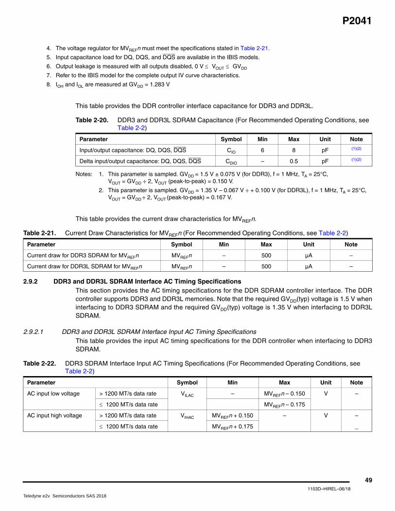
P2041
4. The voltage regulator for MVREFn must meet the specifications stated in Table 2-21.
5. Input capacitance load for DQ, DQS, and DQS are available in the IBIS models.
6. Output leakage is measured with all outputs disabled, 0 V VOUT GVDD
7. Refer to the IBIS model for the complete output IV curve characteristics.
8. IOH and IOL are measured at GVDD = 1.283 V
This table provides the DDR controller interface capacitance for DDR3 and DDR3L.
Notes: 1. This parameter is sampled. GVDD = 1.5 V ± 0.075 V (for DDR3), f = 1 MHz, TA = 25°C,VOUT = GVDD ÷ 2, VOUT (peak-to-peak) = 0.150 V.
2. This parameter is sampled. GVDD = 1.35 V – 0.067 V ÷ + 0.100 V (for DDR3L), f = 1 MHz, TA = 25°C,VOUT = GVDD ÷ 2, VOUT (peak-to-peak) = 0.167 V.
This table provides the current draw characteristics for MVREFn.
2.9.2 DDR3 and DDR3L SDRAM Interface AC Timing Specifications This section provides the AC timing specifications for the DDR SDRAM controller interface. The DDRcontroller supports DDR3 and DDR3L memories. Note that the required GVDD(typ) voltage is 1.5 V wheninterfacing to DDR3 SDRAM and the required GVDD(typ) voltage is 1.35 V when interfacing to DDR3LSDRAM.
2.9.2.1 DDR3 and DDR3L SDRAM Interface Input AC Timing Specifications This table provides the input AC timing specifications for the DDR controller when interfacing to DDR3SDRAM.
Table 2-20. DDR3 and DDR3L SDRAM Capacitance (For Recommended Operating Conditions, see Table 2-2)
Parameter Symbol Min Max Unit Note
Input/output capacitance: DQ, DQS, DQS CIO 6 8 pF (1)(2)
Delta input/output capacitance: DQ, DQS, DQS CDIO – 0.5 pF (1)(2)
Table 2-21. Current Draw Characteristics for MVREFn (For Recommended Operating Conditions, see Table 2-2)
Parameter Symbol Min Max Unit Note
Current draw for DDR3 SDRAM for MVREFn MVREFn – 500 µA –
Current draw for DDR3L SDRAM for MVREFn MVREFn – 500 µA –
Table 2-22. DDR3 SDRAM Interface Input AC Timing Specifications (For Recommended Operating Conditions, see Table 2-2)
Parameter Symbol Min Max Unit Note
AC input low voltage > 1200 MT/s data rate VILAC – MVREFn – 0.150 V –
1200 MT/s data rate MVREFn – 0.175
AC input high voltage > 1200 MT/s data rate VIHAC MVREFn + 0.150 – V –
1200 MT/s data rate MVREFn + 0.175 _
491103D–HIREL–06/18
Teledyne e2v Semiconductors SAS 2018

P2041
This table provides the input AC timing specifications for the DDR controller when interfacing to DDR3LSDRAM.
This table provides the input AC timing specifications for the DDR controller when interfacing to DDR3SDRAM.
Notes: 1. tCISKEW represents the total amount of skew consumed by the controller between MDQS[n] and any corresponding bit that is captured with MDQS[n]. This must be subtracted from the total timing budget.
2. The amount of skew that can be tolerated from MDQS to a corresponding MDQ signal is called tDISKEW.This can be determined by the following equation: tDISKEW = ±(T ÷ 4 – abs(tCISKEW)) where T is the clock period and abs(tCISKEW) is the absolute value of tCISKEW.
Table 2-23. DDR3L SDRAM Interface Input AC Timing Specifications (For Recommended Operating Conditions, see Table 2-2)
Parameter Symbol Min Max Unit Note
AC input low voltage > 1200 MT/s data rate VILAC – MVREFn – 0.135 V –
1200 MT/s data rate – MVREFn – 0.160
AC input high voltage > 1200 MT/s data rate VIHAC MVREFn + 0.135 – V –
1200 MT/s data rate MVREFn + 0.160 –
Table 2-24. DDR3 and DDR3L SDRAM Interface Input AC Timing Specifications (For Recommended Operating Conditions, see Table 2-2)
Parameter Symbol Min Max Unit Note
Controller Skew for MDQS—MDQ/MECC1333 MT/s data rate
1200 MT/s data rate
1066 MT/s data rate800 MT/s data rate
tCISKEW
–125
–142
–170–200
125
142
170200
ps (1)
Tolerated Skew for MDQS—MDQ/MECC1333 MT/s data rate
1200 MT/s data rate
1066 MT/s data rate800 MT/s data rate
tDISKEW
–250
–275
–300–425
250
275
300425
ps (2)
501103D–HIREL–06/18
Teledyne e2v Semiconductors SAS 2018

P2041
Figure 2-3. DDR3 and DDR3L SDRAM Interface Input Timing Diagram
2.9.2.2 DDR3 and DDDR3L SDRAM Interface Output AC Timing Specifications This table provides the DDR3/DDR3L SDRAM output AC timing specifications.
MCK[n]
MCK[n]tMCK
MDQ[x]
MDQS[n]
tDISKEW
D1D0
tDISKEW
tDISKEW
Table 2-25. DDR3 and DDR3L SDRAM Interface Output AC Timing Specifications (For Recommended Operating Conditions, see Table 2-2)
Parameter Symbol(1) Min Max Unit Note
MCK[n] cycle time tMCK 1.5 2.5 ns (2)
ADDR/CMD output setup with respect to MCK tDDKHAS ns (3)
1333 MT/s data rate 0.606 –
1200 MT/s data rate 0.675 –
1066 MT/s data rate 0.744 –
800 MT/s data rate 0.917 –
ADDR/CMD output hold with respect to MCK tDDKHAX ns (3)
1333 MT/s data rate 0.606 –
1200 MT/s data rate 0.675 –
1066 MT/s data rate 0.744 –
800 MT/s data rate 0.917 –
MCS[n] output setup with respect to MCK tDDKHCS ns (3)
1333 MT/s data rate 0.606 –
1200 MT/s data rate 0.675 –
1066 MT/s data rate 0.744 –
800 MT/s data rate 0.917 –
MCS[n] output hold with respect to MCK tDDKHCX ns (3)
1333 MT/s data rate 0.606 –
1200 MT/s data rate 0.675 –
1066 MT/s data rate 0.744 –
800 MT/s data rate 0.917 –
511103D–HIREL–06/18
Teledyne e2v Semiconductors SAS 2018

P2041
Notes: 1. The symbols used for timing specifications follow the pattern of t(first two letters of functional block)(signal)(state) (reference)(state) for inputs
and t(first two letters of functional block)(reference)(state)(signal)(state) for outputs. Output hold time can be read as DDR timing (DD) from the rising or falling edge of the reference clock (KH or KL) until the output went invalid (AX or DX). For example, tDDKHAS
symbolizes DDR timing (DD) for the time tMCK memory clock reference (K) goes from the high (H) state until outputs (A) are setup (S) or output valid time. Also, tDDKLDX symbolizes DDR timing (DD) for the time tMCK memory clock reference (K) goes low (L) until data outputs (D) are invalid (X) or data output hold time.
2. All MCK/MCK and MDQS/MDQS referenced measurements are made from the crossing of the two signals.
3. ADDR/CMD includes all DDR SDRAM output signals except MCK/MCK, MCS, and MDQ/MECC/MDM/MDQS.
4. Note that tDDKHMH follows the symbol conventions described in note 1. For example, tDDKHMH describes the DDR timing (DD) from the rising edge of the MCK[n] clock (KH) until the MDQS signal is valid (MH). tDDKHMH can be modified through control of the MDQS override bits (called WR_DATA_DELAY) in the TIMING_CFG_2 register. This is typically set to the same delay as in DDR_SDRAM_CLK_CNTL[CLK_ADJUST]. The timing parameters listed in the table assume that these two parameters have been set to the same adjustment value. See the chip reference manual for a description and explanation of the timing modifications enabled by use of these bits.
5. Determined by maximum possible skew between a data strobe (MDQS) and any corresponding bit of data (MDQ), ECC (MECC), or data mask (MDM). The data strobe must be centered inside of the data eye at the pins of the microprocessor.
6. Note that for 1200/1333 frequencies it is required to program the start value of the DQS adjust for write leveling.
NOTE
For the ADDR/CMD setup and hold specifications in Table 2-25 on page 51, it is assumed that the clockcontrol register is set to adjust the memory clocks by ½ applied cycle.
This figure shows the DDR3 and DDR3L SDRAM interface output timing for the MCK to MDQS skewmeasurement (tDDKHMH)
.
MCK to MDQS Skew tDDKHMH ns (4)
> 1066 MT/s data rate –0.245 0.245 (4)(6)
800 MT/s data rate –0.375 0.375 (4)
MDQ/MECC/MDM output setup with respect to MDQS tDDKHDS, tDDKLDS ps (5)
1333 MT/s data rate 250 –
1200 MT/s data rate 275 –
1066 MT/s data rate 300 –
800 MT/s data rate 375 –
MDQ/MECC/MDM output hold with respect to MDQS tDDKHDX, tDDKLDX ps (5)
1333 MT/s data rate 250 –
1200 MT/s data rate 275 –
1066 MT/s data rate 300 –
800 MT/s data rate 375 –
MDQS preamble tDDKHMP 0.9 × tMCK – ns –
MDQS postamble tDDKHME 0.4 × tMCK 0.6 × tMCK ns –
Table 2-25. DDR3 and DDR3L SDRAM Interface Output AC Timing Specifications (For Recommended Operating Conditions, see Table 2-2) (Continued)
Parameter Symbol(1) Min Max Unit Note
521103D–HIREL–06/18
Teledyne e2v Semiconductors SAS 2018

P2041
Figure 2-4. tDDKHMH Timing Diagram
This figure shows the DDR3 and DDR3L SDRAM output timing diagram.
Figure 2-5. DDR3 and DDR3L Output Timing Diagram
This figure provides the AC test load for the DDR3 and DDR3L controller bus.
Figure 2-6. DDR3 and DDR3L Controller Bus AC Test Load
MDQS
MCK[n]
MCK[n]tMCK
tDDKHMHmax)
tDDKHMH(min)
MDQS
ADDR/CMD
tDDKHAS, tDDKHCS
tDDKLDS
tDDKHDS
MDQ[x]
MDQS[n]
MCK
MCKtMCK
tDDKLDX
tDDKHDX
D1D0
tDDKHAX, tDDKHCX
Write A0 NOOP
tDDKHME
tDDKHMH
tDDKHMP
Output Z0 = 50Ω GVDD/2RL = 50Ω
531103D–HIREL–06/18
Teledyne e2v Semiconductors SAS 2018

P2041
2.9.2.3 DDR3 and DDR3L SDRAM Differential Timing Specifications This section describes the DC and AC differential timing specifications for the DDR3 and DDR3LSDRAM controller interface. This figure shows the differential timing specification.
Figure 2-7. DDR3 and DDR3L SDRAM Differential Timing Specifications
NOTEVTR specifies the true input signal (such as MCK or MDQS) and VCP is the complementary input signal(such as MCK or MDQS).
This table provides the DDR3 differential specifications for the differential signals MDQS/MDQS andMCK/MCK.
Note: 1. I/O drivers are calibrated before making measurements.
This table provides the DDR3L differential specifications for the differential signals MDQS/MDQS andMCK/MCK.
Note: 1. I/O drivers are calibrated before making measurements.
VTR
VCP
GND
GVDD
VOX or VIX
GVDD/2
Table 2-26. DDR3 SDRAM Differential Electrical Characteristics(1)
Parameter Symbol Min Max Unit Note
Input AC Differential Cross-Point Voltage VIXAC 0.5 × GVDD – 0.150 0.5 × GVDD + 0.150 V –
Output AC Differential Cross-Point Voltage VOXAC 0.5 × GVDD – 0.115 0.5 × GVDD + 0.115 V –
Table 2-27. DDR3L SDRAM Differential Electrical Characteristics(1)
Parameter Symbol Min Max Unit Note
Input AC differential cross-point voltage VIXAC 0.5 × GVDD – 0.135 0.5 × GVDD + 0.135 V –
Output AC differential cross-point voltage VOXAC 0.5 × GVDD – 0.105 0.5 × GVDD + 0.105 V –
541103D–HIREL–06/18
Teledyne e2v Semiconductors SAS 2018

P2041
2.10 eSPI This section describes the DC and AC electrical specifications for the eSPI interface.
2.10.1 eSPI DC Electrical Characteristics This table provides the DC electrical characteristics for the eSPI interface operating at CVDD = 3.3 V.
Notes: 1. The min VIL and max VIH values are based on the respective min and max CVIN values found in Table 2-2.
2. The symbol VIN, in this case, represents the CVIN symbol referenced in Section 2.1.2 ”Recommended Operating Conditions” on page 35.
This table provides the DC electrical characteristics for the eSPI interface operating at CVDD = 2.5 V.
Notes: 1. The min VIL and max VIH values are based on the respective min and max CVIN values found in Table 2-2.
2. The symbol VIN, in this case, represents the CVIN symbol referenced in Section 2.1.2 ”Recommended Operating Conditions” on page 35.
Table 2-28. eSPI DC Electrical Characteristics (CVDD = 3.3 V) (For Recommended Operating Conditions, see Table 2-2)
Parameter Symbol Min Max Unit Note
Input high voltage VIH 2.0 – V (1)
Input low voltage VIL – 0.8 V (1)
Input current (VIN = 0 V or VIN = CVDD) IIN – ±40 µA (2)
Output high voltage (CVDD = min, IOH = –2 mA) VOH 2.4 – V –
Output low voltage (CVDD = min, IOL = 2 mA) VOL – 0.4 V –
Table 2-29. eSPI DC Electrical Characteristics (CVDD = 2.5 V) (For Recommended Operating Conditions, see Table 2-2)
Parameter Symbol Min Max Unit Note
Input high voltage VIH 1.7 – V (1)
Input low voltage VIL – 0.7 V (1)
Input current (VIN = 0 V or VIN = CVDD) IIN – ±40 µA (2)
Output high voltage (CVDD = min, IOH = –1 mA) VOH 2.0 – V –
Output low voltage (CVDD = min, IOL = 1 mA) VOL – 0.4 V –
551103D–HIREL–06/18
Teledyne e2v Semiconductors SAS 2018

P2041
This table provides the DC electrical characteristics for the eSPI interface operating at CVDD = 1.8 V.
Notes: 1. The min VIL and max VIH values are based on the respective min and max CVIN values found in Table 2-2.
2. The symbol VIN, in this case, represents the CVIN symbol referenced in Section 2.1.2 ”Recommended Operating Conditions” on page 35.
2.10.2 eSPI AC Timing Specifications This table provides the eSPI input and output AC timing specifications.
Notes: 1. The symbols used for timing specifications follow the pattern of t(first two letters of functional block)(signal)(state) (reference)(state) for inputs
and t(first two letters of functional block)(reference)(state)(signal)(state) for outputs. For example, tNIKHOV symbolizes the NMSI outputs internal timing (NI) for the time tSPI memory clock reference (K) goes from the high state (H) until outputs (O) are valid (V).
2. Output specifications are measured from the 50% level of the rising edge of CLKIN to the 50% level of the signal. Timings are measured at the pin.
3. The greater of the two output timings for tNIKHOX and tNIKHOV are used when SPCOM[RxDelay] of the eSPI command register is set. For example, the tNIKHOX is 4.0 and tNIKHOV is 7.0 if SPCOM[RxDelay] is set to be 1.
This figure provides the AC test load for the eSPI.
Figure 2-8. eSPI AC Test Load
Table 2-30. eSPI DC Electrical Characteristics (CVDD = 1.8 V) (For Recommended Operating Conditions, see Table 2-2)
Parameter Symbol Min Max Unit Note
Input high voltage VIH 1.25 – V (1)
Input low voltage VIL – 0.6 V (1)
Input current (VIN = 0 V or VIN = CVDD) IIN – ±40 µA (2)
Output high voltage (CVDD = min, IOH = –0.5 mA) VOH 1.35 – V –
Output low voltage (CVDD = min, IOL = 0.5 mA) VOL – 0.4 V –
Table 2-31. eSPI AC Timing Specifications (For Recommended Operating Conditions, see Table 2-2)
Parameter Symbol(1) Min Max Unit Note
SPI_MOSI output—Master data (internal clock) hold time tNIKHOX 2+(tPLATFORM_CLK*
SPMODE[HO_ADJ]) –
ns (2)(3)
SPI_MOSI output—Master data (internal clock) delay tNIKHOV
tNIKHOV –
5.68+(tPLATFORM_CLK*SPMODE[HO_ADJ])
ns (2)(3)
SPI_CS outputs—Master data (internal clock) hold time tNIKHOX2 0 – ns (2)
SPI_CS outputs—Master data (internal clock) delay tNIKHOV2 – 6.0 ns (2)
eSPI inputs—Master data (internal clock) input setup time tNIIVKH 7 – ns –
eSPI inputs—Master data (internal clock) input hold time tNIIXKH 0 – ns –
Output Z0 = 50Ω CVDD/2RL = 50Ω
561103D–HIREL–06/18
Teledyne e2v Semiconductors SAS 2018

P2041
This figure represents the AC timing from Table 2-31 in master mode (internal clock). Note that althoughtiming specifications generally refer to the rising edge of the clock, this figure also applies when thefalling edge is the active edge. Also, note that the clock edge is selectable on eSPI.
Figure 2-9. eSPI AC Timing in Master Mode (Internal Clock) Diagram
2.11 DUART This section describes the DC and AC electrical specifications for the DUART interface.
2.11.1 DUART DC Electrical Characteristics This table provides the DC electrical characteristics for the DUART interface.
Notes: 1. The symbol OVIN, in this case, represents the OVIN symbol referenced in Table 2-2.
2. The symbol OVIN, in this case, represents the OVIN symbol referenced in Section 2.1.2 ”Recommended Operating Conditions” on page 35.
SPICLK (output)
tNIIXKH
tNIKHOV
Input signals:SPIMISO1
Output signals:SPIMOSI1
tNIIVKH
tNIKHOX
Output signals:SPI_CS[0:3]1
tNIKHOV2 tNIKHOX2
Table 2-32. DUART DC Electrical Characteristics (OVDD = 3.3 V) (For Recommended Operating Conditions, see Table 2-2)
Parameter Symbol Min Max Unit Note
Input high voltage VIH 2 – V (1)
Input low voltage VIL – 0.8 V (1)
Input current (OVIN = 0 V or OVIN = OVDD) IIN – ±40 µA (2)
Output high voltage (OVDD = min, IOH = –2 mA) VOH 2.4 – V –
Output low voltage (OVDD = min, IOL = 2 mA) VOL – 0.4 V –
571103D–HIREL–06/18
Teledyne e2v Semiconductors SAS 2018

P2041
2.11.2 DUART AC Electrical Specifications This table provides the AC timing parameters for the DUART interface.
Notes: 1. fPLAT refers to the internal platform clock.
2. The actual attainable baud rate is limited by the latency of interrupt processing.
3. The middle of a start bit is detected as the eighth sampled 0 after the 1-to-0 transition of the start bit. Subsequent bit values are sampled every 16th sample.
2.12 Ethernet: Data path Three-Speed Ethernet (dTSEC), Management Interface, IEEE Std 1588
This section provides the AC and DC electrical characteristics for the data path three-speed Ethernetcontroller, the Ethernet Management Interface, and the IEEE Std 1588 interface.
2.12.1 SGMII Timing Specifications See Section 2.20.9 ”SGMII Interface” on page 105.
2.12.2 RGMII Timing Specifications This section discusses the electrical characteristics for the MII and RGMII interfaces.
2.12.2.1 RGMII DC Electrical Characteristics This table shows the RGMII DC electrical characteristics when operating at LVDD = 2.5 V supply.
Notes: 1. The min VIL and max VIH values are based on the respective min and max LVIN values found in Table 2-2.
2. The symbol VIN, in this case, represents the LVIN symbols referenced in Table 2-1 and Table 2-2.
Table 2-33. DUART AC Timing Specifications (For Recommended Operating Conditions, see Table 2-2)
Parameter Value Unit Note
Minimum baud rate fPLAT/(2 × 1,048,576) baud (1)
Maximum baud rate fPLAT/(2 × 16) baud (1)(2)
Oversample rate 16 – (3)
Table 2-34. RGMII DC Electrical Characteristics (LVDD = 2.5 V) (For Recommended Operating Conditions, see Table 2-2)
Parameter Symbol Min Max Unit Note
Input high voltage VIH 1.70 – V (1)
Input low voltage VIL – 0.70 V (1)
Input current (LVIN = 0 V or LVIN = LVDD) IIH – ±40 µA (2)
Output high voltage (LVDD = min, IOH = –1.0 mA) VOH 2.00 – V –
Output low voltage (LVDD = min, IOL = 1.0 mA) VOL – 0.40 V –
581103D–HIREL–06/18
Teledyne e2v Semiconductors SAS 2018

P2041
2.12.2.2 RGMII AC Timing Specifications This table shows the RGMII AC timing specifications.
Notes: 1. In general, the clock reference symbol representation for this section is based on the symbols RGT to represent RGMII timing. Note that the notation for rise (R) and fall (F) times follows the clock symbol that is being represented. For symbols representing skews, the subscript is skew (SK) followed by the clock that is being skewed (RGT).
2. This implies that PC board design requires clocks to be routed such that an additional trace delay of greater than 1.5 ns is added to the associated clock signal. Many PHY vendors already incorporate the necessary delay inside their chip. If so, additional PCB delay is probably not needed.
3. For 10 and 100 Mbps, tRGT scales to 400 ns ± 40 ns and 40 ns ± 4 ns, respectively.
4. Duty cycle may be stretched/shrunk during speed changes or while transitioning to a received packet's clock domains as long as the minimum duty cycle is not violated and stretching occurs for no more than three tRGT of the lowest speed transitioned between.
5. The frequency of RX_CLK should not exceed the frequency of GTX_CLK125 by more than 300 ppm.
Table 2-35. RGMII AC Timing Specifications (For Recommended Operating Conditions, see Table 2-2)
Parameter/Condition Symbol(1) Min Typ Max Unit Note
Data to clock output skew (at transmitter) tSKRGT_TX –500 0 500 ps (5)
Data to clock input skew (at receiver) tSKRGT_RX 1.0 – 2.8 ns (2)
Clock period duration tRGT 7.2 8.0 8.8 ns (3)
Duty cycle for 10BASE-T and 100BASE-TX tRGTH/tRGT 40 50 60 % (3)(4)
Duty cycle for Gigabit tRGTH/tRGT 45 50 55 % –
Rise time (20%–80%) tRGTR – – 0.75 ns –
Fall time (20%–80%) tRGTF – – 0.75 ns –
591103D–HIREL–06/18
Teledyne e2v Semiconductors SAS 2018

P2041
Figure 2-10. RGMII AC Timing and Multiplexing Diagrams
GTX_CLK
tRGTtRGTH
tSKRGT_TX
TX_CTL
TXD[8:5]TXD[7:4]
TXD[9]TXERR
TXD[4]TXEN
TXD[3:0]
(At MAC, output)
TXD[8:5][3:0]TXD[7:4][3:0]
TX_CLK(At PHY, input)
RX_CTL
RXD[8:5]RXD[7:4]
RXD[9]RXERR
RXD[4]RXDV
RXD[3:0]
RX_CLK(At MAC, input)
tSKRGT_RX
tRGTHtRGT
RX_CLK(At PHY, output)
RXD[8:5][3:0]RXD[7:4][3:0]
tSKRGT_RX
PHY equivalent to tSKRGT_TX
tSKRGT_TX
PHY equivalent to tSKRGT_RXPHY equivalent to tSKRGT_RX
(At MAC, output)
(At MAC, output)
(At PHY, output)
(At PHY, output)
PHY equivalent to tSKRGT_TX
601103D–HIREL–06/18
Teledyne e2v Semiconductors SAS 2018

P2041
2.12.3 Ethernet Management Interface This section discusses the electrical characteristics for the EMI1 and EMI2 interfaces. EMI1 is the PHYmanagement interface controlled by the MDIO controller associated with Frame Manager 1 1GMAC–1.EMI2 is the XAUI PHY management interface controlled by the MDIO controller associated with FrameManager 1 10GMAC–0.
2.12.3.1 Ethernet Management Interface DC Electrical Characteristics The Ethernet management interface is defined to operate at a supply voltage of 3.3 V. The DC electricalcharacteristics for the Ethernet management interface is provided in this table.
Notes: 1. The symbol VIN, in this case, represents the LVIN symbol referenced in Table 2-1 and Table 2-2.
2. The min VIL and max VIH values are based on the respective LVIN values found in Table 2-2.
The Ethernet management interface is defined to operate at a supply voltage of 2.5 V. The DC electricalcharacteristics for the Ethernet management interface is provided in this table.
Notes: 1. The min VIL and max VIH values are based on the respective min and max LVIN values found in Table 2-2.
2. The symbol LVIN, in this case, represents the LVIN symbol referenced in Section 2.1.2 ”Recommended Operating Conditions” on page 35.
Table 2-36. Ethernet Management Interface 1 DC Electrical Characteristics (LVDD = 3.3 V) (For Recommended Operating Conditions, see Table 2-2)
Parameter Symbol Min Max Unit Note
Input high voltage VIH 2.0 – V (2)
Input low voltage VIL – 0.9 V (2)
Input high current (LVDD = Max, VIN = 2.1 V) IIH – 40 µA (1)
Input low current (LVDD = Max, VIN = 0.5 V) IIL –600 – µA (1)
Output high voltage (LVDD = Min, IOH = –1.0 mA) VOH 2.4 – V –
Output low voltage (LVDD = Min, IOL = 1.0 mA) VOL – 0.4 V –
Table 2-37. Ethernet Management Interface 1 DC Electrical Characteristics (LVDD = 2.5 V) (For Recommended Operating Conditions, see Table 2-2)
Parameter Symbol Min Max Unit Note
Input high voltage VIH 1.7 – V (1)
Input low voltage VIL – 0.7 V (1)
Input current (LVIN = 0 V or LVIN = LVDD) IIH – ±40 µA (2)
Output high voltage (LVDD = Min, IOH = –1.0 mA) VOH 2.0 – V –
Output low voltage (LVDD = Min, IOL = 1.0 mA) VOL – 0.4 V –
611103D–HIREL–06/18
Teledyne e2v Semiconductors SAS 2018

P2041
2.12.3.2 Ethernet Management Interface 2 DC Electrical Characteristics Ethernet Management Interface 2 pins function as open drain I/Os. The interface shall conform to 1.2 Vnominal voltage levels. LVDD must be powered to use this interface. The DC electrical characteristics forEMI2_MDIO and EMI2_MDC are provided in this table.
2.12.3.3 Ethernet Management Interface 1 AC Timing Specifications This table provides the Ethernet management interface 1 AC timing specifications.
Notes: 1. The symbols used for timing specifications follow the pattern of t(first two letters of functional block)(signal)(state)(reference)(state) for inputs and
t(first two letters of functional block)(reference)(state)(signal)(state) for outputs. For example, tMDKHDX symbolizes management data timing (MD) for the time tMDC from clock reference (K) high (H) until data outputs (D) are invalid (X) or data hold time. Also, tMDDVKH symbolizes management data timing (MD) with respect to the time data input signals (D) reaching the valid state (V) relative to the tMDC clock reference (K) going to the high (H) state or setup time. For rise and fall times, the latter convention is used with the appropriate letter: R (rise) or F (fall).
2. This parameter is dependent on the platform clock frequency (MIIMCFG [MgmtClk] field determines the clock frequency of the MgmtClk Clock EC_MDC).
3. This parameter is dependent on the platform clock frequency. The delay is equal to 16 platform clock periods ±3 ns. For example, with a platform clock of 333 MHz, the min/max delay is 48 ns ± 3 ns. Similarly, if the platform clock is 400 MHz, the min/max delay is 40 ns ± 3 ns.
4. tplb_clk is the frame manager clock period.
Table 2-38. Ethernet Management Interface 2 DC Electrical Characteristics (1.2 V) (For Recommended Operating Conditions, see Table 2-2)
Parameter Symbol Min Max Unit Note
Input high voltage VIH 0.84 – V –
Input low voltage VIL – 0.36 V –
Output high voltage (IOH = –100 µA) VOH 1.0 – V –
Output low voltage (IOL = 100 µA) VOL – 0.2 V –
Output low current (VOL = 0.2 V) IOL 4 – mA –
Input capacitance CIN – 10 pF –
Table 2-39. Ethernet Management Interface 1 AC Timing Specifications (For Recommended Operating Conditions, see Table 2-2)
Parameter Symbol(1) Min Typ Max Unit Note
MDC frequency fMDC – – 2.5 MHz (2)
MDC clock pulse width high tMDCH 160 – – ns –
MDC to MDIO delay tMDKHDX (16 × tplb_clk) – 6 – (16 × tplb_clk) + 6 ns (3)(4)
MDIO to MDC setup time tMDDVKH 10 – – ns –
MDIO to MDC hold time tMDDXKH 0 – – ns –
621103D–HIREL–06/18
Teledyne e2v Semiconductors SAS 2018

P2041
2.12.3.4 Ethernet Management Interface 2 AC Electrical Characteristics This table provides the Ethernet management interface 2 AC timing specifications.
Notes: 1. The symbols used for timing specifications follow the pattern of t(first two letters of functional block)(signal)(state)(reference)(state) for inputs and
t(first two letters of functional block)(reference)(state)(signal)(state) for outputs. For example, tMDKHDX symbolizes management data timing (MD) for the time tMDC from clock reference (K) high (H) until data outputs (D) are invalid (X) or data hold time. Also, tMDDVKH symbolizes management data timing (MD) with respect to the time data input signals (D) reach the valid state (V) relative to the tMDC clock reference (K) going to the high (H) state or setup time.
2. This parameter is dependent on the frame manager clock frequency (MIIMCFG [MgmtClk] field determines the clock frequency of the MgmtClk Clock EC_MDC).
3. This parameter is dependent on the management data clock frequency, fMDC. The delay is equal to 0.5 management data clock period ±6 ns. For example, with a management data clock of 2.5 MHz, the min/max delay is 200 ns ± 6 ns.
This figure shows the Ethernet management interface timing diagram.
Figure 2-11. Ethernet Management Interface Timing Diagram
Table 2-40. Ethernet Management Interface 2 AC Timing Specifications (For Recommended Operating Conditions, see Table 2-2)
Parameter/Condition Symbol(1) Min Typ Max Unit Note
MDC frequency fMDC – – 2.5 MHz (2)
MDC clock pulse width high tMDCH 160 – – ns –
MDC to MDIO delay tMDKHDX (0.5 ×(1/fMDC)) – 6 – (0.5 ×(1/fMDC)) + 6 ns (3)
MDIO to MDC setup time tMDDVKH 10 – – ns –
MDIO to MDC hold time tMDDXKH 0 – – ns –
MDC
tMDDXKH
tMDC
tMDCH
tMDDVKH
tMDKHDX
MDIO
MDIO
(Input)
(Output)
631103D–HIREL–06/18
Teledyne e2v Semiconductors SAS 2018
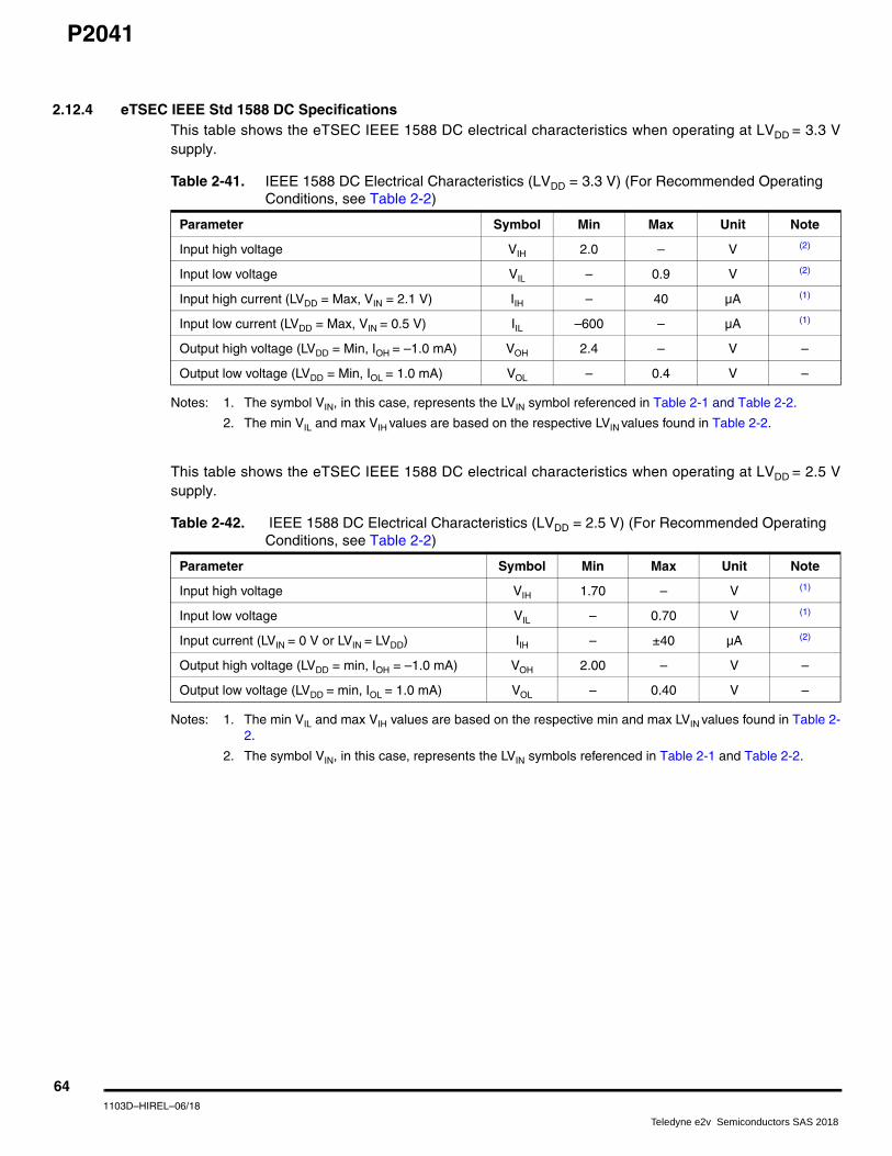
P2041
2.12.4 eTSEC IEEE Std 1588 DC Specifications This table shows the eTSEC IEEE 1588 DC electrical characteristics when operating at LVDD = 3.3 Vsupply.
Notes: 1. The symbol VIN, in this case, represents the LVIN symbol referenced in Table 2-1 and Table 2-2.
2. The min VIL and max VIH values are based on the respective LVIN values found in Table 2-2.
This table shows the eTSEC IEEE 1588 DC electrical characteristics when operating at LVDD = 2.5 Vsupply.
Notes: 1. The min VIL and max VIH values are based on the respective min and max LVIN values found in Table 2-2.
2. The symbol VIN, in this case, represents the LVIN symbols referenced in Table 2-1 and Table 2-2.
Table 2-41. IEEE 1588 DC Electrical Characteristics (LVDD = 3.3 V) (For Recommended Operating Conditions, see Table 2-2)
Parameter Symbol Min Max Unit Note
Input high voltage VIH 2.0 – V (2)
Input low voltage VIL – 0.9 V (2)
Input high current (LVDD = Max, VIN = 2.1 V) IIH – 40 µA (1)
Input low current (LVDD = Max, VIN = 0.5 V) IIL –600 – µA (1)
Output high voltage (LVDD = Min, IOH = –1.0 mA) VOH 2.4 – V –
Output low voltage (LVDD = Min, IOL = 1.0 mA) VOL – 0.4 V –
Table 2-42. IEEE 1588 DC Electrical Characteristics (LVDD = 2.5 V) (For Recommended Operating Conditions, see Table 2-2)
Parameter Symbol Min Max Unit Note
Input high voltage VIH 1.70 – V (1)
Input low voltage VIL – 0.70 V (1)
Input current (LVIN = 0 V or LVIN = LVDD) IIH – ±40 µA (2)
Output high voltage (LVDD = min, IOH = –1.0 mA) VOH 2.00 – V –
Output low voltage (LVDD = min, IOL = 1.0 mA) VOL – 0.40 V –
641103D–HIREL–06/18
Teledyne e2v Semiconductors SAS 2018

P2041
2.12.5 eTSEC IEEE Std 1588 AC Specifications This table provides the eTSEC IEEE 1588 AC timing specifications.
Notes: 1. TRX_CLK is the maximum clock period of eTSEC receiving clock selected by TMR_CTRL[CKSEL]. See the chip reference manual for a description of TMR_CTRL registers.
2. The maximum value of tT1588CLK is not only defined by the value of TRX_CLK, but also defined by the recovered clock. For example, for 10/100/1000 Mbps modes, the maximum value of tT1588CLK is 2800, 280, and 56 ns, respectively.
3. It needs to be at least two times the clock period of the clock selected by TMR_CTRL[CKSEL]. See the chip reference manual for a description of TMR_CTRL registers.
This figure shows the data and command output AC timing diagram.
Figure 2-12. eTSEC IEEE 1588 Output AC Timing
Note: The output delay is counted starting at the rising edge if tT1588CLKOUT is non inverting. Otherwise, it is counted starting at the falling edge.
Table 2-43. eTSEC IEEE 1588 AC Timing Specifications (For Recommended Operating Conditions, see Table 2-2)
Parameter Symbol Min Typ Max Unit Note
TSEC_1588_CLK clock period tT1588CLK 6.4 – TRX_CLK × 7 ns (1)(2)
TSEC_1588_CLK duty cycle tT1588CLKH/ tT1588CLK
40 50 60 % (3)
TSEC_1588_CLK peak-to-peak jitter tT1588CLKINJ – – 250 ps –
Rise time eTSEC_1588_CLK (20%–80%) tT1588CLKINR 1.0 – 2.0 ns –
Fall time eTSEC_1588_CLK (80%–20%) tT1588CLKINF 1.0 – 2.0 ns –
TSEC_1588_CLK_OUT clock period tT1588CLKOUT 2 × tT1588CLK – – ns –
TSEC_1588_CLK_OUT duty cycle tT1588CLKOTH/ tT1588CLKOUT
30 50 70 % –
TSEC_1588_PULSE_OUT tT1588OV 0.5 – 3.5 ns –
TSEC_1588_TRIG_IN pulse width tT1588TRIGH 2 × tT1588CLK_MAX – – ns (2)
TSEC_1588_CLK_OUT
TSEC_1588_PULSE_OUTTSEC_1588_TRIG_OUT
tT1588OV
tT1588CLKOUT
tT1588CLKOUTH
651103D–HIREL–06/18
Teledyne e2v Semiconductors SAS 2018

P2041
This figure shows the data and command input AC timing diagram.
Figure 2-13. eTSEC IEEE 1588 Input AC Timing
2.13 USB This section provides the AC and DC electrical specifications for the USB interface.
2.13.1 USB DC Electrical Characteristics This table provides the DC electrical characteristics for the USB interface at USB_VDD_3P3 = 3.3 V.
Notes: 1. The min VIL and max VIH values are based on the respective min and max USB_VIN_3P3 values found in Table 2-2.
2. The symbol USB_VIN_3P3, in this case, represents the USB_VIN_3P3 symbol referenced in Section 2.1.2 ”Recommended Operating Conditions” on page 35.
2.13.2 USB AC Electrical Specifications This table provides the USB clock input (USBn_CLKIN) AC timing specifications.
Note: 1. System/board must be designed to ensure the input requirement to the device is achieved. Proper device operation is guaranteed for inputs meeting this requirement by design, simulation, characterization, or functional testing.
TSEC_1588_TRIG_INtT1588TRIGH
tT1588CLK
tT1588CLKH
TSEC_1588_CLK
Table 2-44. USB DC Electrical Characteristics (USB_VDD_3P3 = 3.3 V) (For Recommended Operating Conditions, see Table 2-2)
Parameter Symbol Min Max Unit Note
Input high voltage(1) VIH 2.0 – V (1)
Input low voltage VIL – 0.8 V (1)
Input current (USB_VIN_3P3 = 0 V or USB_VIN_3P3 = USB_VDD_3P3) IIN – ±40 µA (2)
Output high voltage (USB_VDD_3P3 = min, IOH = –2 mA) VOH 2.8 – V
Output low voltage (USB_VDD_3P3 = min, IOL = 2 mA) VOL – 0.3 V –
Table 2-45. USB_CLK_IN AC Timing Specifications (For Recommended Operating Conditions, see Table 2-2)
Parameter Condition Symbol Min Typical Max Unit Note
Frequency range – fUSB_CLK_IN – 24 – MHz –
Rise/Fall time Measured between 10% and 90% tUSRF – – 6 ns (1)
Clock frequency tolerance – tCLK_TOL –0.005 0 0.005 % –
Reference clock duty cycle Measured at 1.6 V tCLK_DUTY 40 50 60 % –
Total input jitter/time interval error
RMS value measured with a second-order, high-pass filter of 500-kHz bandwidth
tCLK_PJ – – 5 ps –
661103D–HIREL–06/18
Teledyne e2v Semiconductors SAS 2018

P2041
2.14 Enhanced Local Bus Interface This section describes the DC and AC electrical specifications for the enhanced local bus interface.
2.14.1 Enhanced Local Bus DC Electrical Characteristics This table provides the DC electrical characteristics for the enhanced local bus interface operating atBVDD = 3.3 V.
Notes: 1. The min VIL and max VIH values are based on the respective min and max BVIN values found in Table 2-2.
2. The symbol VIN, in this case, represents the BVIN symbol referenced in Section 2.1.2 ”Recommended Operating Conditions” on page 35.
This table provides the DC electrical characteristics for the enhanced local bus interface operating atBVDD = 2.5 V.
Notes: 1. The min VIL and max VIH values are based on the respective min and max BVIN values found in Table 2-2
2. The symbol VIN, in this case, represents the BVIN symbol referenced in Section 2.1.2 ”Recommended Operating Conditions” on page 35.
Table 2-46. Enhanced Local Bus DC Electrical Characteristics (BVDD = 3.3 V) (For Recommended Operating Conditions, see Table 2-2)
Parameter Symbol Min Max Unit Note
Input high voltage VIH 2 – V (1)
Input low voltage VIL – 0.8 V (1)
Input current (VIN = 0 V or VIN = BVDD) IIN – ±40 µA (2)
Output high voltage (BVDD = min, IOH = –2 mA) VOH 2.4 – V –
Output low voltage (BVDD = min, IOL = 2 mA) VOL – 0.4 V –
Table 2-47. Enhanced Local Bus DC Electrical Characteristics (BVDD = 2.5 V) (For Recommended Operating Conditions, see Table 2-2)
Parameter Symbol Min Max Unit Note
Input high voltage VIH 1.7 – V (1)
Input low voltage VIL – 0.7 V (1)
Input current (VIN = 0 V or VIN = BVDD) IIN – ±40 µA (2)
Output high voltage (BVDD = min, IOH = –1 mA) VOH 2.0 – V –
Output low voltage (BVDD = min, IOL = 1 mA) VOL – 0.4 V –
671103D–HIREL–06/18
Teledyne e2v Semiconductors SAS 2018

P2041
This table provides the DC electrical characteristics for the enhanced local bus interface operating atBVDD = 1.8 V.
Notes: 1. The min VIL and max VIH values are based on the respective min and max BVIN values found in Table 2-2.
2. The symbol VIN, in this case, represents the BVIN symbol referenced in Section 2.1.2 ”Recommended Operating Conditions” on page 35.
2.14.2 Enhanced Local Bus AC Timing Specifications This section describes the AC timing specifications for the enhanced local bus interface.This figure shows the eLBC AC test load.
Figure 2-14. Enhanced Local Bus AC Test Load
Table 2-48. Enhanced Local Bus DC Electrical Characteristics (BVDD = 1.8 V) (For Recommended Operating Conditions, see Table 2-2)
Parameter Symbol Min Max Unit Note
Input high voltage VIH 1.25 – V (1)
Input low voltage VIL – 0.6 V (1)
Input current (VIN = 0 V or VIN = BVDD) IIN – ±40 µA (2)
Output high voltage (BVDD = min, IOH = –0.5 mA) VOH 1.35 – V –
Output low voltage (BVDD = min, IOL = 0.5 mA) VOL – 0.4 V –
Output Z0 = 50Ω BVDD/2RL = 50Ω
681103D–HIREL–06/18
Teledyne e2v Semiconductors SAS 2018

P2041
2.14.2.1 Local Bus AC Timing Specification All output signal timings are relative to the falling edge of any LCLKs. The external circuit must use therising edge of the LCLKs to latch the data.
All input t imings except LGTA/LUPWAIT/LFRB are relative to the rising edge of LCLKs.LGTA/LUPWAIT/LFRB are relative to the falling edge of LCLKs.
This table provides the eLBC timing specifications.
Notes: 1. All signals are measured from BVDD/2 of rising/falling edge of LCLK to BVDD/2 of the signal in question.
2. Skew is measured between different LCLKs at BVDD/2.
3. For purposes of active/float timing measurements, the high impedance or off state is defined to be when the total current delivered through the component pin is less than or equal to the leakage current specification.
4. tLBONOT is a measurement of the minimum time between the negation of LALE and any change in LAD. tLBONOT is determined by LBCR[AHD]. The unit is the eLBC controller clock cycle, which is the internal clock that runs the local bus controller, not the external LCLK. After power on reset, LBCR[AHD] defaults to 0.
5. Output hold is negative, meaning that the output transition happens earlier than the falling edge of LCLK.
Table 2-49. Enhanced Local Bus Timing Specifications (For Recommended Operating Conditions, see Table 2-2)
Parameter Symbol(1) Min Max Unit Note
Local bus cycle time tLBK 12 – ns –
Local bus duty cycle tLBKH/tLBK 45 55 % –
LCLK[n] skew to LCLK[m] tLBKSKEW – 150 ps (2)
Input setup (except LGTA/LUPWAIT/LFRB) tLBIVKH 6 – ns –
Input hold (except LGTA/LUPWAIT/LFRB) tLBIXKH 1 – ns –
Input setup (for LGTA/LUPWAIT/LFRB) tLBIVKL 6 – ns –
Input hold (for LGTA/LUPWAIT/LFRB) tLBIXKL 1 – ns –
Output delay (Except LALE) tLBKLOV – 2.0 ns –
Output hold (Except LALE) tLBKLOX –3.5 – ns (5)
Local bus clock to output high impedance for LAD/LDP tLBKLOZ – 2 ns (3)
LALE output negation to LAD/LDP output transition(LATCH hold time)
tLBONOT2 platform clock cycles -1 ns (LBCR[AHD] = 1)
– ns (4)
4 platform clock cycles -2 ns (LBCR[AHD] = 0
–
691103D–HIREL–06/18
Teledyne e2v Semiconductors SAS 2018

P2041
This figure shows the AC timing diagram of the local bus interface.
Figure 2-15. Enhanced Local Bus Signals
Figure 2-16 applies to all three controllers that eLBC supports: GPCM, UPM, and FCM.
For input signals, the AC timing data is used directly for all three controllers.
For output signals, each type of controller provides its own unique method to control the signal timing.The final signal delay value for output signals is the programmed delay plus the AC timing delay. Forexample, for GPCM, LCS can be programmed to delay by tacs (0, ¼, ½, 1, 1 + ¼, 1 + ½, 2, 3 cycles), sothe final delay is tacs + tLBKLOV.
Output Signals
tLBKLOX
LCLK[m]
Input Signals
LALE
tLBIXKHtLBIVKH
tLBIVKL
tLBIXKL
Input Signal
tLBONOT
(LGTA/LUPWAIT/LFRB)
(except LGTA/LUPWAIT/LFRB)
(except LALE)
LAD(address phase)
LAD/LDP(data phase)
tLBKLOZ
tLBKLOV
701103D–HIREL–06/18
Teledyne e2v Semiconductors SAS 2018

P2041
This figure shows how the AC timing diagram applies to GPCM. The same principle applies to UPM andFCM.
Figure 2-16. GPCM Output Timing Diagram
1. taddr is programmable and determined by LCRR[EADC] and ORx[EAD].
2. tarcs, tawcs, taoe, trc, toen, tawe, twc, twen are determined by ORx. See the chip reference manual.
2.15 Enhanced Secure Digital Host Controller (eSDHC) This section describes the DC and AC electrical specifications for the eSDHC interface.
2.15.1 eSDHC DC Electrical Characteristics This table provides the eSDHC electrical characteristics.
Notes: 1. The min VIL and max VIH values are based on the respective min and max CVIN values found in Table 2-2.
2. Open drain mode for MMC cards only.
tarcs + tLBKLOV
LCLK
LAD[0:15]
LBCTL
tLBONOT
LCS_B
LGPL2/LOE_B
address
taddr
taoe + tLBKLOV
LWE_B
tawcs + tLBKLOV
tLBONOT
address
taddr
tawe + tLBKLOV
tLBKLOX
trc
toen
read data write data
twen
twc
writeread
LALE
Table 2-50. eSDHC Interface DC Electrical Characteristics (For Recommended Operating Conditions, see Table 2-2)
Characteristic Symbol Condition Min Max Unit Note
Input high voltage VIH – 0.625 × CVDD – V (1)
Input low voltage VIL – – 0.25 × CVDD V (1)
Input/output leakage current IIN/IOZ – –50 50 µA –
Output high voltage VOH IOH = –100 µA at CVDD min 0.75 × CVDD – V –
Output low voltage VOL IOL = 100 µA at CVDD min – 0.125 × CVDD V –
Output high voltage VOH IOH = –100 µA at CVDD min CVDD –0.2 – V (2)
Output low voltage VOL IOL = 2 mA at CVDD min – 0.3 V (2)
711103D–HIREL–06/18
Teledyne e2v Semiconductors SAS 2018

P2041
2.15.2 eSDHC AC Timing Specifications This table provides the eSDHC AC timing specifications as defined in Figure 2-17 and Figure 2-18.
Notes: 1. The symbols used for timing specifications herein follow the pattern of t(first three letters of functional block)(signal)(state) (reference)(state) for inputs and t(first three letters of functional block)(reference)(state)(signal)(state) for outputs. For example, tFHSKHOV
symbolizes eSDHC high-speed mode device timing (SHS) clock reference (K) going to the high (H) state, with respect to the output (O) reaching the invalid state (X) or output hold time. Note that in general, the clock reference symbol is based on five letters representing the clock of a particular functional. For rise and fall times, the latter convention is used with the appropriate letter: R (rise) or F (fall).
2. In full-speed mode, the clock frequency value can be 0–25 MHz for an SD/SDIO card and 0–20 MHz for an MMC card. In high-speed mode, the clock frequency value can be 0–50 MHz for an SD/SDIO card and 0–52 MHz for an MMC card.
3. To satisfy setup timing, the delay difference between clock input and cmd/data input must not exceed 2 ns.
4. CCARD 10 pF, (1 card), and CL = CBUS + CHOST +CCARD 40 pF
Figure 2-17. eSDHC Clock Input Timing Diagram
Table 2-51. eSDHC AC Timing Specifications (For Recommended Operating Conditions, see Table 2-2)
Parameter Symbol(1) Min Max Unit Note
SD_CLK clock frequency:
SD/SDIO full-speed/high-speed mode
MMC full-speed/high-speed mode
fSHSCK 0 25/50 20/52
MHz (2)(4)
SD_CLK clock low time—full-speed/high-speed mode tSHSCKL 10/7 – ns (4)
SD_CLK clock high time—full-speed/high-speed mode tSHSCKH 10/7 – ns (4)
SD_CLK clock rise and fall times tSHSCKR/ tSHSCKF
– 3 ns (4)
Input setup times: SD_CMD, SD_DATx, SD_CD to SD_CLK tSHSIVKH 2.5 – ns (4)
Input hold times: SD_CMD, SD_DATx, SD_CD to SD_CLK tSHSIXKH 2.5 – ns (3)(4)
Output delay time: SD_CLK to SD_CMD, SD_DATx valid tSHSKHOV –3 3 ns (4)
eSDHC
tSHSCKR
External Clock VMVMVM
tSHSCK
tSHSCKFVM = Midpoint Voltage (OVDD/2)
operational mode tSHSCKL tSHSCKH
721103D–HIREL–06/18
Teledyne e2v Semiconductors SAS 2018

P2041
Figure 2-18. eSDHC Data and Command Input/Output Timing Diagram Referenced to Clock
2.16 Multicore Programmable Interrupt Controller (MPIC) Specifications This section describes the DC and AC electrical specifications for the multicore programmable interruptcontroller.
2.16.1 MPIC DC specifications This table provides the DC electrical characteristics for the MPIC interface.
Notes: 1. The min VIL and max VIH values are based on the min and max OVIN respective values found in Table 2-2.
2. The symbol OVIN, in this case, represents the OVIN symbol referenced in Table 2-2.
2.16.2 MPIC AC Timing Specifications This table provides the MPIC input and output AC timing specifications.
Note: 1. MPIC inputs and outputs are asynchronous to any visible clock. MPIC outputs must be synchronized before use by any external synchronous logic. MPIC inputs are required to be valid for at least tPIWID ns to ensure proper operation when working in edge triggered mode.
VM = Midpoint Voltage (OVDD/2)
SD_CKExternal Clock
SD_DAT/CMD
VM VM VM VM
Inputs
SD_DAT/CMDOutputs
tSHSIVKH tSHSIXKH
tSHSKHOV
Table 2-52. MPIC DC Electrical Characteristics (OVDD = 3.3 V) (For Recommended Operating Conditions, see Table 2-2)
Parameter Symbol Min Max Unit Note
Input high voltage VIH 2.0 – V (1)
Input low voltage VIL – 0.8 V (1)
Input current (OVIN = 0 V or OVIN = OVDD) IIN – ±40 µA (2)
Output high voltage (OVDD = min, IOH = –2 mA) VOH 2.4 – V –
Output low voltage (OVDD = min, IOL = 2 mA) VOL – 0.4 V –
Table 2-53. MPIC Input AC Timing Specifications (For Recommended Operating Conditions, see Table 2-2)
Characteristic Symbol Min Max Unit Note
MPIC inputs: minimum pulse width tPIWID 3 – SYSCLKs (1)
731103D–HIREL–06/18
Teledyne e2v Semiconductors SAS 2018

P2041
2.17 JTAG Controller This section describes the DC and AC electrical specifications for the IEEE 1149.1 (JTAG) interface.
2.17.1 JTAG DC Electrical Characteristics This table provides the JTAG DC electrical characteristics.
Notes: 1. The min VIL and max VIH values are based on the respective min and max OVIN values found in Table 2-2.
2. The symbol VIN, in this case, represents the OVIN symbol found in Table 2-2.
2.17.2 JTAG AC Timing Specifications This table provides the JTAG AC timing specifications as defined in Figure 2-19 through Figure 2-22.
Notes: 1. The symbols used for timing specifications follow the pattern t(first two letters of functional block)(signal)(state)(reference)(state) for inputs and t(first two letters of functional block)(reference)(state)(signal)(state) for outputs. For example, tJTDVKH symbolizes JTAG device timing (JT) with respect to the time data input signals (D) reaching the valid state (V) relative to the tJTG clock reference (K) going to the high (H) state or setup time. Also, tJTDXKH symbolizes JTAG timing (JT) with respect to the time data input signals (D) reaching the invalid state (X) relative to the tJTG clock reference (K) going to the high (H) state. Note that in general, the clock reference symbol representation is based on three letters representing the clock of a particular functional. For rise and fall times, the latter convention is used with the appropriate letter: R (rise) or F (fall).
2. TRST is an asynchronous level sensitive signal. The setup time is for test purposes only.
Table 2-54. JTAG DC Electrical Characteristics (OVDD = 3.3 V) (For Recommended Operating Conditions, see Table 2-2)
Parameter Symbol Min Max Unit Note
Input high voltage VIH 2 – V (1)
Input low voltage VIL – 0.8 V (1)
Input current (OVIN = 0 V or OVIN = OVDD) IIN – ±40 µA (2)
Output high voltage (OVDD = min, IOH = –2 mA) VOH 2.4 – V –
Output low voltage (OVDD = min, IOL = 2 mA) VOL – 0.4 V –
Table 2-55. JTAG AC Timing Specifications (For Recommended Operating Conditions, see Table 2-2)
Parameter Symbol(1) Min Max Unit Note
JTAG external clock frequency of operation fJTG 0 33.3 MHz –
JTAG external clock cycle time tJTG 30 – ns –
JTAG external clock pulse width measured at OVDD/2 V tJTKHKL 15 – ns –
JTAG external clock rise and fall times tJTGR/tJTGF 0 2 ns –
TRST assert time tTRST 25 – ns (2)
Input setup times
Boundary-scan USB only
Boundary (except USB)TDI, TMS
tJTDVKH
14
44
– ns –
Input hold times tJTDXKH 10 – ns –
Output valid times
Boundary-scan dataTDO
tJTKLDV
– 1510
ns (3)
Output hold times tJTKLDX 0 – ns (3)
741103D–HIREL–06/18
Teledyne e2v Semiconductors SAS 2018

P2041
3. All outputs are measured from the midpoint voltage of the falling edge of tTCLK to the midpoint of the signal in question. The output timings are measured at the pins. All output timings assume a purely resistive 50- load. Time-of-flight delays must be added for trace lengths, vias, and connectors in the system.
This figure provides the AC test load for TDO and the boundary-scan outputs of the device.
Figure 2-19. AC Test Load for the JTAG Interface
This figure provides the JTAG clock input timing diagram.
Figure 2-20. JTAG Clock Input Timing Diagram
Figure 2-21. TRST Timing Diagram
Figure 2-22. Boundary-Scan Timing Diagram
2.18 I2C This section describes the DC and AC electrical characteristics for the I2C interface.
Output Z0 = 50Ω OVDD/2
RL = 50Ω
JTAG
tJTKHKL tJTGR
External Clock VMVMVM
tJTG tJTGF
VM = Midpoint Voltage (OVDD/2)
TRST
VM = Midpoint Voltage (OVDD/2)
VM VM
tTRST
VM = Midpoint Voltage (OVDD/2)
VM VM
tJTDVKHtJTDXKH
BoundaryData Outputs
JTAGExternal Clock
BoundaryData Inputs
Output Data Valid
tJTKLDX
tJTKLDV
InputData Valid
751103D–HIREL–06/18
Teledyne e2v Semiconductors SAS 2018
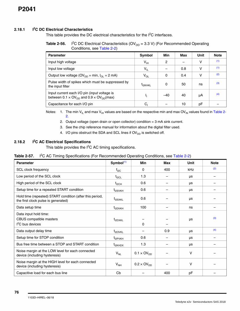
P2041
2.18.1 I2C DC Electrical Characteristics This table provides the DC electrical characteristics for the I2C interfaces.
Notes: 1. The min VIL and max VIH values are based on the respective min and max OVIN values found in Table 2-2.
2. Output voltage (open drain or open collector) condition = 3 mA sink current.
3. See the chip reference manual for information about the digital filter used.
4. I/O pins obstruct the SDA and SCL lines if OVDD is switched off.
2.18.2 I2C AC Electrical Specifications This table provides the I2C AC timing specifications.
Table 2-56. I2C DC Electrical Characteristics (OVDD = 3.3 V) (For Recommended Operating Conditions, see Table 2-2)
Parameter Symbol Min Max Unit Note
Input high voltage VIH 2 – V (1)
Input low voltage VIL – 0.8 V (1)
Output low voltage (OVDD = min, IOL = 2 mA) VOL 0 0.4 V (2)
Pulse width of spikes which must be suppressed by the input filter
tI2KHKL 0 50 ns (3)
Input current each I/O pin (input voltage isbetween 0.1 × OVDD and 0.9 × OVDD(max)
II –40 40 µA (4)
Capacitance for each I/O pin CI – 10 pF –
Table 2-57. I2C AC Timing Specifications (For Recommended Operating Conditions, see Table 2-2)
Parameter Symbol(1) Min Max Unit Note
SCL clock frequency fI2C 0 400 kHz (2)
Low period of the SCL clock tI2CL 1.3 – µs –
High period of the SCL clock tI2CH 0.6 – µs –
Setup time for a repeated START condition tI2SVKH 0.6 – µs –
Hold time (repeated) START condition (after this period, the first clock pulse is generated)
tI2SXKL 0.6 – µs –
Data setup time tI2DVKH 100 – ns –
Data input hold time:
CBUS compatible masters
I2C bus devices
tI2DXKL –
0
–
–
µs (3)
Data output delay time tI2OVKL – 0.9 µs (4)
Setup time for STOP condition tI2PVKH 0.6 – µs –
Bus free time between a STOP and START condition tI2KHDX 1.3 – µs –
Noise margin at the LOW level for each connected device (including hysteresis)
VNL 0.1 × OVDD – V –
Noise margin at the HIGH level for each connected device (including hysteresis)
VNH 0.2 × OVDD – V –
Capacitive load for each bus line Cb – 400 pF –
761103D–HIREL–06/18
Teledyne e2v Semiconductors SAS 2018

P2041
Notes: 1. The symbols used for timing specifications herein follow the pattern t(first two letters of functional block)(signal)(state)(reference)(state) for inputs andt(first two letters of functional block)(reference)(state)(signal)(state) for outputs. For example, tI2DVKH symbolizes I2C timing (I2) with respect to the time data input signals (D) reaching the valid state (V) relative to the tI2C clock reference (K) going to the high (H) state or setup time. Also, tI2SXKL symbolizes I2C timing (I2) for the time that the data with respect to the START condition (S) went invalid (X) relative to the tI2C clock reference (K) going to the low (L) state or hold time. Also, tI2PVKH symbolizes I2C timing (I2) for the time that the data with respect to the STOP condition (P) reaches the valid state (V) relative to the tI2C clock reference (K) going to the high (H) state or setup time.
2. The requirements for I2C frequency calculation must be followed. Refer to Freescale application note AN2919, “Determining the I2C Frequency Divider Ratio for SCL.”
3. As a transmitter, the device provides a delay time of at least 300 ns for the SDA signal (referred to the VIHmin of the SCL signal) to bridge the undefined region of the falling edge of SCL to avoid unintended generation of a START or STOP condition. When the device acts as the I2C bus master while transmitting, it drives both SCL and SDA. As long as the load on SCL and SDA are balanced, the device does not generate an unintended START or STOP condition. Therefore, the 300 ns SDA output delay time is not a concern. If, under some rare condition, the 300 ns SDA output delay time is required for the device as transmitter, application note AN2919 referred to in note 2 above is recommended.
4. The maximum tI2OVKL must be met only if the device does not stretch the LOW period (tI2CL) of the SCL signal.
This figure provides the AC test load for the I2C.
Figure 2-23. I2C AC Test Load
This figure shows the AC timing diagram for the I2C bus.
Figure 2-24. I2C Bus AC Timing Diagram
2.19 GPIO This section describes the DC and AC electrical characteristics for the GPIO interface.
Output Z0 = 50Ω OVDD/2RL = 50Ω
SrS
SDA
SCL
tI2SXKL
tI2CL
tI2CHtI2DXKL,tI2OVKL
tI2DVKH
tI2SXKL
tI2SVKH
tI2KHKL
tI2PVKH
P S
tI2KHDX
771103D–HIREL–06/18
Teledyne e2v Semiconductors SAS 2018

P2041
2.19.1 GPIO DC Electrical Characteristics This table provides the DC electrical characteristics for GPIO pins operating atCVDD, LVDD or OVDD = 3.3 V
Notes: 1. The min VIL and max VIH values are based on the min and max L/OVIN respective values found in Table 2-2.
2. The symbol VIN, in this case, represents the L/OVIN symbol referenced in Section 2.1.2 ”Recommended Operating Conditions” on page 35.
This table provides the DC electrical characteristics for GPIO pins operating at CVDD or LVDD = 2.5 V.
Notes: 1. The min VIL and max VIH values are based on the respective min and max LVIN values found in Table 2-2.
2. The symbol VIN, in this case, represents the LVIN symbol referenced in Section 2.1.2 ”Recommended Operating Conditions” on page 35.
2.19.2 GPIO AC Timing Specifications This table provides the GPIO input and output AC timing specifications.
Table 2-58. GPIO DC Electrical Characteristics (CVDD, LVDD or OVDD = 3.3 V) (For Recommended Operating Conditions, see Table 2-2)
Parameter Symbol Min Max Unit Note
Input high voltage VIH 2.0 – V (1)
Input low voltage VIL – 0.8 V (1)
Input current (OVIN = 0 V or OVIN = OVDD) IIN – ±40 µA (2)
Output high voltage (OVDD = min, IOH = –2 mA) VOH 2.4 – V –
Output low voltage (OVDD = min, IOL = 2 mA) VOL – 0.4 V –
Table 2-59. GPIO DC Electrical Characteristics (CVDD or LVDD = 2.5 V) (For Recommended Operating Conditions, see Table 2-2)
Parameter Symbol Min Max Unit Note
Input high voltage VIH 1.7 – V (1)
Input low voltage VIL – 0.7 V (1)
Input current (VIN = 0 V or VIN = LVDD) IIN – ±40 µA (2)
Output high voltage (LVDD = min, IOH = –2 mA) VOH 2.0 – V –
Output low voltage (LVDD = min, IOH = 2 mA) VOL – 0.4 V –
Table 2-60. GPIO Input AC Timing Specifications (For Recommended Operating Conditions, see Table 2-2)
Parameter Symbol Min Unit Note
GPIO inputs: minimum pulse width tPIWID 20 ns (1)
781103D–HIREL–06/18
Teledyne e2v Semiconductors SAS 2018

P2041
Note: 1. GPIO inputs and outputs are asynchronous to any visible clock. GPIO outputs must be synchronized before use by any external synchronous logic. GPIO inputs are required to be valid for at least tPIWID to ensure proper operation.
This figure provides the AC test load for the GPIO.
Figure 2-25. GPIO AC Test Load
2.20 High-Speed Serial Interfaces (HSSI) The device features a serializer/deserializer (SerDes) interface to be used for high-speed serialinterconnect applications. The SerDes interface can be used for PCI Express, Serial RapidIO, XAUI,Aurora, and SGMII data transfers.
This section describes the common portion of SerDes DC electrical specifications: the DC requirementfor SerDes reference clocks. The SerDes data lane’s transmitter (Tx) and receiver (Rx) reference circuitsare also shown.
2.20.1 Signal Terms Definition The SerDes utilizes differential signaling to transfer data across the serial link. This section defines termsused in the description and specification of differential signals.
This figure shows how the signals are defined. For illustration purposes only, one SerDes lane is used inthe description. This figure shows the waveform for either a transmitter output (SD_TXn and SD_TXn) ora receiver input (SD_RXn and SD_RXn). Each signal swings between A volts and B volts where A > B.
Figure 2-26. Differential Voltage Definitions for Transmitter or Receiver
Using this waveform, the definitions are as shown in the following list. To simplify the illustration, thedefinitions assume that the SerDes transmitter and receiver operate in a fully symmetrical differentialsignaling environment:
Single-Ended SwingThe transmitter output signals and the receiver input signals SD_TXn, SD_TXn, SD_RXn and SD_RXn
Output Z0 = 50Ω OVDD/2
RL = 50Ω
Differential Swing, VID or VOD = A – B
A Volts
B Volts
SD_TXn orSD_RXn
SD_TXnSD_RXn
Differential Peak Voltage, VDIFFp = |A – B|Differential Peak-Peak Voltage, VDIFFpp = 2 VDIFFp (not shown)
Vcm = (A + B)/2
or
791103D–HIREL–06/18
Teledyne e2v Semiconductors SAS 2018

P2041
each have a peak-to-peak swing of A – B volts. This is also referred as each signal wire’s single-endedswing.
Differential Output Voltage, VOD (or Differential Output Swing):The differential output voltage (or swing) of the transmitter, VOD, is defined as the difference of the twocomplimentary output voltages: VSD_TXn – VSD_TXn. The VOD value can be either positive or negative.
Differential Input Voltage, VID (or Differential Input Swing):The differential input voltage (or swing) of the receiver, VID, is defined as the difference of the twocomplimentary input voltages: VSD_RXn – VSD_RXn. The VID value can be either positive or negative.
Differential Peak Voltage, VDIFFp
The peak value of the differential transmitter output signal or the differential receiver input signal isdefined as the differential peak voltage, VDIFFp = |A – B| volts.
Differential Peak-to-Peak, VDIFFp-p
Since the differential output signal of the transmitter and the differential input signal of the receiver eachrange from A – B to –(A – B) volts, the peak-to-peak value of the differential transmitter output signal orthe differential receiver input signal is defined as differential peak-to-peak voltage, VDIFFp-p = 2 × VDIFFp =2 × |(A – B)| volts, which is twice the differential swing in amplitude, or twice of the differential peak. Forexample, the output differential peak-peak voltage can also be calculated as VTX-DIFFp-p = 2 × |VOD|.
Differential WaveformThe differential waveform is constructed by subtracting the inverting signal (SD_TXn, for example) fromthe non-inverting signal (SD_TXn, for example) within a differential pair. There is only one signal tracecurve in a differential waveform. The voltage represented in the differential waveform is not referenced toground. See Figure 2-31 as an example for differential waveform.
Common Mode Voltage, Vcm
The common mode voltage is equal to half of the sum of the voltages between each conductor of abalanced interchange circuit and ground. In this example, for SerDes output, Vcm_out =(VSD_TXn +VSD_TXn)÷ 2 = (A + B) ÷ 2, which is the arithmetic mean of the two complimentary output voltages within adifferential pair. In a system, the common mode voltage may often differ from one component’s output tothe other’s input. It may be different between the receiver input and driver output circuits within the samecomponent. It is also referred to as the DC offset on some occasions.
To illustrate these definitions using real values, consider the example of a current mode logic (CML)transmitter that has a common mode voltage of 2.25 V and outputs, TD and TD. If these outputs have aswing from 2.0 V to 2.5 V, the peak-to-peak voltage swing of each signal (TD or TD) is 500 mV p-p,which is referred to as the single-ended swing for each signal. Because the differential signalingenvironment is fully symmetrical in this example, the transmitter output’s differential swing (VOD) has thesame amplitude as each signal’s single-ended swing. The differential output signal ranges between 500mV and –500 mV. In other words, VOD is 500 mV in one phase and –500 mV in the other phase. Thepeak differential voltage (VDIFFp) is 500 mV.The peak-to-peak differential voltage (VDIFFp-p) is 1000 mV p-p.
2.20.2 SerDes Reference Clocks The SerDes reference clock inputs are applied to an internal PLL whose output creates the clock usedby the corresponding SerDes lanes. The SerDes reference clocks inputs are SD_REF_CLK1 andSD_REF_CLK1 for SerDes bank1 and SD_REF_CLK2 and SD_REF_CLK2 for SerDes bank2.
SerDes banks 1–2 may be used for various combinations of the following IP blocks based on the RCWconfiguration field SRDS_PRTCL:
801103D–HIREL–06/18
Teledyne e2v Semiconductors SAS 2018

P2041
• SerDes bank 1: PCI Express 1/2/3, sRIO1/2, SGMII (1.25 Gbps only).
• SerDes bank 2: PCI Express3, SGMII (1.25 or 3.125 GBaud), SATA or Aurora or XAUI.
The following sections describe the SerDes reference clock requirements and provide applicationinformation.
2.20.2.1 SerDes Reference Clock Receiver Characteristics This figure shows a receiver reference diagram of the SerDes reference clocks.
Figure 2-27. Receiver of SerDes Reference Clocks
The characteristics of the clock signals are as follows:
• The SerDes transceivers core power supply voltage requirements (SVDD) are as specified in Section 2.1.2 ”Recommended Operating Conditions” on page 35.
• The SerDes reference clock receiver reference circuit structure is as follows:
– The SD_REF_CLKn and SD_REF_CLKn are internally AC-coupled differential inputs as shown in Figure 2-27. Each differential clock input (SD_REF_CLKn or SD_REF_CLKn) has on-chip 50- termination to SGND followed by on-chip AC-coupling.
– The external reference clock driver must be able to drive this termination.
– The SerDes reference clock input can be either differential or single-ended. Refer to the differential mode and single-ended mode descriptions below for detailed requirements.
• The maximum average current requirement also determines the common mode voltage range.
– When the SerDes reference clock differential inputs are DC coupled externally with the clock driver chip, the maximum average current allowed for each input pin is 8 mA. In this case, the exact common mode input voltage is not critical as long as it is within the range allowed by the maximum average current of 8 mA because the input is AC-coupled on-chip.
– This current limitation sets the maximum common mode input voltage to be less than 0.4 V (0.4 V ÷ 50 = 8 mA) while the minimum common mode input level is 0.1 V above SGND. For
InputAmp
50Ω
50Ω
SD_REF_CLKn
SD_REF_CLKn
811103D–HIREL–06/18
Teledyne e2v Semiconductors SAS 2018

P2041
example, a clock with a 50/50 duty cycle can be produced by a clock driver with output driven by its current source from 0 mA to 16 mA (0–0.8 V), such that each phase of the differential input has a single-ended swing from 0 V to 800 mV with the common mode voltage at 400 mV.
– If the device driving the SD_REF_CLKn and SD_REF_CLKn inputs cannot drive 50 to SGND DC or the drive strength of the clock driver chip exceeds the maximum input current limitations, it must be AC-coupled off-chip.
• The input amplitude requirement is described in detail in the following sections.
2.20.2.2 DC Level Requirement for SerDes Reference Clocks The DC level requirement for the SerDes reference clock inputs is different depending on the signalingmode used to connect the clock driver chip and SerDes reference clock inputs, as described below:
• Differential Mode
– The input amplitude of the differential clock must be between 400 mV and 1600 mV differential peak-peak (or between 200 mV and 800 mV differential peak). In other words, each signal wire of the differential pair must have a single-ended swing of less than 800 mV and greater than 200 mV. This requirement is the same for both external DC-coupled or AC-coupled connection.
– For an external DC-coupled connection, as described in Section 2.20.2.1 ”SerDes Reference Clock Receiver Characteristics” on page 81, the maximum average current requirements sets the requirement for average voltage (common mode voltage) as between 100 mV and 400 mV. This figure shows the SerDes reference clock input requirement for DC-coupled connection scheme.
Figure 2-28. Differential Reference Clock Input DC Requirements (External DC-Coupled)
– For an external AC-coupled connection, there is no common mode voltage requirement for the clock driver. Because the external AC-coupling capacitor blocks the DC level, the clock driver and the SerDes reference clock receiver operate in different common mode voltages. The SerDes reference clock receiver in this connection scheme has its common mode voltage set to SGND. Each signal wire of the differential inputs is allowed to swing below and above the common mode voltage (SGND). This figure shows the SerDes reference clock input requirement for AC-coupled connection scheme.
SD_REF_CLKn
SD_REF_CLKn
Vmax < 800 mV
Vmin > 0 V
100 mV < Vcm < 400 mV
200 mV < Input Amplitude or Differential Peak < 800 mV
821103D–HIREL–06/18
Teledyne e2v Semiconductors SAS 2018

P2041
Figure 2-29. Differential Reference Clock Input DC Requirements (External AC-Coupled)
• Single-Ended Mode
– The reference clock can also be single-ended. The SD_REF_CLKn input amplitude (single-ended swing) must be between 400 mV and 800 mV peak-peak (from VMIN to VMAX) with SD_REF_CLKn either left unconnected or tied to ground.
– The SD_REF_CLKn input average voltage must be between 200 and 400 mV. Figure 2-30 shows the SerDes reference clock input requirement for single-ended signaling mode.
– To meet the input amplitude requirement, the reference clock inputs may need to be DC- or AC-coupled externally. For the best noise performance, the reference of the clock could be DC- or AC-coupled into the unused phase (SD_REF_CLKn) through the same source impedance as the clock input (SD_REF_CLKn) in use.
Figure 2-30. Single-Ended Reference Clock Input DC Requirements
SD_REF_CLKn
SD_REF_CLKn
Vcm
200 mV < Input Amplitude or Differential Peak < 800 mV
Vmax ≤ Vcm + 400 mV
Vmin > Vcm – 400 mV
SD_REF_CLKn
SD_REF_CLKn
400 mV ≤ SD_REF_CLKn Input Amplitude ≤ 800 mV
0 V
831103D–HIREL–06/18
Teledyne e2v Semiconductors SAS 2018
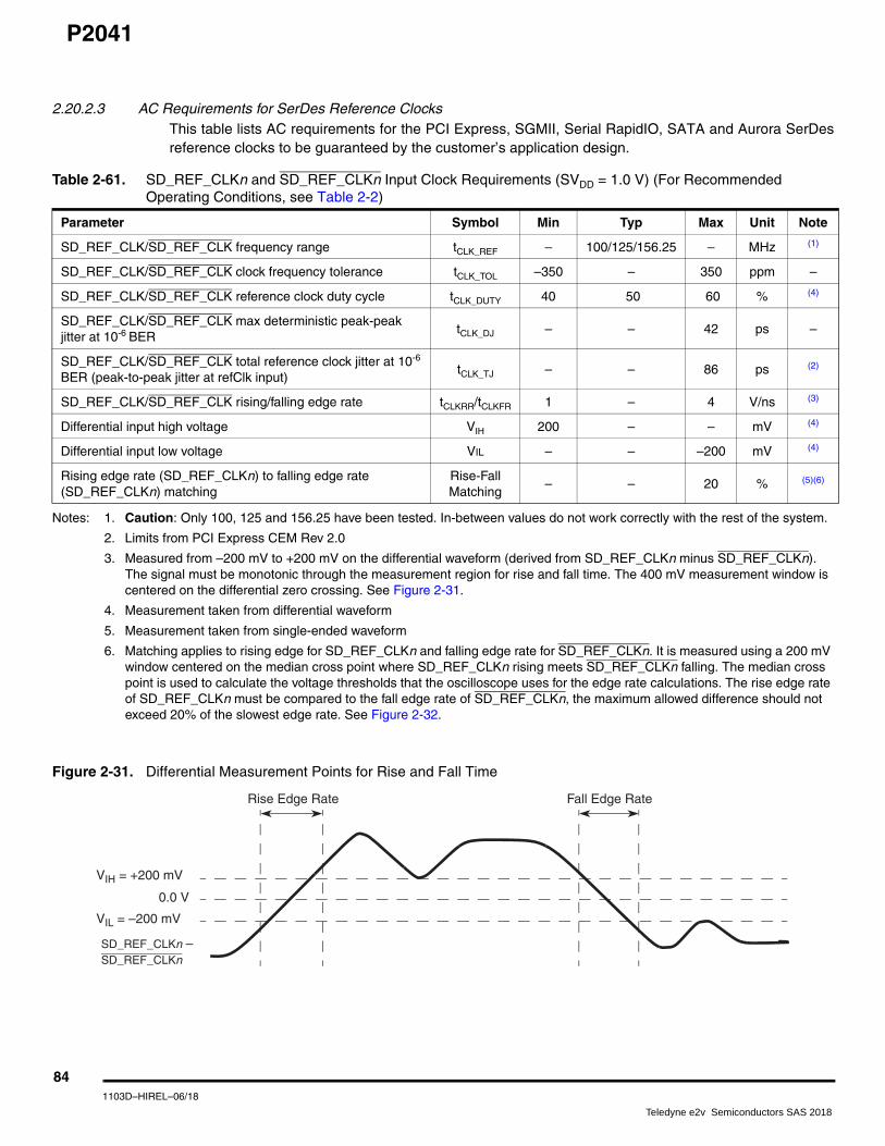
P2041
2.20.2.3 AC Requirements for SerDes Reference Clocks This table lists AC requirements for the PCI Express, SGMII, Serial RapidIO, SATA and Aurora SerDesreference clocks to be guaranteed by the customer’s application design.
Notes: 1. Caution: Only 100, 125 and 156.25 have been tested. In-between values do not work correctly with the rest of the system.
2. Limits from PCI Express CEM Rev 2.0
3. Measured from –200 mV to +200 mV on the differential waveform (derived from SD_REF_CLKn minus SD_REF_CLKn). The signal must be monotonic through the measurement region for rise and fall time. The 400 mV measurement window is centered on the differential zero crossing. See Figure 2-31.
4. Measurement taken from differential waveform
5. Measurement taken from single-ended waveform
6. Matching applies to rising edge for SD_REF_CLKn and falling edge rate for SD_REF_CLKn. It is measured using a 200 mV window centered on the median cross point where SD_REF_CLKn rising meets SD_REF_CLKn falling. The median cross point is used to calculate the voltage thresholds that the oscilloscope uses for the edge rate calculations. The rise edge rate of SD_REF_CLKn must be compared to the fall edge rate of SD_REF_CLKn, the maximum allowed difference should not exceed 20% of the slowest edge rate. See Figure 2-32.
Figure 2-31. Differential Measurement Points for Rise and Fall Time
Table 2-61. SD_REF_CLKn and SD_REF_CLKn Input Clock Requirements (SVDD = 1.0 V) (For Recommended Operating Conditions, see Table 2-2)
Parameter Symbol Min Typ Max Unit Note
SD_REF_CLK/SD_REF_CLK frequency range tCLK_REF – 100/125/156.25 – MHz (1)
SD_REF_CLK/SD_REF_CLK clock frequency tolerance tCLK_TOL –350 – 350 ppm –
SD_REF_CLK/SD_REF_CLK reference clock duty cycle tCLK_DUTY 40 50 60 % (4)
SD_REF_CLK/SD_REF_CLK max deterministic peak-peakjitter at 10-6 BER
tCLK_DJ – – 42 ps –
SD_REF_CLK/SD_REF_CLK total reference clock jitter at 10-6
BER (peak-to-peak jitter at refClk input) tCLK_TJ – – 86 ps (2)
SD_REF_CLK/SD_REF_CLK rising/falling edge rate tCLKRR/tCLKFR 1 – 4 V/ns (3)
Differential input high voltage VIH 200 – – mV (4)
Differential input low voltage VIL – – –200 mV (4)
Rising edge rate (SD_REF_CLKn) to falling edge rate(SD_REF_CLKn) matching
Rise-Fall Matching
– – 20 % (5)(6)
VIH = +200 mV
VIL = –200 mV
0.0 V
SD_REF_CLKn – SD_REF_CLKn
Fall Edge RateRise Edge Rate
841103D–HIREL–06/18
Teledyne e2v Semiconductors SAS 2018

P2041
Figure 2-32. Single-Ended Measurement Points for Rise and Fall Time Matching
2.20.2.4 Spread Spectrum Clock SD_REF_CLK1/SD_REF_CLK1 were designed to work with a spread spectrum clock (+0 to 0.5%spreading at 30–33 kHz rate is allowed), assuming both ends have same reference clock. For betterresults, a source without significant unintended modulation must be used.
SD_REF_CLK2/SD_REF_CLK2 were designed to work with a spread spectrum clock (+0 to 0.5%spreading at 30–33 kHz rate is allowed), assuming both ends have same reference clock and theindustry protocol specifications supports it. For better results, a source without significant unintendedmodulation must be used.
2.20.3 SerDes Transmitter and Receiver Reference Circuits This figure shows the reference circuits for SerDes data lane’s transmitter and receiver.
Figure 2-33. SerDes Transmitter and Receiver Reference Circuits
The DC and AC specification of SerDes data lanes are defined in each interface protocol section belowbased on the application usage:
• Section 2.20.4 ”PCI Express” on page 86
• Section 2.20.5 ”Serial RapidIO (sRIO)” on page 93
• Section 2.20.6 ”XAUI” on page 97
• Section 2.20.7 ”Aurora” on page 99
• Section 2.20.8 ”Serial ATA (SATA)” on page 101
• Section 2.20.9 ”SGMII Interface” on page 105
VCROSS MEDIAN
VCROSS MEDIAN - 100 mV
VCROSS MEDIAN + 100 mV
VCROSS MEDIAN
TFALL TRISESDn_REF_CLK
50Ω
50ΩReceiverTransmitter
SD_TXn
SD_TXn SD_RXn
SD_RXn
50Ω
50Ω
851103D–HIREL–06/18
Teledyne e2v Semiconductors SAS 2018
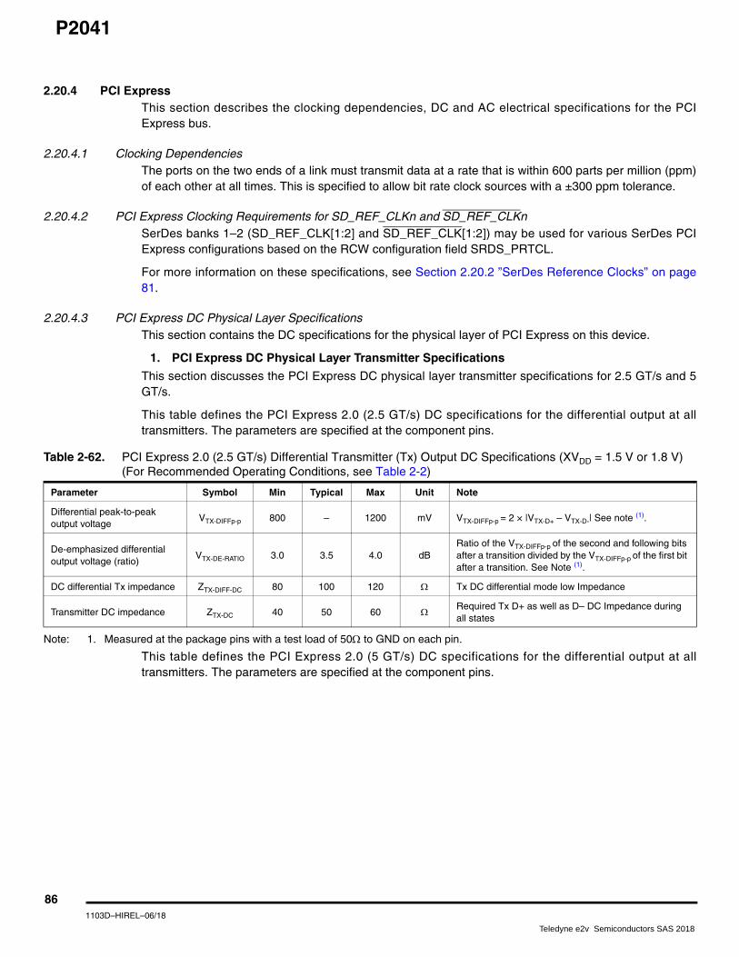
P2041
2.20.4 PCI Express This section describes the clocking dependencies, DC and AC electrical specifications for the PCIExpress bus.
2.20.4.1 Clocking Dependencies The ports on the two ends of a link must transmit data at a rate that is within 600 parts per million (ppm)of each other at all times. This is specified to allow bit rate clock sources with a ±300 ppm tolerance.
2.20.4.2 PCI Express Clocking Requirements for SD_REF_CLKn and SD_REF_CLKn SerDes banks 1–2 (SD_REF_CLK[1:2] and SD_REF_CLK[1:2]) may be used for various SerDes PCIExpress configurations based on the RCW configuration field SRDS_PRTCL.
For more information on these specifications, see Section 2.20.2 ”SerDes Reference Clocks” on page81.
2.20.4.3 PCI Express DC Physical Layer Specifications This section contains the DC specifications for the physical layer of PCI Express on this device.
1. PCI Express DC Physical Layer Transmitter Specifications
This section discusses the PCI Express DC physical layer transmitter specifications for 2.5 GT/s and 5GT/s.
This table defines the PCI Express 2.0 (2.5 GT/s) DC specifications for the differential output at alltransmitters. The parameters are specified at the component pins.
Note: 1. Measured at the package pins with a test load of 50 to GND on each pin.
This table defines the PCI Express 2.0 (5 GT/s) DC specifications for the differential output at alltransmitters. The parameters are specified at the component pins.
Table 2-62. PCI Express 2.0 (2.5 GT/s) Differential Transmitter (Tx) Output DC Specifications (XVDD = 1.5 V or 1.8 V) (For Recommended Operating Conditions, see Table 2-2)
Parameter Symbol Min Typical Max Unit Note
Differential peak-to-peak output voltage
VTX-DIFFp-p 800 – 1200 mV VTX-DIFFp-p = 2 × |VTX-D+ – VTX-D-| See note (1).
De-emphasized differential output voltage (ratio)
VTX-DE-RATIO 3.0 3.5 4.0 dB Ratio of the VTX-DIFFp-p of the second and following bits after a transition divided by the VTX-DIFFp-p of the first bit after a transition. See Note (1).
DC differential Tx impedance ZTX-DIFF-DC 80 100 120 Tx DC differential mode low Impedance
Transmitter DC impedance ZTX-DC 40 50 60 Required Tx D+ as well as D– DC Impedance during all states
861103D–HIREL–06/18
Teledyne e2v Semiconductors SAS 2018

P2041
Note: 1. Measured at the package pins with a test load of 50 to GND on each pin.
2.20.4.4 PCI Express DC Physical Layer Receiver Specifications This section discusses the PCI Express DC physical layer receiver specifications 2.5 GT/s, and 5 GT/s.
This table defines the DC specifications for the PCI Express 2.0 (2.5 GT/s) differential input at allreceivers. The parameters are specified at the component pins.
Notes: 1. Measured at the package pins with a test load of 50 to GND on each pin.
2. Impedance during all LTSSM states. When transitioning from a fundamental reset to detect (the initial state of the LTSSM) there is a 5 ms transition time before receiver termination values must be met on all unconfigured lanes of a port.
3. The Rx DC common mode impedance that exists when no power is present or fundamental reset is asserted. This helps ensure that the receiver detect circuit does not falsely assume a receiver is powered on when it is not. This term must be measured at 300 mV above the Rx ground.
Table 2-63. PCI Express 2.0 (5 GT/s) Differential Transmitter (Tx) Output DC Specifications (XVDD = 1.5 V or 1.8 V) (For Recommended Operating Conditions, see Table 2-2)
Parameter Symbol Min Typical Max Unit Note
Differential peak-to-peak output voltage
VTX-DIFFp-p 800 – 1200 mV VTX-DIFFp-p = 2 × |VTX-D+ – VTX-D-| See Note (1).
Low power differential peak-to-peak output voltage
VTX-DIFFp-p _low 400 500 1200 mV VTX-DIFFp-p = 2 × |VTX-D+ – VTX-D-| See Note (1).
De-emphasized differential output voltage (ratio)
VTX-DE-RATIO-3.5dB 3.0 3.5 4.0 dB Ratio of the VTX-DIFFp-p of the second and following bits after a transition divided by the VTX-DIFFp-p of the first bit after a transition. See Note (1).
De-emphasized differential output voltage (ratio)
VTX-DE-RATIO-6.0dB 5.5 6.0 6.5 dB Ratio of the VTX-DIFFp-p of the second and following bits after a transition divided by the VTX-DIFFp-p of the first bit after a transition. See Note (1).
DC differential Tx impedance ZTX-DIFF-DC 80 100 120 Tx DC differential mode low impedance
Transmitter DC Impedance ZTX-DC 40 50 60 Required Tx D+ as well as D– DC impedance during all states
Table 2-64. PCI Express 2.0 (2.5 GT/s) Differential Receiver (Rx) Input DC Specifications (XVDD = 1.5 V or 1.8 V) (For Recommended Operating Conditions, see Table 2-2)
Parameter Symbol Min Typical Max Unit Note
Differential input peak-to-peak voltage
VRX-DIFFp-p 120 – 1200 mV VRX-DIFFp-p = 2 × |VRX-D+ – VRX-D-| Note (1).
DC differential input impedance
ZRX-DIFF-DC 80 100 120 Rx DC differential mode impedance. See Note (2)
DC input impedance ZRX-DC 40 50 60 Required Rx D+ as well as D– DC Impedance (50 ±20% tolerance). See Notes (1) and (2).
Powered down DC input impedance
ZRX-HIGH-IMP-DC 50 k – –
Required Rx D+ as well as D– DC Impedance when the receiver terminations do not have power. See Note (3).
Electrical idle detect threshold
VRX-IDLE-DET-DIFFp-p 65 – 175 mV VRX-IDLE-DET-DIFFp-p = 2 × |VRX-D+ – VRX-D–| Measured at the package pins of the receiver
871103D–HIREL–06/18
Teledyne e2v Semiconductors SAS 2018

P2041
This table defines the DC specifications for the PCI Express 2.0 (5 GT/s) differential input at allreceivers. The parameters are specified at the component pins.
Notes: 1. Measured at the package pins with a test load of 50 to GND on each pin.
2. Impedance during all LTSSM states. When transitioning from a fundamental reset to detect (the initial state of the LTSSM) there is a 5 ms transition time before receiver termination values must be met on all unconfigured lanes of a port.
3. The Rx DC common mode impedance that exists when no power is present or fundamental reset is asserted. This helps ensure that the receiver detect circuit does not falsely assume a receiver is powered on when it is not. This term must be measured at 300 mV above the Rx ground.
2.20.4.5 PCI Express AC Physical Layer Specifications This section contains the DC specifications for the physical layer of PCI Express on this device.
1. PCI Express AC Physical Layer Transmitter Specifications
This section discusses the PCI Express AC physical layer transmitter specifications 2.5 GT/s and5 GT/s.
Table 2-65. PCI Express 2.0 (5 GT/s) Differential Receiver (Rx) Input DC Specifications (XVDD = 1.5 V or 1.8 V) (For Recommended Operating Conditions, see Table 2-2)
Parameter Symbol Min Typical Max Unit Note
Differential input peak-to-peak voltage
VRX-DIFFp-p 120 – 1200 V VRX-DIFFp-p = 2 × |VRX-D+ – VRX-D–| See Note (1).
DC differential input impedance ZRX-DIFF-DC 80 100 120 Rx DC Differential mode impedance. See Note (2)
DC input impedance ZRX-DC 40 50 60 Required Rx D+ as well as D– DC Impedance (50 ±20% tolerance). See Notes (1) and (2).
Powered down DC input impedance
ZRX-HIGH-IMP-DC 50 – – kRequired Rx D+ as well as D– DC Impedance when the Receiver terminations do not have power. See Note (3).
Electrical idle detect threshold VRX-IDLE-DET-DIFFp-p 65 – 175 mV VRX-IDLE-DET-DIFFp-p = 2 × |VRX-D+ –VRX-D–| Measured at the package pins of the receiver
881103D–HIREL–06/18
Teledyne e2v Semiconductors SAS 2018

P2041
This table defines the PCI Express 2.0 (2.5 GT/s) AC specifications for the differential output at alltransmitters. The parameters are specified at the component pins. The AC timing specifications do notinclude RefClk jitter.
Notes: 1. No test load is necessarily associated with this value.
2. Specified at the measurement point into a timing and voltage test load as shown in Figure 2-34 and measured over any 250 consecutive Tx UIs.
3. A TTX-EYE = 0.75 UI provides for a total sum of deterministic and random jitter budget of TTX-JITTER-MAX = 0.25 UI for the transmitter collected over any 250 consecutive Tx UIs. The TTX-EYE-MEDIAN-to-MAX-JITTER median is less than half of the total Tx jitter budget collected over any 250 consecutive Tx UIs. It must be noted that the median is not the same as the mean. The jitter median describes the point in time where the number of jitter points on either side is approximately equal as opposed to the averaged time value.
4. The chip’s SerDes transmitter does not have CTX built-in. An external AC coupling capacitor is required.
Table 2-66. PCI Express 2.0 (2.5 GT/s) Differential Transmitter (Tx) Output AC Specifications (For Recommended Operating Conditions, see Table 2-2)
Parameter Symbol Min Typical Max Unit Note
Unit interval UI 399.88 400 400.12 ps Each UI is 400 ps ± 300 ppm. UI does not account for spread spectrum clock dictated variations. See note (1).
Minimum Tx eye width TTX-EYE 0.75 – – UI
The maximum transmitter jitter can be derived asTTX-MAX-JITTER = 1 – TTX-EYE = 0.25 UI. Does not include spread spectrum or RefCLK jitter. Includes device random jitter at 10-12. See notes (2) and (3).
Maximum time between the jitter median and maximum deviation from the median
TTX-EYE-MEDIAN
to-MAX-JITTER– – 0.125 UI
Jitter is defined as the measurement variation of the crossing points (VTX-DIFFp-p = 0 V) in relation to a recovered Tx UI. A recovered Tx UI is calculated over 3500 consecutive unit intervals of sample data. Jitter is measured using all edges of the 250 consecutive UI in the center of the 3500 UI used for calculating the Tx UI. See notes (2) and (3).
AC coupling capacitor CTX 75 – 200 nF All transmitters must be AC coupled. The AC coupling is required either within the media or within the transmitting component itself. See note (4).
891103D–HIREL–06/18
Teledyne e2v Semiconductors SAS 2018
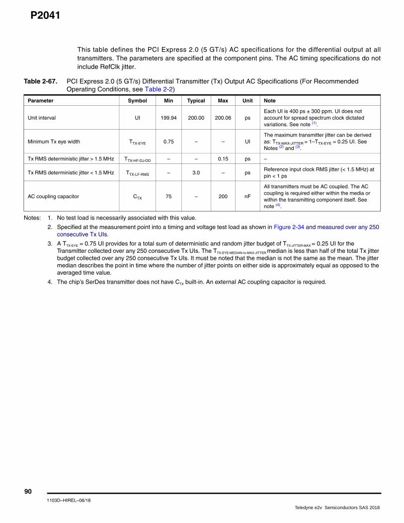
P2041
This table defines the PCI Express 2.0 (5 GT/s) AC specifications for the differential output at alltransmitters. The parameters are specified at the component pins. The AC timing specifications do notinclude RefClk jitter.
Notes: 1. No test load is necessarily associated with this value.
2. Specified at the measurement point into a timing and voltage test load as shown in Figure 2-34 and measured over any 250 consecutive Tx UIs.
3. A TTX-EYE = 0.75 UI provides for a total sum of deterministic and random jitter budget of TTX-JITTER-MAX = 0.25 UI for the Transmitter collected over any 250 consecutive Tx UIs. The TTX-EYE-MEDIAN-to-MAX-JITTER median is less than half of the total Tx jitter budget collected over any 250 consecutive Tx UIs. It must be noted that the median is not the same as the mean. The jitter median describes the point in time where the number of jitter points on either side is approximately equal as opposed to the averaged time value.
4. The chip’s SerDes transmitter does not have CTX built-in. An external AC coupling capacitor is required.
Table 2-67. PCI Express 2.0 (5 GT/s) Differential Transmitter (Tx) Output AC Specifications (For Recommended Operating Conditions, see Table 2-2)
Parameter Symbol Min Typical Max Unit Note
Unit interval UI 199.94 200.00 200.06 ps Each UI is 400 ps ± 300 ppm. UI does not account for spread spectrum clock dictated variations. See note (1).
Minimum Tx eye width TTX-EYE 0.75 – – UI The maximum transmitter jitter can be derived as: TTX-MAX-JITTER = 1–TTX-EYE = 0.25 UI. See Notes (2) and (3).
Tx RMS deterministic jitter > 1.5 MHz TTX-HF-DJ-DD – – 0.15 ps –
Tx RMS deterministic jitter < 1.5 MHz TTX-LF-RMS – 3.0 – ps Reference input clock RMS jitter (< 1.5 MHz) at pin < 1 ps
AC coupling capacitor CTX 75 – 200 nF
All transmitters must be AC coupled. The AC coupling is required either within the media or within the transmitting component itself. See note (4).
901103D–HIREL–06/18
Teledyne e2v Semiconductors SAS 2018

P2041
2. PCI Express AC Physical Layer Receiver Specifications
This section discusses the PCI Express AC physical layer receiver specifications 2.5 GT/s and 5 GT/s.
This table defines the AC specifications for the PCI Express 2.0 (2.5 GT/s) differential input at allreceivers. The parameters are specified at the component pins. The AC timing specifications do notinclude RefClk jitter.
Notes: 1. No test load is necessarily associated with this value.
2. Specified at the measurement point and measured over any 250 consecutive UIs. The test load in Figure 2-34 must be used as the Rx device when taking measurements. If the clocks to the Rx and Tx are not derived from the same reference clock, the Tx UI recovered from 3500 consecutive UI must be used as a reference for the eye diagram.
3. A TRX-EYE = 0.40 UI provides for a total sum of 0.60 UI deterministic and random jitter budget for the transmitter and interconnect collected any 250 consecutive UIs. The TRX-EYE-MEDIAN-to-MAX-JITTER specification ensures a jitter distribution in which the median and the maximum deviation from the median is less than half of the total. UI jitter budget collected over any 250 consecutive Tx UIs. It must be noted that the median is not the same as the mean. The jitter median describes the point in time where the number of jitter points on either side is approximately equal as opposed to the averaged time value. If the clocks to the Rx and Tx are not derived from the same reference clock, the Tx UI recovered from 3500 consecutive UI must be used as the reference for the eye diagram.
4. It is recommended that the recovered Tx UI is calculated using all edges in the 3500 consecutive UI interval with a fit algorithm using a minimization merit function. Least squares and median deviation fits have worked well with experimental and simulated data.
Table 2-68. PCI Express 2.0 (2.5 GT/s) Differential Receiver (Rx) Input AC Specifications (For Recommended Operating Conditions, see Table 2-2)
Parameter Symbol Min Typical Max Unit Note
Unit Interval UI 399.88 400.00 400.12 ps Each UI is 400 ps ± 300 ppm. UI does not account for spread spectrum clock dictated variations. See note (1).
Minimum receiver eye width TRX-EYE 0.4 – – UI
The maximum interconnect media and Transmitter jitter that can be tolerated by the Receiver can be derived as TRX-MAX-JITTER = 1 – TRX-EYE = 0.6 UI. See Notes (2) and (3).
Maximum time between the jitter median and maximum deviation from the median.
TRX-EYE-MEDIAN -
to-MAX-JITTER – – 0.3 UI
Jitter is defined as the measurement variation of the crossing points (VRX-DIFFp-p = 0 V) in relation to a recovered Tx UI. A recovered Tx UI is calculated over 3500 consecutive unit intervals of sample data. Jitter is measured using all edges of the 250 consecutive UI in the center of the 3500 UI used for calculating the Tx UI. See Notes (2) (3) and (4).
911103D–HIREL–06/18
Teledyne e2v Semiconductors SAS 2018
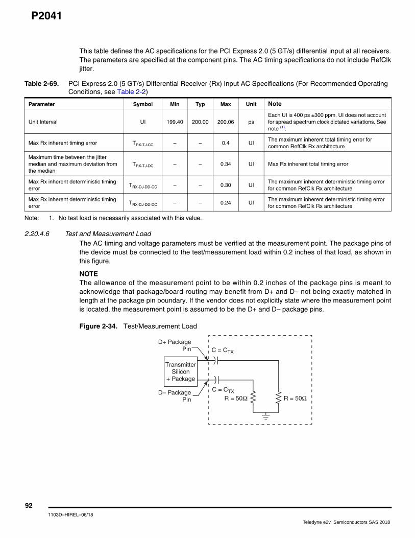
P2041
This table defines the AC specifications for the PCI Express 2.0 (5 GT/s) differential input at all receivers.The parameters are specified at the component pins. The AC timing specifications do not include RefClkjitter.
Note: 1. No test load is necessarily associated with this value.
2.20.4.6 Test and Measurement Load The AC timing and voltage parameters must be verified at the measurement point. The package pins ofthe device must be connected to the test/measurement load within 0.2 inches of that load, as shown inthis figure.
NOTE The allowance of the measurement point to be within 0.2 inches of the package pins is meant toacknowledge that package/board routing may benefit from D+ and D– not being exactly matched inlength at the package pin boundary. If the vendor does not explicitly state where the measurement pointis located, the measurement point is assumed to be the D+ and D– package pins.
Figure 2-34. Test/Measurement Load
Table 2-69. PCI Express 2.0 (5 GT/s) Differential Receiver (Rx) Input AC Specifications (For Recommended Operating Conditions, see Table 2-2)
Parameter Symbol Min Typ Max Unit Note
Unit Interval UI 199.40 200.00 200.06 ps Each UI is 400 ps ±300 ppm. UI does not account for spread spectrum clock dictated variations. See note (1).
Max Rx inherent timing error TRX-TJ-CC – – 0.4 UI The maximum inherent total timing error for common RefClk Rx architecture
Maximum time between the jitter median and maximum deviation from the median
TRX-TJ-DC – – 0.34 UI Max Rx inherent total timing error
Max Rx inherent deterministic timing error
TRX-DJ-DD-CC – – 0.30 UI The maximum inherent deterministic timing error for common RefClk Rx architecture
Max Rx inherent deterministic timing error
TRX-DJ-DD-DC – – 0.24 UI The maximum inherent deterministic timing error for common RefClk Rx architecture
TransmitterSilicon
+ Package
D+ PackagePin
D– PackagePin
C = CTX
C = CTX
R = 50ΩR = 50Ω
921103D–HIREL–06/18
Teledyne e2v Semiconductors SAS 2018

P2041
2.20.5 Serial RapidIO (sRIO) This section describes the DC and AC electrical specifications for the Serial RapidIO interface of the LP-Serial physical layer. The electrical specifications cover both single and multiple-lane links. Twotransmitters (short run and long run) and a single receiver are specified for each of three baud rates:2.50, 3.125, and 5 GBaud.
Two transmitter specifications allow for solutions ranging from simple board-to-board interconnect todriving two connectors across a backplane. A single receiver specification is given that accepts signalsfrom both the short run and long run transmitter specifications.
The short run transmitter must be used mainly for chip-to-chip connections on either the same printedcircuit board or across a single connector. This covers the case where connections are made to amezzanine (daughter) card. The minimum swings of the short run specification reduce the overall powerused by the transceivers.
The long run transmitter specifications use larger voltage swings that are capable of driving signalsacross backplanes. This allows a user to drive signals across two connectors and a backplane.The specifications allow a distance of at least 50 cm at all baud rates.
All unit intervals are specified with a tolerance of ±100 ppm. The worst case frequency differencebetween any transmit and receive clock is 200 ppm.
To ensure interoperability between drivers and receivers of different vendors and technologies, ACcoupling at the receiver input must be used.
2.20.5.1 Signal Definitions This section defines the terms used in the description and specification of the differential signals used bythe LP-Serial links. This figure shows how the signals are defined. The figures show waveforms for eithera transmitter output (TD and TD) or a receiver input (RD and RD). Each signal swings between A voltsand B volts where A > B. Using these waveforms, the definitions are as follows:
• The transmitter output signals and the receiver input signals: TD, TD, RD, and RD: each have a peak-to-peak swing of A – B volts.
• The differential output signal of the transmitter, VOD, is defined as VTD – VTD
• The differential input signal of the receiver, VID, is defined as VRD – VRD
• The differential output signal of the transmitter and the differential input signal of the receiver each range from A – B to –(A – B) volts
• The peak value of the differential transmitter output signal and the differential receiver input signal is A – B volts.
• The peak-to-peak value of the differential transmitter output signal and the differential receiver input signal is 2 × (A – B) volts.
931103D–HIREL–06/18
Teledyne e2v Semiconductors SAS 2018

P2041
Figure 2-35. Differential Peak-Peak Voltage of Transmitter or Receiver
To illustrate these definitions using real values, consider the case of a CML (current mode logic)transmitter that has a common mode voltage of 2.25 V, and each of its outputs, TD and TD, has a swingthat goes between 2.5 V and 2.0 V. Using these values, the peak-to-peak voltage swing of the signalsTD and TD is 500 mV p-p. The differential output signal ranges between 500 mV and –500 mV. Thepeak differential voltage is 500 mV. The peak-to-peak differential voltage is 1000 mV p-p.
2.20.5.2 Equalization With the use of high-speed serial links, the interconnect media causes degradation of the signal at thereceiver and produces effects such as inter-symbol interference (ISI) or data-dependent jitter. This losscan be large enough to degrade the eye opening at the receiver beyond what is allowed in thespecification. To negate a portion of these effects, equalization can be used. The most commonequalization techniques that can be used are as follows:
• Pre-emphasis on the transmitter
• A passive high-pass filter network placed at the receiver, often referred to as passive equalization.
• The use of active circuits in the receiver, often referred to as adaptive equalization.
2.20.5.3 Serial RapidIO Clocking Requirements for SD_REF_CLKn and SD_REF_CLKn SerDes bank 1 (SD_REF_CLK1 and SD_REF_CLK1) may be used for various SerDes Serial RapidIOconfigurations based on the RCW configuration field SRDS_PRTCL. Serial RapidIO is not supported onSerDes banks 2.
For more information on these specifications, see Section 2.20.2 ”SerDes Reference Clocks” on page81.
2.20.5.4 DC Requirements for Serial RapidIO This section explains the DC requirements for the Serial RapidIO interface.
1. DC Serial RapidIO Timing Transmitter Specifications
LP-Serial transmitter electrical and timing specifications are stated in the text and tables of thissection. The differential return loss, S11, of the transmitter in each case is better than the following:
–10 dB for (Baud Frequency) ÷ 10 < Freq(f) < 625 MHz
–10 dB + 10log(f ÷ 625 MHz) dB for 625 MHz Freq(f) Baud Frequency
The reference impedance for the differential return loss measurements is 100 resistive. Differentialreturn loss includes contributions from on-chip circuitry, chip packaging, and any off-chipcomponents related to the driver. The output impedance requirement applies to all valid outputlevels.
Differential Peak-Peak = 2 (A – B)
A VoltsTD or RD
TD or RDB Volts
941103D–HIREL–06/18
Teledyne e2v Semiconductors SAS 2018

P2041
It is recommended that the 20%–80% rise/fall time of the transmitter, as measured at the transmitteroutput, have a minimum value 60 ps in each case.
It is recommended that the timing skew at the output of an LP-Serial transmitter between the twosignals that comprise a differential pair not exceed 20 ps at 2.50 GBaud and 15 ps at 3.125 GBaudand XX ps at 5 GBaud.
This table defines the transmitter DC specifications for Serial RapidIO operating at XVDD = 1.5 V or1.8 V.
Note: 1. Voltage relative to COMMON of either signal comprising a differential pair.
2. DC Serial RapidIO Receiver Specifications
LP-Serial receiver electrical and timing specifications are stated in the text and tables of this section.
Receiver input impedance results in a differential return loss better than 10 dB and a common modereturn loss better than 6 dB from 100 MHz to (0.8) × (Baud Frequency). This includes contributionsfrom on-chip circuitry, the chip package, and any off-chip components related to the receiver. ACcoupling components are included in this requirement. The reference impedance for return lossmeasurements is 100 resistive for differential return loss and 25 resistive for common mode.
This table defines the receiver DC specifications for Serial RapidIO operating at XVDD = 1.5 V or1.8 V.
Note: 1. Measured at the receiver.
Table 2-70. Serial RapidIO Transmitter DC Timing Specifications: 2.5 GBaud, 3.125 GBaud, 5 GBaud (For Recommended Operating Conditions, see Table 2-2)
Parameter Symbol Min Typ Max Unit Note
Output voltage VO –0.40 – 2.30 V (1)
Long-run differential output voltage VDIFFPP 800 – 1600 mV p-p –
Short-run differential output voltage VDIFFPP 500 – 1000 mV p-p –
Table 2-71. Serial RapidIO Receiver DC Timing Specifications: 2.5 GBaud, 3.125 GBaud, 5 GBaud (For Recommended Operating Conditions, see Table 2-2)
Parameter Symbol Min Typ Max Unit Note
Differential input voltage VIN 200 – 1600 mV p-p (1)
951103D–HIREL–06/18
Teledyne e2v Semiconductors SAS 2018

P2041
2.20.5.5 AC Requirements for Serial RapidIO This section explains the AC requirements for the Serial RapidIO interface.
1. AC Requirements for Serial RapidIO Transmitter
This table defines the transmitter AC specifications for the Serial RapidIO interface. The AC timingspecifications do not include RefClk jitter.
This table defines the receiver AC specifications for Serial RapidIO. The AC timing specifications do notinclude RefClk jitter.
Notes: 1. Measured at receiver
2. Total jitter is composed of three components: deterministic jitter, random jitter, and single frequency sinusoidal jitter. The sinusoidal jitter may have any amplitude and frequency in the unshaded region of Figure 2-36. The sinusoidal jitter component is included to ensure margin for low-frequency jitter, wander, noise, crosstalk, and other variable system effects.
Table 2-72. Serial RapidIO Transmitter AC Timing Specifications (For Recommended Operating Conditions, see Table 2-2)
Parameter Symbol Min Typical Max Unit
Deterministic jitter JD – – 0.17 UI p-p
Total jitter JT – – 0.35 UI p-p
Unit interval: 2.5 GBaud UI 400 – 100 ppm 400 400 + 100 ppm ps
Unit interval: 3.125 GBaud UI 320 – 100 ppm 320 320 + 100 ppm ps
Table 2-73. Serial RapidIO Receiver AC Timing Specifications (For Recommended Operating Conditions, see Table 2-2)
Parameter Symbol Min Typical Max Unit Note
Deterministic jitter tolerance JD 0.37 – – UI p-p (1)
Combined deterministic and random jitter tolerance
JDR 0.55 – – UI p-p (1)
Total jitter tolerance2 JT 0.65 – – UI p-p (1)
Bit error rate BER – – 10–12 – –
Unit interval: 2.5 GBaud UI 400 – 100 ppm 400 400 + 100 ppm ps –
Unit interval: 3.125 GBaud UI 320 – 100 ppm 320 320 + 100 ppm ps –
961103D–HIREL–06/18
Teledyne e2v Semiconductors SAS 2018

P2041
Figure 2-36. Single-Frequency Sinusoidal Jitter Limits
2.20.6 XAUI This section describes the DC and AC electrical specifications for the XAUI bus.
2.20.6.1 XAUI DC Electrical Characteristics This section discusses the XAUI DC electrical characteristics for the clocking signals, transmitter, andreceiver.
1. DC Requirements for XAUI SD_REF_CLKn and SD_REF_CLKn
Only SerDes banks 2-3 (SD_REF_CLK[2:3] and SD_REF_CLK[2:3]) may be used for variousSerDes XAUI configurations based on the RCW Configuration field SRDS_PRTCL. XAUI is notsupported on SerDes bank 1.
For more information on these specifications, see Section 2.20.2.2 ”DC Level Requirement for Ser-Des Reference Clocks” on page 82.
2. XAUI Transmitter DC Electrical Characteristics
This table defines the XAUI transmitter DC electrical characteristics.
Note: 1. Absolute output voltage limit
8.5 UI p-p
0.10 UI p-p
Sinusoidal
Jitter
Amplitude
22.1 kHz 1.875 MHz 20 MHzFrequency
Table 2-74. XAUI Transmitter DC Electrical Characteristics (XVDD = 1.5 V or 1.8 V) (For Recommended Operating Conditions, see Table 2-2)
Parameter Symbol Min Typical Max Unit Note
Output voltage VO –0.40 – 2.30 V (1)
Differential output voltage VDIFFPP 800 – 1600 mV p-p –
971103D–HIREL–06/18
Teledyne e2v Semiconductors SAS 2018

P2041
3. XAUI Receiver DC Electrical Characteristics
This table defines the XAUI receiver DC electrical characteristics.
Note: 1. Measured at the receiver.
2.20.6.2 XAUI AC Timing Specifications This section discusses the XAUI AC timing specifications for the clocking signals, transmitter, andreceiver.
1. AC Requirements for XAUI SD_REF_CLKn and SD_REF_CLKn
This table specifies AC requirements for SD_REF_CLKn and SD_REF_CLKn, where n = [2:3]. OnlySerDes banks 2-3 may be used for various SerDes XAUI configurations based on the RCWConfiguration field SRDS_PRTCL. XAUI is not supported on SerDes bank 1.
Notes: 1. Measured from –200 mV to +200 mV on the differential waveform (derived from SD_REF_CLKn minus SD_REF_CLKn). The signal must be monotonic through the measurement region for rise and fall time. The 400 mV measurement window is centered on the differential zero crossing. See Figure 2-31.
2. Measurement taken from differential waveform
3. Measurement taken from single-ended waveform
4. Matching applies to rising edge for SD_REF_CLKn and falling edge rate for SD_REF_CLKn. It is measured using a 200 mV window centered on the median cross point where SD_REF_CLKn rising meets SD_REF_CLKn falling. The median cross point is used to calculate the voltage thresholds that the oscilloscope uses for the edge rate calculations. The rise edge rate of SD_REF_CLKn must be compared to the fall edge rate of SD_REF_CLKn, the maximum allowed difference should not exceed 20% of the slowest edge rate. See Figure 2-32.
Table 2-75. XAUI Receiver DC Timing Specifications (XVDD = 1.5 V or 1.8 V) (For Recommended Operating Conditions, see Table 2-2)
Parameter Symbol Min Typical Max Unit Note
Differential input voltage VIN 200 900 1600 mV p-p (1)
Table 2-76. XAUI AC SD_REF_CLKn and SD_REF_CLKn Input Clock Requirements (SVDD = 1.0 V) (For Recommended Operating Conditions, see Table 2-2)
Parameter Symbol Min Typical Max Unit Note
SD_REF_CLK/SD_REF_CLK frequency range tCLK_REF – 125/ 156.25 – MHz –
SD_REF_CLK/SD_REF_CLK clock frequency tolerance tCLK_TOL –100 – +100 ppm –
SD_REF_CLK/SD_REF_CLK reference clock duty cycle (measured at 1.6 V)
tCLK_DUTY 40 50 60 % –
SD_REF_CLK/SD_REF_CLK cycle to cycle jitter (period jitter at refClk input)
tCLK_CJ – – 100 ps –
SD_REF_CLK/SD_REF_CLK total reference clock jitter (peak-to-peak phase jitter at refClk input)
tCLK_PJ –50 – 50 ps –
SD_REF_CLK/SD_REF_CLK rising/falling edge rate tCLKRR/tCLKFR 1 – 4 V/ns 1
Differential input high voltage VIH 200 – – mV 2
Differential input low voltage VIL – – –200 mV 2
Rising edge rate (SD_REF_CLKn) to falling edge rate (SD_REF_CLKn) matching
Rise-Fall Matching
– – 20 % 3, 4
981103D–HIREL–06/18
Teledyne e2v Semiconductors SAS 2018

P2041
2. XAUI Transmitter AC Timing Specifications
This table defines the XAUI transmitter AC timing specifications. RefClk jitter is not included.
3. XAUI Receiver AC Timing Specifications
This table defines the receiver AC specifications for XAUI. RefClk jitter is not included.
Notes: 1. Measured at receiver
2. Total jitter is composed of three components: deterministic jitter, random jitter, and single frequency sinusoidal jitter. The sinusoidal jitter may have any amplitude and frequency in the unshaded region of Figure 2-36. The sinusoidal jitter component is included to ensure margin for low frequency jitter, wander, noise, crosstalk, and other variable system effects.
2.20.7 Aurora This section describes the Aurora clocking requirements and AC and DC electrical characteristics.
2.20.7.1 Aurora DC Electrical Characteristics This section describes the DC electrical characteristics for Aurora.
1. Aurora DC Clocking Requirements for SD_REF_CLKn and SD_REF_CLKn
Only SerDes bank 2(SD_REF_CLK2 and SD_REF_CLK2) may be used for SerDes Auroraconfigurations based on the RCW configuration field SRDS_PRTCL. Aurora is not supported onSerDes banks 1.
For more information on these specifications, see Section 2.20.2 ”SerDes Reference Clocks” onpage 81.
Table 2-77. XAUI Transmitter AC Timing Specifications (For Recommended Operating Conditions, see Table 2-2)
Parameter Symbol Min Typical Max Unit Note
Deterministic jitter JD – – 0.17 UI p-p –
Total jitter JT – – 0.35 UI p-p –
Unit Interval: 3.125 GBaud UI 320 – 100 ppm 320 320 + 100 ppm ps –
Table 2-78. XAUI Receiver AC Timing Specifications (For Recommended Operating Conditions, see Table 2-2)
Parameter Symbol Min Typical Max Unit Note
Deterministic jitter tolerance JD 0.37 – – UI p-p (1)
Combined deterministic and random jitter tolerance
JDR 0.55 – – UI p-p (1)
Total jitter tolerance JT 0.65 – – UI p-p (1)(2)
Bit error rate BER – – 10–12 – –
Unit Interval: 3.125 GBaud UI 320 – 100 ppm 320 320 + 100 ppm ps –
991103D–HIREL–06/18
Teledyne e2v Semiconductors SAS 2018

P2041
2. Aurora Transmitter DC Electrical Characteristics
This table provides the Aurora transmitter DC electrical characteristics (XVDD = 1.5 V or 1.8 V).
3. Aurora Receiver DC Electrical Characteristics
This table provides the Aurora receiver DC electrical characteristics (XVDD = 1.5 V or 1.8 V).
Note: 1. Measured at receiver.
2.20.7.2 Aurora AC Timing Specifications This section describes the AC timing specifications for Aurora.
1. Aurora AC Clocking Requirements for SD_REF_CLKn and SD_REF_CLKn
Only SerDes bank 2(SD_REF_CLK2 and SD_REF_CLK2) may be used for SerDes Auroraconfigurations based on the RCW configuration field SRDS_PRTCL. Aurora is not supported onSerDes banks 1.
2. Aurora Transmitter AC Timing Specifications
This table defines the Aurora transmitter AC timing specifications. RefClk jitter is not included.
Table 2-79. Aurora Transmitter DC Electrical Characteristics (XVDD = 1.5 V or 1.8 V) (For Recommended Operating Conditions, see Table 2-2)
Parameter Symbol Min Typical Max Unit
Differential output voltage VDIFFPP 800 – 1600 mV p-p
Table 2-80. Aurora Receiver DC Electrical Characteristics (XVDD = 1.5 V or 1.8 V) (For Recommended Operating Conditions, see Table 2-2)
Parameter Symbol Min Typical Max Unit Note
Differential input voltage VIN 120 900 1200 mV p-p (1)
Table 2-81. Aurora Transmitter AC Timing Specifications (For Recommended Operating Conditions, see Table 2-2)
Parameter Symbol Min Typical Max Unit
Deterministic jitter JD – – 0.17 UI p-p
Total jitter JT – – 0.35 UI p-p
Unit Interval: 2.5 GBaud UI 400 – 100 ppm 400 400 + 100 ppm ps
Unit Interval: 3.125 GBaud UI 320 – 100 ppm 320 320 + 100 ppm ps
Unit Interval: 5.0 GBaud UI 200 – 100 ppm 200 200 + 100 ppm ps
1001103D–HIREL–06/18
Teledyne e2v Semiconductors SAS 2018
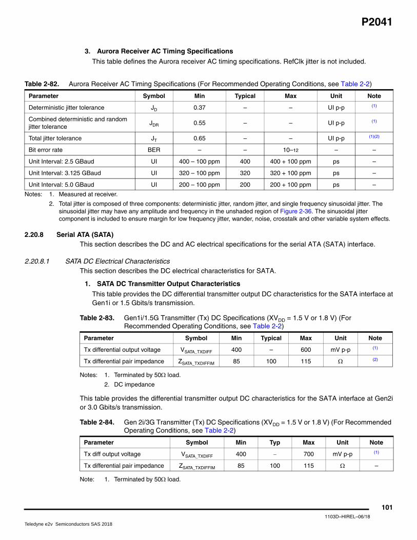
P2041
3. Aurora Receiver AC Timing Specifications
This table defines the Aurora receiver AC timing specifications. RefClk jitter is not included.
Notes: 1. Measured at receiver.
2. Total jitter is composed of three components: deterministic jitter, random jitter, and single frequency sinusoidal jitter. The sinusoidal jitter may have any amplitude and frequency in the unshaded region of Figure 2-36. The sinusoidal jitter component is included to ensure margin for low frequency jitter, wander, noise, crosstalk and other variable system effects.
2.20.8 Serial ATA (SATA) This section describes the DC and AC electrical specifications for the serial ATA (SATA) interface.
2.20.8.1 SATA DC Electrical Characteristics This section describes the DC electrical characteristics for SATA.
1. SATA DC Transmitter Output Characteristics
This table provides the DC differential transmitter output DC characteristics for the SATA interface atGen1i or 1.5 Gbits/s transmission.
Notes: 1. Terminated by 50 load.
2. DC impedance
This table provides the differential transmitter output DC characteristics for the SATA interface at Gen2ior 3.0 Gbits/s transmission.
Note: 1. Terminated by 50 load.
Table 2-82. Aurora Receiver AC Timing Specifications (For Recommended Operating Conditions, see Table 2-2)
Parameter Symbol Min Typical Max Unit Note
Deterministic jitter tolerance JD 0.37 – – UI p-p (1)
Combined deterministic and random jitter tolerance
JDR 0.55 – – UI p-p (1)
Total jitter tolerance JT 0.65 – – UI p-p (1)(2)
Bit error rate BER – – 10–12 – –
Unit Interval: 2.5 GBaud UI 400 – 100 ppm 400 400 + 100 ppm ps –
Unit Interval: 3.125 GBaud UI 320 – 100 ppm 320 320 + 100 ppm ps –
Unit Interval: 5.0 GBaud UI 200 – 100 ppm 200 200 + 100 ppm ps –
Table 2-83. Gen1i/1.5G Transmitter (Tx) DC Specifications (XVDD = 1.5 V or 1.8 V) (For Recommended Operating Conditions, see Table 2-2)
Parameter Symbol Min Typical Max Unit Note
Tx differential output voltage VSATA_TXDIFF 400 – 600 mV p-p (1)
Tx differential pair impedance ZSATA_TXDIFFIM 85 100 115 (2)
Table 2-84. Gen 2i/3G Transmitter (Tx) DC Specifications (XVDD = 1.5 V or 1.8 V) (For Recommended Operating Conditions, see Table 2-2)
Parameter Symbol Min Typ Max Unit Note
Tx diff output voltage VSATA_TXDIFF 400 – 700 mV p-p (1)
Tx differential pair impedance ZSATA_TXDIFFIM 85 100 115 –
1011103D–HIREL–06/18
Teledyne e2v Semiconductors SAS 2018

P2041
2. SATA DC Receiver (Rx) Input Characteristics
This table provides the Gen1i or 1.5 Gbits/s differential receiver input DC characteristics for theSATA interface.
Note: 1. Voltage relative to common of either signal comprising a differential pair
This table provides the Gen2i or 3 Gbits/s differential receiver input DC characteristics for the SATAinterface.
Notes: 1. Voltage relative to common of either signal comprising a differential pair
2. DC impedance
Table 2-85. Gen1i/1.5 G Receiver (Rx) Input DC Specifications (XVDD = 1.5 V or 1.8 V) (For Recommended Operating Conditions, see Table 2-2)
Parameter Symbol Min Typical Max Unit Note
Differential input voltage VSATA_RXDIFF 240 – 600 mV p-p (1)
Differential Rx input impedance ZSATA_RXSEIM 85 100 115 –
OOB signal detection threshold VSATA_OOB 50 120 240 mV p-p –
Table 2-86. Gen2i/3 G Receiver (Rx) Input DC Specifications (XVDD = 1.5 V or 1.8 V) (For Recommended Operating Conditions, see Table 2-2)
Parameter Symbol Min Typical Max Unit Note
Differential input voltage VSATA_RXDIFF 275 – 750 mV p-p (1)
Differential Rx input impedance ZSATA_RXSEIM 85 100 115 (2)
OOB signal detection threshold VSATA_OOB 75 120 240 mV p-p (2)
1021103D–HIREL–06/18
Teledyne e2v Semiconductors SAS 2018

P2041
2.20.8.2 SATA AC Timing Specifications This section discusses the SATA AC timing specifications.
1. AC Requirements for SATA REF_CLK
The AC requirements for the SATA reference clock are listed in this table to be guaranteed by thecustomer’s application design.
Notes: 1. Caution: Only 100, 125 MHz have been tested. In-between values do not work correctly with the rest of the system.
2. At RefClk input
3. In a frequency band from 150 kHz to 15 MHz at BER of 10-12
4. Total peak-to-peak deterministic jitter must be less than or equal to 50 ps.
This figure shows the reference clock timing waveform.
Figure 2-37. Reference Clock Timing Waveform
Table 2-87. SATA Reference Clock Input Requirements (For Recommended Operating Conditions, see Table 2-2)
Parameter Symbol Min Typ Max Unit Note
SD_REF_CLK/SD_REF_CLK frequency range tCLK_REF – 100/125 – MHz (1)
SD_REF_CLK/SD_REF_CLK clock frequency tolerance tCLK_TOL –350 – +350 ppm –
SD_REF_CLK/SD_REF_CLK reference clock duty cycle (measured at 1.6 V)
tCLK_DUTY 40 50 60 % –
SD_REF_CLK/SD_REF_CLK cycle-to-cycle clock jitter (period jitter)
tCLK_CJ – – 100 ps (2)
SD_REF_CLK/SD_REF_CLK total reference clock jitter, phase jitter (peak-peak)
tCLK_PJ –50 – +50 ps (2)(3)(4)
TH
TL
Ref_CLK
1031103D–HIREL–06/18
Teledyne e2v Semiconductors SAS 2018

P2041
2.20.8.3 AC Transmitter Output Characteristics This table provides the differential transmitter output AC characteristics for the SATA interface at Gen1ior 1.5 Gbits/s transmission. The AC timing specifications do not include RefClk jitter.
Note: 1. Measured at Tx output pins peak to peak phase variation, random data pattern
This table provides the differential transmitter output AC characteristics for the SATA interface at Gen2ior 3.0 Gbits/s transmission. The AC timing specifications do not include RefClk jitter.
Note: 1. Measured at Tx output pins peak-to-peak phase variation, random data pattern
2.20.8.4 AC Differential Receiver Input Characteristics This table provides the Gen1i or 1.5 Gbits/s differential receiver input AC characteristics for the SATAinterface. The AC timing specifications do not include RefClk jitter.
Note: 1. Measured at receiver.
Table 2-88. Gen1i/1.5 G Transmitter (Tx) AC Specifications (For Recommended Operating Conditions, see Table 2-2)
Parameter Symbol Min Typ Max Unit Note
Channel speed tCH_SPEED – 1.5 – Gbps –
Unit Interval TUI 666.4333 666.6667 670.2333 ps –
Total jitter data-data 5 UI USATA_TXTJ5UI – – 0.355 UI p-p (1)
Total jitter, data-data 250 UI USATA_TXTJ250UI – – 0.47 UI p-p (1)
Deterministic jitter, data-data 5 UI USATA_TXDJ5UI – – 0.175 UI p-p (1)
Deterministic jitter, data-data 250 UI USATA_TXDJ250UI – – 0.22 UI p-p (1)
Table 2-89. Gen 2i/3 G Transmitter (Tx) AC Specifications (For Recommended Operating Conditions, see Table 2-2)
Parameter Symbol Min Typ Max Unit Note
Channel speed tCH_SPEED – 3.0 – Gbps –
Unit Interval TUI 333.2167 333.3333 335.1167 ps –
Total jitter fC3dB = fBAUD ÷ 10 USATA_TXTJfB/10 – – 0.3 UI p-p (1)
Total jitter fC3dB = fBAUD ÷ 500 USATA_TXTJfB/500 – – 0.37 UI p-p (1)
Total jitter fC3dB = fBAUD ÷ 1667 USATA_TXTJfB/1667 – – 0.55 UI p-p (1)
Deterministic jitter, fC3dB = fBAUD ÷ 10 USATA_TXDJfB/10 – – 0.17 UI p-p (1)
Deterministic jitter, fC3dB = fBAUD ÷ 500 USATA_TXDJfB/500 – – 0.19 UI p-p (1)
Deterministic jitter, fC3dB = fBAUD ÷ 1667 USATA_TXDJfB/1667 – – 0.35 UI p-p (1)
Table 2-90. Gen 1i/1.5G Receiver (Rx) AC Specifications (For Recommended Operating Conditions, see Table 2-2)
Parameter Symbol Min Typical Max Unit Note
Unit Interval TUI 666.4333 666.6667 670.2333 ps –
Total jitter data-data 5 UI USATA_TXTJ5UI – – 0.43 UI p-p (1)
Total jitter, data-data 250 UI USATA_TXTJ250UI – – 0.60 UI p-p (1)
Deterministic jitter, data-data 5 UI USATA_TXDJ5UI – – 0.25 UI p-p (1)
Deterministic jitter, data-data 250 UI USATA_TXDJ250UI – – 0.35 UI p-p (1)
1041103D–HIREL–06/18
Teledyne e2v Semiconductors SAS 2018

P2041
This table provides the differential receiver input AC characteristics for the SATA interface at Gen2i or3.0 Gbits/s transmission. The AC timing specifications do not include RefClk jitter.
Note: 1. Measured at receiver.
2.20.9 SGMII Interface Each SGMII port features a 4-wire AC-coupled serial link from the SerDes interface of the device, asshown in Figure 2-38, where CTX is the external (on board) AC-coupled capacitor. Each output pin ofthe SerDes transmitter differential pair features 50 output impedance. Each input of the SerDesreceiver differential pair features 50 on-die termination to XGND. The reference circuit of the SerDestransmitter and receiver is shown in Figure 2-33.
1. SGMII Clocking Requirements for SD_REF_CLKn and SD_REF_CLKn
When operating in SGMII mode, the EC_GTX_CLK125 clock is not required for this port. Instead, aSerDes reference clock is required on SD_REF_CLK[1:2] and SD_REF_CLK[1:2] pins. SerDesbanks 1–2 may be used for SerDes SGMII configurations based on the RCW Configuration fieldSRDS_PRTCL.
For more information on these specifications, see Section 2.20.2 ”SerDes Reference Clocks” onpage 81.
Table 2-91. Gen 2i/3G Receiver (Rx) AC Specifications (For Recommended Operating Conditions, see Table 2-2)
Parameter Symbol Min Typical Max Unit Note
Unit Interval TUI 333.2167 333.3333 335.1167 ps –
Total jitter fC3dB =fBAUD ÷ 10 USATA_TXTJfB/10 – – 0.46 UI p-p (1)
Total jitter fC3dB =fBAUD ÷ 500 USATA_TXTJfB/500 – – 0.60 UI p-p (1)
Total jitter fC3dB =fBAUD ÷ 1667 USATA_TXTJfB/1667 – – 0.65 UI p-p (1)
Deterministic jitter, fC3dB =fBAUD ÷ 10 USATA_TXDJfB/10 – – 0.35 UI p-p (1)
Deterministic jitter, fC3dB =fBAUD ÷ 500 USATA_TXDJfB/500 – – 0.42 UI p-p (1)
Deterministic jitter, fC3dB =fBAUD ÷ 1667 USATA_TXDJfB/1667 – – 0.35 UI p-p (1)
1051103D–HIREL–06/18
Teledyne e2v Semiconductors SAS 2018

P2041
2.20.9.1 SGMII DC Electrical Characteristics This section discusses the electrical characteristics for the SGMII interface.
1. SGMII Transmit DC Timing Specifications
This table describe the SGMII SerDes transmitter and receiver AC-coupled DC electricalcharacteristics for 1.25 GBaud. Transmitter DC characteristics are measured at the transmitteroutputs (SD_TXn and SD_TXn) as shown in Figure 2-39.
Notes: 1. This does not align to DC-coupled SGMII.
2. |VOD| = |VSD_TXn – VSD_TXn|. |VOD| is also referred to as output differential peak voltage. VTX-DIFFp-p = 2*|VOD|.
3. Example amplitude reduction setting for SGMII on SerDes bank 1 lane E: B1TECRE0[AMP_RED] = 0b000010 for an output differential voltage of 459 mV typical.
4. The |VOD| value shown in the Typ column is based on the condition of XVDD_SRDSn-Typ = 1.5 V or 1.8 V, no common mode offset variation. SerDes transmitter is terminated with 100 differential load between SD_TXn and SD_TXn.
Table 2-92. SGMII DC Transmitter Electrical Characteristics (XVDD = 1.5 V or 1.8 V) (For Recommended Operating Conditions, see Table 2-2)
Parameter Symbol Min Typ Max Unit Note
Output high voltage VOH – – 1.5 x |VOD|-max mV (1)
Output low voltage VOL |VOD|-min/2 – – mV (1)
Output differential voltage(2)(3)(4) (XVDD-Typ at 1.5 V and 1.8 V)
|VOD| 320 500.0 725.0 mV B(1-2)TECR(lane)0[AMP_RED]
=0b000000
293.8 459.0 665.6 B(1-2)TECR(lane)0[AMP_RED]
=0b000010
266.9 417.0 604.7 B(1-2)TECR(lane)0[AMP_RED]
=0b000101
240.6 376.0 545.2 B(1-2)TECR(lane)0[AMP_RED]
=0b001000
213.1 333.0 482.9 B(1-2)TECR(lane)0[AMP_RED]
=0b001100
186.9 292.0 423.4 B(1-2)TECR(lane)0[AMP_RED]
=0b001111
160.0 250.0 362.5 B(1-2)TECR(lane)0[AMP_RED]
=0b010011
Output impedance (single-ended) RO 40 50 60 –
1061103D–HIREL–06/18
Teledyne e2v Semiconductors SAS 2018

P2041
Figure 2-38. 4-Wire AC-Coupled SGMII Serial Link Connection Example
Figure 2-39. SGMII Transmitter DC Measurement Circuit
This table defines the SGMII 2.5x transmitter DC electrical characteristics for 3.125 GBaud.
Note: 1. Absolute output voltage limit
Table 2-93. SGMII 2.5x Transmitter DC Electrical Characteristics (XVDD = 1.5 V or 1.8 V) (For Recommended Operating Conditions, see Table 2-2)
Parameter Symbol Min Typical Max Unit Note
Output voltage VO –0.40 – 2.30 V (1)
Differential output voltage VDIFFPP 800 – 1600 mV p-p –
SGMIISerDes Interface
50Ω
50Ω Transmitter
SD_TXn SD_RX
SD_TXn SD_RXn
Receiver
CTX
CTX
50Ω
50Ω
SD_RXn
SD_RXn
Receiver Transmitter
SD_TXn
SD_TXn
CTX
CTX
50Ω
50Ω
50Ω
50Ω
50Ω
Transmitter
SD_TXn
SD_TXn50Ω
VOD
SGMIISerDes Interface
50Ω
50Ω
1071103D–HIREL–06/18
Teledyne e2v Semiconductors SAS 2018

P2041
2. SGMII DC Receiver Electrical Characteristics
This table lists the SGMII DC receiver electrical characteristics for 1.25 GBaud. Source synchronousclocking is not supported. Clock is recovered from the data.
Notes: 1. Input must be externally AC coupled.
2. VRX_DIFFp-p is also referred to as peak-to-peak input differential voltage.
3. The concept of this parameter is equivalent to the electrical idle detect threshold parameter in PCI Express. Refer to Section 2.20.4.4 ”PCI Express DC Physical Layer Receiver Specifications” on page 87 and Section “PCI Express AC Physical Layer Receiver Specifications” on page 91, for further explanation.
4. The REIDL_CTL shown in the table refers to the chip’s SerDes control register B(1–3)GCR(lane)1[REIDL_CTL] bit field.
This table defines the SGMII 2.5x receiver DC electrical characteristics for 3.125 GBaud.
Note: 1. Measured at the receiver.
2.20.9.2 SGMII AC Timing Specifications This section discusses the AC timing specifications for the SGMII interface.
1. SGMII Transmit AC Timing Specifications
This table provides the SGMII transmit AC timing specifications. A source synchronous clock is notsupported. The AC timing specifications do not include RefClk jitter.
Notes: 1. See Figure 2-36 for single frequency sinusoidal jitter measurements.
2. The external AC coupling capacitor is required. It is recommended that it be placed near the device transmitter outputs.
Table 2-94. SGMII DC Receiver Electrical Characteristics (XVDD = 1.5 V or 1.8 V) (For Recommended Operating Conditions, see Table 2-2)
Parameter Symbol Min Typ Max Unit Note
DC Input voltage range – N/A – (1)
Input differential voltage REIDL_CTL = 001xx
VRX_DIFFp-p
100 –1200 mV (2)(4)
REIDL_CTL = 100xx 175 –
Loss of signal threshold
REIDL_CTL = 001xx VLOS
30 – 100 mV (3)(4)
REIDL_CTL = 100xx 65 – 175
Receiver differential input impedance ZRX_DIFF 80 – 120 –
Table 2-95. SGMII 2.5x receiver DC Timing Specifications (XVDD = 1.5 V or 1.8 V) (For Recommended Operating Conditions, see Table 2-2)
Parameter Symbol Min Typical Max Unit Note
Differential input voltage VIN 200 900 1600 mV p-p (1)
Table 2-96. SGMII Transmit AC Timing Specifications (For Recommended Operating Conditions, see Table 2-2)
Parameter Symbol Min Typ Max Unit Note
Deterministic jitter JD – – 0.17 UI p-p –
Total jitter JT – – 0.35 UI p-p (1)
Unit interval: 1.25 GBaud UI 800 – 100 ppm 800 800 + 100 ppm ps –
Unit interval: 3.125 GBaud UI 320 – 100 ppm 320 320 + 100 ppm ps –
AC coupling capacitor CTX 10 200 nF (2)
1081103D–HIREL–06/18
Teledyne e2v Semiconductors SAS 2018

P2041
2. SGMII AC Measurement Details
Transmitter and receiver AC characteristics are measured at the transmitter outputs (SD_TXn andSD_TXn) or at the receiver inputs (SD_RXn and SD_RXn) respectively, as depicted in this figure.
Figure 2-40. SGMII AC Test/Measurement Load
3. SGMII Receiver AC Timing Specification
This table provides the SGMII receiver AC timing specifications. The AC timing specifications do notinclude RefClk jitter. Source synchronous clocking is not supported. Clock is recovered from thedata.
Notes: 1. Measured at receiver
2. Refer to RapidIO™ 1×/4× LP Serial Physical Layer Specification for interpretation of jitter specifications.
3. Total jitter is composed of three components: deterministic jitter, random jitter, and single frequency sinusoidal jitter. The sinusoidal jitter may have any amplitude and frequency in the unshaded region of Figure 2-36. The sinusoidal jitter component is included to ensure margin for low frequency jitter, wander, noise, crosstalk and other variable system effects.
The sinusoidal jitter in the total jitter tolerance may have any amplitude and frequency in the unshadedregion of Figure 2-36.
TransmitterSilicon
+ Package
C = CTX
C = CTX
R = 50Ω R = 50Ω
D+ PackagePin
D– PackagePin
D+ PackagePin
Table 2-97. SGMII Receive AC Timing Specifications (For Recommended Operating Conditions, see Table 2-2)
Parameter Symbol Min Typ Max Unit Note
Deterministic jitter tolerance JD 0.37 – – UI p-p (1)(3)
Combined deterministic and random jitter tolerance JDR 0.55 – – UI p-p (1)(2)
Total jitter tolerance JT 0.65 – – UI p-p (1)(2)(3)
Bit error ratio BER – – 10-12 – –
Unit Interval: 1.25 GBaud UI 800 – 100 ppm 800 800 + 100 ppm ps (1)
Unit Interval: 3.125 GBaud UI 320 – 100 ppm 320 320 + 100 ppm ps (1)
1091103D–HIREL–06/18
Teledyne e2v Semiconductors SAS 2018

P2041
3. Hardware Design Considerations This section discusses the hardware design considerations.
3.1 System Clocking This section describes the PLL configuration of the device. This device includes six PLLs, as follows:
• There are two selectable core cluster PLLs that generate a core clock from the externally supplied SYSCLK input. Core complex 0–1 and platform can select from CC1 PLL; core complex 2–3 can select from CC2 PLL. The frequency ratio between the core cluster PLLs and SYSCLK is selected using the configuration bits as described in Section 3.1.3 ”e500mc Core Cluster to SYSCLK PLL Ratio” on page 111. The frequency for each core complex 0–3 is selected using the configuration bits as described in Table 3-4.
• The platform PLL generates the platform clock from the externally supplied SYSCLK input. The frequency ratio between the platform and SYSCLK is selected using the platform PLL ratio configuration bits as described in Section 3.1.2 ”Platform to SYSCLK PLL Ratio” on page 111.
• The DDR block PLL generates the DDR clock from the externally supplied SYSCLK input (asynchronous mode) or from the platform clock (synchronous mode). The frequency ratio is selected using the Memory Controller Complex PLL multiplier/ratio configuration bits as described in Section 3.1.5 ”DDR Controller PLL Ratios” on page 113.
• Each of the three SerDes blocks has a PLL which generate a core clock from their respective externally supplied SD_REF_CLKn/SD_REF_CLKn inputs. The frequency ratio is selected using the SerDes PLL ratio configuration bits as described in Section 3.1.6 ”Frequency Options” on page 114.
3.1.1 Clock RangesThis table provides the clocking specifications for the processor core, platform, memory, and local bus.
Notes: 1. Caution: The platform clock to SYSCLK ratio and e500-mc core to SYSCLK ratio settings must be chosen such that the resulting SYSCLK frequency, e500mc (core) frequency, and platform clock frequency do not exceed their respective maximum or minimum operating frequencies.
2. The memory bus clock speed is half the DDR3/DDR3L data rate. DDR3 memory bus clock frequency is limited to min = 400 MHz.
3. The local bus clock speed on LCLK[0:1] is determined by the platform clock divided by the local bus ratio programmed in LCRR[CLKDIV]. See the chip reference manual for more information.
Table 3-1. Processor Clocking Specifications
Parameter
Maximum Processor Core Frequency
Unit Notes
1200 MHz 1333 MHz 1500 MHz
Min Max Min Max Min Max
e500mc core PLL frequency 800 1200 800 1333 800 1500 MHz (1)(4)
e500mc core frequency 400 1200 400 1333 400 1500 MHz (4)
Platform clock frequency 600 600 600 667 600 750 MHz (1)
Memory bus clock frequency 400 600 400 667 400 667 MHz (1)(2)(5)(6)
Local bus clock frequency – 83 – 83 – 83 MHz (3)
PME – 300 – 333 – 375 MHz (7)
FMan – 500 – 541 – 583 MHz –
1101103D–HIREL–06/18
Teledyne e2v Semiconductors SAS 2018

P2041
4. The e500mc core can run at e500mc core complex PLL/1 or PLL/2. With a minimum core complex PLL frequency of 800 MHz, this results in a minimum allowable e500mc core frequency of 400 MHz for PLL/2.
5. In synchronous mode, the memory bus clock speed is half the platform clock frequency. In other words, the DDR data rate is the same as the platform frequency. If the desired DDR data rate is higher than the platform frequency, asynchronous mode must be used.
6. In asynchronous mode, the memory bus clock speed is dictated by its own PLL.
7. The PME runs synchronously to the platform clock, running at a frequency of platform clock/2.
8. Core frequency must be at least as fast as the platform frequency.
3.1.2 Platform to SYSCLK PLL Ratio This table shows the allowed platform clock-to-SYSCLK ratios.
The chip platform clock frequency is always below 666 MHz frequencies; set the RCW configuration fieldSYS_PLL_CFG = 0b01.
3.1.3 e500mc Core Cluster to SYSCLK PLL Ratio The clock ratio between SYSCLK and each of the two core cluster PLLs is determined at power up bythe binary value of the RCW field CCn_PLL_RAT. This table describes the supported ratios. Note that acore cluster PLL frequency targeting 1 GHz and above must set RCW field CCn_PLL_CFG = 0b00 forfrequency targeting below 1 GHz set CCn_PLL_CFG = 0b01.
Table 3-2. Platform to SYSCLK PLL Ratios
Binary Value of SYS_PLL_RAT Platform: SYSCLK Ratio
0_0100 4:1
0_0101 5:1
0_0110 6:1
0_0111 7:1
0_1000 8:1
0_1001 9:1
0_1010 10:1
All Others Reserved
1111103D–HIREL–06/18
Teledyne e2v Semiconductors SAS 2018

P2041
This table lists the supported Core Cluster to SYSCLK ratios.
3.1.4 e500mc Core Complex PLL Select The clock frequency of each the e500mc core 0–3 complex is determined by the binary value of theRCW field CCn_PLL_SEL. These tables describe the supported ratios for each core complex 0–3,where each individual core complex can select a frequency from the table.
Table 3-3. e500mc Core Cluster PLL to SYSCLK Ratios
Binary Value of CCn_PLL_RAT Core Cluster: SYSCLK Ratio
0_1000 8:1
0_1001 9:1
0_1010 10:1
0_1011 11:1
0_1100 12:1
0_1101 13:1
0_1110 14:1
0_1111 15:1
1_0000 16:1
1_0001 17:1
1_0010 18:1
All Others Reserved
Table 3-4. e500mc Core Complex [0,1] PLL Select
Binary Value of Cn_PLL_SEL for n=[0,1] e500mc:Core Cluster Ratio
0000 CC1 PLL /1
0001 CC1 PLL /2
0100 CC2 PLL /1
All Others Reserved
Table 3-5. e500mc Core Complex [2,3] PLL Select
Binary Value of Cn_PLL_SEL for n=[0,1] e500mc:Core Cluster Ratio
0000 CC1 PLL /1
0100 CC2 PLL /1
0101 CC2 PLL /2
All Others Reserved
1121103D–HIREL–06/18
Teledyne e2v Semiconductors SAS 2018

P2041
3.1.5 DDR Controller PLL Ratios The single DDR memory controller complexes can be synchronous with or asynchronous to the platform,depending on configuration.
Table 3-6 describes the clock ratio between the DDR memory controller PLLs and the externallysupplied SYSCLK input (asynchronous mode) or from the platform clock (synchronous mode).
In asynchronous DDR mode, the DDR data rate to SYSCLK ratios supported are listed in this table. Thisratio is determined by the binary value of the RCW configuration field MEM_PLL_RAT[10:14].
The RCW configuration field MEM_PLL_CFG[8:9] must be set to MEM_PLL_CFG[8:9] = 0b01 if theapplied DDR PLL reference clock frequency is greater than the cutoff frequency listed in Table 3-6 andTable 3-5 for asynchronous and synchronous DDR clock ratios respectively; otherwise, setMEM_PLL_CFG[8:9] = 0b00.
NOTEThe RCW Configuration field DDR_SYNC (bit 184) must be set to 0b0 for asynchronous mode, and 0b1for synchronous mode. The RCW Configuration field DDR_RATE (bit 232) must be set to b’0 for asynchronous mode, and b’1for synchronous mode. The RCW Configuration field DDR_RSV0 (bit 234) must be set to b’0 for all ratios.
Note: 1. Set RCW field MEM_PLL_CFG = 0b01 if the applied DDR PLL reference clock (SYSCLK) frequency is greater than the given cutoff; otherwise, set to 0b00 for a frequency that is less than or equal to the cutoff.
In synchronous mode, the DDR data rate to platform clock ratios supported are listed in this table. Thisratio is determined by the binary value of the RCW Configuration field MEM_PLL_RAT[10:14].
Note: 1. Set MEM_PLL_CFG=0b01 if the applied DDR PLL reference clock (Platform clock) frequency is greater than given cutoff, else set to 0b00 for frequency that is less than or equal to cutoff.
Table 3-6. Asynchronous DDR Clock Ratio
Binary Value of MEM_PLL_RAT[10:14] DDR:SYSCLK Ratio Set MEM_PLL_CFG = 01 for SYSCLK Freq(1)
0_0101 5:1 >96.7 MHz
0_0110 6:1 >80.6 MHz
0_1000 8:1 >120.9 MHz
0_1001 9:1 >107.4 MHz
0_1010 10:1 >96.7 MHz
0_1100 12:1 >80.6 MHz
0_1101 13:1 >74.4 MHz
1_0000 16:1 >60.4 MHz
1_0010 18:1 >53.7 MHz
1_0100 20:1 >48.4 MHz
All Others Reserved –
Table 3-7. Synchronous DDR Clock Ratio
Binary Value of MEM_PLL_RAT[10:14] DDR: Platform CLK Ratio Set MEM_PLL_CFG=01 for Platform CLK Freq(1)
0_0001 1:1 >600 MHz
All Others Reserved –
1131103D–HIREL–06/18
Teledyne e2v Semiconductors SAS 2018
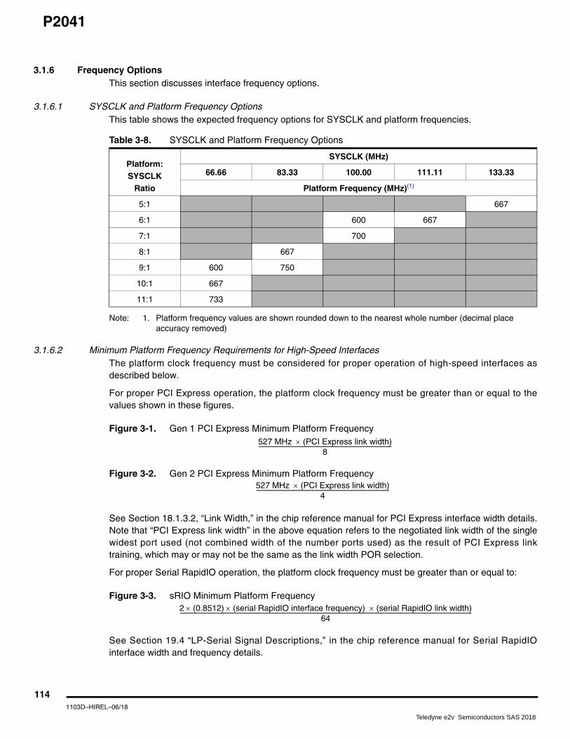
P2041
3.1.6 Frequency Options This section discusses interface frequency options.
3.1.6.1 SYSCLK and Platform Frequency Options This table shows the expected frequency options for SYSCLK and platform frequencies.
Note: 1. Platform frequency values are shown rounded down to the nearest whole number (decimal place accuracy removed)
3.1.6.2 Minimum Platform Frequency Requirements for High-Speed Interfaces The platform clock frequency must be considered for proper operation of high-speed interfaces asdescribed below.
For proper PCI Express operation, the platform clock frequency must be greater than or equal to thevalues shown in these figures.
Figure 3-1. Gen 1 PCI Express Minimum Platform Frequency
Figure 3-2. Gen 2 PCI Express Minimum Platform Frequency
See Section 18.1.3.2, “Link Width,” in the chip reference manual for PCI Express interface width details.Note that “PCI Express link width” in the above equation refers to the negotiated link width of the singlewidest port used (not combined width of the number ports used) as the result of PCI Express linktraining, which may or may not be the same as the link width POR selection.
For proper Serial RapidIO operation, the platform clock frequency must be greater than or equal to:
Figure 3-3. sRIO Minimum Platform Frequency
See Section 19.4 “LP-Serial Signal Descriptions,” in the chip reference manual for Serial RapidIOinterface width and frequency details.
Table 3-8. SYSCLK and Platform Frequency Options
Platform:SYSCLK
Ratio
SYSCLK (MHz)
66.66 83.33 100.00 111.11 133.33
Platform Frequency (MHz)(1)
5:1 667
6:1 600 667
7:1 700
8:1 667
9:1 600 750
10:1 667
11:1 733
527 MHz (PCI Express link width)8
-----------------------------------------------------------------------------------------------
527 MHz (PCI Express link width)4
-----------------------------------------------------------------------------------------------
2 (0.8512) (serial RapidIO interface frequency) (serial RapidIO link width)64
-----------------------------------------------------------------------------------------------------------------------------------------------------------------------------------------------------------------
1141103D–HIREL–06/18
Teledyne e2v Semiconductors SAS 2018

P2041
3.1.7 SerDes PLL Ratio The clock ratio between each of the three SerDes PLLs and their respective externally suppliedSD_REF_CLKn/SD_REF_CLKn inputs is determined by the binary value of the RCW Configuration fieldSRDS_RATIO_Bn as shown in this table. Furthermore, each SerDes lane grouping can be run at aSerDes PLL frequency divider determined by the binary value of the RCW field SRDS_DIV_Bn asshown in Table 3-11.
This table lists the supported SerDes PLL Bank n to SD_REF_CLKn ratios.
These tables list the supported SerDes PLL dividers.
This table shows the PLL divider support for each pair of lanes on SerDes Bank 1.
Note: 1 bit (of 5 total SRDS_DIV_B1 bits) controls each pair of lanes. Because this chip does not have lanes A–B and H–J exposed, the first bit and last bit are not meaningful.
This table shows the PLL dividers supported for each 4-lane for SerDes Banks 2.
Note: 1 bit controls all four lanes of bank 2.
Table 3-9. SerDes PLL Bank n to SD_REF_CLKn Ratios
Binary Value ofSRDS_RATIO_B1
SRDS_PLL_n: SD_REF_CLKn Ratio
n = 1 (Bank) n = 2 (Bank 2)
000 Reserved Reserved
001 Reserved 20:1
010 25:1 25:1
011 40:1 40:1
100 50:1 50:1
101 Reserved 24:1
110 Reserved 30:1
All Others Reserved Reserved
Table 3-10. SerDes Bank 1 PLL Dividers
Binary Value of SRDS_DIV_B1[0:4] SerDes Bank 1 PLL Divider
0b0 Divide by 1 off Bank 1 PLL
0b1 Divide by 2 off Bank 1 PLL
Table 3-11. SerDes Banks 2 PLL Dividers
Binary Value of SRDS_DIV_B2 SerDes Bank 2 PLL Divider
0b0 Divide by 1 off Bank 2 PLL
0b1 Divide by 2 off Bank 2 PLL
1151103D–HIREL–06/18
Teledyne e2v Semiconductors SAS 2018

P2041
3.1.8 Frame Manager (FMan) Clock Select The Frame Managers (FM) can each be synchronous to the platform.
This table describes the clocking options that may be applied to each FM. The clock selection isdetermined by the binary value of the RCW clocking configuration fields FM_CLK_SEL.
Note: 1. For asynchronous mode, max frequency, see Table 3-1.
3.2 Supply Power Default Setting The device is capable of supporting multiple power supply levels on its I/O supplies. The I/O voltageselect inputs, shown in Table 3-13, properly configure the receivers and drivers of the I/Os associatedwith the BVDD, CVDD, and LVDD power planes, respectively.
WARNING
Incorrect voltage select settings can lead to irreversible device damage.
Table 3-12. Frame Manager Clock Select
Binary Value of FM_CLK_SEL FM Frequency
0b0 Platform Clock Frequency /2
0b1 Core Cluster 2 Frequency /2(1)
Table 3-13. I/O Voltage Selection
Signals Value (Binary)
VDD Voltage Selection
BVDD CVDD LVDD
IO_VSEL[0:4]Default (0_0000)
0_0000 3.3 V 3.3 V 3.3 V
0_0001 2.5 V
0_0010 Reserved
0_0011 3.3 V 2.5 V 3.3 V
0_0100 2.5 V
0_0101 Reserved
0_0110 3.3 V 1.8 V 3.3 V
0_0111 2.5 V
0_1000 Reserved
0_1001 2.5 V 3.3 V 3.3 V
0_1010 2.5 V
0_1011 Reserved
0_1100 2.5 V 2.5 V 3.3 V
0_1101 2.5 V
0_1110 Reserved
0_1111 2.5 V 1.8 V 3.3 V
1_0000 2.5 V
1_0001 Reserved
1161103D–HIREL–06/18
Teledyne e2v Semiconductors SAS 2018

P2041
3.3 Power Supply Design This section discusses the power supply design.
3.3.1 PLL Power Supply Filtering Each of the PLLs described in Section 3.1 ”System Clocking” on page 110, is provided with powerthrough independent power supply pins (AVDD_PLAT, AVDD_CCn, AVDD_DDR, and AVDD_SRDSn). AVDD_PLAT,AVDD_CCn and AVDD_DDR voltages must be derived directly from the VDD_CA_CB_PL source through a lowfrequency filter scheme. AVDD_SRDSn voltages must be derived directly from the SVDD source through alow frequency filter scheme.
The recommended solution for PLL filtering is to provide independent filter circuits per PLL powersupply, as illustrated in Figure 3-4, one for each of the AVDD pins. By providing independent filters toeach PLL the opportunity to cause noise injection from one PLL to the other is reduced.
This circuit is intended to filter noise in the PLL’s resonant frequency range from a 500-kHz to 10-MHzrange.
Each circuit must be placed as close as possible to the specific AVDD pin being supplied to minimizenoise coupled from nearby circuits. It must be possible to route directly from the capacitors to the AVDD
pin, which is on the periphery of the footprint, without the inductance of vias.
1_0010 1.8 V 3.3 V 3.3 V
1_0011 2.5 V
1_0100 Reserved
1_0101 1.8 V 2.5 V 3.3 V
1_0110 2.5 V
1_0111 Reserved
1_1000 1.8 V 1.8 V 3.3 V
1_1001 2.5 V
1_1010 Reserved
1_1011 3.3 V 3.3 V 3.3 V
_1_1100
_1_1101
_1_1110
_1_1111
Table 3-13. I/O Voltage Selection (Continued)
Signals Value (Binary)
VDD Voltage Selection
BVDD CVDD LVDD
1171103D–HIREL–06/18
Teledyne e2v Semiconductors SAS 2018
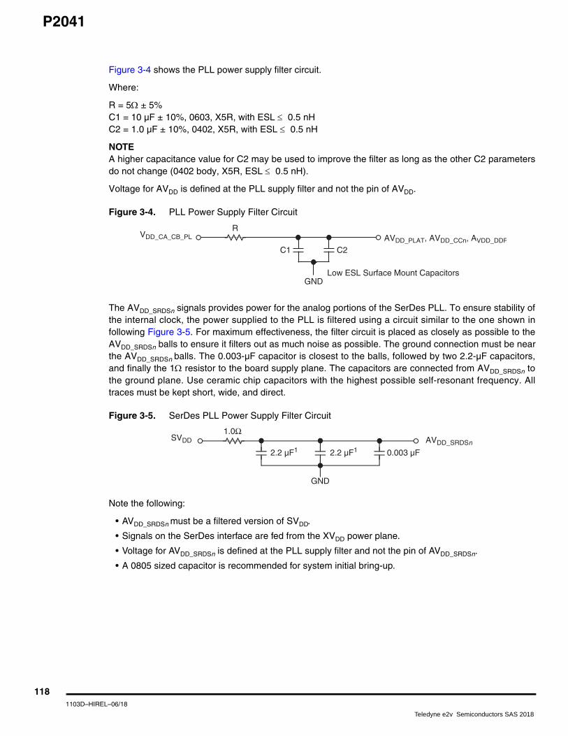
P2041
Figure 3-4 shows the PLL power supply filter circuit.
Where:
R = 5 ± 5%C1 = 10 µF ± 10%, 0603, X5R, with ESL 0.5 nHC2 = 1.0 µF ± 10%, 0402, X5R, with ESL 0.5 nH
NOTEA higher capacitance value for C2 may be used to improve the filter as long as the other C2 parametersdo not change (0402 body, X5R, ESL 0.5 nH).
Voltage for AVDD is defined at the PLL supply filter and not the pin of AVDD.
Figure 3-4. PLL Power Supply Filter Circuit
The AVDD_SRDSn signals provides power for the analog portions of the SerDes PLL. To ensure stability ofthe internal clock, the power supplied to the PLL is filtered using a circuit similar to the one shown infollowing Figure 3-5. For maximum effectiveness, the filter circuit is placed as closely as possible to theAVDD_SRDSn balls to ensure it filters out as much noise as possible. The ground connection must be nearthe AVDD_SRDSn balls. The 0.003-µF capacitor is closest to the balls, followed by two 2.2-µF capacitors,and finally the 1 resistor to the board supply plane. The capacitors are connected from AVDD_SRDSn tothe ground plane. Use ceramic chip capacitors with the highest possible self-resonant frequency. Alltraces must be kept short, wide, and direct.
Figure 3-5. SerDes PLL Power Supply Filter Circuit
Note the following:
• AVDD_SRDSn must be a filtered version of SVDD.
• Signals on the SerDes interface are fed from the XVDD power plane.
• Voltage for AVDD_SRDSn is defined at the PLL supply filter and not the pin of AVDD_SRDSn.
• A 0805 sized capacitor is recommended for system initial bring-up.
VDD_CA_CB_PL
C1 C2
GNDLow ESL Surface Mount Capacitors
RAVDD_PLAT, AVDD_CCn, AVDD_DDR
2.2 µF1 0.003 µF
1.0Ω AVDD_SRDSn
2.2 µF1
GND
SVDD
1181103D–HIREL–06/18
Teledyne e2v Semiconductors SAS 2018

P2041
3.3.2 XVDD Power Supply Filtering XVDD may be supplied by a linear regulator or sourced by a filtered GVDD. Systems may design in bothoptions to allow flexibility to address system noise dependencies.
An example solution for XVDD filtering, where XVDD is sourced from GVDD, is illustrated in Figure 3-6. Thecomponent values in this example filter is system dependent and are still under characterization,component values may need adjustment based on the system or environment noise.
Where:
C1 = 2.2 µF ± 10%, X5R, with ESL 0.5 nHC2 = 2.2 µF ± 10%, X5R, with ESL 0.5 nHF1 = 120 at 100-MHz 2A 25% 0603 FerriteF2 = 120 at 100-MHz 2A 25% 0603 Ferrite
Bulk and decoupling capacitors are added, as needed, per power supply design.
Figure 3-6. XVDD Power Supply Filter Circuit
3.3.3 USB_VDD_1P0 Power Supply Filtering USB_VDD_1P0 must be sourced by a filtered VDD_CA_CB_PL using a star connection. An example solutionfor USB_VDD_1P0 filtering, where USB_VDD_1P0 is sourced from VDD_CA_CB_PL, is illustrated in Figure 3-7. The component values in this example filter is system dependent and are still under characterization;component values may need adjustment based on the system or environment noise.
Where:
C1 = 2.2 µF ± 20%, X5R, with Low ESL (for example, Panasonic ECJ0EB0J225M) F1 = 120 at 100-MHz 2A 25% Ferrite (for example, Murata BLM18PG121SH1)
Bulk and decoupling capacitors are added, as needed, per power supply design.
Figure 3-7. USB_VDD_1P0 Power Supply Filter Circuit
XVDD GVDD
C1 C2
GND
F1
F2
Bulk andDecouplingCapacitors
USB_VDD_1P0 VDD_CA_PL
C1 C1
GND
F1Bulk andDecouplingCapacitors
1191103D–HIREL–06/18
Teledyne e2v Semiconductors SAS 2018

P2041
3.4 Decoupling Recommendations Due to large address and data buses, and high operating frequencies, the device can generate transientpower surges and high frequency noise in its power supply, especially while driving large capacitiveloads. This noise must be prevented from reaching other components in the chip’s system, and the chipitself requires a clean, tightly regulated source of power. Therefore, it is recommended that the systemdesigner place at least one decoupling capacitor at each VDD, BVDD, OVDD, CVDD, GVDD, and LVDD pin ofthe device. These decoupling capacitors should receive their power from separate VDD, BVDD, OVDD,CVDD, GVDD, LVDD, and GND power planes in the PCB, utilizing short traces to minimize inductance.Capacitors may be placed directly under the device using a standard escape pattern. Others maysurround the part.
These capacitors should have a value of 0.01 or 0.1 µF. Only ceramic SMT (surface mount technology)capacitors must be used to minimize lead inductance, preferably 0402 or 0603 sizes.
Additionally, it is recommended that there be several bulk storage capacitors distributed around thePCB, feeding the VDD, BVDD, OVDD, CVDD, GVDD, and LVDD planes, to enable quick recharging of thesmaller chip capacitors. These bulk capacitors should have a low ESR (equivalent series resistance)rating to ensure the quick response time necessary. They should also be connected to the power andground planes through two vias to minimize inductance. Suggested bulk capacitors: 100–330 µF (AVXTPS tantalum or Sanyo OSCON).
3.5 SerDes Block Power Supply Decoupling Recommendations The SerDes block requires a clean, tightly regulated source of power (SVDD and XVDD) to ensure lowjitter on transmit and reliable recovery of data in the receiver. An appropriate decoupling scheme isoutlined below.
Only SMT capacitors must be used to minimize inductance. Connections from all capacitors to powerand ground must be done with multiple vias to further reduce inductance.
• First, the board should have at least 10 × 10-nF SMT ceramic chip capacitors as close as possible to the supply balls of the device. Where the board has blind vias, these capacitors must be placed directly below the chip supply and ground connections. Where the board does not have blind vias, these capacitors must be placed in a ring around the device as close to the supply and ground connections as possible.
• Second, there must be a 1 µF ceramic chip capacitor on each side of the device. This must be done for all SerDes supplies.
• Third, between the device and any SerDes voltage regulator there must be a 10-µF, low ESR SMT tantalum chip capacitor and a 100 µF, low ESR SMT tantalum chip capacitor. This must be done for all SerDes supplies.
1201103D–HIREL–06/18
Teledyne e2v Semiconductors SAS 2018

P2041
3.6 Connection Recommendations To ensure reliable operation, it is highly recommended to connect unused inputs to an appropriate signallevel. All unused active low inputs must be tied to VDD, BVDD, CVDD, OVDD, GVDD, and LVDD as required.All unused active high inputs must be connected to GND. All NC (no-connect) signals must remainunconnected. Power and ground connections must be made to all external VDD, BVDD, CVDD, OVDD,GVDD, LVDD, and GND pins of the device.
The Ethernet controllers 1 and/or 2 input pins may be disabled by setting their respective RCWconfiguration field EC1 (bits 360–361) and EC2 (bits 363–364) to 0b11 = No parallel mode Ethernet.When disabled, these inputs do not need to be externally pulled to an appropriate signal level.
ECn_GTX_CLK125 is a 125-MHz input clock on the dTSEC ports. If the dTSEC ports are not used forRGMII, the ECn_GTX_CLK125 input can be tied off to GND.
If RCW field I2C = 0b0100 or 0b0101 (RCW bits 354–357), the SDHC_WP and SDHC_CD input signalsare enabled for external use. If SDHC_WP and SDHC_CD are selected and not used, they must beexternally pulled low such that SDHC_WP = 0 (write enabled) and SDHC_CD = 0 (card detected).
and SDHC_CD are internally driven such that SDHC_WP = write enabled and SDHC_CD = carddetected and the selected I2C3 or GPIO external pin functionality may be used.
TMP_DETECT pin and LP_TMP DETECT pin are active low input to the Security Monitor (refer to the“Secure Boot and Trust Architecture” chapter of the chip reference manual). If a tamper sensor is used, itmust maintain the signal at the specified voltage until a tamper is detected. A 1K pulldown resistorstrongly recommended. If Trust is used without tamper sensors, tie high. VDD_LP must be connected evenif Low Power features aren’t used. Otherwise, the LP_Section will generate internal errors that willprevent the high power trust section from reaching Trusted/Secure state.
3.6.1 Legacy JTAG Configuration Signals Correct operation of the JTAG interface requires configuration of a group of system control pins asdemonstrated in Figure 3-9. Care must be taken to ensure that these pins are maintained at a validnegated state under normal operating conditions as most have asynchronous behavior and spuriousassertion will give unpredictable results.
Boundary-scan testing is enabled through the JTAG interface signals. The TRST signal is optional in theIEEE Std 1149.1 specification, but it is provided on all processors built on Power Architecturetechnology. The device requires TRST to be asserted during power-on reset flow to ensure that theJTAG boundary logic does not interfere with normal chip operation. While the TAP controller can beforced to the reset state using only the TCK and TMS signals, generally systems assert TRST during thepower-on reset flow. Simply tying TRST to PORESET is not practical because the JTAG interface is alsoused for accessing the common on-chip processor (COP), which implements the debug interface to thechip.
The COP function of these processors allow a remote computer system (typically, a PC with dedicatedhardware and debugging software) to access and control the internal operations of the processor. TheCOP interface connects primarily through the JTAG port of the processor, with some additional statusmonitoring signals. The COP port requires the ability to independently assert PORESET or TRST inorder to fully control the processor. If the target system has independent reset sources, such as voltagemonitors, watchdog timers, power supply failures, or push-button switches, then the COP reset signalsmust be merged into these signals with logic.
If RCW field I2C 0b0100 or 0b0101, thereby selecting either I2C3 or GPIO functionality, SDHC_WP
1211103D–HIREL–06/18
Teledyne e2v Semiconductors SAS 2018

P2041
The arrangement shown in Figure 3-9 allows the COP port to independently assert PORESET or TRST,while ensuring that the target can drive PORESET as well.
The COP interface has a standard header, shown in Figure 3-8, for connection to the target system, andis based on the 0.025" square-post, 0.100" centered header assembly (often called a Berg header). Theconnector typically has pin 14 removed as a connector key.
The COP header adds many benefits such as breakpoints, watch points, register and memoryexamination/modification, and other standard debugger features. An inexpensive option can be to leavethe COP header unpopulated until needed.
There is no standardized way to number the COP header; so emulator vendors have issued manydifferent pin numbering schemes. Some COP headers are numbered top-to-bottom then left-to-right,while others use left-to-right then top-to-bottom. Still others number the pins counter-clockwise from pin1 (as with an IC). Regardless of the numbering scheme, the signal placement recommended in Figure 3-8 is common to all known emulators.
3.6.1.1 Termination of Unused Signals If the JTAG interface and COP header is not used, TELEDYNE e2v recommends the followingconnections:
• TRST must be tied to PORESET through a 0 k isolation resistor so that it is asserted when the system reset signal (PORESET) is asserted, ensuring that the JTAG scan chain is initialized during the power-on reset flow. TELEDYNE e2v recommends that the COP header be designed into the system as shown in Figure 3-9. If this is not possible, the isolation resistor will allow future access to TRST in case a JTAG interface may need to be wired onto the system in future debug situations.
• No pull-up/pull-down is required for TDI, TMS, or TDO.
Figure 3-8. Legacy COP Connector Physical Pinout
3
13
9
5
1
6
10
15
11
7
16
12
8
4
KEYNo pin
1 2COP_TDO
COP_TDI
NC
NC
COP_TRST
COP_VDD_SENSE
COP_CHKSTP_IN
NC
NC
GND
COP_TCK
COP_TMS
COP_SRESET
COP_HRESET
COP_CHKSTP_OUT
1221103D–HIREL–06/18
Teledyne e2v Semiconductors SAS 2018

P2041
Figure 3-9. Legacy JTAG Interface Connection
Notes: 1. The COP port and target board must be able to independently assert PORESET and TRST to the processor in order to fully control the processor as shown here.
2. Populate this with a 10 resistor for short-circuit/current-limiting protection.
3. The KEY location (pin 14) is not physically present on the COP header.
4. Although pin 12 is defined as a No-Connect, some debug tools may use pin 12 as an additional GND pin for improved signal integrity.
5. This switch is included as a precaution for BSDL testing. The switch must be closed to position A during BSDL testing to avoid accidentally asserting the TRST line. If BSDL testing is not being performed, this switch must be closed to position B.
6. Asserting HRESET causes a hard reset on the device.
7. This is an open-drain gate.
PORESET
From TargetBoard Sources
COP_HRESET13
COP_SRESET
HRESET
NC
11
COP_VDD_SENSE 2
6
15
10Ω
10 kΩ10 kΩ
COP_CHKSTP_IN8
COP_TMS
COP_TDO
COP_TDI
COP_TCK
TMS
TDO
TDI
9
1
3
4COP_TRST
7
16
2
10
12
(if any)
CO
P H
ead
er
14 3
10 kΩ
TRST 110 kΩ
10 kΩ
10 kΩ
CKSTP_OUTCOP_CHKSTP_OUT
3
13
9
5
1
6
10
15
11
7
16
12
8
4
KEYNo pin
COP ConnectorPhysical Pinout
1 2
NC
HRESET
NC
OVDD
10 kΩ PORESET1
TCK
4
5 10 kΩ
6
AB
5
System logic
7
1231103D–HIREL–06/18
Teledyne e2v Semiconductors SAS 2018

P2041
3.6.2 Aurora Configuration Signals Correct operation of the Aurora interface requires configuration of a group of system control pins asdemonstrated in Figure 3-10 and Figure 3-11. Care must be taken to ensure that these pins aremaintained at a valid negated state under normal operating conditions as most have asynchronousbehavior and spurious assertion will give unpredictable results.
TELEDYNE e2v recommends that the Aurora 22 pin duplex connector be designed into the system asshown in Figure 3-12 or the 70 pin duplex connector be designed into the system as shown in Figure 3-13.
If the Aurora interface is not used, TELEDYNE e2v recommends the legacy COP header be designedinto the system as described in Section 3.6.1.1 ”Termination of Unused Signals” on page 122.
Figure 3-10. Aurora 22 Pin Connector Duplex Pinout
3
13
9
5
1
6
10
15
11
7
16
12
8
4
1 2TX0+
TX0-
GND
VIO (VSense)
TCK
TMS
TDI
TDO
TRST
Vendor I/O 1
TX1+
TX1-
GND
RX0+
RX0-
17 18
2019
21 22
GND
RX1+
RX1-
Vendor I/O 014
Vendor I/O 3
Vendor I/O 2
RESET
1241103D–HIREL–06/18
Teledyne e2v Semiconductors SAS 2018

P2041
Figure 3-11. Aurora 70 Pin Connector Duplex Pinout
3
13
9
5
1
6
10
15
11
7
16
12
8
4
1 2TX0+
TX0–
GND
VIO (VSense)
TCK
TMS
TDI
TDO
TRST
TX1+
TX1–
GND
RX0+
RX0–
17 18
2019
21 22
GND
RX1+
RX1–
14
RESET
25
35
31
27
23
28
32
37
33
29
38
34
30
26
24GND
TX2+
TX2–
GND
CLK+
CLK-
GND
N/C
GND
TX3+
TX3–
GND
RX2+
39 40
4241
43 44
RX2–
GND
RX3+
GND36
GND
N/C
N/C
47
57
53
49 50
54
59
55
51
60
56
52
48
45 46RX3–
GND
TX4+
N/C
GND
N/C
N/C
GND
N/C
GND
TX4–
GND
TX5+
TX5–
GND
61 62
6463
65 66
TX6+
TX6–
GND
N/C58
N/C
N/C
GND
6867
69 70
TX7+
TX7–
N/C
N/C
Vendor I/O 0
Vendor I/O 1
Vendor I/O 2
Vendor I/O 3
Vendor I/O 4
Vendor I/O 5
1251103D–HIREL–06/18
Teledyne e2v Semiconductors SAS 2018

P2041
Figure 3-12. Aurora 22 Pin Connector Duplex Interface Connection
Notes: 1. The Aurora port and target board must be able to independently assert PORESET and TRST to the processor in order to fully control the processor as shown here.
2. Populate this with a 1 k resistor for short-circuit/current-limiting protection.
3. This switch is included as a precaution for BSDL testing. The switch must be closed to position A during BSDL testing to avoid accidentally asserting the TRST line. If BSDL testing is not being performed, this switch must be closed to position B.
4. Asserting HRESET causes a hard reset on the device. HRESET is not used by the Aurora 22 pin connector.
PORESET
From TargetBoard Sources
RESET22
HRESET
VIO VSense22
1 kΩ
COP_TMS
COP_TDO
COP_TDI
COP_TCK
TMS
TDO
TDI
6
10
8
12TRST
4
1711
(if any)
CO
P H
eade
r
10 kΩ
TRST110 kΩ
10 kΩ
10 kΩ
Duplex 22 ConnectorPhysical Pinout
HRESET
OVDD
10 kΩ PORESET1
TCK
3 10 kΩ
4
AB
3
13
9
5
1
6
10
15
11
7
16
12
8
4
1 2
17 18
2019
21 22
14
20 Vendor I/O 3 N/C
18 Vendor I/O 2 (Aurora Event Out)
16Vendor I/O 1 (Aurora Event In)
14Vendor I/O 0 (Aurora HALT)
5
EVT[4]
EVT[1]
EVT[0]
1TX0_P
3TX0_N
SD_TX09_P
SD_TX09_N
7TX1_P
9TX1_N
SD_TX08_P
SD_TX08_N
13RX0_P
15RX0_N
SD_RX09_P
SD_RX09_N
19RX1_P
21RX1_N
SD_RX08_P
SD_RX08_N
1261103D–HIREL–06/18
Teledyne e2v Semiconductors SAS 2018

P2041
Figure 3-13. Aurora 70 Pin Connector Duplex Interface Connection
Notes: 1. The Aurora port and target board must be able to independently assert PORESET and TRST to the processor in order to fully control the processor as shown here.
2. Populate this with a 1 k resistor for short-circuit/current-limiting protection.
3. This switch is included as a precaution for BSDL testing. The switch must be closed to position A during BSDL testing to avoid accidentally asserting the TRST line. If BSDL testing is not being performed, this switch must be closed to position B.
4. Asserting HRESET causes a hard reset on the device.
5. This is an open-drain gate.
PORESET
From TargetBoard Sources
RESET22
HRESET
VIO VSense22
1 kΩ
COP_TMS
COP_TDO
COP_TDI
COP_TCK
TMS
TDO
TDI
6
10
8
12TRST
4
42,47,48,53,54,29,30,35,36,41,
(if any)
CO
P H
eade
r
TRST110 kΩ
10 kΩ
10 kΩ
Duplex 70
HRESET
OVDD
10 kΩ PORESET1
TCK
3 10 kΩ
4
AB
20 Vendor I/O 3 N/C
18 Vendor I/O 2 (Aurora Event Out)
16Vendor I/O 1 (Aurora Event In)
14Vendor I/O 0 (Aurora HALT)
5,11,17,23,24,
EVT[4]
EVT[1]
EVT[0]
1TX0_P
3TX0_N
SD_TX09_P
SD_TX09_N
7TX1_P
9TX1_N
SD_TX08_P
SD_TX08_N
13RX0_P
15RX0_N
SD_RX09_P
SD_RX09_N
19RX1_P
21RX1_N
SD_RX08_P
SD_RX08_N
3
13
9
5
1
6
10
15
11
7
16
12
8
4
1 2
17 18
2019
21 22
14
25
35
31
27
23
28
32
37
33
29
38
34
30
26
24
39 40
4241
43 44
36
47
57
53
49 50
54
59
55
51
60
56
52
48
45 46
61 62
6463
65 66
58
6867
69 70
34Vendor I/O 5 (Aurora HRESET)
32 Vendor I/O 4 N/C EVT[4]
31,33,37,38,
N/C39,40,43,44,45,46,49,50,51,52,55,56,57,58,61,62,63,64,67,68,
25,26,27,28,
69,70
59,60,65,66
ConnectorPhysical Pinout
10 kΩ
10 kΩ
5
1271103D–HIREL–06/18
Teledyne e2v Semiconductors SAS 2018

P2041
3.6.3 Guidelines for High-Speed Interface Termination This section provides the guidelines for when the SerDes interface is either entirely unused or partlyunused.
3.6.3.1 SerDes Interface Entirely Unused If the high-speed SerDes interface is not used at all, the unused pin must be terminated as described inthis section. The following pins must be left unconnected:
• SD_TX[7:2], SD_TX[13:10]
• SD_TX[7:2], SD_TX[13:10]
• SD_IMP_CAL_RX
• SD_IMP_CAL_TX
The following pins must be connected to SGND:
• SD_RX[7:2], SD_RX[13:10]
• SD_RX[13:10], SD_RX[13:10]
• SD_REF_CLK1, SD_REF_CLK2
• SD_REF_CLK1, SD_REF_CLK2
In the RCW configuration fields SRDS_LPD_B1 and SRDS_LPD_B2, all bits must be set to power downall the lanes in each bank. RCW configuration field SRDS_EN may be cleared to power down theSerDes block for power saving. Setting
RCW[SRDS_EN] = 0 power-downs the PLLs of both banks.
Additionally, software may configure SRDSBnRSTCTL[SDRD] = 1 for the unused banks to power downthe SerDes bank PLLs to save power.
Note that both SVDD and XVDD must remain powered.
3.6.3.2 SerDes Interface Partly Unused If only part of the high speed SerDes interface pins are used, the remaining high-speed serial I/O pinsmust be terminated as described in this section.
The following unused pins must be left unconnected:
• SD_TX[n]
• SD_TX[n]
The following unused pins must be connected to SGND:
• SD_RX[n]
• SD_RX[n]
• SD_REF_CLK1, SD_REF_CLK1 (If entire SerDes bank 1 unused)
• SD_REF_CLK2, SD_REF_CLK2 (If entire SerDes bank 2 unused)
In the RCW configuration field for each bank SRDS_LPD_Bn with unused lanes, the respective bit foreach unused lane must be set to power down the lane.
1281103D–HIREL–06/18
Teledyne e2v Semiconductors SAS 2018
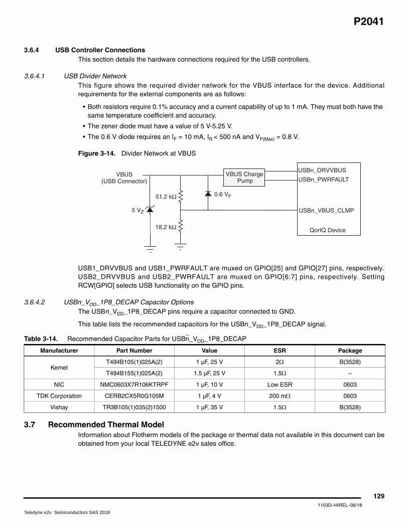
P2041
3.6.4 USB Controller Connections This section details the hardware connections required for the USB controllers.
3.6.4.1 USB Divider Network This figure shows the required divider network for the VBUS interface for the device. Additionalrequirements for the external components are as follows:
• Both resistors require 0.1% accuracy and a current capability of up to 1 mA. They must both have the same temperature coefficient and accuracy.
• The zener diode must have a value of 5 V-5.25 V.
• The 0.6 V diode requires an IF = 10 mA, IR < 500 nA and VF(Max) = 0.8 V.
Figure 3-14. Divider Network at VBUS
USB1_DRVVBUS and USB1_PWRFAULT are muxed on GPIO[25] and GPIO[27] pins, respectively.USB2_DRVVBUS and USB2_PWRFAULT are muxed on GPIO[6:7] pins, respectively. SettingRCW[GPIO] selects USB functionality on the GPIO pins.
3.6.4.2 USBn_VDD_1P8_DECAP Capacitor Options The USBn_VDD_1P8_DECAP pins require a capacitor connected to GND.
This table lists the recommended capacitors for the USBn_VDD_1P8_DECAP signal.
3.7 Recommended Thermal Model Information about Flotherm models of the package or thermal data not available in this document can beobtained from your local TELEDYNE e2v sales office.
USBn_DRVVBUS
18.2 kΩ
USBn_VBUS_CLMP
51.2 kΩ
QorIQ Device
5 VZ
0.6 VF
USBn_PWRFAULTVBUS Charge
PumpVBUS
(USB Connector)
Table 3-14. Recommended Capacitor Parts for USBn_VDD_1P8_DECAP
Manufacturer Part Number Value ESR Package
Kemet T494B105(1)025A(2) 1 µF, 25 V 2 B(3528)
T494B155(1)025A(2) 1.5 µF, 25 V 1.5 –
NIC NMC0603X7R106KTRPF 1 µF, 10 V Low ESR 0603
TDK Corporation CERB2CX5R0G105M 1 µF, 4 V 200 m 0603
Vishay TR3B105(1)035(2)1500 1 µF, 35 V 1.5 B(3528)
1291103D–HIREL–06/18
Teledyne e2v Semiconductors SAS 2018
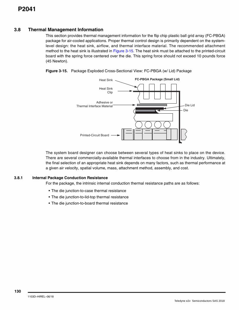
P2041
3.8 Thermal Management Information This section provides thermal management information for the flip chip plastic ball grid array (FC-PBGA)package for air-cooled applications. Proper thermal control design is primarily dependent on the system-level design: the heat sink, airflow, and thermal interface material. The recommended attachmentmethod to the heat sink is illustrated in Figure 3-15. The heat sink must be attached to the printed-circuitboard with the spring force centered over the die. This spring force should not exceed 10 pounds force(45 Newton).
Figure 3-15. Package Exploded Cross-Sectional View: FC-PBGA (w/ Lid) Package
The system board designer can choose between several types of heat sinks to place on the device.There are several commercially-available thermal interfaces to choose from in the industry. Ultimately,the final selection of an appropriate heat sink depends on many factors, such as thermal performance ata given air velocity, spatial volume, mass, attachment method, assembly, and cost.
3.8.1 Internal Package Conduction Resistance For the package, the intrinsic internal conduction thermal resistance paths are as follows:
• The die junction-to-case thermal resistance
• The die junction-to-lid-top thermal resistance
• The die junction-to-board thermal resistance
Adhesive orThermal Interface Material
Heat Sink FC-PBGA Package (Small Lid)
Heat SinkClip
Printed-Circuit Board
Die
Die Lid
1301103D–HIREL–06/18
Teledyne e2v Semiconductors SAS 2018
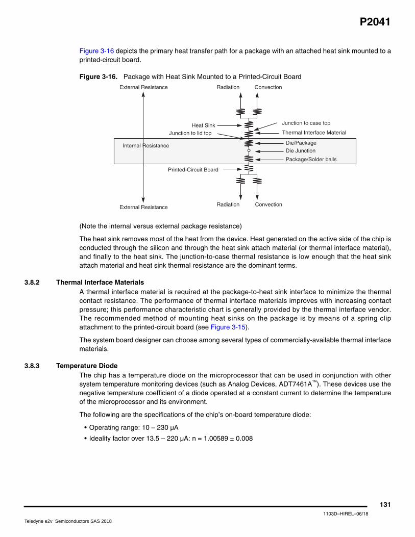
P2041
Figure 3-16 depicts the primary heat transfer path for a package with an attached heat sink mounted to aprinted-circuit board.
Figure 3-16. Package with Heat Sink Mounted to a Printed-Circuit Board
(Note the internal versus external package resistance)
The heat sink removes most of the heat from the device. Heat generated on the active side of the chip isconducted through the silicon and through the heat sink attach material (or thermal interface material),and finally to the heat sink. The junction-to-case thermal resistance is low enough that the heat sinkattach material and heat sink thermal resistance are the dominant terms.
3.8.2 Thermal Interface Materials A thermal interface material is required at the package-to-heat sink interface to minimize the thermalcontact resistance. The performance of thermal interface materials improves with increasing contactpressure; this performance characteristic chart is generally provided by the thermal interface vendor.The recommended method of mounting heat sinks on the package is by means of a spring clipattachment to the printed-circuit board (see Figure 3-15).
The system board designer can choose among several types of commercially-available thermal interfacematerials.
3.8.3 Temperature Diode The chip has a temperature diode on the microprocessor that can be used in conjunction with othersystem temperature monitoring devices (such as Analog Devices, ADT7461A™). These devices use thenegative temperature coefficient of a diode operated at a constant current to determine the temperatureof the microprocessor and its environment.
The following are the specifications of the chip’s on-board temperature diode:
• Operating range: 10 – 230 µA
• Ideality factor over 13.5 – 220 µA: n = 1.00589 ± 0.008
External Resistance
External Resistance
Internal Resistance
Radiation Convection
Radiation
Heat Sink
Printed-Circuit Board
Die JunctionDie/Package
Junction to lid top
Junction to case top
Thermal Interface Material
Package/Solder balls
Convection
1311103D–HIREL–06/18
Teledyne e2v Semiconductors SAS 2018

P2041
4. Package Information The following section describes the detailed content and mechanical description of the package.
4.1 Package Parameters for the FC-PBGA The package parameters are as provided in the following list. The package type is 23 mm × 23 mm,780 flip chip plastic ball grid array (FC-PBGA).
Package outline 23 mm × 23 mm
Interconnects 780
Ball Pitch 0.8 mm
Ball Diameter (typical) 0.40 mm
Solder Balls 96.5% Sn, 3% Ag, 0.5% Cu
Module height (typical) 2.21 mm to 2.51 mm (Maximum)
1321103D–HIREL–06/18
Teledyne e2v Semiconductors SAS 2018
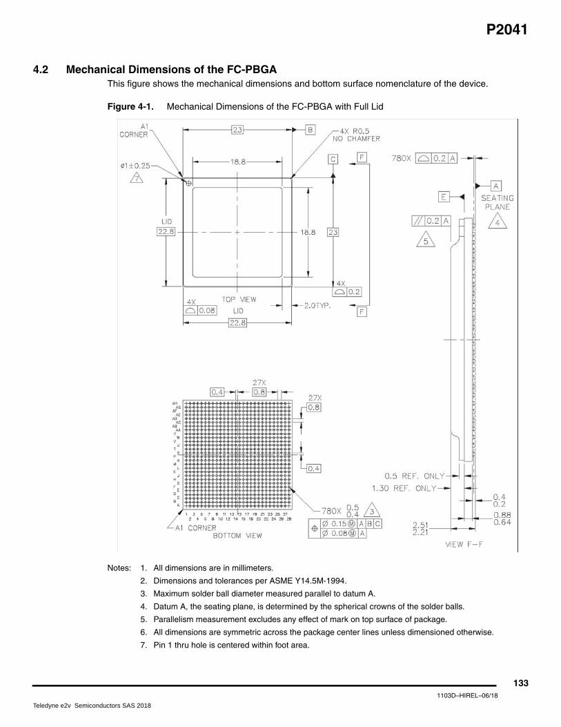
P2041
4.2 Mechanical Dimensions of the FC-PBGA This figure shows the mechanical dimensions and bottom surface nomenclature of the device.
Figure 4-1. Mechanical Dimensions of the FC-PBGA with Full Lid
Notes: 1. All dimensions are in millimeters.
2. Dimensions and tolerances per ASME Y14.5M-1994.
3. Maximum solder ball diameter measured parallel to datum A.
4. Datum A, the seating plane, is determined by the spherical crowns of the solder balls.
5. Parallelism measurement excludes any effect of mark on top surface of package.
6. All dimensions are symmetric across the package center lines unless dimensioned otherwise.
7. Pin 1 thru hole is centered within foot area.
1331103D–HIREL–06/18
Teledyne e2v Semiconductors SAS 2018

P2041
5. Security Fuse Processor The device implements the QorIQ platform’s Trust Architecture supporting capabilities such as secureboot. Use of the Trust Architecture features is dependent on programming fuses in the Security FuseProcessor (SFP). The details of the Trust Architecture and SFP can be found in the chip referencemanual.
In order to program SFP fuses, the user is required to supply 1.5 V to the POVDD pin per Section 2.2”Power Up Sequencing” on page 38. POVDD should only be powered for the duration of the fuseprogramming cycle, with a per device limit of two fuse programming cycles. All other times POVDD mustbe connected to GND. The sequencing requirements for raising and lowering POVDD are shown inFigure 2-2. To ensure device reliability, fuse programming must be performed within the recommendedfuse programming temperature range per Table 2-2.
Users not implementing the QorIQ platform’s Trust Architecture features are not required to programfuses and should connect POVDD to GND.
6. Ordering InformationContact your local TELEDYNE e2v sales office or regional marketing team for ordering information.
This table provides the TELEDYNE e2v QorIQ platform part numbering nomenclature. Not all possiblecombinations of part numbers implied by the part numbering scheme are supported. For a list ofavailable part numbers, contact your TELEDYNE e2v Sales office. Each part number also contains arevision code which refers to the die mask revision number.
Notes: 1. For availability of the different versions, contact your local TELEDYNE e2v sales office.
2. The letter X in the part number designates a "Prototype" product that has not been qualified by TELEDYNE e2v. Reliability of a PCX part-number is not guaranteed and such part-number shall not be used in Flight Hardware. Product changes may still occur while shipping prototypes.
3. Processor core frequencies supported by parts addressed by this specification only. Not all parts described in this specification support all core frequencies. Additionally, parts addressed by part number specifications may support other maximum core frequencies.
7. Definitions
7.1 Life Support ApplicationsThese products are not designed for use in life support appliances, devices or systems wheremalfunction of these products can reasonably be expected to result in personal injury. TELEDYNE e2vcustomers using or selling these products for use in such applications do so at their own risk and agreeto fully indemnify TELEDYNE e2v for any damages resulting from such improper use or sale.
Table 6-1. Ordering Information
p n nn n t e n c d r
Generation Platform Number of Cores Derivative Temperature
Range Encryption Package Type CPU Freq DDR Data Rate Die Revision
P(X) = 45 nm 2 04 1F = –40/+125
M = –55/+125
E = SEC present
N = SEC not present
3 = FC-PBGAC4: Lead freeC5: Leaded
7 = FC-PBGAC4/C5: Lead free
M = 1200 MHzN = 1333 MHzP = 1500 MHz
M = 1200 MT/sN= 1333 MT/s
B = Rev 1.1
C = Rev 2
1341103D–HIREL–06/18
Teledyne e2v Semiconductors SAS 2018

P2041
8. Revision HistoryThis table provides revision history for this document.
Table 8-1. Revision History
Rev. No Date Substantive Change(s)
1103D 09/2017 Updated Table 2-5, “Device Power Dissipation,” on page 41
1103C 05/2014 Updated Table 2-5, “Device Power Dissipation,” on page 41
1103B 09/2013Updated Table 6-1, “Ordering Information,” on page 134 with added C = Rev 2 and changed Package Type.
1103A 11/2012 Initial revision
1351103D–HIREL–06/18
Teledyne e2v Semiconductors SAS 2018

P2041
1361103D–HIREL–06/18
Teledyne e2v Semiconductors SAS 2018

P2041
Table of Contents
MAIN FEATURES ...................................................................................... 1
1 Pin Assignments and Reset States ........................................................ 2
1.1780 FC-PBGA Ball Layout Diagrams ........................................................................2
1.2Pinout List ..................................................................................................................8
2 Electrical Characteristics ...................................................................... 33
2.1Overall DC Electrical Characteristics ......................................................................33
2.2Power Up Sequencing .............................................................................................38
2.3Power Down Requirements .....................................................................................40
2.4Power Characteristics .............................................................................................41
2.5Thermal ...................................................................................................................44
2.6Input Clocks .............................................................................................................44
2.7RESET Initialization .................................................................................................47
2.8Power-on Ramp Rate ..............................................................................................47
2.9DDR3 and DDR3L SDRAM Controller ....................................................................48
2.10eSPI .......................................................................................................................55
2.11DUART ..................................................................................................................57
2.12Ethernet: Data path Three-Speed Ethernet (dTSEC), Management Interface,IEEE Std 1588 58
2.13USB .......................................................................................................................66
2.14Enhanced Local Bus Interface ..............................................................................67
2.15Enhanced Secure Digital Host Controller (eSDHC) ..............................................71
2.16Multicore Programmable Interrupt Controller (MPIC) Specifications .....................73
2.17JTAG Controller .....................................................................................................74
2.18I2C .........................................................................................................................76
2.19GPIO .....................................................................................................................78
2.20High-Speed Serial Interfaces (HSSI) .....................................................................79
3 Hardware Design Considerations ...................................................... 110
3.1System Clocking ....................................................................................................110
3.2Supply Power Default Setting ................................................................................116
3.3Power Supply Design ............................................................................................117
3.4Decoupling Recommendations .............................................................................120
3.5SerDes Block Power Supply Decoupling Recommendations ...............................120
3.6Connection Recommendations .............................................................................121
i1103D–HIREL–06/18
Teledyne e2v Semiconductors SAS 2018
P2041
3.7Recommended Thermal Model .............................................................................129
3.8Thermal Management Information ........................................................................130
4 Package Information ........................................................................... 132
4.1Package Parameters for the FC-PBGA .................................................................132
4.2Mechanical Dimensions of the FC-PBGA .............................................................133
5 Security Fuse Processor ..................................................................... 134
6 Ordering Information ........................................................................... 134
7 Definitions ............................................................................................ 134
7.1Life Support Applications .......................................................................................134
8 Revision History .................................................................................. 135
ii1103D–HIREL–06/18
Teledyne e2v Semiconductors SAS 2018