apd and spad receivers - tu wien
TRANSCRIPT
XXX-X-XXXX-XXXX-X/XX/$XX.00 ©20XX IEEE
APD and SPAD ReceiversInvited Paper
Horst ZimmermannTU Wien, Institute of Electrodynamics, Microwave and Circuit Engineering
Gusshausstr. 25/3541040 Vienna, Austria
—Integrated receivers with avalanche photodiodes (APDs) and single-photon avalanche diodes (SPADs) fabricated in 0.35µm CMOS and BiCMOS technologies are introduced. The APD receivers were used in error-free optical wireless communication (OWC) experiments with maximum trans-mission distances from 11m to 27m at 1Gb/s and from 6.5m to 16.5m at 2Gb/s without receiver lense and without optical filter. The APD receivers work up to and exceeding 2000lx ambient light. The newest trend are SPAD-based receivers, which reduce the gap to the quantum limit. The state of the art of SPAD receivers will be summarized and reviewed also in comparison to APD receivers.
I. INTRODUCTION
Visible Light Communication (VLC) and Light Fidelity (LiFi) are very interesting for wireless communication in indoor networks due to immunity against electromagnetic interference and high bandwidth [1]. Despite the limited modulation bandwidth of LEDs used for room lighting, they are the first choice in VLC systems because of their large optical power and efficiency [2].
The measured spectra of a white LED, of two OSRAM halogen lamps and a fluorescent office lighting are shown in Fig. 1 [3]. A wavelength of about 680nm for indoor OWC is a good choice for fluorescent lighting, LED and halogen 64627. For the broadcasting (down-stream) in VLC the blue spectral part of white LEDs for room lighting is used. A wavelength of 450nm for the up-stream in OWC, however, is not a good choice in presence of white LED room lighting.
Fig. 1. Spectra of indoor light sources
Mainly the up-stream direction will be addressed here. Since optical communication requires very good sensitivies, avalanche photodiodes (APDs) or single-photon avalanche diodes (SPADs) will be needed. Due to the low-cost potential of OEICs, receivers with integrated APDs or SPADs will be essential for the progress of wireless optical communication.
II. APDS AND SPADS
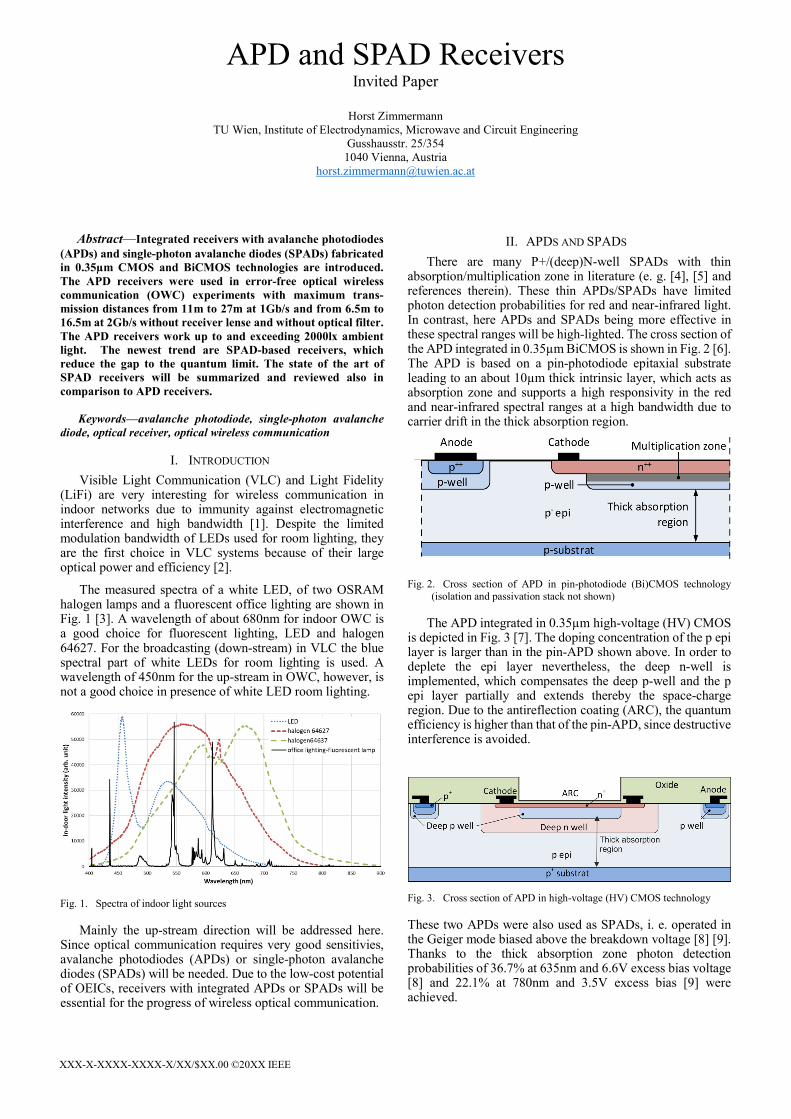
There are many P+/(deep)N-well SPADs with thin absorption/multiplication zone in literature (e. g. [4], [5] and references therein). These thin APDs/SPADs have limited photon detection probabilities for red and near-infrared light. In contrast, here APDs and SPADs being more effective in these spectral ranges will be high-lighted. The cross section of the APD integrated in 0.35µm BiCMOS is shown in Fig. 2 [6].The APD is based on a pin-photodiode epitaxial substrate leading to an about 10µm thick intrinsic layer, which acts as absorption zone and supports a high responsivity in the red and near-infrared spectral ranges at a high bandwidth due to carrier drift in the thick absorption region.
Fig. 2. Cross section of APD in pin-photodiode (Bi)CMOS technology(isolation and passivation stack not shown)
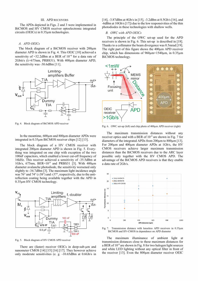
The APD integrated in 0.35µm high-voltage (HV) CMOSis depicted in Fig. 3 [7]. The doping concentration of the p epi layer is larger than in the pin-APD shown above. In order to deplete the epi layer nevertheless, the deep n-well is implemented, which compensates the deep p-well and the p epi layer partially and extends thereby the space-charge region. Due to the antireflection coating (ARC), the quantum efficiency is higher than that of the pin-APD, since destructive interference is avoided.
Fig. 3. Cross section of APD in high-voltage (HV) CMOS technology
These two APDs were also used as SPADs, i. e. operated in the Geiger mode biased above the breakdown voltage [8] [9]. Thanks to the thick absorption zone photon detection probabilities of 36.7% at 635nm and 6.6V excess bias voltage [8] and 22.1% at 780nm and 3.5V excess bias [9] were achieved.
III. APD RECEIVERS
The APDs depicted in Figs. 2 and 3 were implemented in BiCMOS and HV CMOS receiver optoelectronic integrated circuits (OEICs) in 0.35µm technologies.
A. APD OEICsThe block diagram of a BiCMOS receiver with 200µm
diameter APD is shown in Fig. 4. This OEIC [10] achieved a sensitivity of 32.2dBm at a BER of 10 9 for a data rate of 2Gbit/s ( =675nm, PRBS31). With 400µm diameter APD, the sensitivity was -30.6dBm [11].
Fig. 4. Block diagram of BiCMOS APD receiver
In the meantime, 600µm and 800µm diameter APDs were integrated in 0.35µm BiCMOS receiver chips [12] [13].
The block diagram of a HV CMOS receiver with integrated 200µm diameter APD is shown in Fig. 5. Every-thing was integrated on one chip with exception of the two 100nF capacitors, which enabled a lower cut-off frequency of 16kHz. This receiver achieved a sensitivity of -35.5dBm at 1Gb/s, 675nm, BER=10-9 and PRBS31 [3]. With 400µm diameter avalanche photodiode, the sensitivity worsened only slightly to -34.7dBm [3]. The maximum light incidence angle was 76° and 74° (±38°) and ±37°, respectively, due to the anti-reflection coating being available together with the APD in 0.35µm HV CMOS technology.
Fig. 5. Block diagram of HV CMOS APD receiver
There are (faster) receiver OEICs in deep-sub-µm and nanometer CMOS [14] [15] [16] [17]. They however achieve only moderate sensitivities (e. g. -10.65dBm at 0.6Gb/s in
[14], -3.87dBm at 4Gb/s in [15], -3.2dBm at 8.5Gb/s [16], and -6dBm at 10Gb/s [17]) due to the low responsivities of the thin photodiodes in these technologies with shallow wells.
B. OWC with APD OEICsThe principle of the OWC set-up used for the APD
receivers is shown in Fig. 6. This set-up is described in [18].Thanks to a collimator the beam divergence was 0.5mrad [19]. The right part of this figure shows the 400µm APD receiver chip, which has dimensions of 960µm×1540µm, in 0.35µm BiCMOS technology.
Fig. 6. OWC set-up (left) and chip photo of 400µm APD receiver (right)
The maximum transmission distances without any receiver optics and with a BER of 10-9 are shown in Fig. 7 for diameters of the integrated APDs from 200µm to 800µm [13]. For 200µm and 400µm diameter APDs at 1Gb/s, the HV CMOS receivers achieve larger maximum transmission distances than the BiCMOS receivers due to the ARC layer possible only together with the HV CMOS APD. The advantage of the BiCMOS APD receivers is that they enable a data rate of 2Gb/s.
Fig. 7. Transmission distance with lenseless APD receivers in 0.35µm BiCMOS and HV-CMOS in dependence on APD diameter
The maximum illuminance of ambient light attransmission distances close to these maximum distances for a BER of 10-9 are shown in Fig. 8 for two halogen light sources and white LED lighting without any optical filter in front of the receiver [13]. Even the 800µm diameter receiver OEIC

works error-free up to about 1klx for halogen lamp 64637 and up to 1.6klx with white LED lighting.
Fig. 8. Maximum illuminance of ambient light in dependence on APD diameter
IV. SPAD RECEIVERS
The excess noise of APDs limits the sensitivity of receivers using APDs in the linear mode. The improvement of the sensitivity of APD receivers compared to PIN photodiode receivers, therefore, is smaller than the avalanche multiplication factor being present in these APDs. The idea to exploit the much higher gain of SPADs (APDs in the Geiger mode) in optical receivers therefore came up [20].
A. SPAD OEICsSPADs unfortunately are subject to dark counts, i. e. they
can fire without a photon being absorbed due to thermal carrier generation or band-to-band tunneling. In addition afterpulses can occur, when charge carriers are released from traps statistically. In addition optical cross talk occurs, because during impact ionization in large avalanches photons are emitted, which can be absorbed in adjacent SPADs and trigger an avalanche there. Because of these parasitic events an optical receiver containing only one SPAD cannot reach the BER limit of error correction of 2.10-3 [21]. At least several SPADs and a detection threshold of several avalanche events, i. e. several photons, for a logical “1” are necessary to reduce the BER far enough. The consequence is actually that the quantum limit never can be reached.
The chip photo of a SPAD receiver OEIC with an array of 4 SPADs is shown in Fig. 9. This 4-SPAD receiver in 0.35µm CMOS was introduced in [8].
Fig. 9. Chip photo of 4-SPAD receiver
The BER results of this SPAD receiver characterized in a dark box with light signals coupled into the SPAD array with an optical fiber are shown in Fig. 10 [8].
Fig. 10. BER of the 4-SPAD receiver on the average optical input power
Another 4-SPAD receiver with a dead time of 3.5ns and implemented digital processing of the four SPAD signals was characterized up to 200Mb/s [22].
An optical receiver in 0.13µm CMOS imaging technology with a 64×64 SPAD array allowing dead times longer than a bit duration was introduced in [23]. With OOK a data rate of 400Mb/s at a sensitivity of -49.9dBm with 450nm light was reported. For 4-PAM at 500Mb/s an optical power of -46.1dBm was necessary. The electrical power consumption was 230pJ/bit [23].
B. OWC with SPAD ReceiversThe set-up for OWC with SPAD receivers is shown in Fig.
11. A dark box having a small optical window with an interference filter (centered at 635nm or 650nm, both with
=10nm, FWHM) was used [24] [25].
Fig. 11. OWC set-up for SPAD receivers with mirror to double the distance

The 4-SPAD receiver shown in Fig. 9 was used in OWC experiments. First, a 635nm light source using a modulator was used and an optical output power of less than 1µW was sufficient to achieve a BER smaller than 2.10-3 at 50Mb/s over a distance of 2m [24]. For the next experiments a 650nm RC-LED from Firecomms with 1.1mW output power and a collimator leading to a beam divergence of less than 0.038rad were used [25]. The resulting BERs for NRZ and distances up to 6m are depicted in Fig. 12. The maximum distance for a BER below the FEC limit was 5.3m. For a distance of 5.0m, the BER was 1.9.10-3 at 2klx ambient light illuminance [25].
The influence of the duty cycle on the BER was investigated in [26]. Figure 13 shows the obtained BERs at a distance of 3m. The data rate could be increased to 75Mb/s. Lowest BER were achieved at duty cycles around 50%. RZ was also found to be better than NRZ in [8].
Over a very short distance, a data rate of 200Mb/s with a receiver containing 60 SPADs was achieved [27]. Over a distance of 2m a data rate of 60Mb/s with three 128×32 SPAD array receivers for 20Mb/s each was reported [28].
Fig. 12. BER in dependence on OWC distance with SPAD receiver
Fig. 13. BER in dependence on duty ratio for OWC with SPAD receiver
V. COMPARISON
Figure 14 summarizes and compares the sensitivities achieved with APD and SPAD receivers as well as the distances to the quantum limit. The quantum limit depends on the light wavelength used. The APD receivers achieved BERs below 10-9, whereas the SPAD receivers reached only BERs below 2.10-3.
Fig. 14. Sensitivities of APD and SPAD receivers with distances to the quantum limit (EF: [20], BG: [29], HZ: [8], BS: [22], MC: [30], O’B: [31], TJ: [10] [11], DM:[3])
The 32×32 SPAD receiver published in 2013 [20] showed at 100Mb/s a distance to the quantum limit of 31.7dB partly due to its large dynamic range and the BER of 10-9. A SPAD receiver with an integrated gating circuit achieved distances to the quantum limit of 12.7dB at 20Mb/s and 15.7dB at 50Mb/s [29]. The sensitivity of the 4-SPAD receiver shown in Fig. 9 was 18.7dB above the quantum limit. Another 4-SPAD receiver with a short dead time of 3.5ns reached a data rate of 100Mb/s and a distance to the quantum limit of about 21dB[22]. Just recently a 64×64 SPAD receiver achieved a gap to the quantum limit of 12.2dB at 400Mb/s.
For a linear-mode APD receiver having a large sensitive area a sensitivity of -38.5dBm was reported at 155Mb/s [30]. A receiver with a 1.95mm diameter discrete APD had a sensitivity of -38dBm at 280Mb/s [31] corresponding to a distance to the quantum limit of 23.8dB. The BiCMOS receiver with the integrated 400µm diameter APD described above achieved a gap to the quantum limit of 24.4dB at 500Mb/s [11]. The HV CMOS APD receiver described in [3]reached a gap to the quantum limit of 19.6dB at 1Gb/s and the BiCMOS APD receiver introduced in [10] is characterized by a distance to the quantum limit of 19.9dB at 2Gb/s. The energy per bit of the APD BiCMOS receiver of [10] is 122pJ/bit at 2Gb/s, where its sensitivity is -32.2dBm, whereby a 50driver was included, which was only necessary for characterization with oscilloscope and bit error analyzer. The HV CMOS APD receiver of [3] dissipates 182pJ/bit at 1Gb/s also including 50 driver. The 64×64 SPAD receiver of [23]needs 230pJ/bit.
VI. CONCLUSIONS
Integrated APD HV-CMOS and BiCMOS receivers in 0.35µm technology achieve quite good sensitivities even at APD diameters of 200µm and more thanks to the small ratio of the ionization coefficients of these integrated APDs of down to 0.1 [32]. Gaps to the quantum limit of less than 20dB were achieved with APD receivers even at data rates of 1Gb/s and 2Gb/s with BER=10-9. In-door optical wireless communi-cation with lenseless APD receivers is possible up to transmission distances of 27m at 1Gb/s and up to 16.5m at 2Gb/s and ambient light illuminances of up to 950lx with halogen lighting and 1600lx with LED lighting. At shorter transmission distances higher ambient light illuminances of up to 6klx are possible using APD receivers without any optical filter.
SPAD receivers are not so mature yet, although first receivers with gaps to the quantum limit down to 12.7dB and

12.2dB were introduced. The electrical power consumption per bit of SPAD receivers is larger than that of APD receivers even when neglecting the power for error correction of SPAD receivers. The SPAD receivers, however, suffer from the parasitic dark counts, afterpulsing and crosstalk, all worsening the BER and making error correction indispensable, which needs additional complexity and electrical power. These parasitics of SPADs actually represent a barrier for further improving the sensitivity and limit the data rate, which is much smaller than that achievable with linear-mode APD receivers. OWC with SPADs is more difficult than with APDs, because counts from background light photons worsen the sensitivity and require to limit the receiver field of view.
ACKNOWLEDGMENT
The author thanks his coworkers at TU Wien, especially M. Hofbauer, K. Schneider-Hornstein, B. Goll, H. Mahmoudi,D. Milovancev, and B. Steindl for excellent work. Funding from the Austrian Science Foundation (FWF) in the project P28335-N30 is acknowledged.
REFERENCES
[1] D. Karunatilaka, F. Zafar, V. Kalavally, R. Parthiban, “LED based indoor visible light communications: state of the art”, IEEE Communications Surveys & Tutorials, vol. 17, no. 3, pp. 1649-1678, 2015.
[2] T. Komine, M. Nakagawa, “Fundamental analysis for visible-light communication system using LED lights”, IEEE Trans. Consumer Electronics, vol. 50, no. 1, pp. 100-107, 2004.
[3] D. Milovancev, P. Brandl, T. Jukic, B. Steindl, N. Vokic, and H. Zimmermann, “Optical wireless APD receivers in 0.35µm HV CMOS technology with large detection area“, Opt. Express, vol. 27, no. 9, pp. 11930-11945, 2019.
[4] D. Bronzi, S. Tisa, F. Villa, S. Bellisai, A. Tosi, F. Zappa, “Fast Sensing and Quenching of CMOS SPADs for Minimal Afterpulsing Effects”, IEEE Photonics Technology Letters, vol. 25, no. 8, pp. 776-779, 2013.
[5] M.-J. Lee, A. R. Ximenes, P. Padmanabhan, T.-J. Wang, K.-C. Huang, Y. Yamashita, D.-N. Yaung, E. Charbon, “High-performance back-illuminated three-dimensional stacked single-photon avalanche diode implemented in 45-nm CMOS technology”, IEEE J. Selected Topics in Quantum Electronics, vol. 24, no. 6, art. 3801809, Nov./Dec. 2018.
[6] B. Steindl, W. Gaberl, R. Enne, S. Schidl, K. Schneider-Hornstein, H. Zimmermann, ‘Linear Mode Avalanche Photodiode with 1 GHz Bandwidth in 0.35µm CMOS’, IEEE Photonics Technology Letters, vol. 26, no. 26, pp. 1511-1514 (2014).
[7] B. Steindl, R. Enne, S. Schidl, H. Zimmermann, ‘Linear Mode APD with High Responsivity Integrated in High-Voltage CMOS’, IEEE Electron Device Letters, vol. 35, no. 9, pp. 897-899, 2014.
[8] H. Zimmermann, B. Steindl, M. Hofbauer, and R. Enne, “Integrated fiber optical receiver reducing the gap to the quantum limit,” Sci. Rep., vol. 7, Jun. 2017, Art. no. 2652.
[9] B. Steindl, R. Enne, H. Zimmermann, ‘Thick Detection Zone Single-Photon Avalanche Diode Fabricated in 0.35µm Complementary Metal-Oxide Semiconductors’, SPIE Optical Engineering, Vol. 54 (5), 050503-1 - 050503-3 (2015).
[10] T. Jukic, B. Steindl, R. Enne, H. Zimmermann, ‘200µm APD OEIC in 0.35µm BiCMOS’, IET Electronics Letters, Vol. 52, No. 2, pp. 128-130, 2016.
[11] T. Jukic, B. Steindl, and H. Zimmermann, “400 m diameter APD OEIC in 0.35 m BiCMOS,” IEEE Photon. Technol. Lett., vol. 28, no. 18, pp. 2004–2007, Sep. 15, 2016.
[12] D. Milovancev, T. Jukic, B. Steindl, H. Zimmermann, ‘Optical Wireless Monolithically Integrated Receiver with Large-Area APD and DC Current Rejection’, RTUWO’17, Advances in Wireless and Optical Communications, 2017, Riga, pp. 12-16.
[13] D. Milovancev, Ph.D. thesis, TU Wien, 2019.
[14] F. Tavernier, M. Steyaert, “A high-speed POF receiver with 1mm integrated photodiode in 180nm CMOS“; Proc. 36th ECOC, 2010, pp. 1-3.
[15] Y. Dong, K. W. Martin, “A 4-Gb/s POF receiver using linear equalizer with multi-shunt-shunt feedback in 65-nm CMOS“, IEEE Trans. Circuits&Systems, vol. 60, no. 10, pp. 617-621, Oct. 2013.
[16] D. Lee, J. Han, G. Han, S. M. Park, “An 8.5-Gb/s fully integrated CMOS optoelectronic receiver using slope-detection adaptive equalizer“, IEEE J. Solid-State Circuits, vol. 45, no. 12, pp. 2861-2873, Dec. 2010.
[17] S.-H. Huang, W.-Z. Chen, Y-W. Chang, Y.-T. Huang, “A 10-Gb/s OEIC with meshed spatially-modulated photo-detector in 0.18-µm CMOS technology “, IEEE J. Solid-State Circuits, vol. 46, no. 56, pp. 1158-1169, May 2011.
[18] D. Milovancev, T. Jukic, B. Steindl, P. Brandl, H. Zimmermann, ‘Optical Wireless Communication Using a Fully Integrated 400µmDiameter APD Receiver’, Journal of Engineering, 2017, doi: 10.1049/joe.2017.0247.
[19] D. Milovancev, T. Jukic, P. Brandl, B. Steindl, H. Zimmermann, ‘OWC Using a Monothically Integrated 200 µm APD OEIC in 0.35 µm BiCMOS Technology’, Optics Express, Vol. 24, No. 2, pp. 918-923, 2016.
[20] E. Fisher, I. Underwood, and R. Henderson, “A reconfigurable single-photon-counting integrating receiver for optical communications,”IEEE J. Solid-State Circuits, vol. 48, no. 7, pp. 1638–1650, Jul. 2013.
[21] “Forward error correction for high bit rate DWDM submarine systems,” Int. Telecommun. Union, Geneva, Switzerland, ITU-Recommendation G. 975.1, Feb. 2004.
[22] B. Steindl, M. Hofbauer, K. Schneider-Hornstein, P. Brandl, H. Zimmermann, ‘Single-photon avalanche photodiode based fiber optic receiver for up to 200 Mb/s‘, IEEE J. Selected Topics in Quantum Electronics, Vol. 24, No. 2, 3801308, 2018.
[23] J. Kosman, O. Almer, T. A. Abbas, N. Dutton, R. Walker, S. Videv, K. Moore, H. Haas, and R. Henderson, “A 500Mb/s -46.1dBm CMOS SPAD receiver for laser diode visible-light communication”, IEEE ISSCC 2019, pp. 468-469.
[24] D. Milovancev, T. Jukic, B. Steindl, M. Hofbauer, K. Schneider-Hornstein, H. Zimmermann, ‘Optical Wireless Communication with Monolithic Avalanche Photodiode Receivers‘, IEEE Photonics Conference (IPC) 2017, pp. 25-26.
[25] D. Milovancev, J. Weidenauer, B. Steindl, M. Hofbauer, R. Enne, H. Zimmermann, ‘Visible light communication at 50 Mbit/s using a SPAD receiver’, 11th IEEE/IET International Symposium on Communication Systems, Networks and Digital Signal Processing (CSNDSP18), 2018, article no. 1570433378, DOI: 10.1109/CSNDSP.2018.8471890
[26] D. Milovancev, J. Weidenauer, B. Steindl, M. Hofbauer, R. Enne, H. Zimmermann, ‘Influence of On-Off Keying Duty Cycle on BER in Wireless Optical Communication Up to 75 Mbit/s Using an SPAD and a RC LED’, International Conference on Broadband Communications for Next Generation Networks and Multimedia Applications (COBCOM), 2018, pp. 1-5. DOI: 10.1109/COBCOM.2018.8443988.
[27] D. Chitnis et al., “A 200Mb/s VLC demonstration with a SPAD based receiver”, IEEE Summer Topicals Meeting Series, Nassau, 2015, pp. 226-227.
[28] J. Kosman et al. 60Mb/s, “2 meters visible light communications in 1klx ambient using an unlensed CMOS SPAD receiver”, IEEE Photonics Society Summer Topical Meeting Series 2016, pp. 171-172.
[29] B. Goll, M. Hofbauer, B. Steindl, H. Zimmermann, ‘A Fully Integrated SPAD-Based CMOS Data-Receiver with a Sensitivity of -64dBm at 20Mb/s‘, IEEE Solid-State Circuits Letters, Vol. 1, no. 1, pp. 2-5, 2018.
[30] M. J. McCullagh and D. R. Wisely, “155 Mbit/s optical wireless linkusing a bootstrapped silicon APD receiver,” IET Electron. Lett., vol. 30, no. 5, pp. 430–432, Mar. 1994.
[31] D. O’Brien et al., “High-speed optical wireless demonstrators: Conclusions and future directions,” J. Lightw. Technol., vol. 30, no. 13,pp. 2181–2187, Jul. 1, 2012.
[32] T. Jukic, P. Brandl, H. Zimmermann, ‘Determination of the Excess Noise of Avalanche Photodiodes Integrated in 0.35-µm CMOS Technologies’, SPIE Optical Engineering, vol. 57, no. 4, article 044101, 2018.