antenna design and characterization for miniature …
TRANSCRIPT

HAL Id: tel-01656773https://hal.archives-ouvertes.fr/tel-01656773
Submitted on 6 Dec 2017
HAL is a multi-disciplinary open accessarchive for the deposit and dissemination of sci-entific research documents, whether they are pub-lished or not. The documents may come fromteaching and research institutions in France orabroad, or from public or private research centers.
L’archive ouverte pluridisciplinaire HAL, estdestinée au dépôt et à la diffusion de documentsscientifiques de niveau recherche, publiés ou non,émanant des établissements d’enseignement et derecherche français ou étrangers, des laboratoirespublics ou privés.
ANTENNA DESIGN AND CHARACTERIZATIONFOR MINIATURE WIRELESS OBJECTS
Fabien Ferrero
To cite this version:Fabien Ferrero. ANTENNA DESIGN AND CHARACTERIZATION FOR MINIATURE WIRELESSOBJECTS. Electromagnétisme. Université de Nice - Sophia Antipolis, 2016. tel-01656773

HABILITATION A DIRIGER LES RECHERCHES
UNIVERSITE DE NICE SOPHIA ANTIPOLIS
ECOLE DOCTORALE STIC
Spécialité : Electronique
Section 63 : Génie électrique, électronique, photonique et systèmes
ANTENNA DESIGN AND CHARACTERIZATION FOR
MINIATURE WIRELESS OBJECTS
Présentée et soutenue publiquement par
Fabien Ferrero
A Sophia-Antipolis, le 3 Mai 2016
JURY
Lars Jonsson, Professeur, KTH Royal Institute of Technology Président
Dominique Baillargeat, Professor, Université de Limoges Rapporteur
Christophe Delaveaud, Expert Senior au CEA, CEA Leti Rapporteur
Ronan Sauleau, Professeur, Université de Rennes Rapporteur
Jean-Yves Dauvignac, Professeur, Université de Nice-Sophia Antipolis Examinateur
Luc Deneire, Professeur, Université Nice-Sophia Antipolis Examinateur
Cyril Luxey, Professeur, Université Nice-Sophia Antipolis Examinateur
Robert Staraj, Professeur, Université Nice-Sophia Antipolis Examinateur
Philippe Ratajzak, Ingénieur, Orange Labs, La Turbie Invité

ANTENNA DESIGN AND CHARACTERIZATION FOR MINIATURE
WIRELESS OBJECTS
Première partie : Notice HDR
CURRICULUM VITAE DETAILLE ..................................................................................................... 1 I. Diplômes et Titres universitaires: ................................................................................................ 1 II. Activités post-thèse ..................................................................................................................... 2 III. Thèses encadrées ..................................................................................................................... 2 IV. Stages Ingénieurs/MASTER encadrées ................................................................................... 2 V. Distinctions scientifiques............................................................................................................. 3 VI. Production scientifique ............................................................................................................ 3 VII. Activités d’animation de la recherche ..................................................................................... 3 VIII. Activités d’Expertise ............................................................................................................... 3 IX. Synthèse des enseignements .................................................................................................... 4 X. Résumé des responsabilités pédagogiques et administratives ..................................................... 4
ACTIVITES DETAILLEES EN ENSEIGNEMENTS ........................................................................... 5 ENCADREMENT DE THESE ............................................................................................................... 8 ENCADREMENT DE STAGES .......................................................................................................... 10
Deuxième partie : Mémoire HDR / HDR Manuscript
I. Introduction ................................................................................................................................... 14 II. PhD studies (2003-2007) ........................................................................................................... 18
A. Motivation 18 B. Design of RF MEMS devices 19 C. Reconfigurable hybrid coupler 21 D. Application of reconfigurable couplers 23 E. References 26
III. Temporary assistant professor (ATER 2007-2008)................................................................... 27 A. RF chain modeling using VHDL-AMS 27 B. Virtual Skin model 28
IV. Research engineer in IMRA Europe SAS ................................................................................. 29 A. Hybrid car field measurement 29 B. Integrated antenna for cars 30
V. Postdoc on NAOMI poject (ANR) ............................................................................................ 37 A. Tunable DVB-H antenna 37 B. Magneto-Dielectric Tunable UHF Antenna 39 C. References 41
VI. Reconfigurable antenna ............................................................................................................. 44 A. Motivation 45 B. DVB-H reception system 46 C. Tunable Antenna designs using MEMS switch for 4G communicating devices 49 D. Reconfigurable antenna for extension of lte operational mode over tv white spaces 52 E. References 56
VII. Multi-band and miniature antenna ............................................................................................. 57 A. Motivation 58 B. Antenna miniaturization for bio-medical applications 59 C. Wearable antennas 62 D. Mimo antenna using hollow coupling element 66 E. References 69

VIII. Millimeterwave modules and measurement technique ......................................................... 71 A. Motivation 72 B. Design of passive millimeter wave circuits 73 C. Antenna in Package design for millimeter waves 83 D. MillimeterWave system caracterization 89 E. References 103
IX. Research Perspectives ............................................................................................................. 105 A. Motivation 105 B. Research proposal 107 C. Research Project Impact 109 D. References 110
X. BIBLIOGRAPHY ................................................................................................................... 112


1
PREMIERE PARTIE : NOTICE HDR CURRICULUM VITAE DETAILLE
Nom patronymique : FERRERO
Prénom(s) : Fabien
Date et lieu de naissance : 29/04/80 à Nice
Nationalité : Française
Situation de famille : Marié, 3 enfants
Situation actuelle: Maître de Conférences 4ème échelon
(Recruté en Octobre 2010)
Adresse Personnelle :
220, chemin des contrebandiers
06160 Juan-les-pins
Unité d'enseignement
Polytech'Nice-Sophia
Département Electronique
930 Route des Colles - 06902 Sophia
E-mail : [email protected]
Unité de recherche
Laboratoire d'Electronique, Antennes
et Télécommunications UMR CNRS 6071
930 Route des Colles - 06902 Sophia
Téléphone : 04-92-94-28-29
I. Diplômes et Titres universitaires:
2003 - 2007 : Thèse de doctorat en Électronique, - LEAT
Soutenue le 19 Novembre 2007 au LEAT
Directeur de thèse : Pr Gilles JACQUEMOD
Responsables de thèse : Pr Vincent FUSCO, Pr Robert STARAJ ,et
Mr Cyril LUXEY
Mention : Très Honorable
2002 - 2003 : D.E.A Propagation, Télédétection et Télécommunication,
Université de Nice-Sophia Antipolis
Mention : Bien
1998 - 2003 : Diplôme d'ingénieur Polytech' Nice-Sophia Antipolis (ex ESINSA),
Université de Nice-Sophia Antipolis
Option : Microelectronique
1997 - 1998 : Baccalauréat Scientifique, Lycée Massena (Nice)
Option : Physique - Chimie
Mention : Bien

2
II. Activités post-thèse
2010 – 2016 : Maître de Conférences à l'Université de Nice Sophia
Enseignement à Polytech'Nice Sophia, Département Electronique
Recherche au Laboratoire d'Electronique, Antenne et Télécommunication
2009 – 2010 : Post Doctorat: Projet ANR NAOMI
"Conception d'antennes reconfigurables pour récepteurs DVB-H"
2008 – 2009 : Ingénieur de recherche: IMRA Europe SAS
"Conception d'antennes multi-applications pour l'automobile"
2007 – 2008 : ATER 63ème section : Polytech' Nice-Sophia Antipolis (192h TD)
Niveaux : 1ère et 2ème année d’école d’ingénieur, cycle préparatoire
III. Thèses encadrées Directeur de thèse Taux d’encadrement Date de soutenance
Florian Canneva R. Staraj (LEAT) 30% 8 Juin 2012
Diane Titz C. Luxey(EpOC) 30% 20 Septembre 2012
Oumy Diop C. Luxey (EpOC) 30% 27 Septembre 2013
Marcio Silva Pimenta J-M. Ribero (LEAT) 30% 14 Novembre 2013
Aykut Cihanghir C. Luxey (EpOC) 50% 6 Mars 2014
L-H. Trinh J-M. Ribero (LEAT) 30% 15 Juillet 2015
C. Buey F. Ferrero (LEAT) 50% Prévue 2017
IV. Stages Ingénieurs/MASTER encadrées
Stage
Taux
d’encadrement Date de soutenance
Madiha El Khattab Master TRFM 100% Septembre 2010
Pauline Bouzat Ingénieur Polytech'Nice Sophia 100% Octobre 2011
L-H. Trinh Ingénieur Polytech'Nice Sophia 50% Septembre 2012
Aimeric Bisognin Ingénieur Polytech'Nice Sophia 100% Septembre 2012
Aiouaj Allal ESEO Angers 50% Septembre 2013

3
Cyril Buey Master 2 MiNT Université de Lille 50% Septembre 2014
Ouachicha Zayd Ingénieur Polytech'Nice Sophia 100% Septembre 2015
V. Distinctions scientifiques
LAPC 2012: Best paper prize: First place : Diane Titz; Bisognin Aimeric; Fabien Ferrero; Cyril Luxey; Gilles Jacquemod; Claire Laporte; Hilal
Ezzeddine; Mario Valente; Patrice Brachat, “60 GHz Patch Antenna Using IPD Technology”, LAPC,
Loughborough, Nov 2012.
LAPC 2013: Best student paper prize : Third place : Aykut Cihangir; Fabien Ferrero; Cyril Luxey; Gilles Jacquemod; Emmanuel Larique; Renaud Robin;
Patrice Brachat, “Tunable Antennas Using MEMS Switches for LTE Mobile Terminals”.
IEEE APS Design Student contest 2013 : Semi-finalist : Trinh Le Huy, Ollivier Loys, Garret, Alexandre, Belleguie Loic and Fabien Ferrero, “The Lighthouse
on Wheel Antenna”
ISSCC 2013 Jack Kilby Award for Outstanding Student Paper Jiashu Chen, Lu Ye, D. Titz, F. Gianesello, R. Pilard, A. Cathelin, F. Ferrero, C. Luxey, A. Niknejad,
“A digitally modulated mm-Wave cartesian beamforming transmitter with quadrature spatial
combining,
VI. Production scientifique
Revues internationales avec comité de lecture 49
Papiers invités dans conférences internationales 14
Conférences internationales 64
Conférences nationales 23
Conférence d'ordre pédagogique 4
Journal d’ordre pédagogique 1
Brevet 3
VII. Activités d’animation de la recherche
Co-directeur du CREMANT (laboratoire commun Orange-Université de Nice-Sophia
et CNRS) pour le volet 2012-2016,
General Chaiman eSAME 2015 (http://www.esame-conference.org/)
Co-Organisateur du University Booth pour la conférence annuelle SAME 2010-2012,
puis Organisateur du University Booth pour SAME 2013 & 2014 ,
Co-Organisateur de session spéciale à la conférence Eucap 2012, 2015 et 2016,
Co-Organisateur de session spéciale à la conférence IEEE CAMA 2014
VIII. Activités d’Expertise
Reviewer pour les revues internationales IEEE Antennas and Propagation, IEEE
Microwave Techniques Transaction, IEEE Antennas and Wireless Propagation
Letters

4
Reviewer pour les conférences internationales : LAPC, Eucap, EuMW
Technical Program Chair (TPC) member pour la conférence EUCAP 2015
Membre du jury de 7 thèses Françaises : F. Canneva-2012, D. Titz-2013, O. Diop-
2013, M. Silva Pimenta-2013, A. Cihanghir-2013, I. Dioum-2013, L.H. Trinh-2015.
Chairman de session dans différents congrès internationaux IEEE APS 2013, Eucap
2013-2015, CAMA 2014.
Expert pour l’ANRT pour une thèse CIFRE en 2014 et 2015
IX. Synthèse des enseignements
Année Fonction Lieu Volume annuel moyen
2003-2006 Moniteur Polytech‟Nice-Sophia 64 h EqTD
2006-2007 ½ ATER Polytech‟Nice-Sophia 96 h EqTD
2007-2008 ATER Polytech‟Nice-Sophia 192 h EqTD
2000-2010 Post Doctorant - Vacataire Polytech‟Nice-Sophia 32 h EqTD
2010-2011 Maître de Conférences Polytech‟Nice-Sophia 409 h EqTD
2011-2012 Maître de Conférences Polytech‟Nice-Sophia 395 h EqTD
2012-2013 Maître de Conférences Polytech‟Nice-Sophia 378 h EqTD
2013-2014 Maître de Conférences Polytech‟Nice-Sophia 384 h EqTD
2014-2015 Maître de Conférences Polytech‟Nice-Sophia 392 h EqTD
X. Résumé des responsabilités pédagogiques et administratives
Responsable des stages Ingénieurs de 5ieme année au département électronique de
Polytech’Nice-Sophia depuis 2014
Responsable des salles de travaux pratiques d’électronique analogique du département
électronique.
Membre du comité de pilotage de la plateforme R2lab de l’INRIA
5
ACTIVITES DETAILLEES EN ENSEIGNEMENTS
J'ai débuté mes activités d'enseignement en 2003 à la suite de l'obtention d'un poste de
moniteur au département électronique de l'école Polytch'Nice Sophia. Durant trois années, j'ai
effectué 288 heures équivalentes TP (heqTD) sous la forme de Travaux Pratiques en
physique, électrotechnique et électronique. Ces enseignements étaient adressés à des élèves de
deuxième année de cycle préparatoire et de première année de cycle ingénieur.
J'ai poursuivi les enseignements à Polytech'Nice Sophia par l'intermédiaire d'un poste de
demi-ATER en 2006 et d'ATER complet en 2007. J'ai effectué durant ces 2 années 288
heqTD en me focalisant principalement sur des TD et des TP en électronique en cycle
préparatoire et cycle ingénieur. J'ai également encadré un projet tutoré de 5 étudiants en
2ième année de cycle ingénieur intitulé « Modélisation d'une chaîne de réception/émission RF
Bluetooth en SystemC-AMS ».
Durant mon post-doctorat en 2009, j’ai réalisé 32h de vacation en projet Télécom pour les
3ième année d’école d’ingénieur et en TD de transmission numérique pour les 2ième année à
Polytech’Nice Sophia.
A la suite de mon recrutement au poste de Maître de Conférences à Polytech'Nice Sophia en
Septembre 2010, j'ai pris la responsabilité de travaux pratiques d'électronique en première et
deuxième année d'école d'ingénieur. Durant ces 4 années, j'ai travaillé à faire évoluer les
différents sujets et les maquettes pour les rendre plus proches des réalités industrielles et plus
didactiques pour les étudiants. J'ai également eu l’opportunité de créer de nouveaux
enseignements pour le département Electronique et ITII. Les points principaux sont décrits ci-
dessous :
Cours et TD Objets communicants : J'ai eu l'opportunité à mon arrivée de proposer un
nouveau module de 15h (7.5h de cours et 7.5h de TD). Il est destiné aux étudiants de
l'option TR sur la conception hardware de système radiofréquence. Il a été étendu à la
dernière année de la formation ITII. L’objectif de ce module est de présenter les
différentes architectures et contraintes techniques liées à la conception de systèmes
radiofréquences. Le contexte des objets communicants est utilisé en trame de fond
pour justifier les choix techniques et donner des exemples concrets.
TP CAO Conception Système sous ADS : Philippe Lorenzini, responsable de l’option
Conception des circuits et de systèmes (CCS), m’a demandé de concevoir un module
de 18h sur la conception de système assisté par CAO. J’ai proposé d’étudier la
conception d’un système « low IF » sur le standard Bluetooth. L’objectif est de voir à
partir d’une analyse Top-Down, comment on peut extraire les spécifications de chaque
bloc (LNA, mixer, etc,..) en partant des contraintes du protocole et d’un cahier des
charges. Différents types de simulateurs d’ADS (Ptolemy, HB, Circuit Enveloppe)
sont utilisés durant les travaux pratiques pour explorer l’architecture du système.
Mini-projet Conception de système radiofréquence : Ce module avait été conçu par
Cyril Luxey autour de la conception d’un récepteur LAN FSK sous la forme d’un
mini-projet de 15h encadrées et 15h non encadrées. Sur les mêmes bases techniques,
j’ai proposé d’ajouter une partie système et packaging à ce module, et d’augmenter les
heures non encadrées. Le module se déroule sur un trimestre complet. Différents sujets
de projets sont proposés aux étudiants (communication avec une balise en mer,
système vidéo dans le casque de pompier …). Les étudiants s’intéressent à la partie
technique, protocole, système, packaging et économique du projet. Grace à des cartes

6
radio-logiciels, des premières mesures peuvent être réalisées. Une séance est
également effectuée sur le site d’Orange La Turbie dans le cadre du CREMANT et le
matériel spécifique aux mesures radiofréquence du site est mis à disposition pour
valider les prototypes des étudiants.
A partir de cette année, une formation sur un nouveau logiciel de CAO 3D « Empire »
permet aux étudiants de faire des modélisations plus poussées de leur projet. Les
étudiants peuvent ainsi appréhender la complexité d’une conception sur des
plateformes hétérogènes.
TP CAO Microélectronique "Design de LNA en technologie 0.35 μm d’AMS
disponible par l’intermédiaire du pôle CNFM PACA. Ce TP a été conjointement créé
par Cyril Luxey et Gilles Jacquemod en 2002, j'ai essayé de faire évoluer ce module
en ajoutant notamment les simulations process et température sous Cadence Spectre
RF. Les meilleurs étudiants peuvent également porter leur design sur la technologie
0.35 μm AMS bi-CMOS pour améliorer les performances de leur LNA.
TP Electronique RF en première et deuxième année de cycle ingénieur : J’ai développé
en collaboration avec un technicien en électronique Franck Perret, une nouvelle
maquette d’alimentation à découpage conçue à partir d’un produit du commerce. A
partir d’une maquette développée par Cyril Luxey de radar Doppler, j’ai proposé un
nouveau TP permettant aux étudiants d’analyser les différents éléments d’une chaîne
RF (amplificateur sélectif, VCO, mélangeur). J’ai aussi modifié les différentes
maquettes du TP sur les antennes et j’ai ajouté différentes manipulations (Wheeler
Cap, Matrice Butler). Suite à la réception de nouvelles maquettes offertes par la
société Texas Instruments suite à la demande d'Yves Leduc, j'ai intégré une de ces
maquettes pour réaliser un TP sur les filtres universels en première année de cycle
ingénieur.
Je me suis fortement investi dans l’encadrement de projet de deuxième année d’école
d’ingénieur: Depuis mon recrutement, j’ai constamment encadré un ou deux projets
étudiants de 4ième année. Dans ce cadre, en 2013, nous avons participé au « Student
contest IEEE APS » avec 3étudiants de polytech et un doctorant du LEAT. L’équipe a
atteint les demi-finales et a réalisé une vidéo de 5mn pour présenter le projet.
Figure 1: Robot avec antenne reconfigurable pour le
contest IEEE Figure 2: Système Doppler modulaire pour les
TP elec 4
Depuis 2015, je me suis impliqué dans l’enseignement électronique en PEIP2 avec
notamment pour mission d’inciter les étudiants à choisir le département électronique
pour leur cycle ingénieur. Pascal Masson a proposé d’utiliser des cartes
microcontrôleurs de type Arduino comme base d’enseignement pour rendre cette
matière plus accessible et didactique. Depuis 2016, je propose des séances de prise en
7
main d’électronique simple (transistors, AOP) et de modules plus complexes
(accéléromètres, transciever Bluetooth). Et les étudiants réalisent, suite à ces séances,
un mini-projet de conception d’objet connecté.
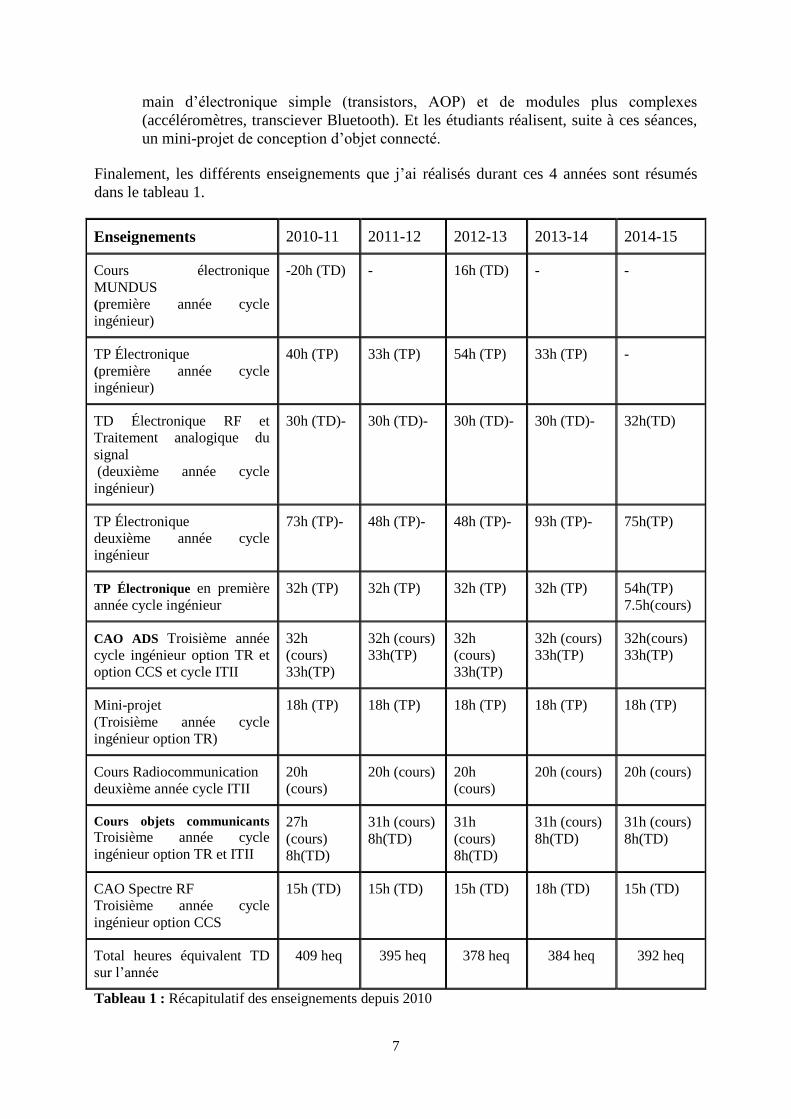
Finalement, les différents enseignements que j’ai réalisés durant ces 4 années sont résumés
dans le tableau 1.
Enseignements 2010-11 2011-12 2012-13 2013-14 2014-15
Cours électronique
MUNDUS
(première année cycle
ingénieur)
-20h (TD) - 16h (TD) - -
TP Électronique
(première année cycle
ingénieur)
40h (TP) 33h (TP) 54h (TP) 33h (TP) -
TD Électronique RF et
Traitement analogique du
signal
(deuxième année cycle
ingénieur)
30h (TD)- 30h (TD)- 30h (TD)- 30h (TD)- 32h(TD)
TP Électronique
deuxième année cycle
ingénieur
73h (TP)- 48h (TP)- 48h (TP)- 93h (TP)- 75h(TP)
TP Électronique en première
année cycle ingénieur 32h (TP) 32h (TP) 32h (TP) 32h (TP) 54h(TP)
7.5h(cours)
CAO ADS Troisième année
cycle ingénieur option TR et
option CCS et cycle ITII
32h
(cours)
33h(TP)
32h (cours)
33h(TP)
32h
(cours)
33h(TP)
32h (cours)
33h(TP)
32h(cours)
33h(TP)
Mini-projet
(Troisième année cycle
ingénieur option TR)
18h (TP) 18h (TP) 18h (TP) 18h (TP) 18h (TP)
Cours Radiocommunication
deuxième année cycle ITII
20h
(cours)
20h (cours) 20h
(cours)
20h (cours) 20h (cours)
Cours objets communicants
Troisième année cycle
ingénieur option TR et ITII
27h
(cours)
8h(TD)
31h (cours)
8h(TD)
31h
(cours)
8h(TD)
31h (cours)
8h(TD)
31h (cours)
8h(TD)
CAO Spectre RF
Troisième année cycle
ingénieur option CCS
15h (TD) 15h (TD) 15h (TD) 18h (TD) 15h (TD)
Total heures équivalent TD
sur l’année
409 heq 395 heq 378 heq 384 heq 392 heq
Tableau 1 : Récapitulatif des enseignements depuis 2010

8
ENCADREMENT DE THESE
Depuis 2010, j’ai eu l’opportunité de co-encadrer 7 thèses de doctorat, dont 6 ont été
soutenues.
Florian Canneva Titre de la thèse : "Antennes miniatures reconfigurables en fréquence, polarisation et
rayonnement"
Financement : Bourse Européenne
Date début : Oct. 2008 Date de soutenance : 8 Juin 2012 Encadrement : 30
%
Directeur de thèse : Robert Staraj 40 %, Co-encadrant : J-M Ribero 30%
Publications : J11MO-J11MO2-J13MO
Situation actuelle du diplômé : Ingénieur chez Ethertronics, Sophia Antipolis
Diane Titz Titre de la thèse : " Design and Characterization of Antenna-on-Chip and Antenna-in-
Package solutions for 60 GHz communications and beyond "
Financement : Bourse Normale
Date début : Oct. 2009 Date de soutenance : 20 Septembre 2012 Encadrement
: 30 %
Directeur de thèse : Cyril Luxey 40 %, Co-encadrant : Gilles Jacquemod 30%
Publications : J12MO-J12RE-J12AW-J12MO3-J12AM-J12AW3-J13AP-J13CP-
J13EL-J13AP3-J13AP4-J14MO-J14AW-J14AW3-J14CP-J14AW
Situation actuelle du diplômé : Professeur agrégé en CPGE au Lycée Jules
Ferry, Cannes
Oumy Diop Titre de la thèse : " Etude et Minimisation du Facteur de Qualité d’Antennes Miniatures
conçues pour de Petits Objets Communicants "
Financement : Bourse MESR
Date début : Oct. 2010 Date de soutenance : 27 Septembre 2013 Encadrement
: 30 %
Directeur de thèse : Cyril Luxey 40 %, Co-encadrant : Aliou Diallo 30%
Publications : C12IW2 C12SA
Situation actuelle du diplômé : Ingénieur chez Epcos-TDK à Sophia Antipolis
Marcio Silva Pimenta Titre de la thèse : " Antennes souples à bases de métamatériaux de type conducteurs
magnétique artificiels pour les standards de systèmes de géolocalisation "
Financement : Bourse ANR Metavest
Date début : Oct. 2010 Date de soutenance : 14 Novembre 2013 Encadrement
: 30 %
Directeur de thèse : Jean-Marc Ribero 40 %, Co-encadrant : Robert Staraj
30%
Publications : J12MO4
Situation actuelle du diplômé : Ingénieur chez Insight SIP à Sophia Antipolis
9
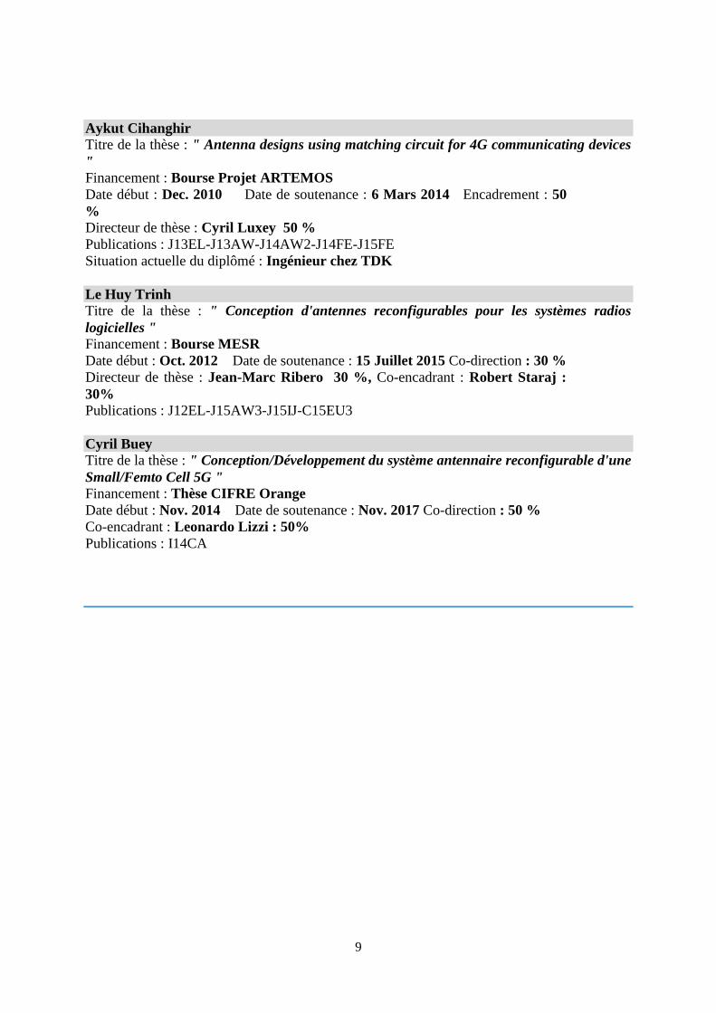
Aykut Cihanghir Titre de la thèse : " Antenna designs using matching circuit for 4G communicating devices
"
Financement : Bourse Projet ARTEMOS
Date début : Dec. 2010 Date de soutenance : 6 Mars 2014 Encadrement : 50
%
Directeur de thèse : Cyril Luxey 50 %
Publications : J13EL-J13AW-J14AW2-J14FE-J15FE
Situation actuelle du diplômé : Ingénieur chez TDK
Le Huy Trinh Titre de la thèse : " Conception d'antennes reconfigurables pour les systèmes radios
logicielles "
Financement : Bourse MESR
Date début : Oct. 2012 Date de soutenance : 15 Juillet 2015 Co-direction : 30 %
Directeur de thèse : Jean-Marc Ribero 30 %, Co-encadrant : Robert Staraj :
30%
Publications : J12EL-J15AW3-J15IJ-C15EU3
Cyril Buey Titre de la thèse : " Conception/Développement du système antennaire reconfigurable d'une
Small/Femto Cell 5G "
Financement : Thèse CIFRE Orange
Date début : Nov. 2014 Date de soutenance : Nov. 2017 Co-direction : 50 %
Co-encadrant : Leonardo Lizzi : 50%
Publications : I14CA

10
ENCADREMENT DE STAGES
Entre 2009 et 2015, j'ai participé à l’encadrement de 7 stages de niveau master 2 de 6 mois.
Le stage de Le Huy Trinh, Aiouaj Allal et Cyril Buey était financé par Orange dans le cadre
du CREMANT. Le stage d'Aimeric Bisognin était financé par l'équipe EpOC de l'Université
de Nice dans le cadre d'une collaboration sur la conception d'antennes millimétriques au sein
du CREMANT. Les autres stages étant financés par le LEAT.
Madiha El Khattab Titre du stage : " Antennes miniatures multistandards actives à base de nouveaux
matériaux et métamatériaux"
Financement : Fond propre LEAT
Date début : Fev. 2010 Date de fin : Juillet. 2010 Encadrement : 100%
Situation actuelle : Test Analyst chez Median Technology
Pauline Bouzat Titre du stage : " Conception d’une antenne combinée GPS / Iridium "
Financement : Fond propre LEAT
Date début : Fev. 2011 Date de fin : Juillet. 2011 Encadrement : 100%
Situation actuelle : Business analyst chez Amedeus
Le Huy Trinh Titre du stage : " Conception d'antennes reconfigurables pour les systèmes radios
logicielles "
Financement : Stage Orange
Date début : Fev. 2012 Date de fin : Juillet. 2012 Encadrement : 50%
Nom et % du co-encadrant: P. Brachat (50%)
Situation actuelle : Thèse MESR au LEAT
Aimeric Bisognin Titre du stage : " Conception et caractérisation de structures antennaires in-package pour
applications millimétriques WLAN indoor à 60GHz et 120GHz "
Financement : Fond propre EpOC
Date début : Fev. 2012 Date de fin : Juillet. 2012 Encadrement : 100%
Situation actuelle : Thèse ST Microéléctronique
Aiouaj Allal
Titre du stage : " Mise en place d’un banc de mesures MIMO 2x2 pour des applications
LTE "
Financement : Stage Orange
Date début : Avril. 2013 Date de fin : Aout. 2013 Encadrement : 50%
Nom et % du co-encadrant: J-P. Rossi (50%)
Situation actuelle : Ingénieur Télécoms à SIAE Montpellier
Cyril Buey Titre du stage : " Dimensionnement et évaluation d’un routeur à 8 antennes WiFi"
Financement : Stage Orange
Date début : Avril. 2014 Date de fin : Septembre. 2014 Encadrement : 50%
Nom et % du co-encadrant: J-P. Rossi (50%)
Situation actuelle : Thèse Orange

11
Zayd Ouachicha Titre du stage : " Mesure de système miniature à 868 MHz"
Financement : Stage CREMANT
Date début : Avril. 2014 Date de fin : Septembre. 2014 Encadrement : 100%
Situation actuelle : Ingénieur Sopra

12

13
Part 2 : Research activities
I will try in this part to retrace my research activities from the start of my PhD until now. I
will use this manuscript as an opportunity to disclose complimentary or un-published work.
I have started my research activity more than 10 years ago, and the writing of this HDR is
coming at the right time, when a flashback on your past research will help you to get into
position for the next 10 coming years.
My different research topics were mainly driven by Master and PhD student supervision, thus
i have divided the different section of this manuscript in relation with the students who were
involved in the studies.
In 2010, I was recruited on a "Maître de conference" position at the Polytechnic school of the
University of Nice Sophia-Antipolis to teach electromagnetics, Telecommunication and RF
microelectronics. I'm continuing my research activities within the "Laboratoire
d'Electronique, Antennes et Télécommunications (LEAT)" (Director is Jean-Yves Dauvignac)
in the CMA team (antenna design and modeling). An important part of my research presented
in this manuscirpt has been realized in colloboration with EpOC laboratory (Director is Gilles
Jacquemod). The majority of my work has been done in the frame of the CREMANT, joint
lab between University of Nice Sophia and Orange Company.
My research interests concerns the design and measurement of circuits and antennas for
telecommunication system. The first section of this part will be dedicated to my PhD studies
on the design of passive and active antennas. Then, I will present in the section II my research
work during my ATER position in 2008. My research as research engineer in IMRA Europe
Company will be described in the section III. In section IV will be dedicated to my Post-Doc
realized in the LEAT in the frame of the NAOMI ANR project in 2010.
The three last sections will be dedicated to my research studies as a "Maître de conference"
from 2011 in the frame of multiple MASTER and PhD studies that I Supervised or co-
supervised.

14
I. Introduction
From the past 20 years we have experienced a large change in people relationship, and
telecommunication technologies have been a key enabler of this evoluation.
The first industrial revolution began in Britain in the late 18th century, with the mechanisation
of the textile industry, printing and transportation using steam power. Tasks previously done
laboriously by hundreds hands were replaced by a single cotton mill: the factory was born.
Communication through journals and books enabled a mass alphabetization for the first time
in history. Public school in Europe and North America from 1830 to 1890 provided a skilled
workforce, able to lead complicated operation needed for the industry and railway
development based on steam power.
The second industrial revolution came in the early 20th century with electricity and
combustion engine. Electricity in factories and at home opened the mass production era. With
Henry Ford creating the moving assembly line, cars became accessible and the road network
spread in the countries. In a few decades, horses were replaced by cars in city and by tractors
in fields. New materials made from petrol appeared. Telephone lines, radio and television
changed the social life toward new communication models and trades.
The first two industrial revolutions made people richer and caused urbanization. A lot of
people consider that a third revolution is under way and, like all revolutions, it will be
disruptive.
A number of remarkable technologies are converging: digital systems, novel materials,
robotics, drones new fabrication processes, telecommunication, renewable energy and a whole
range of web-based services.
In my opinion, we can define four different sectors that are going to disrupt the world in this
third industrial revolution: Additive manufacturing, Robotics, Renewable energy and Digital
communication.
1. The Third revolution disruptive sectors
a) Additive manufacturing: 3D printing technology revolution
The factory of the past was dedicated to the fabrication of (x)illions of identical products: H.
Ford was used to say that car-buyers could have any colour they liked, as long as it was black.
Steve Jobs has allowed the consumer to choose between 5 colors, but inner material of an
IPhone is identical. We have seen with the automotive market (Citroen DS3, Fiat 500, Mini)
that the cost of producing much smaller batches of a wider variety, with each product tailored
to each customer's expectations, is now possible. The factory of the future will focus on mass
customization.
This revolution will change the way things are fabricated, but also where they are made.
Factories have moved to low-salary countries to drop labour costs. First labour costs have a
less and less important part in the final product cost: a $499 first-generation iPad included
only about $33 of manufacturing labour, of which the final assembly in China accounted for
just $8 [ECO12]. Production is going to move back to rich countries in order to have the
fabrication closer to the customers, to respond more quickly to changes in demand.

15
However, even if the production is going local, the design part will be completely digital and
the market will be worldwide. App Store and Android Market are the first exemple of
Worlwide open market directly connected to consumers.
3D printing is at an inflection point, and is about to shake most of the mainstream processes.
The first step of this technology was dedicated to prototyping, rapid tooling, trinkets, and
toys. But upcoming Additive manufacturing will create durable and safe products for sale to
real customers in moderate to large quantities. More and more materials can be used beyond
the classical ABS plastic, from ceramic [SCI16] to metal [ACC13].
Fig I.1 : 3D printing gears
b) Robotics : The Smart machines challenge
Boston Consulting Group has predicted that up to a quarter of jobs will be replaced by either
smart software or robots by 2025 [BBC15].
In France, Taxi drivers are actually fighting against Uber on-demand services, but a more
lethal threat is arriving with autonoumous car. Google announced in 2015 that their vehicles
have driven over 2,000,000 km without any traffic accident caused by the autonomous car.
Amazon plans to use unmanned aerial drones to deliver packages by air. Drones with 2.3 kg
package carrying capacity would be able to carry 83% of all of the items that Amazon
delivers.
In the manufacturing sector, most of the jobs will not be on the factory floor but in the offices
nearby, which will be full of designers, engineers, IT specialists, logistics experts, marketing
staff and other professionals. The manufacturing jobs of the future will require more skills.
Most of the repetitive tasks will become obsolete.
16
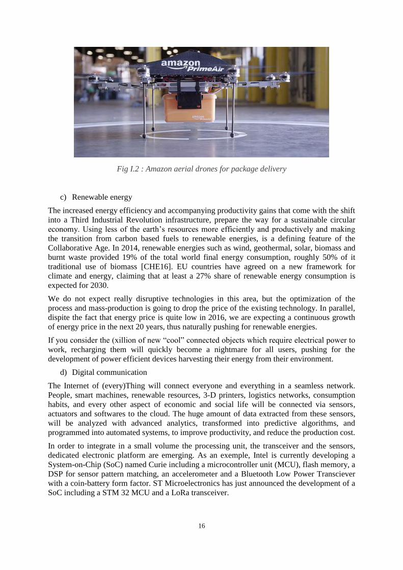
Fig I.2 : Amazon aerial drones for package delivery
c) Renewable energy
The increased energy efficiency and accompanying productivity gains that come with the shift
into a Third Industrial Revolution infrastructure, prepare the way for a sustainable circular
economy. Using less of the earth’s resources more efficiently and productively and making
the transition from carbon based fuels to renewable energies, is a defining feature of the
Collaborative Age. In 2014, renewable energies such as wind, geothermal, solar, biomass and
burnt waste provided 19% of the total world final energy consumption, roughly 50% of it
traditional use of biomass [CHE16]. EU countries have agreed on a new framework for
climate and energy, claiming that at least a 27% share of renewable energy consumption is
expected for 2030.
We do not expect really disruptive technologies in this area, but the optimization of the
process and mass-production is going to drop the price of the existing technology. In parallel,
dispite the fact that energy price is quite low in 2016, we are expecting a continuous growth
of energy price in the next 20 years, thus naturally pushing for renewable energies.
If you consider the (xillion of new “cool” connected objects which require electrical power to
work, recharging them will quickly become a nightmare for all users, pushing for the
development of power efficient devices harvesting their energy from their environment.
d) Digital communication
The Internet of (every)Thing will connect everyone and everything in a seamless network.
People, smart machines, renewable resources, 3-D printers, logistics networks, consumption
habits, and every other aspect of economic and social life will be connected via sensors,
actuators and softwares to the cloud. The huge amount of data extracted from these sensors,
will be analyzed with advanced analytics, transformed into predictive algorithms, and
programmed into automated systems, to improve productivity, and reduce the production cost.
In order to integrate in a small volume the processing unit, the transceiver and the sensors,
dedicated electronic platform are emerging. As an exemple, Intel is currently developing a
System-on-Chip (SoC) named Curie including a microcontroller unit (MCU), flash memory, a
DSP for sensor pattern matching, an accelerometer and a Bluetooth Low Power Transciever
with a coin-battery form factor. ST Microelectronics has just announced the development of a
SoC including a STM 32 MCU and a LoRa transceiver.

17
Fig I.3 : Intel wearable CurieTM electronic platform
This is the disruptive sector closer to my research topic and my perspectives will be largely
matched to the different need for efficient and smart IoT networks.
2. Research and Education perspectives
I can conclude that from an academic point of view, this (r)evolution is a fantastic opportunity
for research and education. Of course in this prospective view, telecommunication
technologies are in the heart of this revolution. Electromagnetic waves are essential to
suppress all the distance limits, to create smarter environments. Our future research has to
pave the way to this revolution. Due to the need of flexilility, support of multi-standard,
flexibile concept are needed.
On the education part, our teaching activity has also to evolve in order to give to the future
generation the required skills to accommodate themselves to this change. The impact of the
third revolution on learning will be profound. Any student has already infinitely more
information on any given subject with a simple click of a button than could ever be
disseminated by any teacher.
Therefore, we should shift from traditional notions of a teacher-student relationship, to one
with the responsibility on educators to facilitate flexible learning by becoming catalysts,
enablers and inspirers of this mass of information.
References
[ECO12] “The third industrial revolution”, The Economist, Apr 21st 2012
[SCI16] Additive manufacturing of polymer-derived ceramics, Zak C. Eckel, Chaoyin Zhou, John H. Martin,
Alan J. Jacobsen, William B. Carter, and Tobias A. Schaedler, Science 1 January 2016: 351 (6268), 58-62.
[ACC13] Anzalone, G.C.; Chenlong Zhang; Wijnen, B.; Sanders, P.G.; Pearce, J.M., "A Low-Cost Open-Source
Metal 3-D Printer," in Access, IEEE , vol.1, no., pp.803-810, 2013
[BBC15] Jane Wakefield “Intelligent Machines: The jobs robots will steal first”, BBC, Sept. 2015.
[CHE16] Nicola Armaroli, Vincenzo Balzani: Solar Electricity and Solar Fuels: Status and Perspectives in the
Context of the Energy Transition. In: Chemistry – A European Journal 22, (2016), 32-57,
doi:10.1002/chem.201503580.

18
II. PhD studies (2003-2007)
Just after my master thesis in Engineering diploma in 2003, Gilles Jacquemod, Full professor
at the University of Nice, proposed me to continue my studies through a PhD thesis funded by
the French government (MESR). The subject of my research was focused on reconfigurable
circuits and antennas. Under the supervision of Gilles Jacquemod, Robert Staraj, Cyril Luxey
from the LEAT, and Pr. Vincent fusco from the Queens University of Belfast, I had the task
to design reconfigurable antenna in polarization and directivity. I started my studies in
October 2003 and I defend my thesis the 19th of November 2007. The title and members of
my jury are stated below:
« Reconfiguration dynamique d’antennes imprimées en directivité et polarisation »
Pr Yann DEVAL, IMS de Talence, Président de jury
Pr Christian PERSON, GET/ENST de Bretagne, Rapporteur
Pr Philippe BENECH, IMEP ENSERG de Grenoble, Rapporteur
Mr Patrick PONS, LAAS de Toulouse, Examinateur
Mme Andreia CATHELIN, ST/Minatec de Grenoble, Examinateur
Pr Gilles JACQUEMOD, Université Nice Sophia-Antipolis, Directeur de thèse
Pr Robert STARAJ, Université Nice Sophia-Antipolis – LEAT, Responsable de thèse
Mr Cyril LUXEY, Université Nice Sophia-Antipolis – LEAT, Responsable de thèse
A. Motivation
The nineties have seen a rapid development of the mobile phone technology, in less than 10
years; a “wireless” revolution has established a new era in the telecommunication area.
Considering the constant increasing of wireless objects, features and data rates, more and
more complex technologies have to be integrated to support these developments. Fast-Fading
and shadowing effects in multi-propagating channel degrade strongly transmission signal to
noise ratio. To counter these parasitic effects, polarization and directivity diversity has been
proposed as shown on Fig. 1. Designing reconfigurable antenna is a major challenge and it
start with the development of active devices reliable, efficient, with low insertion loss and low
cost. Up to now, radiofrequency industry has mainly used semi-conductor device which are
able to meet most of customer needs. At the start of my PhD, micro mechanical system for
radiofrequency application was a very hot topic in the antenna community, and the high
potential of this novel technology was highly attractive. It was also full of sense to start this

19
activity at the LEAT at this time as this research topic was merging electromagnetic skills
with micro-electronic technology. Considering the increasing of carrier frequencies, and
linearity issues, these components (MEMS) offers interesting solutions (Fig. 1).
Utilisateurvisé
Utilisateurinterférant
(a) (b)
Fig. 1 (a) Directivity diversity applied to mobile phone, (b) Magfusion magnetic MEMS
Studies realized in this PhD concerns, on one hand, one the design and fabrication of efficient
RF MEMS device, on the other hand, on the design of antenna topology with suitability for
polarization and directivity reconfiguration.
B. Design of RF MEMS devices
The semi-custom MEMS processing MetalMUMPS PLUS from MEMSCAP Company was
selected because it was part of Europractice program. Some process problems were
encountered due to diffusion of the copper layer in the gold layer which created a dielectric
isolation between the gold and the polysilicon layer. The biasing of the MEMS electrodes was
not possible and therefore, only passive measurements were presented.
To perform minimum insertion loss for the phase shifter, we adopt switched line type
architecture. Each phase shifter is composed of two cascaded phase cell and each cell can
switch between three different delay lines. The key element of the phase shifters is then the
switch.
(a)
(b)
Fig. 2 (a)Mechanical simulation with Coventor, (b) Picture of a shunt MEMS (size 300*200 um2)

20
The movable membrane is made of a 2-μm thick polysilicon conductor layer placed between
two 0.35-μm thick silicon nitride layers and is situated under the 7-μm thick gold CPW lines.
This original topology was intended to simplify the packaging of the MEMS. The switches
are electro-statically actuated and use the upper silicon nitride layer as a dielectric. The
second silicon nitride layer allows polysilicon discontinuity on the same membrane.
Moreover, both silicon nitride layers ensure a perfect compensation of the residual stress in
the moveable structure. Two silicon dioxide layers are used as sacrificial layers. The
mechanical behavior of the structure was simulated with Coventor Software (Fig. 2). To
reduce actuation voltage, serpentine springs were used to connect the mobile membrane to the
substrate. The switches were design to have a collapsing voltage of Vc=24 V.
Photography of the MEMS switch using confocal optical sensor is proposed in Fig. 3. First
results for the MEMS are presented here. Fig. 3shows the results for the measurement and
simulation of the series type MEMS. The isolation between the two ports is higher than 25
dB. The return loss is measured to be better than -0.8 dB at 60 GHz. The level simulated are
quite close to the data measured. Measurements of the shunt MEMS are presented in Fig. 4.
The insertion loss is lower than 0.5 dB at 60 GHz and the return loss is lower than -20 dB at
60 GHz.
(a)
(b)
Fig. 3 (a) 3D scanning using confocal optical sensor of the series MEMS switch, (b) S11 and S21 for the series MEMS switch
(a)
(b)
Fig. 4 (a) S11 and S21 for the shunt MEMS switch, (b) 3D scanning using confocal optical sensor of rectangular slot antenna

21
A full beam-steering system including antenna and phase shifters was designed. In order to
have an array as compact as possible with minimal losses, the whole antenna is built using a
MEMS process. A photograph using confocal microscope is presented in Fig. 4. Thanks to the
short guided wavelength in Silicon at 60 GHz (λSi=1.46mm), it becomes possible to integrate
the whole MIMO array, including radiating elements and phase shifters, on a silicon die of
1cm². In order to direct the beam in only one direction, a metallic plane reflector is added
under the substrate. a CPW lines were used to reduce mutual coupling between closely spaced
lines. The final layout and a picture of a part of the antenna system is presented in Fig. 5. This
work was presented in [C06IC].
(b)
(a)
Fig. 5 (a) Layout of the beamforming antenna system, (b) Photograph with microscope
C. Reconfigurable hybrid coupler
For fifty years, considerable effort has been devoted to the study of tunable directional
couplers for reconfigurable microwave systems.
Our goal was to design a reconfigurable coupler able to alternatively provide the 3-dB Hybrid
mode (90° phase difference between the direct and the coupled port) or the uncoupled-line
mode (very low coupling between the direct and the coupled port). For this purpose, we
proposed the modification of a Quasi-Lumped Quadrature Coupler (QLQC) [FUS89]. A
frequency-tunable QLQC structure has been proposed in 1991 using ganged capacitors as the
vertical lines of a classical 3-dB hybrid circuit [FUS91]. For a given capacitance, this QLQC
is able to operate over a 5% bandwidth with adequate performance. When tuning the ganged
capacitors, the same 3-dB hybrid performance is maintained over a 120% bandwidth. This
foregoing research predicted a varactor diode implementation but such components with
suitable tunable capacitance values were not at that time available. However, such a QLQC
cannot meet our requirements; and further theoretical investigation is needed in order to
anticipate if the QLQC may be modified to achieve our operational requirements.
1. Theory and design of the tunable QLQC
The QLQC is a circuit with the vertical printed branches of a classic hybrid coupler are both
replaced by a lumped component with a suitable admittance. In this way the size of the

22
classical 3-dB hybrid can then drastically reduced. The structure consists of two parallel
horizontal transmission lines with characteristic impedance Z1 (Fig. 6). The complete analysis
of this structure has been presented in [J09MO].
Fig. 6 Schematic of a Quasi-Lumped Quadrature, QLQC, Coupler.
2. Tunable QLC and the uncoupled-line mode
In order to add some reconfigurability to this coupler, we substitute the lumped capacitors by
varactor diodes to get tuning capability versus DC bias. With a QLQC, the biasing circuit will
be really simple to implement thanks to the fact that the two horizontal transmission lines are
electrically isolated: one of these lines can be set to the high DC voltage while the other can
be forced to the DC ground. The analytical equations of the voltage amplitudes at port1 and
emerging trough port4 from port1 versus the admittance Y2 are given by (5). In addition, the
theoretical coupling ratio k versus the admittance is given by (6).
²)Y2Y21(jY21
²jYYAA
222
224111
(Equ.1)
²)YY(jY
²)YY1(jY1
A
Ak
222
222
31
21
(Equ.2)
The magnitude in dB and the phase of the coupling k as well as the matching at port 1
(magnitude of the S11 obtained by taking 20 log (equation 5) and the port4-to-port1 isolation
(same equation) are plotted versus the admittance (and thus the capacitor Chyb) in Fig. 7.a.
When the capacitance is tuned from 0.1*Chyb to 1.2*Chyb, k is varied from -3dB to +21dB and
the phase difference between S21 and S31 is maintained between 86° and 90°. At the same
time, the return loss and the isolation are both always higher than 15.5 dB. These curves
demonstrate that the QLQC can effectively operate as a quadrature tunable power splitter and
thus perform well for both the 3dB hybrid mode and the uncoupled-line mode at the same
frequency. A picture of the prototype is presented in Fig. 7.b.

23
(a)
(b)
Fig. 7 (a) Matching, coupling and output phase of the Quasi-Lumped Coupler when the capacitor is tuned, (b) Picture of the fabricated tunable QLQC
We measured this hybrid circuit at 3.5 GHz for reverse voltages Vr ranging from 0V to 15V
(Fig. 5). For capacitances lower than 0.2pF (Vr>11V), it can be seen that the four-port
network can be considered as two parallel uncoupled transmission lines. For a capacitance of
0.920 pF (Vr=0.96V), the system operates like a 3-dB hybrid coupler. In Fig. 8.a, we present
the simulated and measured Sij parameters versus frequency of the tunable QLC when
Vr=0.96V (3-dB hybrid mode). These curves are in very good agreement. The feeding signal
is evenly divided between port2 and port3 at 3.5 GHz. The return loss at port1 and the port4-
to-port1 isolation are both better than -25dB. In the uncoupled line mode (i.e. reverse voltage
equals to 15V), good isolation levels are obtained between port1-port3 and port1-port4 as well
as a good match. The insertion loss between port1-port2 is found to be -0.45dB at 3.5 GHz.
From this reference structure, cascaded structures were proposed to enhance bandwidth and
reconfigurability as shown in Fig. 8.b [J07EL]
(a)
(b)
Fig. 8 (a) S-parameters versus capacitance, (b) Cascade QLQC coupler
D. Application of reconfigurable couplers
24
Based on this reconfigurable microwave structure, we propose several antenna topologies for
polarization agility.
1. Quad polarization microstrip antenna
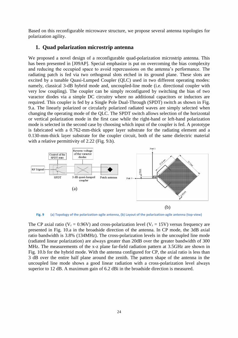
We proposed a novel design of a reconfigurable quad-polarization microstrip antenna. This
has been presented in [J09AP]. Special emphasize is put on overcoming the bias complexity
and reducing the occupied space to avoid repercussions on the antenna’s performance. The
radiating patch is fed via two orthogonal slots etched in its ground plane. These slots are
excited by a tunable Quasi-Lumped Coupler (QLC) used in two different operating modes:
namely, classical 3-dB hybrid mode and, uncoupled-line mode (i.e. directional coupler with
very low coupling). The coupler can be simply reconfigured by switching the bias of two
varactor diodes via a simple DC circuitry where no additional capacitors or inductors are
required. This coupler is fed by a Single Pole Dual-Through (SPDT) switch as shown in Fig.
9.a. The linearly polarized or circularly polarized radiated waves are simply selected when
changing the operating mode of the QLC. The SPDT switch allows selection of the horizontal
or vertical polarization mode in the first case while the right-hand or left-hand polarization
mode is selected in the second case by choosing which input of the coupler is fed. A prototype
is fabricated with a 0.762-mm-thick upper layer substrate for the radiating element and a
0.130-mm-thick layer substrate for the coupler circuit, both of the same dielectric material
with a relative permittivity of 2.22 (Fig. 9.b).
(a)
(b)
Fig. 9 (a) Topology of the polarization-agile antenna, (b) Layout of the polarization-agile antenna (top-view)
The CP axial ratio (Vr = 0.96V) and cross-polarization level (Vr = 15V) versus frequency are
presented in Fig. 10.a in the broadside direction of the antenna. In CP mode, the 3dB axial
ratio bandwidth is 3.8% (134MHz). The cross-polarization levels in the uncoupled line mode
(radiated linear polarization) are always greater than 20dB over the greater bandwidth of 300
MHz. The measurements of the x-z plane far-field radiation pattern at 3.5GHz are shown in
Fig. 10.b for the hybrid mode. With the antenna configured for CP, the axial ratio is less than
3 dB over the entire half plane around the zenith. The pattern shape of the antenna in the
uncoupled line mode shows a good linear radiation with a cross-polarization level always
superior to 12 dB. A maximum gain of 6.2 dBi in the broadside direction is measured.

25
(a)
(b)
Fig. 10 (a) Axial ratio in the hybrid mode and cross polarized level in the uncoupled line mode versus frequency of the antenna, (b) Measured CP radiation pattern of the antenna for Vr=0.96V at 3.5 GHz (3-dB hybrid mode)
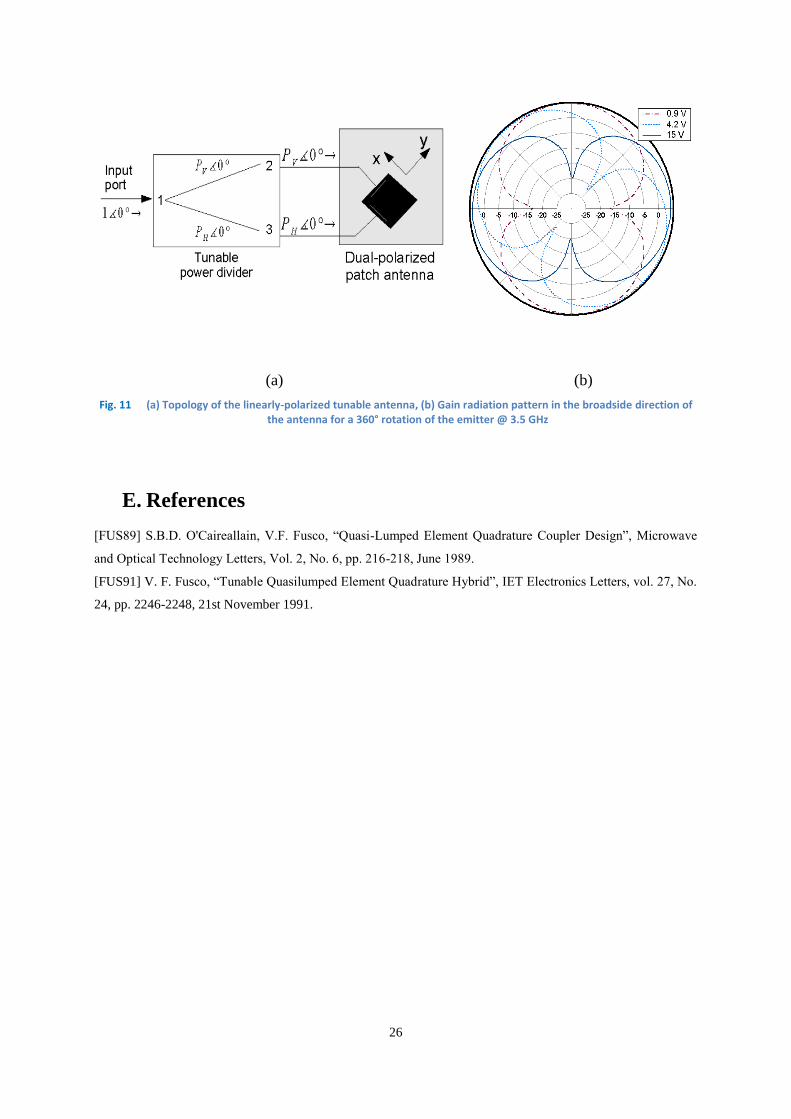
2. Linearly-Polarized Tunable Antenna
Many solutions have been investigated to rotate linear polarization without any mechanical
systems. Our proposed solution allows a dynamic rotation of the angle of the linearly-
polarised electrical field over a 90° angle: each direction can easily be achieved. It was
presented in [J11EL].
The principle of our antenna is shown in Fig. 11.a. Two orthogonal linearly-polarized
antennas are fed by a tunable power divider. The port 2 of the power divider is feeding the
vertically-polarized antenna with a power level PV (y direction). The port 3 of the power
divider is connected to the horizontally-polarized antenna with a power level PH (x direction).
By changing the power level of the outputs of the power divider, it is therefore possible to
change the rotation of the linearly-polarized wave over a 90° angle (Fig. 11.a). The phase
difference between the two outputs of the power divider has to be kept null to ensure a high
level of axial ratio i.e. high polarization purity. In addition, to keep the gain of the antenna
constant when changing the direction of the polarization, the addition of Pv and PH has to be
kept constant.
The gain radiation pattern in the normal direction of the antenna (broadside) for a 360°
rotation of the emitter is presented for three different voltages in Fig. 11.b. These
measurements show that a 93° rotation of the linearly-polarized wave is possible by changing
the reverse voltage from 0.9V to 15 V. During this rotation, the deviation of the gain in the
maximum direction is only ± 0.2 dB. Moreover, the cross-polarization level is kept higher
than 25 dB for all the different voltages.
26
(a) (b)
Fig. 11 (a) Topology of the linearly-polarized tunable antenna, (b) Gain radiation pattern in the broadside direction of the antenna for a 360° rotation of the emitter @ 3.5 GHz
E. References
[FUS89] S.B.D. O'Caireallain, V.F. Fusco, “Quasi-Lumped Element Quadrature Coupler Design”, Microwave
and Optical Technology Letters, Vol. 2, No. 6, pp. 216-218, June 1989.
[FUS91] V. F. Fusco, “Tunable Quasilumped Element Quadrature Hybrid”, IET Electronics Letters, vol. 27, No.
24, pp. 2246-2248, 21st November 1991.

27
III. Temporary assistant professor (ATER 2007-2008)
Following my PhD defense, I focused my work, in collaboration with Benjamin Nicolle who
was a PhD student at the LEAT, on high level modeling of complex system. Our objective at
the time was to develop a start-up able to propose engineering services for industrial project.
The modeling was based on VHDL-AMS modelling. This technique was applied to two
different areas: RF telecommunication and Biological system.
A. RF chain modeling using VHDL-AMS
Traditionally, analog and RFIC designers use a Bottom–Up design methodology based on the
use of elementary components (transistors, diodes, capacitors) in order to create electrical
functions. Then, these functions are assembled within more and more complex blocks until
the complete analog system design is reached. Thus, the obtained system is an association of
elementary blocks, generally described at the transistor level. The major disadvantage of this
description level is the extremely long simulation time that it takes to simulate the complete
system. It also makes difficult system verification because of the number of iteration needed
to find and correct an eventual error.
The efficiency of the Top–Down design flow depends directly on the performances of the
simulation environment. With systems becoming more complex and heterogeneous, the
ability of modeling both digital analog and RF parts within the same environment is of major
concern. For all those reasons, HDLs as Verilog-AMS and VHDL-AMS seem to offer good
mixed-signal capabilities and multi-abstraction level modeling solutions in order to optimize
the major phases of a complex system design flow. This study was focused on the advantages
of such a modeling solution compared to the generally used modeling habits, within the RFIC
design flow. A test case is proposed based on an RFIC satellite receiver design, and the non-
linear parameters are evaluated and compare with measurement as shown on Fig. 12. Results
show that the behavioral approach permits fast and accurate estimations (0.7 dB error average
for 8-channel composite-triplebeat inteference at 950MHz). This study was presented in
[J09MJ].
Fig. 12 CTB measurement on a RF chain

28
B. Virtual Skin model
The behavioural methodology was also applied to a very different area, a biological model of
the skin for sun burn prevention. VHDL-AMS allows to model discrete time behavior (as
VHDL) and continuous time behavior with differential algebraic equations (DAEs). Sunlight
(especially UVA penetrating deeper into the skin) has a profound effect on the skin causing
skin aging. We have been able to create a complex functional skin model and its environment
and to simulate it dynamically taking a part of the sunlight spectrum as the chain reaction
initiator. Therefore, we have divided the whole system in three blocks as explained figure 1
for complexity management purpose: sun UV spectrum, skin interaction and chemical
reactions in the skin (Fig. 13.a). We focused our study on the mitochondrial cell as it one of
the best-described entity in the literature. The previous generic sensitizer model has been
refined for Riboflavin species. When the excited sensitizer interacts with an oxygen, it creates
a reactive oxygen species (ROS) which can initiate a lipid chain reaction upon sun radiance.
Human skin defenses are included in the model as E vitamin, glutathione, etc. We
implemented as a first step, 96 chemical reactions using a 1st order approximation. We use a
species dictionary and a code generator based on chemical equations. Therefore, this model
can evolve easily to introduce more reactions. First results have confirmed assumption of a
lipid chain reaction in the skin initiated by the UVA radiance. 20 Ks real time was simulated
in 1 min on a standard PC. After 1Ks UVA radiance, the chain reaction initiates and we
measured a lipid half-lifetime of 14 Ks (Fig. 13.b). This result was very promising [C08HS]
and this work was continued by System VIP Company.
(a)
(b)
Fig. 13 (a) Virtual skin and its environment system architecture, (b) Lipid peroxidation simulation
29
IV. Research engineer in IMRA Europe SAS
I worked between September 2008 and September 2009 as a research engineer for IMRA
Europe SAS Company. IMRA is an advanced research center in signal processing, image
processing and solar cell. It is funded exclusively by the Japanese consortium Aisin Seiki,
parts manufacturer of Toyota. I work on several subjects during this year. A first part of my
study was focused on the measurement of field over a hybrid car body; a second was focused
on the design of integrated antenna for cars.
A. Hybrid car field measurement
Hybrid car exhibit a high level of interference which can corrupt RF receptor. The purpose of
this field measurement is to identify the frequency band which can propagate along the Prius
body and to find the main current path. 23 different points were measured on the Prius body
for electric and magnetic near-field. A spectrum analyser acquires data point between 500
KHz and 20 MHz. For the magnetic field, it was possible to estimate the direction of the
surface current by performing two orthogonal measurements on each point.
Thanks to these measurements, we indentify that a propagation channels was present on the
Prius body between 6 MHz and 15 MHz. The surface current is mainly flowing by the edge of
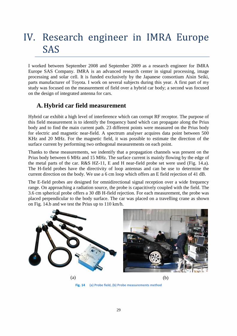
the metal parts of the car. R&S HZ-11, E and H near-field probe set were used (Fig. 14.a).
The H-field probes have the directivity of loop antennas and can be use to determine the
current direction on the body. We use a 6 cm loop which offers an E field rejection of 41 dB.
The E-field probes are designed for omnidirectional signal reception over a wide frequency
range. On approaching a radiation source, the probe is capacitively coupled with the field. The
3.6 cm spherical probe offers a 30 dB H-field rejection. For each measurement, the probe was
placed perpendicular to the body surface. The car was placed on a travelling crane as shown
on Fig. 14.b and we test the Prius up to 110 km/h.
(a)
(b)
Fig. 14 (a) Probe field, (b) Probe measurements method

30
The near field signal is amplified using a 38 dB gain preamplifier. A spectrum analyser
records the signal from 500 kHz to 20 MHz for each measure points. Then, measurements are
stored in a file with 501 different frequencies and the associated power measurement in dB
μV (Fig. 15.a). We intended with this analysis to understand the surface current path on the
car body. To help the understanding of this effect, a 3D Prius was modeled with the local
surface current value (Fig. 15.b).
(a)
(b)
Fig. 15 (a) H-field measurement versus frequency, (b) Surface current on Prius body @ 6MHz
Thanks to these measurements, we indentify that a propagation channels was present on the
Prius body between 6 MHz and 15 MHz. The surface current is mainly flowing by the edge
and the slot of the Prius body. The whip antenna is well isolated from these current. The
electric field is maximal on the slots of the body and exhibits some frequency peak close to
the whip antenna.From this measurement, we clearly understand that the next generation of
hybrid car will have to take into account electrical motor interference in the AM receptor
design.
B. Integrated antenna for cars
The main part of my activity in IMRA Europe was dedicated to antenna design for automotive
application. Antenna system are essential in automotive area to receive different
electromagnetic wavelengths as radio AM and FM, television, cellular phone, etc … Classical
solutions are the whip antenna mounted vertically on the vehicle. The radiation efficiency of
this type of structure is good (>70 %) but it reduce the aerodynamic characteristics and
obstruct the external appearance of the vehicle. The whip antenna can be broken and stolen,
moreover, it produce a wind break noise at high speed. Finally, this antenna has a reduced
bandwidth (<30% bandwidth with a return loss < - 6dB).
A second solution is the printed on screen window antenna. These antennas are integrated in
the vehicle and imply a low visual obstruction. However, due to their low metal thickness, the
efficiency is very low (<10 %) and active element as amplifiers are needed.
Last solution is to use small whip antenna (< 20 cm) with a matching active circuit. The whip
height reduction increases its impedance and worsens the obtainable bandwidth. To obtain
correct performances, active antenna principle is needed. The antenna feed point is directly
connected with an amplifier. This amplifier is optimized for a high input impedance in order
to pick up as much as possible from the antenna voltage and to act like an impedance
converter. The output of this amplifier is matched to 50 ohm and connected to the coaxial
31
cable. Antennas for automotive application have to support various bands which are described
in Tab. 1.
During my year in IMRA, we developped two different solutions for integrated antenna, and
the two topologies were patented. This first one was a wide band antenna integrated in the
spoiler of the car; the second one is a monopole with a shark fin shape placed in the top of the
roof.
Applications Europe (MHz) United State (MHz) Japan (MHz)
FM radio 88 - 108 88 - 106 70 - 90
DAB 174 - 237 88 - 106 470-770
TV 175 - 862 175 - 806 170 - 770
Car to car 5900 5900 700
WIFI 2400 - 5800 2400 - 5800 2400 - 5800
Cellular 900 – 1800 700-2170 810 - 2170
Tab. 1 Target applications with the UWB antenna
1. Spoiler antenna
Our proposal is to integrate the planar radiating element directly in non metallic part of the
vehicle like the air spoiler and the side mirror. This antenna combine a good efficiency
(>50%) in a large bandwidth (S11 < -6 dB on a band larger than one decade) and an invisible
shape. Air spoiler and mirror are usually made of thermoplastic resin, thus integration of
electromagnetic radiating element is possible.
Thanks to the size of the spoiler, usually at least 1 m wide and 20 cm length, it is possible to
integrate several antennas for spatial and directional diversity.
Currently, ultra-wide band technologies target applications in the 3.1 GHz to 10.6 GHz band
for pulse coded communication. Most recent applications target sensor data collection,
precision locating and tracking applications. To fulfil these specifications, specific antennas
have been developed with monopole and dipole structure. In addition to the ultra-wide band
capabilities, the radiation pattern of these antennas has to be omnidirectional as main
applications target mobile devices. Our proposal is to adapt the monopole concept developed
for the 3.1 GHz -10.6 GHz band in the 170 MHz-6 GHz band considering the vehicle body ,
this frequency bandwidth is valuable for the automotive applications (DAB, TV, cellular
phone, DSRC, WIFI, …). Concerning the FM radio, a modification of the UWB structure is
performed to enable the reception of the FM frequency band.
To cover the FM frequency band, a hole is etched in the monopole and a gap is created near
the feeding point. This hole and the gap form a bend monopole, to control the resonance
frequency of this bend monopole, a lumped capacitor is inserted in the gap (Fig. 16.a). The
capacitance controls the resonance frequency and the bandwidth can be tune on the FM
frequency band.

32
Fig. 16 Figure 1 : UWB antenna with hole and lumped capacitor
(a)
(b)
Fig. 17 (a) Integration of 3 UWB antennas in a air spoiler, (b) Return loss with and without the gap
To confirm the importance of the gap, a simulation is done with the hole but without the gap.
The simulation is presented on Fig. 16.b and show that no resonance appears in the low
frequency. This effect can be used to optimize the FM reception for the different country, as
shown on Tab. 1.
All presented antennas can receive and broadcast several automotive applications in several
part of the world as describe in table 1. A synthesis on the two original antennas, the UWB
antenna with the hole and the half UWB antenna with the hole, is presented on the Tab. 2.
Concerning the fabrication of this antenna and the integration with the spoiler, a metallic tape
(copper) with the shape of the antenna can be set on the spoiler before the painting.
Design parameters Europe United State Japan
Antenna 1 size (m²)
0.36*0.15 0.36*0.15 0.36*0.15
Lumped capacitor (pF) 60 60 87
Lumped capacitor
50 ohm port
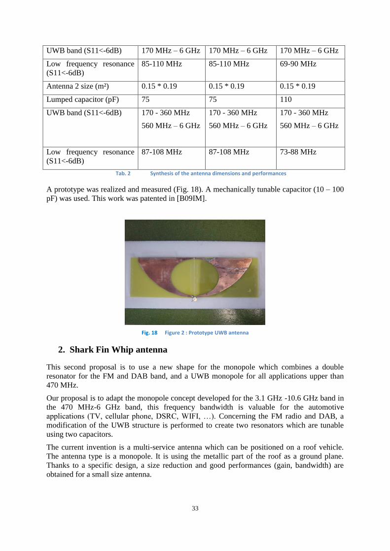
33
UWB band (S11<-6dB) 170 MHz – 6 GHz 170 MHz – 6 GHz 170 MHz – 6 GHz
Low frequency resonance
(S11<-6dB)
85-110 MHz 85-110 MHz 69-90 MHz
Antenna 2 size (m²) 0.15 * 0.19 0.15 * 0.19 0.15 * 0.19
Lumped capacitor (pF) 75 75 110
UWB band (S11<-6dB) 170 - 360 MHz
560 MHz – 6 GHz
170 - 360 MHz
560 MHz – 6 GHz
170 - 360 MHz
560 MHz – 6 GHz
Low frequency resonance
(S11<-6dB)
87-108 MHz 87-108 MHz 73-88 MHz
Tab. 2 Synthesis of the antenna dimensions and performances
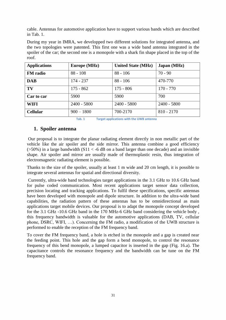
A prototype was realized and measured (Fig. 18). A mechanically tunable capacitor (10 – 100
pF) was used. This work was patented in [B09IM].
Fig. 18 Figure 2 : Prototype UWB antenna
2. Shark Fin Whip antenna
This second proposal is to use a new shape for the monopole which combines a double
resonator for the FM and DAB band, and a UWB monopole for all applications upper than
470 MHz.
Our proposal is to adapt the monopole concept developed for the 3.1 GHz -10.6 GHz band in
the 470 MHz-6 GHz band, this frequency bandwidth is valuable for the automotive
applications (TV, cellular phone, DSRC, WIFI, …). Concerning the FM radio and DAB, a
modification of the UWB structure is performed to create two resonators which are tunable
using two capacitors.
The current invention is a multi-service antenna which can be positioned on a roof vehicle.
The antenna type is a monopole. It is using the metallic part of the roof as a ground plane.
Thanks to a specific design, a size reduction and good performances (gain, bandwidth) are
obtained for a small size antenna.
34
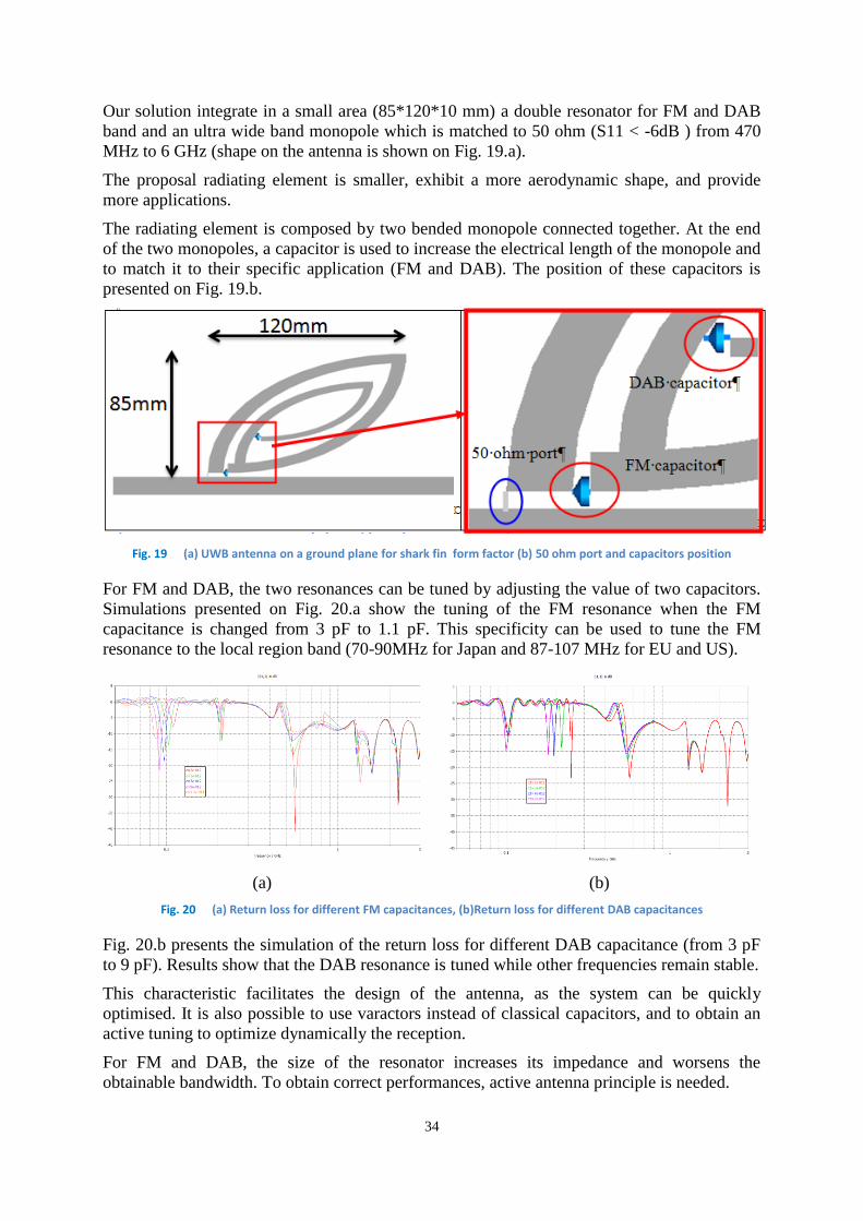
Our solution integrate in a small area (85*120*10 mm) a double resonator for FM and DAB
band and an ultra wide band monopole which is matched to 50 ohm (S11 < -6dB ) from 470
MHz to 6 GHz (shape on the antenna is shown on Fig. 19.a).
The proposal radiating element is smaller, exhibit a more aerodynamic shape, and provide
more applications.
The radiating element is composed by two bended monopole connected together. At the end
of the two monopoles, a capacitor is used to increase the electrical length of the monopole and
to match it to their specific application (FM and DAB). The position of these capacitors is
presented on Fig. 19.b.
Fig. 19 (a) UWB antenna on a ground plane for shark fin form factor (b) 50 ohm port and capacitors position
For FM and DAB, the two resonances can be tuned by adjusting the value of two capacitors.
Simulations presented on Fig. 20.a show the tuning of the FM resonance when the FM
capacitance is changed from 3 pF to 1.1 pF. This specificity can be used to tune the FM
resonance to the local region band (70-90MHz for Japan and 87-107 MHz for EU and US).
(a) (b)
Fig. 20 (a) Return loss for different FM capacitances, (b)Return loss for different DAB capacitances
Fig. 20.b presents the simulation of the return loss for different DAB capacitance (from 3 pF
to 9 pF). Results show that the DAB resonance is tuned while other frequencies remain stable.
This characteristic facilitates the design of the antenna, as the system can be quickly
optimised. It is also possible to use varactors instead of classical capacitors, and to obtain an
active tuning to optimize dynamically the reception.
For FM and DAB, the size of the resonator increases its impedance and worsens the
obtainable bandwidth. To obtain correct performances, active antenna principle is needed.
35
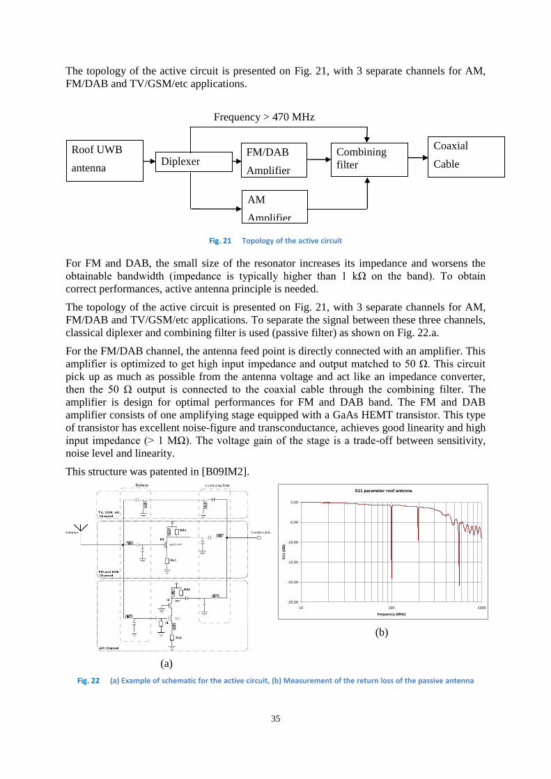
The topology of the active circuit is presented on Fig. 21, with 3 separate channels for AM,
FM/DAB and TV/GSM/etc applications.
Fig. 21 Topology of the active circuit
For FM and DAB, the small size of the resonator increases its impedance and worsens the
obtainable bandwidth (impedance is typically higher than 1 kΩ on the band). To obtain
correct performances, active antenna principle is needed.
The topology of the active circuit is presented on Fig. 21, with 3 separate channels for AM,
FM/DAB and TV/GSM/etc applications. To separate the signal between these three channels,
classical diplexer and combining filter is used (passive filter) as shown on Fig. 22.a.
For the FM/DAB channel, the antenna feed point is directly connected with an amplifier. This
amplifier is optimized to get high input impedance and output matched to 50 Ω. This circuit
pick up as much as possible from the antenna voltage and act like an impedance converter,
then the 50 Ω output is connected to the coaxial cable through the combining filter. The
amplifier is design for optimal performances for FM and DAB band. The FM and DAB
amplifier consists of one amplifying stage equipped with a GaAs HEMT transistor. This type
of transistor has excellent noise-figure and transconductance, achieves good linearity and high
input impedance (> 1 MΩ). The voltage gain of the stage is a trade-off between sensitivity,
noise level and linearity.
This structure was patented in [B09IM2].
(a)
S11 parameter roof antenna
-25,00
-20,00
-15,00
-10,00
-5,00
0,00
10 100 1000
frequency (MHz)
S1
1 (
dB
)
(b)
Fig. 22 (a) Example of schematic for the active circuit, (b) Measurement of the return loss of the passive antenna
Roof UWB
antenna
FM/DAB
Amplifier Diplexer
Combining
filter
Coaxial
Cable
Frequency > 470 MHz
AM
Amplifier

36
For AM channel, impedance matching is not needed due to the high external noise. AM
amplifier is built around a JFET cascode stage as shown of Fig. 22.a. JFET technology is used
as it presents a high immunity to flicker noise. Thanks to the cascode configuration, the Miller
effect upon the J1 transistor is avoided and a low input capacitance is provided. As for the
FM/DAB amplifier, the gain is a trade-off between sensitivity, noise level and linearity.

37
V. Postdoc on NAOMI project (ANR)
In September 2010, I started a one-year Post-Doc in the frame of NAOMI ANR project. The
main goal of the NAOMI project was the antenna miniaturisation using innovative material
for DVB-H application.
Digital video broadcasting for handheld terminal (DVB-H) is emerging as a new service for
mobile multimedia device. The operating frequency is ranging from 470 MHz to 702 MHz
(relative bandwidth 40 %). The free-space wavelength at the lower end is large (λ0=64cm)
compared to the typical size of handheld devices which implies to miniaturize the radiating
element. However, miniaturization of antennas is well known to reduce the bandwidth and to
decrease efficiency. DVB-H standard is based on the use of 8 MHz tunable narrow channels
selected over the whole DVB-H bandwidth. Narrow band tunable antennas have the potential
to exhibit higher efficiency, smaller size and lower return losses. The purpose of our study
was to develop small antennas placed on a 230*130mm² PCB ground plane for a tablet PC or
portable TV handset.
A. Tunable DVB-H antenna
1. Design
For this type of application, the size of the screen occupies the main part of the chassis and
only a small volume can be dedicated to antennas. As folded monopole structure was chosen
for its good tradeoff between bandwidth, size and efficiency, a small clearance zone in the
corner of the PCB (30 *8 mm²) is realized. The monopole (total length 12 cm) is folded in a
2.7 mm3 volume (30*8*8). A view of the antenna is given on Fig. 23. The antenna center
frequency without the varactor diode is 979 MHz. Monopole usually exhibits an impedance of
33 Ω at the resonance frequency. However, when the internal monopole antenna is placed
closer to the PCB, the resistive part of the antenna impedance collapses. In our study, using
HFSS microwave EM simulator, the resistive part of the impedance is found to be equal to 9
Ω, which is rather small. To add some tunability on the resonance frequency, a varactor diode
is positioned between the top of the monopole and its basis. To simplify the study, an
analytical model is determined. An equivalent series resonance circuit can be used to model
the monopole antenna behavior. The varactor diode is modeled using a capacitor and a
resistor in series. The varactor diode is shunting a large part of the resonator inductance (3/4)
and a small part of the resistance (1/10). These ratios were determined by fitting the simulated
curves with the circuit model using Agilent ADS simulator. An equivalent circuit model of
the whole radiating structure is proposed on Fig. 24.a. However, due to the small resistive part
of the impedance, a matching circuit is also required. The matching circuit is implemented by
using an open stub which is more convenient to match a series resonator on a wide band. The
stub is placed closed to the ground plane as shown in Fig. 23. The Smith chart for a varactor
capacitance of 2.35 pF for several lengths of the stub is presented in Fig. 24.b. Comparison is
made between the model and the EM simulation and a good agreement is found. Optimum
stub has to match the antenna on all the DVB-H coverage. As bandwidth is narrower at low
frequency, stub length has to be chosen to enlarge the -10 dB bandwidth at 474 MHz. The
optimal bandwidth is obtained for a length of 29.4 mm.

38
2. Prototype and experimental results:
A prototype was realized. The bended monopole was fabricated in nickel silver using
micromachining technique. The monopole is then soldered on the FR4 substrate. A surface-
mount GaAs hyperabrupt varactor from MACOM (MA46416) was used. A 50 Ω-microstrip
line across the ground plane is used for the RF feeding and for the DC biasing of the varactor.
As the monopole is folded on itself, a 100 pF capacitor acting as a DC block and an RF short
circuit is introduced in the metallic strip just after the varactor, allowing a part of the
monopole to be DC isolated. This part is then connected to the DC ground potential by using
a thin line including a choke inductor to block the RF signal. The details of the biasing circuit
are shown on the Fig. 23.
Return loss measurements of the antenna with varactor reverse bias voltages between 2.5V
and 10.5V are presented in Fig. 25.a. The operating frequency was continuously tuned over
the DVB-H band. Concerning the bandwidth, the narrowest -6 dB return loss bandwidth
(10MHz) was measured at 470 MHz. At 700 MHz, the bandwidth was 20 MHz. Thus, the
antenna fulfils the DVB-H specifications. The efficiency of the antenna was measured using
Wheeler cap method [WHE59]. A metallic box of 23*23*40 cm3 was used to perform
measurements. Fig. 25.b presents the simulated and measured efficiency and DVB-H
specification for 5 different frequencies. A good agreement is found between the EM
simulation and the Wheeler cap method. Due to cavity mode in the Wheeler cap, efficiency
measurement for frequency higher than 650 MHz was not possible but simulation shows that
efficiency continue to increase. Thus, a comfortable safety margin is obtained from ETSI
specifications. This work was presented in [J10MO].
Fig. 23 Antenna geometry
(a)
(b)
Fig. 24 Equivalent circuit, (b) Smith chart comparison

39
(a)
(b)
Fig. 25 (a) S11 for 5 different voltages, (b) Simulated and measured efficiency
B. Magneto-Dielectric Tunable UHF Antenna
The second part of my Post-Doc was focused on the use of Magneto-Dielectric material for
antenna miniaturization. Compared to high permittivity dielectric, high permeability materials
have the capability to reduce the size of the antenna without decreasing the relative bandwidth
and total efficiency [SOU10]. However, such magneto-dielectric material get higher losses
than classical substrate, thus an accurate study has to be realized to quantify the real impact of
such resonators on miniature antenna. This work was presented in [J10AW].
1. Magneto-dielectric material
The purpose of our study was to develop small antennas placed on a 230*130mm² PCB
ground plane for a tablet PC or portable TV handset. In this work, a new iteration of magneto-
dielectric material used in [SOU10] and [PIN10] was implemented. Thanks to a hot isostatic
pressing technique, the average magnetic losses were reduced by a ratio of 13 % on the DVB-
band. To evaluate the interest of this material, two different antennas were designed with and
without the magneto-dielectric resonator. Two separate prototypes have been realized and
measured to compare their radioelectric performances.
(a)
(b)
Fig. 26 (a) Magneto-dielectric porous ceramic, (b) Picture of antenna B prototype
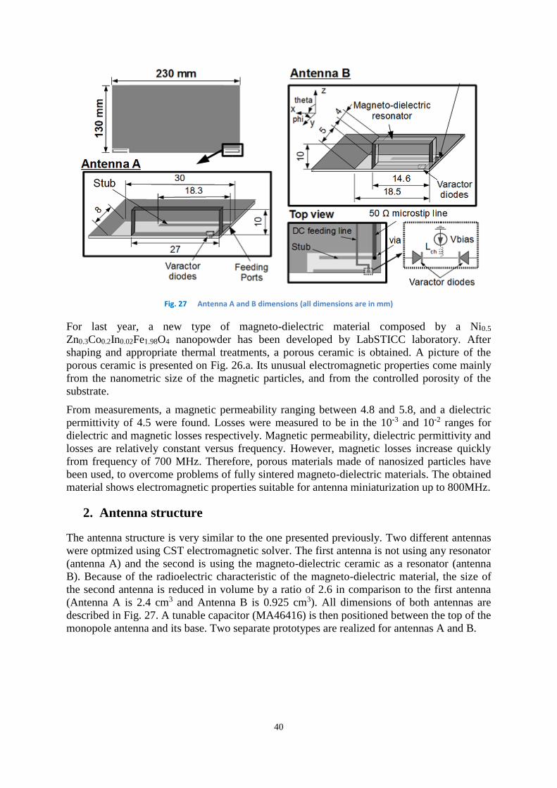
40
Fig. 27 Antenna A and B dimensions (all dimensions are in mm)
For last year, a new type of magneto-dielectric material composed by a Ni0.5
Zn0.3Co0.2In0.02Fe1.98O4 nanopowder has been developed by LabSTICC laboratory. After
shaping and appropriate thermal treatments, a porous ceramic is obtained. A picture of the
porous ceramic is presented on Fig. 26.a. Its unusual electromagnetic properties come mainly
from the nanometric size of the magnetic particles, and from the controlled porosity of the
substrate.
From measurements, a magnetic permeability ranging between 4.8 and 5.8, and a dielectric
permittivity of 4.5 were found. Losses were measured to be in the 10-3 and 10-2 ranges for
dielectric and magnetic losses respectively. Magnetic permeability, dielectric permittivity and
losses are relatively constant versus frequency. However, magnetic losses increase quickly
from frequency of 700 MHz. Therefore, porous materials made of nanosized particles have
been used, to overcome problems of fully sintered magneto-dielectric materials. The obtained
material shows electromagnetic properties suitable for antenna miniaturization up to 800MHz.
2. Antenna structure
The antenna structure is very similar to the one presented previously. Two different antennas
were optmized using CST electromagnetic solver. The first antenna is not using any resonator
(antenna A) and the second is using the magneto-dielectric ceramic as a resonator (antenna
B). Because of the radioelectric characteristic of the magneto-dielectric material, the size of
the second antenna is reduced in volume by a ratio of 2.6 in comparison to the first antenna
(Antenna A is 2.4 cm3 and Antenna B is 0.925 cm3). All dimensions of both antennas are
described in Fig. 27. A tunable capacitor (MA46416) is then positioned between the top of the
monopole antenna and its base. Two separate prototypes are realized for antennas A and B.

41
3. Measurements
Return loss measurements of antennas A and B versus frequency for varactor reverse bias
voltages varying between 1.2V and 10.5V are presented in Fig. 28.a. The operating frequency
was continuously tuned over the DVB-H band. Measurements show that for both antennas,
resonance frequencies correspond to the same reverse voltage on the varactor diodes, thus
they add equivalent losses to both antennas. Concerning the bandwidth, the narrowest -6 dB
return loss bandwidth (9MHz) was measured at 474 MHz for antenna A. Despite the fact that
antenna B is smaller than antenna A, antenna B has a wider bandwidth for all the different
voltages. At 850 MHz, -6 dB return loss bandwidth is 50 MHz for antenna A and 80 MHz for
antenna B. This effect is mainly due to the losses in the magneto-dielectric material, and the
bandwidth enlargement is greater at higher frequencies where magnetic losses are stronger.
Eventually, both antennas fulfill the return loss DVB-H specifications. Radiation
measurements were performed on a Stargate-24 measurement station with SATIMO facilities.
Measured directivity and realized gain are presented for both antennas on Fig. 28.b.
Directivity for both antennas is quite similar on the DVB-H band and naturally increases with
frequency. However, the directivity remains low on the DVB-H band (< 5 dB). Furthermore,
the gain is lower for antenna B compare to antenna A. At 470 MHz, the gain of Antenna A is
1.8 times larger the gain of Antenna B, while the volume ratio between them is 2.6. These
results confirm that magneto-dielectric material can help to maintain a correct efficiency
when the size of the antenna is reduced. However, the gain difference between both antennas
increases versus the frequency (2.6 dB @ 470 MHz and 4.2 dB @ 860 MHz) which confirms
that losses in magneto-dielectric material increase with frequency. The European
Telecommunications Standards Institute (ETSI) recommends a gain of -10dB at 470 MHz
[ETS05], and this specification is respected for both antennas.
C. References
[SOU10] D. Souriou, J. L. Mattei, S. Boucher, A. Sharaiha, A. C. Tarot, A. Chevalier, P. Queffelec: "Antenna
Miniaturization and Nanoferrite Magneto-Dielectric Materials", ANTEM 2010, Ottawa, July 2010.
[PIN10] J.-F. Pintos, A. Louzir, P. Minard, J. Perraudeau, J.L. Mattei, D. Souriou, P. Queffelec, “Ultra-Miniature
UHF Antenna using Magneto-dielectric Material”, ANTEM 2010, Ottawa, July 2010.
[WHE59] H. A. Wheeler, “The radiansphere around a small antenna,” Proceedings of the IRE, vol.47, pp. 1325-
1331, August 1959.
(a)
(b)
Fig. 28 (a) Return loss for antennas A and B for different reverse voltages, (b) Gain and directivity of antenna A and B versus frequency

42
[ETS05] “Digital Video Broadcasting (DVB), DVB-H Implementation Guidelines”, ETSI TR 102 377 v1.2.1,
Nov. 2005.

43
Research activities as " Maître de conférences" (2010-2014)
I was recruited in October 2010 as a "Maître de conferences". I've divided my research
activities into three main parts: the first one concern the design reconfigurable antenna in
UHF band. The second part is dedicated to the optimization of miniaturized, multi-band and
multi-antenna system, and the last part deals with design and characterization of millemeter
waves communcation systems.

44
VI. Reconfigurable antenna
From the really beginning of my research career, I’ve been strongly involved in
reconfigurable activity. First, because I’ve a strong background in electronic and micro-
electronic and it was obvious for me to try to mix my education with my research topic.
Secondly, when I start my PhD, MEMS for RF was at the really beginning, and there was a
feeling in the antenna community that this new type of component was going to revolution the
antenna market. 10 years after, MEMS are still an interesting axis of research, but no
successful application to massmarket has been demonstrated so far. Then, most of my work
has been done using PIN diodes and varactors, and more recently CMOS Digital Tunable
Capacitor (DTC).
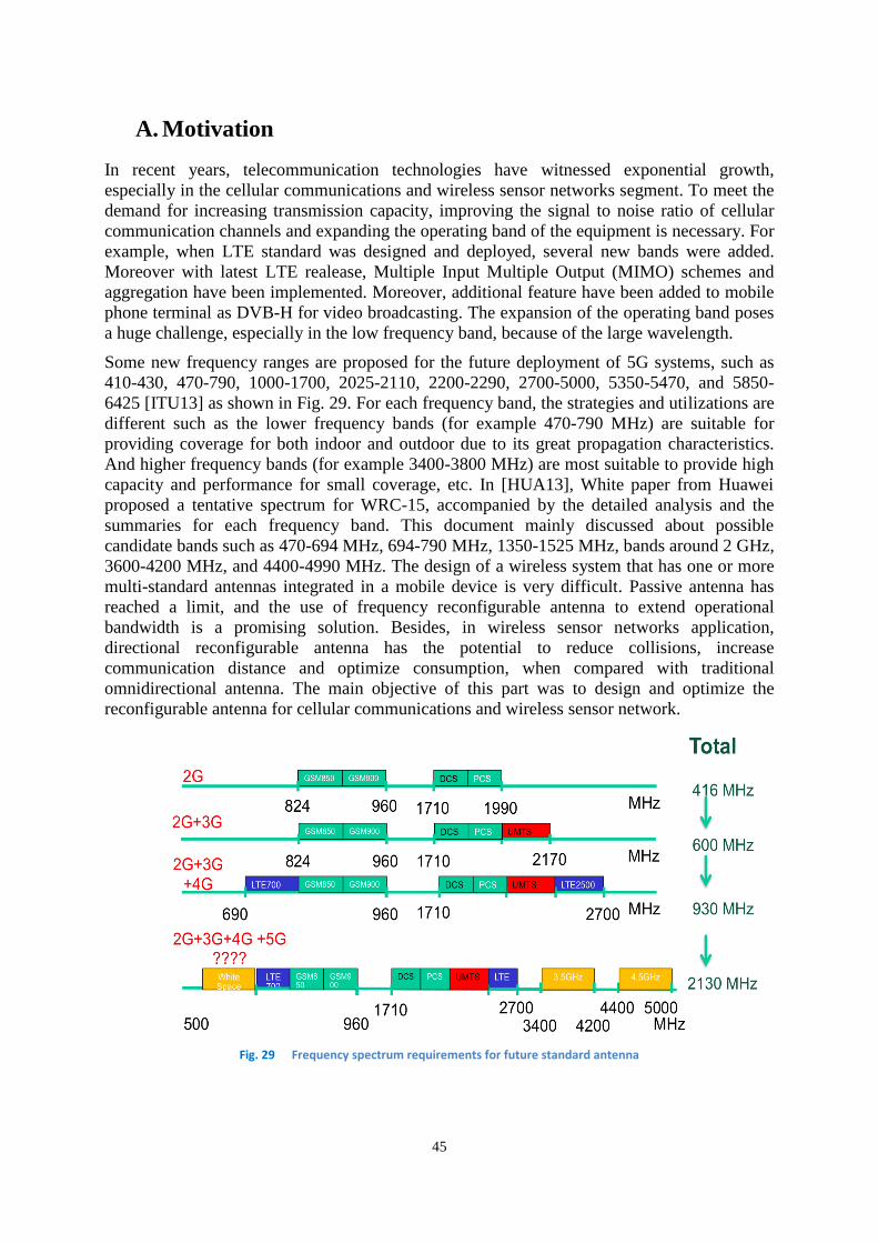
45
A. Motivation
In recent years, telecommunication technologies have witnessed exponential growth,
especially in the cellular communications and wireless sensor networks segment. To meet the
demand for increasing transmission capacity, improving the signal to noise ratio of cellular
communication channels and expanding the operating band of the equipment is necessary. For
example, when LTE standard was designed and deployed, several new bands were added.
Moreover with latest LTE realease, Multiple Input Multiple Output (MIMO) schemes and
aggregation have been implemented. Moreover, additional feature have been added to mobile
phone terminal as DVB-H for video broadcasting. The expansion of the operating band poses
a huge challenge, especially in the low frequency band, because of the large wavelength.
Some new frequency ranges are proposed for the future deployment of 5G systems, such as
410-430, 470-790, 1000-1700, 2025-2110, 2200-2290, 2700-5000, 5350-5470, and 5850-
6425 [ITU13] as shown in Fig. 29. For each frequency band, the strategies and utilizations are
different such as the lower frequency bands (for example 470-790 MHz) are suitable for
providing coverage for both indoor and outdoor due to its great propagation characteristics.
And higher frequency bands (for example 3400-3800 MHz) are most suitable to provide high
capacity and performance for small coverage, etc. In [HUA13], White paper from Huawei
proposed a tentative spectrum for WRC-15, accompanied by the detailed analysis and the
summaries for each frequency band. This document mainly discussed about possible
candidate bands such as 470-694 MHz, 694-790 MHz, 1350-1525 MHz, bands around 2 GHz,
3600-4200 MHz, and 4400-4990 MHz. The design of a wireless system that has one or more
multi-standard antennas integrated in a mobile device is very difficult. Passive antenna has
reached a limit, and the use of frequency reconfigurable antenna to extend operational
bandwidth is a promising solution. Besides, in wireless sensor networks application,
directional reconfigurable antenna has the potential to reduce collisions, increase
communication distance and optimize consumption, when compared with traditional
omnidirectional antenna. The main objective of this part was to design and optimize the
reconfigurable antenna for cellular communications and wireless sensor network.
Fig. 29 Frequency spectrum requirements for future standard antenna

46
B. DVB-H reception system
This study has been done in the frame of Florian Canneva PhD and ANR NAOMI project. I
start to supervise this work during my Post-doc, and i simply continue it with my MCF
position. Jean-Marc Ribero was the main supervisor and Robert Staraj contributes to this
study. This research worked was dedicated to frequency reconfigurable antenna using PIN
diodes or Varactor diodes. Many solutions were developed during this PhD, I will focus on
two different work: a PIFA reconfirable antenna and an active system for improvement of
antenna isolation.
1. Reconfigurable PIFA
The antenna consists in a Printed-Inverted-F-Antenna (PIFA) of dimensions 30x30 mm2, 5
mm above a printed circuit board of dimensions 230x130 mm2. The geometry of the structure
and its position on the ground plane is given on Figure 1. The antenna is loaded by a varactor
diode, connected to the upper metallic plate by a 3-mm width metallic strap of also 2-mm
height, which will allow to choose the desired channel in the DVB-H band. Indeed, as the
frequency behavior of the PIFA can be modeled by a RLC shunt resonator, by changing the
capacitance C the varactor diode allows to select the desired resonance frequency. The RF/DC
decoupling of the reverse bias voltage applied to the varactor is obtained by a slot etched in
the ground plane. An extra 100 pF CSM capacitor is placed across the slot to increase its
capacitance and to keep the antenna matched. The ground plane is designed on a 0.8-mm
thick FR4 substrate with a dielectric permittivity er = 4.7. Dimensions and position of the
decoupling slot are shown on Fig. 30. The width of the slots is 0.2 mm. This work was
preented in [J11MO2]
To simulate the varactor diode, a simplified equivalent circuit made up of a resistor in series
with a variable capacitor was used. Return losses for different values of the capacitor have
been simulated using Ansoft high frequency structure synthesizer (HFSS) solver. A prototype
has been realized using a surfacemount GaAs hyperabrupt varactor from MACOM
(MA46416). For reverse biasing voltage values Vb from 0 to 20 volts, the varactor diode
capacitance varies from 6 to 0.6 pF. Simulation and measurements for four different biasing
voltages of the varactor are given on Fig. 31.a. Measurements agree with the simulation. As
we can see, for a biasing voltage between 1.55 and 8.06 V, the proposed radiating element
reaches to cover the whole DVB-H band, with for each frequency, a _10- dB bandwidth equal
or superior to 8 MHz. Simulations of the efficiency have been done for four different
frequencies (474,590, 690, and 874 MHz) using HFSS electromagnetic simulator.
Furthermore, the efficiency satisfies the specification required for the DVB-H standard. For
example, radiation efficiency, total efficiency and return loss at the lower channel of the
DVB-H standard, (channel 34, from 470 to 478 MHz) are given in Fig. 31.b. In this channel,
the total efficiency is upper than 25%, whereas the specification is only 10%.

47
Fig. 30 Antenna geometry
(a)
(b) Fig. 31 (a) Measurements and simulations of the return losses for different bias voltage, (b) Measurement of S11,
total efficiency, and radiation efficiency at 474 MHz
2. Active system for improvement of antenna isolation.
A modified version of the previous antenna was used in this study. Two PIFA have been
placed on a ground plane of 100*60 mm2. It has been shown that the performance of the
antennas can be improved by a good coupling with the ground plane. Then, to have the best
electromagnetic performance than we can we place the antennas at the position given Fig.
32.a.

48
(a)
(b)
Fig. 32 (a) Position of the resonator on the PCB, (b) Active neutralization line
The Fig. 32.b presents position and dimensions of the active neutralization line. The principle
is to use a line to change the equivalent impedance between the two ports and then to reduce
the transmission throw. Unfortunately this technique is too narrow band to cover the band
needed for the DVB-H standard. By changing the value of the equivalent capacitor of the
varactor, we will change the equivalent impedance between the two ports. The varactor
choose in order to decoupling the two antennas in the wanted frequency range is the MACOM
46418 which has a range of equivalent from 3 to 0,3 pF for a bias voltage from 1 to 9 V. To
decoupling the RF/DC tension, we use SMD (Surface Mounted Device) stock inductance of
4,7 μH and lying capacitor of 100 nF.
The system has been realized using micro-machining techniques. The S parameters of
antennas have been measured for different configurations at 400 and 500MHz. Measurements
have been also compared with simulation in each case. Fig. 33 a & b represent respectively
the S parameters of the system when the antennas work at 400 MHz in a non-optimal case (a)
and in an optimal case (antennas are well-matched and decoupled). In the first case, the bias
voltage for antennas 1 and 2 are respectively 1,11 V and 1,63 V and the varactor on the
neutralization line is not biased. For the second case, the bias voltage for antennas 1(V1) and 2
(V2) are respectively 1,11 V and 1,56 V and the bias voltage for the neutralization line Vbias is
4.2 V. By adapting the neutralization line we reduce the S21 from -7.5 to -27 dB.
We can easily observe that, by adjusting the good bias voltage and so adjusting the good value
of the equivalent capacitance of the varactor, we can dramatically reduce the coupling
between the two elements. Furthermore, the reduction of the coupling between the two
antennas improve the matching of it. Then the S11 decreases from -7 to -22 dB. Fig. 34 a and b
show respectively the results of the measurement that have been done for other working
frequencies, when the antennas resonate at 506 MHz when the line is not biased (V1 = 2.06 V,
V2 = 2.34 V, Vbias = 0V) and when the line is optimized ( V1 = 1.96 V, V2 = 2.22 V, Vbias =
5,6 V). The adjustment of the bias voltage reduces the S21 from -9 dB to-35 dB and S11 from -
5 dB to -17 dB.
We can observe a small difference between measurements and simulations. This should be
due to the biasing wire. Indeed at low frequency the wave length is more important, then, in

49
spite of the decoupling RF/DC component using, the wire will have an influence on an
influence on input impedance. In addition, the technical datasheet of varactors claim an error
on the value of the capacitance of 10%.
(a)
(b)
Fig. 33 Measured S parameters when the two antennas work at 400 MHz for the case the reconfigurable line is not optimized (a) and the reconfiguration line is well-optimized (b)
a
(a)
(b)
Fig. 34 Measured S parameters when the two antennas work at 500 MHz for the case the reconfigurable line is not optimized (a) and the reconfiguration line is well-optimized (b)
C. Tunable Antenna designs using MEMS switch for 4G
communicating devices
This study was realized in the frame of the ARTEMOS project, whose objective whose main
target is to design tunable architectures for the RF front ends in future mobile handheld
terminals. This work was realized in the frame of Aykut Cihanghir PhD, under the main
supervising of Cyril Luxey and Gilles Jacquemod. This study was presented in [C13LA]
With the introduction of the fourth generation (4G) of cellular mobile communications, there
has been an increase in the frequency bands that a generic mobile phone should be able to
operate. This requirement poses some challenges in the design of the transceiver modules of
the device as well as the RF front-end and the antenna.
From the antenna design point of view, the newly added frequency bands especially LTE
bands 12-13-17 which goes down to 700MHz creates the main design challenge: covering

50
700-960MHz (30% bandwidth) in the low-band, considering also backward compatibility
with the former technologies like GSM850/900. Since the space reserved for the antenna is
electrically small in this frequency range and tends to decrease, special design techniques are
necessary to obtain the required bandwidth for a generic mobile terminal antenna.
In this work, a reconfigurable designs for 4G coverage in mobile terminals have been
proposed. Different antenna topologies are evaluated consisting of tunable antennas as well as
single/multi-feed structures.
1. MEMS switch component
With the new functionalities continuously being added to mobile handheld devices, the
necessity of covering more and more frequency bands from the antenna design perspective
has arisen. Since the dimensions of the space reserved for the antenna has been kept almost
the same although the necessity to be more broadband and also with the introduction of the
LTE frequency bands going down to 700MHz, the challenge has even become harder for the
antenna designer. One of the methodologies to overcome this challenge is using
reconfigurable (or tunable) antennas using tunable components like MEMS switches. This
components can be used directly in the antenna structure (for example to tune electrical length
of a strip) as well as at the antenna feed to tune the input impedance. An antenna design using
a MEMS switch was realized to switch between the operating bands, which are selected as
low-band (LB; 700-960MHz) and high-band (HB; 1.7-2.7GHz).
The MEMS switches that are to be used are designed and manufactured by DELFMEMS
[DEL13].
The mechanical principle is based on two main innovations: the fact the movable membrane
has no anchors and that both states are forced states. The membrane used for the electro-
mechanical function is an anchorless membrane. It is just simply supported over two pillars so
the degree of freedom are not the same compared to classical cantilevers (clamped-free
membrane) or bridges (clamped-clamped membrane) based structures. Two sets of electrodes
combined with two pillars create a lever effect which enables a push pull effect.
Fig. 35 (a) Schematic view of the two forced states, (b) SEM view of a SPST cell including 3 SPST
On state and off state are performed respectively when internal or external set of electrodes is
actuated as illustrated Fig. 35.a, on state is provided when internal actuation is performed
(voltage applied on inner electrodes); forced OFF state is provided when external actuation is
performed (voltage applied on outer electrodes). The main drawback of such design is that a
dual command is necessary in order to properly drive the device. A SEM view of the SPST
cell is presented in Fig. 35.b.

51
Insertion loss (IL) was measured on several devices with values at 2GHz between 0.25dB and
0.28dB and below 0.42dB at 5GHz (Figure 3.a). One of the major contributors to the insertion
loss is the parasitic capacitance created by the horizontal feed-through when crossing the
sealing ring of the packaging. For the next run the width of the sealing ring will be highly
reduced thus decreasing the capacitance. Hence, the IL will be automatically
decreased.Concerning the reflection coefficient, a matching below 15dB is obtained up to
5GHz.
2. Reconfigurable Antenna Design
The antenna design use MEMS component for band-switching between the LB and HB. The
antenna excitation methodology is based on the selection between two driven strips. The
proposed antenna layout can be seen in Fig. 36.a. The antenna is directly printed on the FR4
substrate having dimensions of 115mm X 60mm X 0.8mm, with a ground clearance of 15mm
for the antenna. The antenna consists of two driven strips, one for LB coverage and one for
HB coverage. To increase the bandwidth potential in the LB, a parasitic element (printed
under the substrate) was again used, which is capacitively excited by the LB driven strip and
connected to the ground plane over an SMD inductor (18nH) on the other end. The inductor
used in the ground connection helps to increase the electrical length of the parasitic strip, thus
arranging the resonance frequency created by the parasitic strip. One SPDT MEMS switches
is used to direct the excitation current either through the LB path or the HB path as seen in
Fig. 37.a. When the LB driven strip is excited, the parasitic strip is also capacitively excited,
enabling a higher bandwidth potential in the LB.
Fig. 36 Simulation Model of Tunable Antenna (General View) and soldering of the MEMS Switch using bonding wires
The S-parameter measurements of this prototype could be measured both with real MEMS
devices and with passive prototypes. In passive measurements, to represent the ON state of
the MEMS, a simple wire was soldered bypassing the MEMS and the connection was left
open to represent the OFF state. The measured reflection coefficient for the antenna in the LB
and HB states can be seen in Fig. 37.b. The target bands can be covered with a reflection
coefficient below -6dB in both passive measurements and measurements with real MEMS
devices, using the band-switching topology. Simulations are also presented and a good
agreement is observed with measurement.

52
Fig. 37 (a) Swith chart and Currents on the Antenna for Different Frequencies, (b) Simulated Reflection Coefficient with the Switchable MN
The total efficiency of the antenna was also measured (for passive prototypes only, due to
reliability issues) for LB and HB cases and presented in Fig. 38.There is an efficiency of
higher than -3dB except around 700MHz in the LB and an efficiency higher than -2.5dB in
the HB.
Fig. 38 Measured Total Efficiency for Antenna Design I
D. Reconfigurable antenna for extension of lte operational
mode over tv white spaces
This part presents a reconfigurable antenna for mobile terminal and TV white space
communications, using a Digitally Tunable Capacitor (DTC). This study was realized in the
frame of Trinh Le Huy PhD, J-M Ribero was the main supervisor, and Robert Staraj
collaborates to this work.
The antenna structure is matched permanently over the high frequency bands including
DCS/PCS, UMTS, LTE 1800/2600, and 3.5GHz bands. Concerning the sub-GHz bands,
several reconfigurable states enable a full coverage of LTE 600/700 and GSM 850/900
standards, as well as future applications on TV White space (TVWS). With dimensions of
40×10×6 mm3 for the antenna and 130×70×0.8 mm3 for the whole PCB, this structure can be
easily integrated in any mobile terminal.

53
As tunable component, CMOS DTC are used, it combines high power handling (34 dBm),
low power consumption (150 A) and a good capacitance scale (7.7:1) in a compact
packaging. It is controlled with I2C or SPI protocol and has 32 different states [DTC15]
1. Antenna design
The geometry of the proposed antenna (Fig. 39) is based on the capacitive coupling principle
between a fed monopole and parasitic elements. The antenna has a compact design (40 mm
×10 mm × 6 mm) and it is placed on top of a FR4-Epoxy substrate with a size of 130 mm ×
70 mm × 0.8mm, relative permittivity 4.4, and loss tangent 0.02.
Fig. 39 The geometry of proposed antenna and chassis dimension.
The proposed antenna consists of three different elements (Fig. 39). The center element is a
meandered monopole fed by a 50Ω microstrip line (orange). The monopole has an overall
length of about 84 mm, which creates a resonance around 900 MHz. In the middle of this
branch, two strips (pink) are used to provide two resonances at 1750 MHz and 3500 MHz.
Moreover, the shunt capacitance effect between the meander monopole and the shorted
parasitic element (yellow) generates an additional resonance for the lower band. By tuning the
dimension of the “coupled part” (red), the impedance matching in the low-band can be
optimized. This shorted parasitic element is connected to the ground plane through a variable
capacitor. By tuning its capacitance CTot, a narrow band can be reconfigured to cover the 630-
860 MHz frequency range. On the right side, a ground strip (blue) is used to cover the 2.5
GHz band. Finally, a new resonance is obtained at 2.7 GHz thanks to an optimization of the
shape of the meander monopole. The combination of these two different solutions enables the
correct matching of the antenna over the middle frequency band. The simulated reflection
coefficient for different capacitance is presented in Fig. 40 for (a) low band and (b) high band.
Fig. 40 simulated reflection coefficient (a) LB (b) HB

54
2. Results and discussion
The VSWR curves in the lower frequency bands are presented in Figure Fig. 40.b. When the
capacitance value of DTC is tuned between 0.6 pF to 1.8 pF, the reflection coefficient of the
antenna is modified. For the 0.6pF capacitance, a bandwidth a 100 MHz between 860 MHz
and 960 MHz is obtained. For higher capacitance values, a narrow band with a 3:1 VSWR can
be tuned from 600 MHz to 850 MHz with an instantaneous bandwidth always higher than 10
MHz. This modification has a small impact on the high frequency band, and the antenna is
constantly matched between 1.6 GHz to 2.7 GHz and 3.3 to 3.6 GHz with a 3:1 VSWR (Fig.
40.b).
Figure Fig. 41 shows the prototype of the proposed antenna. The unwrapped radiating
structure shown in Figure 3.24 has been printed on the FR4 substrate and successively folded
thanks to the mechanical milling of the edges to be bent. The tunable capacitor used to
reconfigure the antenna is the Peregrine PE64905 DTC. On the back of the PCB, an I2C
system used to control the DTC is placed. It consists of a Mbed NXP LPC 1768
microcontroller and three AA batteries which are placed in the holder. In shunt configuration,
the DTC can provide capacitance values from 0.9 pF to 5.6 pF (measured values).
Consequently, in order to achieve the needed 0.61 pF capacitance value (Fig. 40.a), a series
capacitor Cs = 1.9 pF is connected to the DTC. The resulting measured capacitance values
(CTot=CDTCCs/(CDTC+Cs) as well as the bandwidths of the antenna obtained in the different
DTC configurations are summarized in Table 3.1. As it can be noticed, the antenna enables
continuous coverage with high frequency resolution control in the low band.
Fig. 41 The fabricated prototype and the control unit.
DTC State CDTC (pF) CTot (pF) BW (MHz) DTC State CDTC (pF) CTot (pF) BW (MHz)
0 0.90 0.61 790-980 16 3.35 1.21 663-680 1 1.29 0.77 760-840 17 3.49 1.23 660-677 2 1.42 0.81 742-805 18 3.63 1.25 657-673 3 1.56 0.86 734-792 19 3.80 1.27 655-670 4 1.70 0.90 725-778 20 3.94 1.28 652-667 5 1.83 0.93 721-762 21 4.08 1.30 650-664 6 1.96 0.96 716-751 22 4.26 1.31 647-661 7 2.10 1.00 710-740 23 4.39 1.33 645-659 8 2.24 1.03 704-730 24 4.54 1.34 643-656 9 2.37 1.05 697-721 25 4.68 1.35 641-654
10 2.59 1.10 690-713 26 4.85 1.37 639-652 11 2.65 1.11 683-705 27 4.99 1.38 638-650 12 2.78 1.13 677-698 28 5.13 1.39 636-648
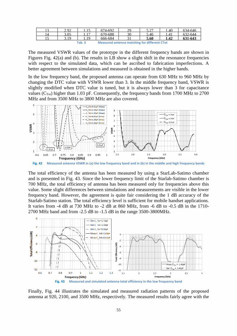
55
13 2.92 1.15 674-692 29 5.27 1.40 634-646 14 3.05 1.17 670-688 30 5.46 1.41 632-644 15 3.19 1.19 666-684 31 5.60 1.42 631-643
Tab. 3 Measured antenna matching for different CTot
The measured VSWR values of the prototype in the different frequency bands are shown in
Figures Fig. 42(a) and (b). The results in LB show a slight shift in the resonance frequencies
with respect to the simulated data, which can be ascribed to fabrication imperfections. A
better agreement between simulations and measured is obtained in the higher bands.
In the low frequency band, the proposed antenna can operate from 630 MHz to 960 MHz by
changing the DTC value with VSWR lower than 3. In the middle frequency band, VSWR is
slightly modified when DTC value is tuned, but it is always lower than 3 for capacitance
values (CTot) higher than 1.03 pF. Consequently, the frequency bands from 1700 MHz to 2700
MHz and from 3500 MHz to 3800 MHz are also covered.
Fig. 42 Measured antenna VSWR in (a) the low frequency band and in (b) in the middle and high frequency bands
The total efficiency of the antenna has been measured by using a StarLab-Satimo chamber
and is presented in Fig. 43. Since the lower frequency limit of the Starlab-Satimo chamber is
700 MHz, the total efficiency of antenna has been measured only for frequencies above this
value. Some slight differences between simulations and measurements are visible in the lower
frequency band. However, the agreement is quite fair considering the 1 dB accuracy of the
Starlab-Satimo station. The total efficiency level is sufficient for mobile handset applications.
It varies from -4 dB at 730 MHz to -2 dB at 860 MHz, from -6 dB to -0.5 dB in the 1710-
2700 MHz band and from -2.5 dB to -1.5 dB in the range 3500-3800MHz.
Fig. 43 Measured and simulated antenna total efficiency in the low frequency band
Finally, Fig. 44 illustrates the simulated and measured radiation patterns of the proposed
antenna at 920, 2100, and 3500 MHz, respectively. The measured results fairly agree with the

56
HFSS simulation. The radiation behavior at the different frequencies is quasi-omnidirectional,
thus being suitable for mobile terminal scenarios.
Fig. 44 Simulated (dotted line) and measured (solid line) radiation pattern of the proposed antenna
E. References
[ITU13] TU-R Joint Task Group, “Annex 3 to joint task group 4-5-6-7 chairman’s report working document
towards preliminary draft CPM text for WRC- 15 agenda item 1.1,” Tech. Rep. Document 4-5-6-7/393-E, Oct.
30, 2013.
[HUA13] Huawei. (2013, February). Whitepaper On Spectrum [Online]. Available:
http://www.huawei.com/ilink/en/download/HW_204545
[DEL13] Delfmems, http://www.delfmems.com/
[DTC15] Peregrine Semiconductor Corp., “UltraCMOS Digitally Tunable Capacitor (DTC) 100-3000 MHz”,
Document No. 70-0335-06, 2012.

57
VII. Multi-band and miniature antenna
From the start of telecommunication history, antenna designer have tried to miniaturize
radiating elements, because antenna are always too large. Being an antenna designer is really
complicated task, considering that nobody want to add any cents for the antenna, but the
specification and bands are always increasing, thus leading to impossible tradeoff. This
consideration can explain the constant decrease of the antenna performance reflection
coefficient criteria (-6dB of reflection coefficient in mobile phone). Moreover, new
applications for wireless connectivity as biomediacal or wearable system require antenna
miniaturization. Moreover, in order to maintain acceptable radiation efficiency, isolation
techniques from humain body impact are needed.

58
A. Motivation
The popularity of small communicating objects as mobile phones are become a
mainstream is today life. However, more and more standards are needed to be covered in a
unique terminal, leading to the development of multi-band and wide band communication
device.
A fundamental and intrinsic parameter of an electrically small antenna is its Quality
Factor (Q), which is defined as the ratio of 2π times the energy stored in the near fields
excited by the antenna to the energy radiated plus dissipated per cycle. The potential
bandwidth of an antenna is inversely proportional to its quality factor, which results in low
bandwidth potential for a high-Q antenna. The lowest obtainable radiation quality factor can
be calculated from Equ. 3 which is known as the Chu limit for electrically small antennas.
(Equ.3)
where k is the wavenumber (2π/λ) and a is the radius of the smallest sphere that can enclose
the antenna. It is necessary to note that this value is an optimistic theoretical value considering
a linearly polarized antenna radiating only in one (TE or TM) mode.
(Equ.4)
The obtainable frequency bandwidth can be calculated from Equ. 4 as also presented in
[HOL11], where S is the maximum target VSWR and T is the coupling coefficient as given in
[PUE89]. For a value of T=1, Equ. 4 reduces to:
(Equ.5)
This situation is called the "critically coupled" case, where the input impedance of the
antenna is matched exactly to Z0 (generally 50Ω) at a single frequency point.
For the calculation of the Q-factor of an antenna from its input impedance, Equ. 6 was
proposed in [YAG05], which proposes a fast and reliable calculation method.
(Equ.6)
with ω being the angular frequency point, R(ω) and X(ω) stands for the real and imaginary
parts of the impedance at angular frequency ω, and R'(ω) and X'(ω) are the first derivates of
R(ω) and X(ω) according to the frequency. This formula is valid for a single resonant antenna
close to its resonance frequency but it has proven reliable performance so far.

59
B. Antenna miniaturization for bio-medical applications
This work was realized in the frame of Oumy Diop PdD, under the main supervision of Cyril
Luxey and supervision of Aliou Diallo. When I join this PhD, it was already in progress and i
do not participate to the first study on miniaturisation limits, but i contribute to the second part
on the design and fabrication of small antenna. This second axis was focused on 2.4GHz
antenna for biomedical implant and handheld device. Several configurations were studied and
fabricated using various type of technology. Especially IPD process, which has the potential
to co-integrate antenna and RF circuit, was studied.
Communicating objects in the 2.4 GHz ISM band are becoming smaller and smaller, then
entire radiofrequency front-ends need to be co-integrated to miniaturize and optimize the
performance. A further improvement consists in co-designing those two elements in terms of
impedance conjugate match. Today transceiver solutions are mainly integrated on monolithic
silicon using system-on-chip technology. However, some parts of the system cannot be
integrated as silicon technology exhibits a low quality factor for inductors, baluns and
circulators and therefore low performance. The IPDTM process developed by
STMicroelectronics Tours [STM12] has been especially created to design lossless passive
devices like resistors, capacitors or inductors. Therefore, designs of passive circuits (baluns,
transformers), diplexers and filters UHF frequency already on the market, show a promising
trend for this IPDTM process [CHI11-ART11]0. A co-integration of the active circuit and a
circulator or a transformer has been presented in [SHI11] but the antenna was still an external
component on the Printed Circuit Board (PCB). However, the IPD technology is also
potentially highly interesting for a full integration of the passive front-end including the
antenna device.
A simplified side view of the BEOL of this process in presented in Fig. 45.a. This study is of
special interest as IPDTM technology from ST Microelectronics, Tours has been fully
characterized in the ISM band, and offer very high quality factor for inductors in this
frequency band.
Glass Substrate
εr≈4.6
Oxyde
Oxyde
εr≈2.7
M1
M2
M3
Vias
400 µm
0.5 µm0.8 µm
6 µm
3 µm
≈ 25 µm
6 µm
6 µm
Ubm
Fig. 45 (a) IPDTM Process build-up (not to scale), (b) Co-Integration of the active and passive circuits

60
Moreover, antenna directly integrated in silicon would have a very low efficiency and will
increase hardly the cost of the final solutions. An elegant solution is to obtain a good trade-off
between integration and performance in realizing the front-end passive circuit using the IPD
technology. A schematic example of this integration scheme is shown in Fig. 45.b with
circulator, balun, filter and antenna integrated on a IPDTM susbtrate.
To connect the transceiver (RFIC) and the IPD, several solutions exists as wire bonding and
solder bumps. In the second case, the IPDTM superstrate is flip-chipped on the PCB. In the ST
technology, two bump diameters are available, 140 µm and 240 µm, respectively called micro
and macro bumps. We choose here to use the macro bumps to enhance the matching
bandwidth. The general AiP strategies developed and presented in Fig. 46 has the potential to
deliver a low-cost solution for 2.4GHz communication.
Fig. 46 Direct integration of the antenna and the RFIC into the PCB using the IPD process.
1. Balun on IPD technology
As a proof-of-example, a miniature balun has been designed to transform a 50 ohm single port
to a 30 ohm differential port. The transformer integrated on the IPD technology use the M2
and M3 copper levels. The layout of the structure is presented in Fig. 47.a and a very small
size of 420*420um2 is obtained.
Fig. 47 (a) Balun transformer on IPDTM, (b) Simulated scattering parameters of the balun with Port single impedance of 50 ohm and Port Diff impedance of 30 ohm
S-parameter simulation using ADS simulator and ST design kit are presented in Fig. 47.b. An
0.7 dB insertion loss is obtained on the 2.4 GHz band and the reflection coefficient is lower
than -20dB on this entire band.
2. Single ended 2.4 GHz antenna on IPD technology
A monopole antenna using a thin meander line of 50 um width is presented in Fig. 48.a. The
antenna is realized with the M2 and M3 copper layer to decrease the resistivity of the line.
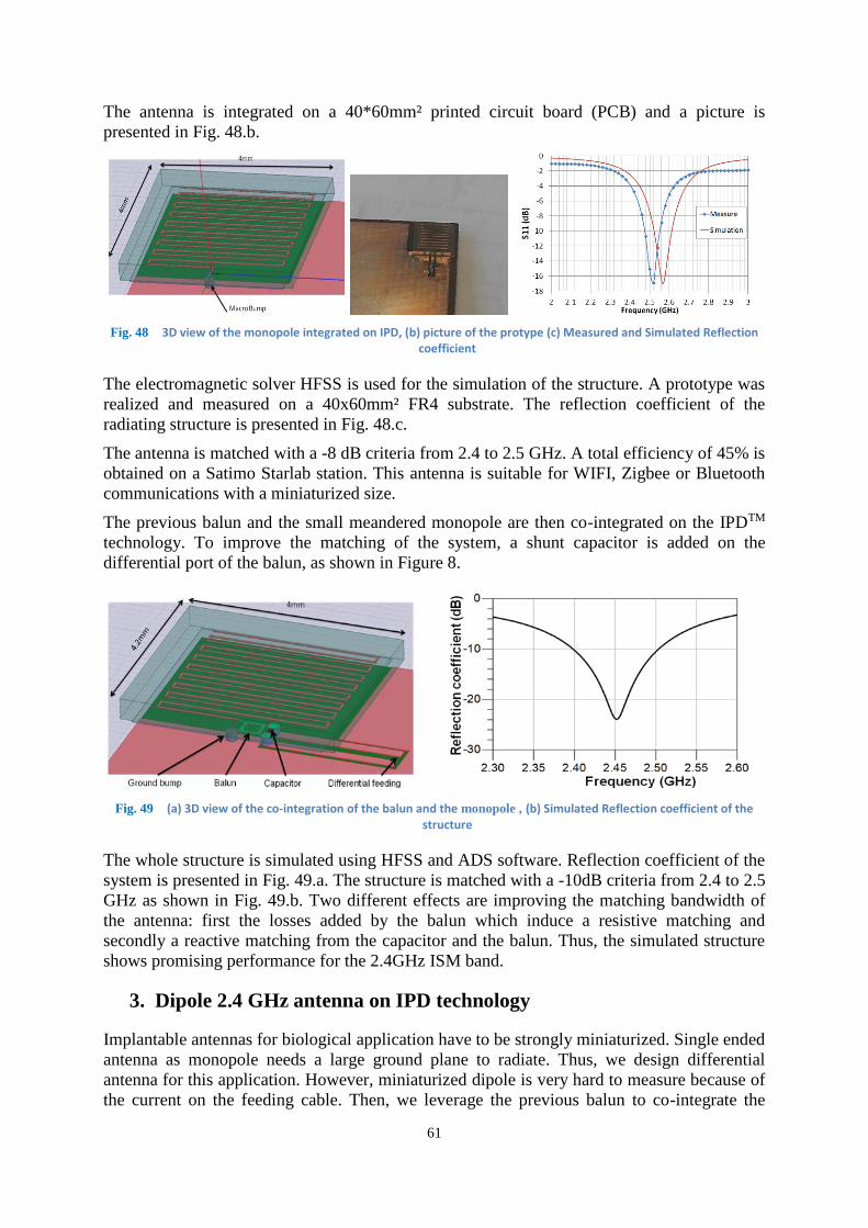
61
The antenna is integrated on a 40*60mm² printed circuit board (PCB) and a picture is
presented in Fig. 48.b.
Fig. 48 3D view of the monopole integrated on IPD, (b) picture of the protype (c) Measured and Simulated Reflection coefficient
The electromagnetic solver HFSS is used for the simulation of the structure. A prototype was
realized and measured on a 40x60mm² FR4 substrate. The reflection coefficient of the
radiating structure is presented in Fig. 48.c.
The antenna is matched with a -8 dB criteria from 2.4 to 2.5 GHz. A total efficiency of 45% is
obtained on a Satimo Starlab station. This antenna is suitable for WIFI, Zigbee or Bluetooth
communications with a miniaturized size.
The previous balun and the small meandered monopole are then co-integrated on the IPDTM
technology. To improve the matching of the system, a shunt capacitor is added on the
differential port of the balun, as shown in Figure 8.
Fig. 49 (a) 3D view of the co-integration of the balun and the monopole , (b) Simulated Reflection coefficient of the structure
The whole structure is simulated using HFSS and ADS software. Reflection coefficient of the
system is presented in Fig. 49.a. The structure is matched with a -10dB criteria from 2.4 to 2.5
GHz as shown in Fig. 49.b. Two different effects are improving the matching bandwidth of
the antenna: first the losses added by the balun which induce a resistive matching and
secondly a reactive matching from the capacitor and the balun. Thus, the simulated structure
shows promising performance for the 2.4GHz ISM band.
3. Dipole 2.4 GHz antenna on IPD technology
Implantable antennas for biological application have to be strongly miniaturized. Single ended
antenna as monopole needs a large ground plane to radiate. Thus, we design differential
antenna for this application. However, miniaturized dipole is very hard to measure because of
the current on the feeding cable. Then, we leverage the previous balun to co-integrate the

62
differential antenna with it, and make it easier to measure. A protype was fabricated, the size
of the antenna is 7x3.3mm² and a UFL connector is placed on the opposite face of the PCB as
shown in Fig. 50.
Fig. 50 (a) Antenne dipôle miniature en technologie IPD, (b) Simulation du rayonnement de la structure
Simulated model include the connector and the cable. The protoype was measured and
compare with the simulation in Fig. 51.a and a fair agreement is observed. Three different
resonnance are observed. In order to understant which part of the structure is radiating, a near-
field test bench from CIMPACA was used to measure the antenna with its UFL cable. Results
for H field presented on Fig. 51.b show that resonnances at 1.9 and 2.15 GHz are generated by
the antenna. However, the resonnance at 2.65 GHz is mainly due to the cable and should not
be considered. At 2.4 GHz, a total efficiency of 4.8% was simulated and 5.6% was measured
on the Satimo station.
Fig. 51 (a) Simulated and measured S11, (b) Near-field measurement of the antenna with the cable
C. Wearable antennas
This work was done in the frame of the MetaVest project (ANR) by Marcio Pimenta, also
supervised by Robert Staraj and Jean-Marc Ribero. The main objective was the design of
wearable antenna using metamaterial concept. This work was focused on the design of Global
Navigation Satellite Systems (GNSS) antenna for Firemen and military soldiers application.
In order to add communication feature, Irridium standard was also studied and Specific
absorption rate (SAR) was measured for this application.

63
1. Dual band circular polarization for GNSS
Several satellite navigation systems have been and are being developed around the world.
Global Navigation Satellite Systems (GNSS), provides reliable positioning in real time. The
GNSS includes GPS (USA), Compass (P.R.China), GLONASS (Russia), and currently
Galileo, with the arrival of the own Europe GNSS. Multiband GNSS antennas having
compact size, lightweight, and low cost are needed for GNSS receivers on small satellites, air
planes, ships, and mobile terminals on the ground.
We have proposed in this work a new concept able to cover the entire different GNSS
standard. The antenna is a slotted square patch with a dual-feed for circular polarization. The
dual-band operation is achieved with slots etched and well placed in the patch, the circular
polarization is obtained with a dual-feed in quadrature of phase. The two modes TM100 and
TM300 of the patch are exited in order to have similar radiation pattern properties with no nulls
on the broadside direction. The antenna is printed over a 0.127 mm thick duroid TACONIC
TLY 5 sheet, which has a relative permittivity constant εr of 2.2 and a loss tan δ equal to
0.001. This element is stick over a foam plate of 6 mm thick, the relative permittivity εr is
1.05 and the loss tan δ are 0.001, supported by a ground plane made up of a copper plate of
170 * 170 mm². The square patch is 100 mm2 large. The slots are 2 mm large and 92 mm long
and etched at 0.7 mm of the edge. The double feeding is realized with a via, soldered to the
patch at 24 mm of the edge, and connected to a hybrid coupler as shown on Fig. 52.a.
The S-parameters of the antenna alone are presented in Fig. 52.b. A good agreement is
obtained between simulation and measurement. Reflection coefficients S11 and S22 show the
dual-band behavior of the structure but also an additive non-radiating resonance centered on
1.4 GHz which corresponds to the coupling between the two ports. The first resonance is the
TM100 mode and the third one is the TM300 mode, with respectively the central frequencies of
1.197GHz and 1.577 GHz. We achieve a S11min of -24dB at these central frequencies. The S11
bandwidth, taken with -10dB criteria, is 2.5% for the two central frequencies 1.197GHz and
1.577 GHz. We can observe that the antenna is matched only on the L1 and L2 GPS bands.
Fig. 52 (a) Dual-band antenna, (b) Simulated and measured S parameters of the proposed antenna.
The radiation pattern is measured in anechoic chamber, and the total gain and the axial ratio in
the broadside direction of the antenna is presented Fig. 53. We achieved a maximum total
gain of 6 dBi and 8.4 dBi at the central frequencies of 1.23GHz and 1.6GHz respectively.
However, the Axial Ratio AR is less than 3dB in all the GNSS standard bands. This AR
Port
1 Port
2
Vias
Cop
per

64
bandwidth is 20% and 11.3% at 1.2GHz and 1.58GHz respectively (Fig. 53). Thus, this
structure is compatible with GPS, GLONASS and Galileo standard.
Fig. 53 Total gain and axial ratio measurements in broadside direction to the antenna.
2. Textile GPS dual-band antenna for GPS application
An Artificial Magnetic conductor (AMC) cell was designed for dual-band operation. This cell
is a double stack patch with dimension presented in Figure X. The reflection phase properties
of the AMC cell will be used to isolate the antenna from the body and will reflect half power
of the monopole antenna. A prototype of the AMC was realized with material suitable for
wearable applications.
The metallization is realized by the use of an electro-textile, a Nickel and copper plated
conductive flexible fabric, with a non-conductive hot melt adhesive, the thickness is 0.17 mm
with a conductivity of 0.5 Ohm/sq.A 3*3 cells prototype is realized to measure the reflection
phase with two horns. The simulation and the measurement of the reflection phase of the cell
are shown on Figure 2, the bandwidth, taken from -90° to 90° of phase, is about 5.1% and 4 %
at 1.165 GHz and 1.593 GHz respectively. There is a good agreement between simulation and
measurement results. However the magnitude of the cell reflexion shows that the cell absorbs
the 50% of the incident power (Fig. 54.a), this is due to the loss in the used material in
comparison with the simulation of a non_lossy material which reflects all the energy. The
simulation of the magnitude of the reflexion of the cell show that for low loss (tan δ = 0.001)
is reflecting almost all the power (Fig. 54.b).
Fig. 54 (a) Dual band amc cell, a) Front view, b) Side view dimension in mm, (b) Reflexion phase of the dual band cell

65
The monopole and the AMC surface are designed separately. The monopole type is matched
(S11 < -10 dB) over 1.2 GHz to 1.6 GHz. It is a simple patch fed by a CPW 50 Ohms feed line
(Fig. 55.a). The antenna is printed over a thin sheet of Duroid with 0.127 mm thick and a
permittivity εr 2.2; we choose this substrate in order to have a flexible antenna. The
dimensions of the antenna are presented in Fig. 55.a.
The AMC surface is composed of 3*3 units cell, the prototype is 345 mm * 345 mm (1.38 λ0).
The cells are glued with a non-conductive hot melt adhesive. The thickness of the AMC
surface is 4 mm.
Fig. 55 a) Monopole antenna, b) Monopole + AMC surface dimension in mm
The antenna is place over the AMC surface, separated by 2mm thick foam. The orientation of
monopole antenna is along the diagonal of the AMC surface (Fig. 55.b). The reflection
coefficient and radiation pattern of the monopole are measured in free space and over the
AMC surface.
We measure the return loss (S11) of the monopole (Fig. 56.a) over the AMC surface, aver a
simple mass plan and in free space. The monopole antenna is oriented at 45° with regard to
the AMC surface. The efficiency and the radiation pattern for this configuration are measured
in a Starlab radiation measurement system from SATIMO.
Fig. 56 (a) Reflexion coefficient measurement, (b) Efficiency measurment
The measurement of the monopole over a ground plane shows that the monopole is totally
unmatched (Fig. 56.a). The antenna over the AMC surface shows a dual band operation, the
dual band operation is obtained with dual band AMC cells. The monopole is matched in the
66
frequency band of the AMC surface. The bandwidth is about 3.5% and 3.9% at f = 1.14 GHz
and f = 1.52 GHz respectively. Here, there is a frequency shift of the antenna over the AMC
surface because we have taken the bandwidth criteria of the cell in the range 0° ± 90° of phase
instead of the 90° ± 45° predicted in [SAM03]. There are also a frequency shift of 7%
between the simulation and measurement of the S parameters. Comparing the efficiency of
the monopole with and without the AMC, we observe a decrease of 20% of the efficiency due
to the loss of the substrate (Fig. 56.b). These decreases of the efficiency are from the AMC
which absorb the half power of the monopole, we can solve this problem by using a lossless
textile material. The maximum efficiency is about 50% where the antenna is well matched,
i.e. at 1.14 GHz and 1.51 GHz.
The radiation pattern is measured for the minimum S11 at the two frequencies of 1.12 GHz
and 1.52 GHz. The maximum gain of the antenna only is about 2.65 dBi in free space. The
total gain measurement show an increase of the maximum gain in the normal direction of the
antenna with the AMC surface at the two frequencies. The maximum gain is about 5 dB and 6
dB at 1.12 GHz and 1.52 GHz respectively. The AMC surface reflects the half power of the
monopole antenna in the perpendicular direction.
D. Mimo antenna using hollow coupling element
This work was realized in the frame of Aykut Cihanghir PhD, supervised by Cyril Luxey.
Coupling elements (CE) are widely used for mobile terminal antennas, to obtain a wide-band
response using the space available for the antenna, which is typically electrically-small. In this
scenario, the CE is used just as an exciter to induce the proper currents on the terminal ground
plane, whose dimensions are generally close to a quarter wavelengths in the frequency band
of 700-960MHz. A new coupling element was proposed to obtain a more space-efficient
structure with negligible performance trade-off.
The newly proposed hollow CE was evaluated in a MIMO antenna scenario. As widely
known, it is a challenging problem to obtain a MIMO antenna with reasonable ECC (envelope
correlation coefficient) and isolation for a typical mobile terminal in the LB, where the
antenna is electrically small and most of the radiation comes from the excitation of the ground
plane. Due to this fact, it is hard to obtain a good level of isolation between the two antenna
feeds. Although a good isolation in terms of s-parameters is obtained, it is not sufficient to get
an acceptable Envelope Correlation Coefficient (ECC) since the radiation patterns will be
approximately the same (doughnut shape) for both antennas as the ground plane is the main
radiator. For this purpose, two identical hollow CEs were placed on the two corners of the
short edge of the PCB, to excite the diagonal mode of the ground plane currents as in
[CHI13]. By this way, a good ECC from the 3D pattern point of view can be expected. To
increase the port to port isolation between the two CEs, the neutralization technique, which is
explained in [ZHA13] was used.
The simulation model of the antenna can be observed in Fig. 57. An FR4 substrate of 0.8mm
thickness was used as the PCB. The height of the antenna is 4.2mm above the substrate. The
CEs on each corner are identical; each with a MN of 4 SMD components at the antenna feeds
(Fig. 58). To increase the inductive effect of the neutralization line, an inductor of 100nH was
used.

67
Fig. 57 Figure 3 The LTE MIMO Antenna Simulation Model
Fig. 58 Figure 4 The MN for LTE MIMO CEs
To illustrate the effect of the MN on the input impedance, simulation results have been plotted
in Figure 29, plotted between 700-960MHz. As shown with the red curve, the single CE is far
from being matched without the MN. The MN (optimized using Optenni Lab software),
creates an optimally overcoupled response to obtain the highest bandwidth possible.
As previously mentioned, the main aim for placing the CE on the corner of the PCB is to
excite the diagonal mode of the ground plane, in order to be able to get a reasonable ECC in
terms of 3D pattern between two CEs.
Another very important point for this antenna is the neutralization line added between the two
CEs, connecting them inductively to increase the isolation between their feeds. The main idea
behind this technique is to create an additional inductive path (to the existing capacitive
coupling path) and by this way force the currents between the two antennas to flow
somewhere else than their feeds. Detailed description of the methodology is not given here for
the sake of brevity. The antenna (consisting of both CEs on each corner with MNs) was
simulated both with and without the neutralization line and the results are presented in Fig.
59.a. The isolation is poor in the absence of the neutralization, falling down to 4.5dB around
720MHz. After the neutralization line is introduced, a significant improvement is seen in the

68
isolation, being better than 10.2dB through the target band. The simulated reflection
coefficient for the CEs (with MNs) is below -6dB between 740-940MHz.
Fig. 59 (a) Effect of the Neutralization Line on Simulated S-Parameters, (b) Figure 5 3D Radiation Pattern of Dual CE Antenna
The simulated 3D radiation patterns for the whole antenna system can be observed in Fig.
59.b, where the pattern for CE-1 is plotted when the other port is matched and vice versa. The
rotated dipole type patterns in opposite directions for the two CEs verify the excitation of the
two diagonal modes of the ground plane.
Fig. 60 (a) Manufactured MIMO Antenna Prototype, (b) Simulated and Measured S-Parameters of the MIMO Antenna
The proposed antenna has been manufactured on FR4 substrate (Fig. 60.a). The S-parameter
measurements have been performed, whose results are presented in Fig. 60.b. A fair
agreement can be observed between simulation and measurements. The frequency region
between 740-950MHz can be covered with a reflection coefficient below -6dB and the
isolation between the two ports are always better than 11dB in the measurements.
The total efficiency of the MIMO antenna system was measured in a Satimo Starlab station,
where the unmeasured port is terminated with a match load. The antenna has a measured total
efficiency between -6dB and -4dB in the coverage band. Envelope correletation coefficient
(ECC) was calculated using Equ. 7.
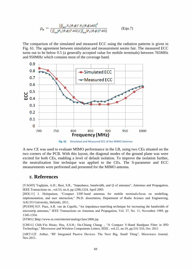
69
(Equ.7)
The comparison of the simulated and measured ECC using the radiation patterns is given in
Fig. 61. The agreement between simulation and measurement seems fair. The measured ECC
turns out to be below 0.5 (a generally accepted value for mobile terminals) between 765MHz
and 950MHz which contains most of the coverage band.
Fig. 61 Simulated and Measured ECC of the MIMO Antenna
A new CE was used to evaluate MIMO performance in the LB, using two CEs situated on the
two corners of the PCB. With this layout, the diagonal modes of the ground plane was were
excited for both CEs, enabling a level of default isolation. To improve the isolation further,
the neutralization line technique was applied to the CEs. The S-parameter and ECC
measurements were performed and presented for the MIMO antenna.
E. References
[YAG05] Yaghjian, A.D.; Best, S.R., “Impedance, bandwidth, and Q of antennas”, Antennas and Propagation,
IEEE Transactions on , vol.53, no.4, pp.1298,1324, April 2005
[HOL11] J. Holopainen, “Compact UHF-band antennas for mobile terminals:focus on modelling,
implementation, and user interaction,” Ph.D. dissertation, Department of Radio Science and Engineering,
AALTO University, Helsinki, 2011.
[PUE89] H.F. Pues, A.R. van de Capelle, “An impedance-matching technique for increasing the bandwidth of
microstrip antennas,” IEEE Transactions on Antennas and Propagation, Vol. 37, No. 11, November 1989, pp
1345-1354.
[STM12 ]http://www.st.com/internet/analog/class/1806.jsp
[CHI11] Chih-Yin Hsiao; Hsu, S.S.H.; Da-Chiang Chang; , "A Compact V-Band Bandpass Filter in IPD
Technology," Microwave and Wireless Components Letters, IEEE , vol.21, no.10, pp.531-533, Oct. 2011
[ART11]T. Arthur, “RF Integrated Passive Devices: The Next Big, Small Thing”, Microwave Journal,
Nov.2011.

70
[SHI11] S. Shim and S. Hong, "A CMOS Power Amplifier With Integrated-Passive-Device Spiral-Shaped
Directional Coupler for Mobile UHF RFID Reader", IEEE Transactions in Microwave Theory and Techniques,
Vol. 59, No. 11, pp. 2888-2897, November 2011.
[SAM13] F. Yang, R. Samii, “Microstrip antennas integrated with electromagnetic band-gap (EBG) structures: a
low mutual coupling design for array application”, Transactions on Antennas and Propagation, Vol. 51 Issue 10,
October 2003.
[CHI13] C.-Y. Chiu, X. Liu, F. Gao and Z. Ying, “Reduction of Envelope Correlation on Non-metallic and
Metallic Chassis Phones,” International Workshop on Antenna Technology 2013 (iWAT 2013), Karlsruhe,
Germany, March 2013.
[ZHA13] S. Zhang, A.A. Glazunov, Z. Ying, S. He, “Reduction of the Envelope Correlation Coefficient With
Improved Total Efficiency for Mobile LTE MIMO Antenna Arrays: Mutual Scattering Mode,” IEEE Trans. on
Antennas and Propagation, vol. 61, no. 6, pp.3280-3291, June 2013.

71
VIII. Millimeterwave modules and measurement technique
A last important part of my research was focused on millimeter wave system. This work was
mainly done in the frame of Diane Titz PhD, and different master studies (Syazatul Maryam
AZHAR, Aimeric Bisognin, Nguyen Hong Duc). Cyril Luxey was the main supervisor of
Diane Titz, and several academic and industrial scientists have contributed to this work. This
study was also realized in the frame of the CREMANT, Orange Company was involved in
this project through the contribution of Patrice Brachat and Frederic Devillers. ST
Microelectronics company is also closely associated to this work : Fréderic Gianesello et
Romain Pilard from STM Crolles, and Claire Laporte and Hilal Ezzeddine de STM Tours
were involved in many part of this study. Finally, several collaborations have been realized on
this topic.

72
A. Motivation
Because of emerging data consuming application as video, the demand for high data rate
communications is growing exponentially worldwide. The future introduction of 5G
communications will require several hundreds Mb/s data rate wireless communications. For
Wireless Local Area Networks (WLANs), IEEE 802.11.AC standards can offer peak rates of
867 Mb/s for handheld device. However, this is realized with 160MHz of bandwidth, and by
taking all existing channels. The existing norms and coding can be improved but the data rate
will still be limited by its carrier frequency, as actual wireless communications only exploit
the 300 MHz-6 GHz band for its long range communications.
Moving to higher frequencies where large bandwidth can be obtained and towards non-
licensed band is very promising. Millimeter-wave (Mmw) frequencies from 30 GHz to 300
GHz have been used for many years for military applications. With the recent advances in
circuit technologies and low-cost integration solutions, Mmw spectrum can now be targeted
for high volume market applications.
One specific band has occupied the worldwide research and industrial community for more
than 10 years now; it is the Industrial, Scientific and Medical (ISM) 60 GHz band. Following
the Shannon theorem, the channel capacity is directly proportional to the bandwidth. So, one
way to increase the data rate of a communication is to increase its bandwidth. This is possible
around 60 GHz where lies one of the largest worldwide unlicensed band allocated in history.
The bandwidth reaches 7 GHz from 57 to 64 GHz in the US, Canada, and Korea; from 59 to
66 GHz in Japan; and up to 9 GHz from 57 to 66 GHz in Europe, as shown in Fig. 62.
Another interesting feature of working at Mmw frequencies is the short wavelength. Many
topologies, impossible to implement at lower frequencies, become feasible. Among them,
traditional microwave board elements that use Transmission Lines (TL), as 90° couplers,
hybrids, Bulter matrix, etc… The compact size of the 60 GHz radio also permits multiple
antenna solutions at the user terminal that are more complicated at lower frequency.
Fig. 62 Figure I.6. Worldwide spectrum avaibility in the 60 GHz band, from the WiGig consortium.

73
B. Design of passive millimeter wave circuits
A first important part of this study was focused on the design of mmW passive hybrid
coupler. We focus our effort on the integration of broadband and miniature couplers at
millimeter-wave frequencies. Due to the decrease of the wavelength (λ = 5 mm), couplers
using quarter-wave length lines become feasible. These passives circuits are used in mixers,
amplifiers, vector modulators .Their implementation on Silicon substrates is then necessary.
They are also very useful in beamforming networks where electronically-steered antenna
arrays are used to overcome the inherent oxygen absorption at 60 GHz, in medium-range
communications. Among the best available solutions, reflection-type phase shifters [3] and
Butler matrices [4] are often employed. The necessary couplers must be reasonably small and
enough wideband to maintain good results.
We designed a new wideband miniature branchline coupler integrated at 60 GHz in a
BiCMOS9MW technology and IPD technology, both from ST Microelectronics. First, theory
and equations of the novel coupler are presented. As a proof-of-concept, a 2.2 GHz coupler is
designed on a duroid substrate and measured. Then, designs at 60 GHz in Silicon and IPD
technologies are described and compared to state-of-the art recently published couplers.
Finally, the integration of the IPD coupler in a low-cost Butler matrix is fully described.
1. Coupler design
a) Coupler Theory and Design
Branchline couplers are usually avoided when compacity is needed because of their large size.
However, compared to coupled-line and Lange couplers, their implementation is less
dependent on process variation and easier either on multi-level or single metallization
processes. To cover the 57-66 GHz band, wideband performance is necessary. The use of an
all-lumped component version is then usually excluded because of their narrowband
characteristics. Our coupler takes advantage of both microstrip lines and lumped capacitors as
an efficient mix to achieve a small footprint and a wide bandwidth.
As shown in Fig. 63, the proposed coupler is based on two cascaded Quasi-Lumped
Quadrature Couplers (QLQC). In addition, a short-circuited stub is used in the central
connection between the two couplers for matching purpose.
Za, La
Za, La
Za, La
Za, La
Zb, Lb
Zb, Lb
Zb, Lb
Zb, Lb
Zc, Lc
Zc, Lc
C1 C1C2 C2
1 2
3 4
A
A’
B B’
Fig. 63 Proposed Coupler Topology.

74
b) Duroid Implementation at 2.2 GHz
As a proof of concept, two couplers were realized on a 0.762-mm thick Duroid substrate (εr =
2.2, tan δ = 0.001) using Interdigitated (Int) capacitance and discrete capacitors. To comply
with our realization capability, the central frequency was set to 2.2 GHz. The quarter-
wavelength is equal to 2.3 cm which lead to an estimated overall footprint of 7.8 cm² for a
conventional branchline coupler. The realized couplers occupy an area of 6.0 cm² with the Int
capacitance, which gives a 23% size reduction and an area of 5.6 cm² with the discrete
capacitors (Fig. 64.a).
Fig. 64 Fabricated couplers at 2 GHz on PCB substrate. with interdigitated capacitance, (b) Simulated and measured reflection coefficient |S11| and isolation |S41| of the coupler.
The Interdigitated coupler was simulated using Momentum. The comparison between
simulation and measurement is presented in Fig. 64.b and Fig. 65. A quite good match is
obtained except a slight frequency shift of 4 %, mainly due to realization accuracy. We obtain
a measured -10 dB matching bandwidth of 36 % as expected from 1.89 GHz to 2.66 GHz
(Fig. 64.b), a ±1 dB amplitude imbalance, and a ±2° phase imbalance around 90° (Fig. 65.b)
of 28 % from 1.97 GHz to 2.57 GHz. These results show great promise for implementation at
higher frequencies.
-4
-2
0
2
4
1.50 1.75 2.00 2.25 2.50 2.75 3.00
Am
plit
ud
e Im
bal
ance
(d
B)
Frequency (GHz)
Measurement
Simulation
-120
-110
-100
-90
-80
-70
-60
1.50 1.75 2.00 2.25 2.50 2.75 3.00
Ph
ase
Imb
alan
ce (
°)
Frequency (GHz)
Measurement
Simulation
Fig. 65 Simulated and measured amplitude and phase imbalance of the coupler.

75
c) Silicon Integration and Design
The coupler was designed and fabricated in BiCMOS9MW technology (Fig. 66) because its
back-end of line (BEOL) has been optimized for millimeter-wave frequencies. In order to
minimize transmission losses, the microstrip lines are etched on the 3.88 µm-thick M6-Alucap
layers and its ground plane on the 1 µm-thick M1-M2 layers. It was simulated using HFSS for
full-wave simulations. MIM capacitors from the ST Microelectronics Design Kit were used.
The full 60 GHz band (57-66 GHz) is covered with a 0.5 dB amplitude imbalance and a 1°
phase imbalance at worst, for a 82% size reduction compared to classical branchline couplers
in the same technology (0.08 mm² instead of 0.44 mm²).
G
G
G
S
S
C1
C2 G
G
G
S
S
Fig. 66 Layout of the realized couplers in BiCMOS9MW.
Fig. 67 . De-embedded performance of the two realized couplers (thick lines) compared to HFSS simulation (crossed lines).
d) IPD Integration and Design
A promising way to think about the integration of the IC’s and the radiating element is the
antenna-in-package solution. In this integration scheme, the antenna is realized on a low-loss
substrate and can be directly implemented into the packaging. Lately, the tendency has been
going to PCB package because they are low-cost. The IC is flip-chipped on the PCB board

76
and the antenna and beamforming network are implemented at the RF level. The proposed
solution is to use the IPD technology from ST Microelectronics for the couplers and
associated low-loss passive circuits. Indeed, the IPD technology is low-loss when compared
to Silicon technology and allows scaling down passive components.
The signal lines of the realized coupler (Fig. 68) are etched on the 3-µm thick M3 layer and
its ground plane on the 6-µm thick M2 layer. They were simulated using HFSS. MIM
capacitors between layers M2 and M3 are used. Simulated results are summarized in Tab. 4.
We obtained the same performance than for the Silicon couplers with a 73% size reduction
(0.2 mm² instead of 0.73 mm²).
Fig. 68 Layout of the fabricated coupler in IPD
S11
S33
S41
S31
S21
Fig. 69 Simulated (solid lines) and measured (dashed lines) S-parameters, Amplitude Imbalance and Phase Imbalance of the DT coupler.
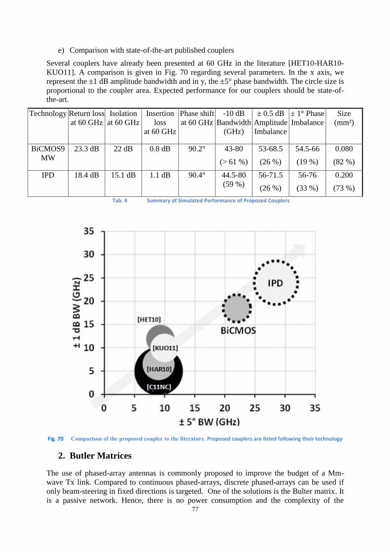
77
e) Comparison with state-of-the-art published couplers
Several couplers have already been presented at 60 GHz in the literature [HET10-HAR10-
KUO11]. A comparison is given in Fig. 70 regarding several parameters. In the x axis, we
represent the ±1 dB amplitude bandwidth and in y, the ±5° phase bandwidth. The circle size is
proportional to the coupler area. Expected performance for our couplers should be state-of-
the-art.
Technology Return loss
at 60 GHz
Isolation
at 60 GHz
Insertion
loss
at 60 GHz
Phase shift
at 60 GHz
-10 dB
Bandwidth
(GHz)
± 0.5 dB
Amplitude
Imbalance
± 1° Phase
Imbalance
Size
(mm²)
BiCMOS9
MW
23.3 dB 22 dB 0.8 dB 90.2° 43-80
(> 61 %)
53-68.5
(26 %)
54.5-66
(19 %)
0.080
(82 %)
IPD 18.4 dB 15.1 dB 1.1 dB 90.4° 44.5-80
(59 %)
56-71.5
(26 %)
56-76
(33 %)
0.200
(73 %)
Tab. 4 Summary of Simulated Performance of Proposed Couplers
Fig. 70 Comparison of the proposed coupler to the literature. Proposed couplers are listed following their technology
2. Butler Matrices
The use of phased-array antennas is commonly proposed to improve the budget of a Mm-
wave Tx link. Compared to continuous phased-arrays, discrete phased-arrays can be used if
only beam-steering in fixed directions is targeted. One of the solutions is the Bulter matrix. It
is a passive network. Hence, there is no power consumption and the complexity of the

78
transceiver architecture is relaxed. Compared to other solutions, namely the Rotman lens and
the Blass Matrix, the Butler matrix is chosen for its easier implementation.
As shown in Fig. 71, a 4x4 Butler matrix is made of four 90° couplers, two 45° phase shifters
and two crossovers [BUT61]. By selecting one of the inputs while the remaining are matched to
50 Ω, four different sets of phase differences are produced between the output ports of the
matrix. Usually, the selection of the input port is made by an SP4T switch. When the matrix is
followed by an antenna array, it then generates four different radiated beam angles pointing in
the ± 15° and ± 45° directions depending on the input port with the configuration presented in
Fig. 71. 8x8 matrices can also be designed. They generate eight different beams, but their
layout becomes more complicated and larger with an increase into the insertion loss.
Fig. 71 Schematic of a Butler matrix.
a) Design in IPD Process
The layout of the Butler matrix realized in IPD process is shown in Fig. 72. The IPD process
was chosen compared to an implementation on Silicon because its cost is lower and it enable
to fabricate the beamforming network and antennas on the same substrate. The simulations
were performed using the FEM solver, HFSS. These results were presented in [J14CP].
It uses the optimized 90° couplers presented in B.1.d to miniaturize its size while maintaining
good performance over the all bandwidth. Due to the good isolation of the coupler, the Bulter
matrix can operate without loading the unused ports, thus, without inserting any bulky and
lossy switch for port selection, not easy to design at this frequency.
When using microstrip lines and single layer technologies, crossovers are most of the time
made by cascading two 90° couplers [MOU10] which is a quite large solution, as presented in
previous section. Here, the proposed crossovers are achieved by crossing the lines on different
layers of the IPD Process using the multilayer feature [CHI10]. One of the line remains on
M3, while the other one is laid on M2 linked by two vias. For matching purpose, the line on
M2 is made wider. In our case, as the ground plane is set on M2, we etched away on purpose
around the crossover. Simulated results show amplitude and phase imbalances between the
two lines being respectively below 0.017 dB and 2.8° in the 60 GHz band.
An efficient 45° phase shifter can be designed with different techniques. In our design, we
choose to insert a simple delay line. Simulation results show amplitude and phase imbalances
between the microstrip lines being respectively below 0.14 dB and 10° in the whole 60 GHz
band. The overall footprint of the Butler matrix, pads not included, is 1.6 x 1 mm².

79
G
G
G
S
S
G
G
G
S
S
50 Ω
G
G
G
S
S
G
G
S
S
90° Coupler
Crossover
45° Phase Shifter
Stub
CMIM
1.6 mm
1 mm
Port 5
Port 6
Port 1
Port 2
Fig. 72 Layout of the fabricated Butler matrix. Ports 3, 4, 7 and 8 are matched to 50 Ω.
b) Realization and Results
The measurement of the matrix was performed in STMicroelectronics, Crolles using on-wafer
probing and a setup composed of two GSGSG Infinity probes and a 67 GHz VNA. Since this
passive network is symmetrical, only two input ports (Port 1 and 2) and two output ports will
be fed using GSGSG probes. In the first configuration, the output GSGSG pads are connected
to ports 5 and 6 (Fig. 72) and in the second one, to ports 7 and 8. The others input ports (Port
3 and 4) are always matched to 50 Ω. For the 50 Ω load, we used resistors from the low
frequency STMicroelectronics DK.
Fig. 73 Picture of realized Butler matrix
The measured and simulated results for the two configurations are presented in Fig. 74. First,
the insertion loss (IL) and phase difference (Phase Diff) from Port 1 to Port 5, 6, 7, and 8 are
presented, and then for Port 2. The IL is lower than 11 dB at 60 GHz and on the whole 57-66

80
GHz BW. If we take into account the inherent loss of hybrid couplers (6 dB since two
couplers are used per path), then we achieve IL lower than 5 dB. As the couplers, presented in
previous section, achieve approximately 1.5 dB IL on the BW, we can deduce than 2 dB IL
come from the crossovers and 45° phase shifters. Another reason to explain the value of these
losses can be found into the implementation of the 50 Ω resistors. We used elements from the
low frequency STMicroelectronics DK. We suspect these resistances to be different from 50
Ω value. Fig. 75 shows another representation of the measured and simulated results using the
Smith chart. For a better visibility, the frequency is only plot between 58 to 62 GHz on the
Smith chart. The closer we are from the center of the chart, the higher the losses. A good
amplitude imbalance is obtained if all the plotted S-parameters are on the same circle. This is
almost true when port 2 is fed. It can be seen on Fig. 75 that when fed through Port 1, the
signal has a delay around 45° between the adjacent ports, while when fed through Port 2, the
delay is close to 135°. A maximum phase error of 13.6° at 60 GHz is measured. The reflection
coefficient is lower than -10 dB over the 57-66 GHz band for all ports and the isolation higher
than 15 dB.
45 50 55 60 6540 70
-20
-15
-10
-5
-25
0
Frequency (GHz)
IL (
Port
1)
45 50 55 60 6540 70
-20
-15
-10
-5
-25
0
Frequency (GHz)
IL (
Port
2)
45 50 55 60 6540 70
-315-270-225-180-135
-90-45
-360
0
Frequency (GHz)
Phase D
iff
(Port
2)
45 50 55 60 6540 70
-315-270-225-180-135-90-45
-360
0
Frequency (GHz)
Phase D
iff
(Port
1)
S71
S81
S51S61 S62
S52
S72
S82
Δφ(S62)-Δφ(S52)
Δφ(S82)-Δφ(S72)
Δφ(S72)-Δφ(S62)
Δφ(S61)-Δφ(S51)
Δφ(S71)-Δφ(S61)Δφ(S81)-Δφ(S71)
Fig. 74 Simulated (solid lines) and measured (dotted lines) insertion loss and phase difference for Port 1 and 2.
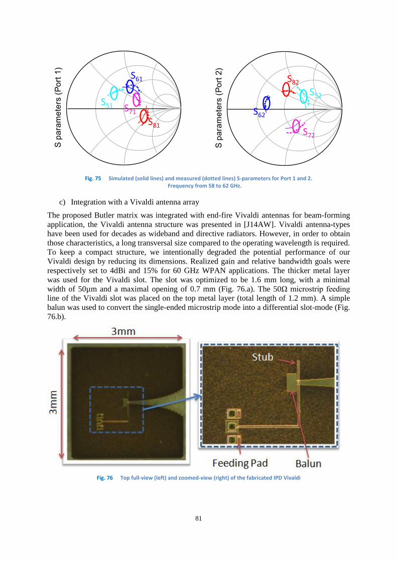
81
freq (58.00GHz to 62.00GHz)
S p
ara
me
ters
(P
ort
1)
freq (58.00GHz to 62.00GHz)
S p
ara
me
ters
(P
ort
2)
S81
S61
S51 S71
S82
S62
S52
S72
Fig. 75 Simulated (solid lines) and measured (dotted lines) S-parameters for Port 1 and 2. Frequency from 58 to 62 GHz.
c) Integration with a Vivaldi antenna array
The proposed Butler matrix was integrated with end-fire Vivaldi antennas for beam-forming
application, the Vivaldi antenna structure was presented in [J14AW]. Vivaldi antenna-types
have been used for decades as wideband and directive radiators. However, in order to obtain
those characteristics, a long transversal size compared to the operating wavelength is required.
To keep a compact structure, we intentionally degraded the potential performance of our
Vivaldi design by reducing its dimensions. Realized gain and relative bandwidth goals were
respectively set to 4dBi and 15% for 60 GHz WPAN applications. The thicker metal layer
was used for the Vivaldi slot. The slot was optimized to be 1.6 mm long, with a minimal
width of 50µm and a maximal opening of 0.7 mm (Fig. 76.a). The 50Ω microstrip feeding
line of the Vivaldi slot was placed on the top metal layer (total length of 1.2 mm). A simple
balun was used to convert the single-ended microstrip mode into a differential slot-mode (Fig.
76.b).
Fig. 76 Top full-view (left) and zoomed-view (right) of the fabricated IPD Vivaldi

82
Based on this Vivaldi type radiating element, a 4 element linear antenna array was designed
as shown in Fig. 77. The distance between the 4 antennas is equal to a halfwavelength
(2.5mm). The antenna array was connected to the 4x4 bulter matrix presented previously.
The antenna array was measured on the mmW set-up for two different configurations: when
the port 1 is fed (Fig. 78.a) and when the port 2 is fed (Fig. 78.b). A maximum gain of 7.32
dB is obtained with a beam tilt of 22.5° as expected.
Fig. 77 Pitcure of the antenna array prototype and probe-fed measurement of the structure
Fig. 78 3D radiation pattern measurement for Port 1(a) and Port 2 (b) fed

83
C. Antenna in Package design for millimeter waves
Concurrently to the design of mmW circuit, we have also studied to best solution for the
antenna system. Two antenna main solutions have emerged at 60 GHz. The first one is the
Antenna-on-chip (AoC) technology where the antenna is directly integrated with the front-end
circuit on the same substrate. This solution has become affordable at millimeter wave
frequencies thanks to the short wavelength (λ0 = 5mm) and high permittivity of the RF front-
end substrates, usually in silicon technology (εr = 11.9). The entire realization of the antenna
and circuits on the same die helps in reducing the manufacturing costs and simplifying the
front-end/antenna interconnection. The second technique is the Antenna-in-Package (AiP)
solution. The antenna is fabricated on a separate substrate and/or package which will enclose
the RF chip. At millimeter wave frequencies, the RF die has to be placed as close as possible
to the antenna solution to avoid huge losses. This is the most employed low-frequency
solution as the antennas can be realized on a cheaper and low-loss substrate. High gain and
high total efficiency are easy to achieve for the antenna element at the expense of higher
complexity and losses in the interconnections with the front-end module compared with the
AoC solution.
The AiP solution seems to be the most promising antenna solution to highly integrate Mmw
radios for high-speed short-range wireless communications because of high gain and broad
bandwidth. Low-loss and low-cost substrates can be used at the expense of more complicated
antenna to RF chip interconnections.
Materials and process technologies capable of realizing AiP solutions in high volume while
respecting the above criteria are limited. Among them, we can cite HR silicon, Teflon,
ceramics, and polymers. In recent years, an increase interest has been focused on low and
high temperature cofired ceramic (LTCC and HTCC) and organic materials.
1. Designs with IPD Process
The IPD™ process developed by ST Microelectronics Tours has been especially created for
lossless and miniature passive devices like resistors, capacitors or inductors at low
frequencies. It has already been used previously to implement couplers and a Butler matrix. A
simplified side view of the most significant layers of this process is presented in Fig. 79 (a).
On top of the glass substrate (εr=4.6), we choose to use the third level of metallization
(Meta3, h=3 µm) which is covered by a BCB material (εr=2.7) to etch the patch antenna. In
an AiP perspective, an organic package could benefit from the IPD technology to widen the
antenna bandwidth but it will be more expensive. The IPD superstrate is flip-chipped on the
organic package. Two bump sizes are available, 140 µm and 240 µm, respectively called
micro and macro bumps. The general SiP strategies developed in Fig. 79.a would then
become the one presented in Fig. 79.b and c. In both configurations, thanks to the use of the
IPD no cavity could be needed in the organic package.
PCB
RFIC IPD
(b)
PCB
RFIC
IPD
(c)
Glassεr=4.6
tan δ=0.001h = 400 µm
BCB
εr=2.7 /tanδ=0.0009 h = 13.5 µm
Meta3h = 3 µm
(a)
Fig. 79 (a) IPD process build-up. (b) Top die attach and (c) bottom die attach strategies using IPD.

84
a) Antenna design
Several size of bumps have been used during this study, I will here present the last antenna
version using macro-bumps. These results have been presented in [C12EU]. A direct coupling
from a microstrip line etched on the Taclamplus substrate is used to feed the patch fabricated
on the IPD™ substrate. As before, the microstrip is fed using GSG pads and incorporates a
double-tuning stub. This part is still etched on the Taclamplus material. Then, above the line,
we electromagnetically couple the IPD™ patch. The IPD™ substrate is flip-chipped and
soldered onto the Taclamplus using micro-bumps. After assembly, the air height between the
IPD™ and the Taclamplus is given to be around 90μm with a ±10 um tolerance. The HFSS
model and its coordinate system, as well as the realized antenna are presented in Fig. 80.a.
Fig. 80 (a) HFSS model of the coupled IPD patch antenna with macro-bumps. (b) Picture of the realized coupled IPD patch antenna.
After assembly, the air height between the IPD™ and the Taclamplus is given to be around
160 μm with a ±10 um tolerance. These results have been presented in [C12LA].
Simulated and measured reflection coefficients are presented in Fig. 81. The agreement is
very good with a measured S11 below -10 dB from 55 to 64.2 GHz. However, we obtain a
frequency shift of 1 %. We can see in Fig. 81.b that a variation of ±10 um can cause this kind
of frequency shift. Using macro-bumps, we have gained more the 4 GHz of bandwidth.
Fig. 82.a presents the realized gains in the broadside direction (ϕ,θ) = (0°,90°) which is the
direction of maximum radiation. Co-polarization and total realized gains are superposed as the
antenna is LP. The total realized gain is higher than 6 dBi from 53 to 66 GHz with a cross-
polarization level lower than -10 dBi. The simulated and measured radiation patterns are
plotted in the two main planes (E and H) at 60 GHz (Fig. 82). We obtain a maximum
measured realized gain of 9.31 dBi at Phi=28° and Theta=90° in the E-plane and a measured
realized gain of 7.87 dBi in the broadside direction (ϕ,θ) = (0°,90°) very close to the simulated
result (7.88 dBi). Simulated radiation efficiency is equal to 96 % at 60 GHz.Fig. 83.b presents
the measured and simulated 3D patterns. We obtain a very good agreement. If we use the
proposed method in Chapter III to compute the efficiency, we find that 83.3% of the radiation
efficiency is due to the 74% measured pattern and 12% due to the 26 % simulated pattern.
This gives us a radiation efficiency equal to 95.3%, very close to the 96% expected.
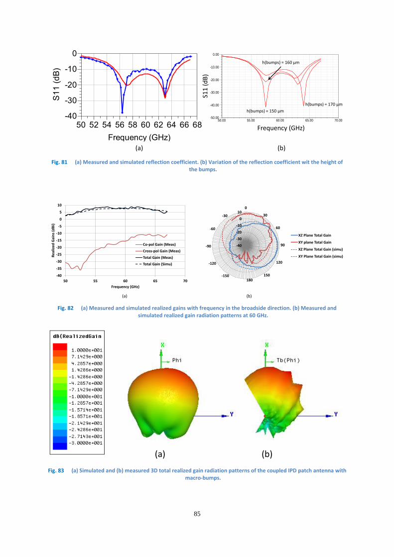
85
52 54 56 58 60 62 64 6650 68
-30
-20
-10
-40
0
Frequency (GHz)
S1
1 (
dB
)
50.00 55.00 60.00 65.00 70.00Freq [GHz]
-50.00
-40.00
-30.00
-20.00
-10.00
0.00
Y1
v13_patch_GSG_bump_heightS11 ANSOFT
Imported
Setup1 : Sw eepbump_height='0.15mm'
Setup1 : Sw eepbump_height='0.17mm'
Frequency (GHz)
S11
(d
B)
(a) (b)
h(bumps) = 170 µm
h(bumps) = 150 µm
h(bumps) = 160 µm
Fig. 81 (a) Measured and simulated reflection coefficient. (b) Variation of the reflection coefficient wit the height of the bumps.
-40
-35
-30
-25
-20
-15
-10
-5
0
5
10
50 55 60 65 70
Re
aliz
ed
Gai
ns
(dB
i)
Frequency (GHz)
Co-pol Gain (Meas)
Cross-pol Gain (Meas)
Total Gain (Meas)
Total Gain (Simu)
-40
-30
-20
-10
0
100
30
60
90
120
150180
-150
-120
-90
-60
-30
XZ Plane Total Gain
XY plane Total Gain
XZ Plane Total Gain (simu)
XY Plane Total Gain (simu)
(a) (b)
Fig. 82 (a) Measured and simulated realized gains with frequency in the broadside direction. (b) Measured and simulated realized gain radiation patterns at 60 GHz.
(a) (b)
Fig. 83 (a) Simulated and (b) measured 3D total realized gain radiation patterns of the coupled IPD patch antenna with macro-bumps.
86
2. Designs on Organic Package
Within our collaboration with STMicroelectronics, we have been able to start the design of
several antennas on their organic stack-up. This led us to work together with the Berkeley
Wireless Research Center (BWRC). The aim of this project is to achieve I/Q spatial
combining, the I and Q signals at the output of a transmitter are not combined on chip
anymore, but spatially thanks to two different antenna arrays.
The objectives of this part are to design two linear antenna arrays on the organic package in a
limited size while achieving same characteristics and especially for each element of each
array. The return loss of each antenna has to be below 10 dB from 57 to 66 GHz, the gain of
each element above 5 dBi on the same band, with a ±30° aperture at least. The chosen
topology is an aperture coupled antenna. The antenna is fed on the top part of the package and
radiates through the bottom part. Hence, the IC on the top of the package won’t be disturbed
by the antenna radiation.
Fig. 84 presents the top, bottom and side view of the package. On the top, the IC will be flip-
chipped to the package using bumps and a 250-µm pitch. On Fig. 84, only the feed lines to the
antennas are represented but this metallization will also be used for other RF, DC feeds and
SMD components if necessary. We can see the slots on the second metallization on the top
view of the aperture coupled antennas and the patches on the bottom view. All around each I
and Q arrays there is a metalized ring, from the ground plane to the bottom metal layer. This
ring is here to avoid substrate and surface modes. It is represented as a metal wall in
simulation, but will be made of vias in the practical realization. Both simulations showed that
we can model these vias by a wall with good approximation of the behavior of the vias,
leading to faster simulations. The package dimensions are 12 x12 mm. Because the IC has its
I and Q outputs on two opposite sides of the chip, the arrays have been put symmetrically on
two opposites sides of the package. The two arrays could not be put closer because of the IC
and the necessary space for the feed lines. The elements of each array are put at λ0/2 (2.5 mm)
from each other and the two arrays at 1.5 λ0 from each other.
Top view
IC
Bottom view
I arrayQ array
Side view
Bumps
2.5 mm
12 mm
Fig. 84 Organic package design.
A prototype was realized and a picture is presented on Fig. 85. Antenna elements are
measured one by one as the global array can only be fed from the chip. |S11| measurements,
achieved with a microelectronic probe from our measurement set-up are presented in Fig. 86.

87
Fig. 85 Fabricated HDI module. Top (left) and bottom (right) views.
Fig. 86 |S11| measurement of various patches of the fabricated array.
Co-polarized realized gain measurements are compared to simulations in Fig. 87.a. Simulated
and measured 3D radiation pattern is presented in Fig. 87.b. Co-polarized realized gain
measurement in the H plane for patch 1 is presented in Fig. 88. Overall behavior is quite
similar. However, lower measured gain is obtained. This can be due to the fact that as we
measure one antenna only, the other ones are left open (and not matched to 50Ω as this is
done in simulation). The measurements were done on several samples showing a good
reproducibility.
Fig. 87 (a) Realized gain measurement versus frequency, (b) 3D co-polarized realized gain measurement for patch 1.

88
Fig. 88 Co-polarized realized gain measurement in the H plane for patch 1.
To conclude this part, based on the collaboration with Berkeley Wireless Research Center, a
complete system was assembled and tested. A measurement with the BWRC chip was
realized and presented in [C13JS]. The organic prototype was not available to meet the ISSCC
deadline, and a specific design made on Rogers material was done for this purpose and is
presented in Fig. 89.a. Main results for the Other the Air measurements (realized by BWRC)
are presented in Fig. 89.b. A maximum data rate of 6Gb/s is obtained for a 16-QAM
modulation with a power amplifier average efficiency of 16.5%.
Fig. 89 (a) Picture of the protype (b) Measured QPSK and 16PSK constellation (c) Demo parameters

89
D. MillimeterWave system caracterization
The main catalist of the different innovation in the millimeterwave domain was the
development of an innovative set-up for mmW antenna characterisation. This system was first
designed by Sylvain Ranvier during his PhD, and improved during the Diane Titz PhD.
At 60 GHz, the antenna can be on-chip but more recently, the millimeter community is
moving to integration into a different substrate. Based on these two integration schemes, two
different ways to characterize their radiation performance have arisen.
The integration of the antenna into a low loss substrate which is different from the Integrated
Circuit substrate is the best solution at low frequency and those antennas are connector-fed to
be measured in large anechoic chambers. A logical approach could have been to reproduce
this characterization scheme at 60GHz. However, it was shown in [RAN09] that the
connector, being as big as (or even bigger than) the antenna itself, is strongly disturbing the
accuracy of the recorded radiation pattern. As a small improvement, it was demonstrated
possible in [LAM10] to obtain acceptable results if placing some absorber sheets over the
connector. However, another issue is the de-embedding of the connector from the
measurement as it won’t physically exist in the final design. Indeed the soldering stage can
modify or deteriorate the small antenna before the measurement. Another important point is
the big size of an anechoic chamber at lower frequency which is not compatible with a mmW
frequency transmission characterization of medium gain antenna (<10 dBi) as the free-space
attenuation of the electromagnetic waves is quite large and it would require high level power
sources which is expensive and difficult to achieve. Finally, the connector-fed approach is not
compatible with the Antenna-on-Chip (AoC) technology where the antenna is closely
integrated within the RF front-end module.
We believe the other way to handle an accurate characterization setup is to think how to
measure an Antenna-on-Chip. As the microelectronic Radio-Frequency (RF) circuits are
closely integrated within the antenna, a logical approach is to derive a probe measurement
procedure. However, several drawbacks exist. The close environment of a probe tester is
usually all metallic, composed of a chuck base, a microscope, the probes and the positioners.
The first measurements made in this way proved that the radiation pattern was completely
disturbed [LAN10]. A first step is to get rid of the metallic chuck as was done in [PIL09],
[ZWI04]. Also, the AUT has to be horizontally maintained very accurately to ensure a stable
and solid contact between the microelectronic probe and the antenna pads which is important
for characterization accuracy and also to avoid damaging the expensive probe. In [PIL09], the
metallic chuck was replaced by a rexolite chuck as a first interesting enhancement. In
[ZWI04], no chuck is anymore used and the antenna is maintained by two substrate pieces of
FR4 (Flame Resistant 4). A better solution would be to use a material with a lower
permittivity and possibly close to one. Hence, the radiation pattern of the antenna would not
be disturbed at all by the holding pieces: metal-free for the chuck or holder. Then we decide
to develop a solution based on a special holder made of foam. Thus, the radiation pattern
below the antenna (if the antenna is fed by the probe on its top face) can be recorded and the
foam won’t disturb the measure at all. Then, another issue is the probe itself. A study has to
be made concerning its influence on the radiation pattern and especially how to extract the
exact losses introduced by the probe itself only. Considering the two aforementioned options,
we tried to keep the best from both, and we concurrently developed a setup quite similar to
the one described [BEE10].

90
1. Description of the Setup
This principle of the setup was first described in [RAN09]. A picture of the latest
configuration of the measurement setup is shown in Fig. 90.
Fig. 90 Pictures of the measurement setup (Global view and closer view).
a) RF Parts
Several configurations have been used on this set-up and I will present the configuration
based on a 60GHz VNA.
A schematic view of the setup is presented in Fig. 91. A signal is generated by the Agilent
Vector Network Analyzer (VNA) E8361A. To control the power level of this signal and for
calibration purpose, an Agilent E4418B power meter connected through a 10dB coupler is
used after this amplification. The output power is about a 0-dBm at 60 GHz. An Agilent
V281A Mmw-to-coax adapter allows conveying this signal to the microelectronic probe
through a specific 60 GHz semi-rigid cable. A Ground Signal Ground (GSG) microelectronic
probe feeds the Antenna Under Test (AUT).
At the receiver side, an HP 11970V harmonic mixer is directly connected to a Flann 25240-20
horn antenna to down-convert the received 60 GHz signal. This direct attachment is indeed
really important because the Local Oscillator (LO) and Intermediate Frequency (IF) low
frequency signals, at respectively 4.3 GHz and 310 MHz, can be conveyed with low-cost
flexible coaxial cables allowing the mechanical parts of the setup freely moving during the
measurement slot. This option especially helps to record the received signal with a better
accuracy. The power level of the LO signal is then monitored with an HP 8563E spectrum
analyzer or directly with the Agilent Vector Network Analyzer (VNA) E8361A. The VNA
and spectrum analyzer are controlled from a computer via a General Purpose Interface Bus
(GPIB) bus and a custom-made Labview code.
The Agilent Vector Network Analyzer (VNA) E8361A enables the S11 measurement of the
AUT.
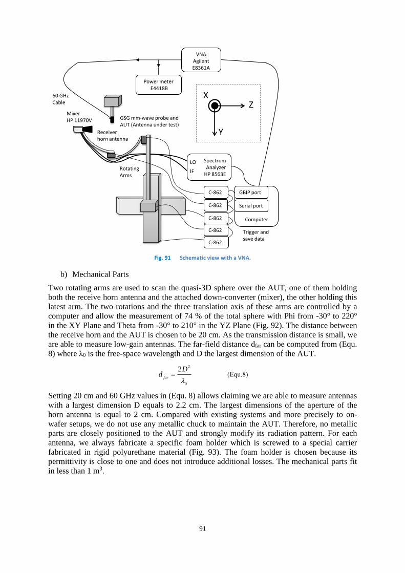
91
Rotating Arms
Trigger and save data
60 GHz Cable
GSG mm-wave probe andAUT (Antenna under test)
Mixer HP 11970V
Spectrum Analyzer
HP 8563E
Computer
GBIP port
Serial port
C-862
Receiverhorn antenna
C-862
C-862
C-862
C-862
IF
LO
VNAAgilentE8361A
Power meterE4418B
Y
ZX
Fig. 91 Schematic view with a VNA.
b) Mechanical Parts
Two rotating arms are used to scan the quasi-3D sphere over the AUT, one of them holding
both the receive horn antenna and the attached down-converter (mixer), the other holding this
latest arm. The two rotations and the three translation axis of these arms are controlled by a
computer and allow the measurement of 74 % of the total sphere with Phi from -30° to 220°
in the XY Plane and Theta from -30° to 210° in the YZ Plane (Fig. 92). The distance between
the receive horn and the AUT is chosen to be 20 cm. As the transmission distance is small, we
are able to measure low-gain antennas. The far-field distance dfar can be computed from (Equ.
8) where λ0 is the free-space wavelength and D the largest dimension of the AUT.
2
0
2far
Dd
(Equ.8)
Setting 20 cm and 60 GHz values in (Equ. 8) allows claiming we are able to measure antennas
with a largest dimension D equals to 2.2 cm. The largest dimensions of the aperture of the
horn antenna is equal to 2 cm. Compared with existing systems and more precisely to on-
wafer setups, we do not use any metallic chuck to maintain the AUT. Therefore, no metallic
parts are closely positioned to the AUT and strongly modify its radiation pattern. For each
antenna, we always fabricate a specific foam holder which is screwed to a special carrier
fabricated in rigid polyurethane material (Fig. 93). The foam holder is chosen because its
permittivity is close to one and does not introduce additional losses. The mechanical parts fit
in less than 1 m3.

92
Y
Z
Probe
θ
AUT
Side view Top view
Y
X
Probe
ϕ
AUT
Front view
Z
X
ϕ
AUT
Probe
Fig. 92 Measurable part of the sphere in the XY, XZ, and YZ planes.
Fig. 93 RF probe and foam holder
2. Calibration
a) Mechanical Calibration
Several mechanical steps must be performed before starting the RF calibration. First, the AUT
has to be positioned on its holder and the holder has to be screwed on the carrier. To maintain
the AUT a cavity is made into the foam holder whose dimensions are those of the antenna
(Fig. 94.a). Then, two laser pointers, which can fit into the center of the rotating arms, are
used to accurately position the AUT at the center of the measurement sphere using the x, y,
and z translation motors (Fig. 94.b). Because the overall assembly of the two arms with the
mixer and the horn antenna is a bit heavy (1 kg), a slight inflexion of the two arms is observed
(<2°). However, we truly checked that no vibrations were happening during the measurements
mainly because the two arms were designed in reinforced but lightweight aluminum. To avoid
any electromagnetic reflections and diffractions, these two aluminum arms are covered by
thin-sheet absorbers. Then, a movable microscope is necessary to place the probe in-situ.

93
Cavity
Laser pointers
(a) (b)
Fig. 94 AUT in its foam holder maintain into a cavity. (b) Laser pointer for accurate positionning of the AUT.
b) RF Calibration Methodology
The calibration and the associated accuracy of such a setup are not trivial. In classic anechoic
chambers, the RF calibration is usually achieved with two reference antennas, having a known
realized gain. Designing a reference integrated antenna at these frequencies is quite
challenging. Reference antennas as horn antennas are often fed by a waveguide. By doing so,
the probe is not taken into account in the calibration procedure and the transmitted horn
antenna should be at the exact place of the AUT which would be quite complicated and a long
procedure in our case. So, we decided to implement a different sort of calibration.
We directly connect the 60-GHz cable to the receiving mixer using a waveguide-to-coax
adapter instead of connecting this cable to the AUT via a probe (Fig. 95). The 20-dB coupler
is useful to monitor the output power of the VNA. With 12.5 dB lost in the cable and 0.5 dB
lost in the adapters, the mixer experiences an input power close to -13 dBm, which is 10dB
lower than its 1-dB compression point (-3 dBm). The schematic with VNA is given in Fig. 95.
VNA-20 dB Coupler
Power SensorAgilentV8486A
Power MeterAgilentE4418B
Waveguide-to-Coax Adapter
Waveguide-to-Coax Adapter
MixerSpectrum Analyser LO
IF
Pr
60 GHz cable
Pm
Fig. 95 Schematic of the calibration procedure with the VNA.
This calibration is done for each polarization direction because we are forced to slightly twist
the two cables and add two short cables when we turn the receiving horn in order to measure
the cross-polarization level. Both calibrations are generally really close to each other. The
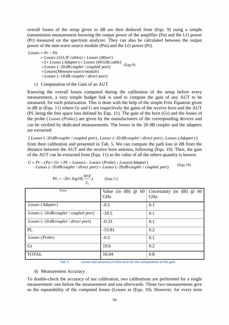
94
overall losses of the setup given in dB are then deduced from (Equ. 9) using a simple
transmission measurement knowing the output power of the amplifier (Pa) and the LO power
(Pr) measured on the spectrum analyzer. They can also be calculated between the output
power of the mm-wave source module (Pm) and the LO power (Pr).
( , ) ( ) 2 ( ) (60 )
( 20 / )( ) ( 10 / )
Losses Pr PaLosses LO IF cables Losses Mixer
Losses Adapter Losses GHz cableLosses dB coupler coupled portLosses Mmwave source moduleLosses dB coupler direct port
(Equ.9)
c) Computation of the Gain of an AUT
Knowing the overall losses computed during the calibration of the setup before every
measurement, a very simple budget link is used to compute the gain of any AUT to be
measured, for each polarization. This is done with the help of the simple Friis Equation given
in dB in (Equ. 11) where Gr and G are respectively the gains of the receive horn and the AUT
(PL being the free space loss defined by Equ. 11). The gain of the horn (Gr) and the losses of
the probe ( ( )Losses Probe ) are given by the manufacturers of the corresponding devices and
can be verified by dedicated measurements. The losses in the 20 dB coupler and the adapters
are extracted:
( ( 20 / )Losses dB coupler coupled port , ( 20 / )Losses dB coupler direct port , ( )Losses Adapter )
from their calibration and presented in Tab. 5. We can compute the path loss in dB from the
distance between the AUT and the receive horn antenna, following (Equ. 10). Then, the gain
of the AUT can be extracted from (Equ. 11) as the value of all the others quantity is known.
( ) ( ) ( ) ( 20 / ) ( 20 / )
G Pr Pa Gr PL Losses Losses Probe Losses AdapterLosses dB coupler direct port Losses dBcoupler coupled port
(Equ.10)
0
420 10( )
dPL log
(Equ.11)
TERM Value (in dB) @ 60
GHz
Uncertainty (in dB) @ 60
GHz
( )Losses Adapter -0.5 0.1
( 20 / )Losses dB coupler coupled port -19.5 0.1
( 20 / )Losses dB coupler direct port -0.33 0.1
PL -53.81 0.2
( )Losses Probe -0.5 0.1
Gr 19.6 0.2
TOTAL 16.04 0.8
Tab. 5 Losses and accuracy of each term for the computation of the gain.
d) Measurement Accuracy
To double-check the accuracy of our calibration, two calibrations are performed for a single
measurement: one before the measurement and one afterwards. Those two measurements give
us the repeatability of the computed losses (Losses in (Equ. 10). However, for every term
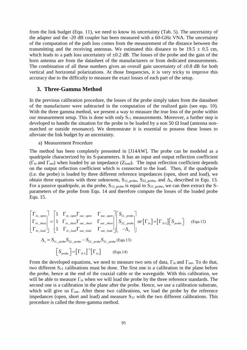
95
from the link budget (Equ. 11), we need to know its uncertainty (Tab. 5). The uncertainty of
the adapter and the -20 dB coupler has been measured with a 60-GHz VNA. The uncertainty
of the computation of the path loss comes from the measurement of the distance between the
transmitting and the receiving antennas. We estimated this distance to be 19.5 ± 0.5 cm,
which leads to a path loss uncertainty of ±0.2 dB. The losses of the probe and the gain of the
horn antenna are from the datasheet of the manufacturers or from dedicated measurements.
The combination of all these numbers gives an overall gain uncertainty of ±0.8 dB for both
vertical and horizontal polarizations. At those frequencies, it is very tricky to improve this
accuracy due to the difficulty to measure the exact losses of each part of the setup.
3. Three-Gamma Method
In the previous calibration procedure, the losses of the probe simply taken from the datasheet
of the manufacturer were subtracted in the computation of the realized gain (see equ. 10).
With the three gamma method, we present a way to measure the true loss of the probe within
our measurement setup. This is done with only S11 measurements. Moreover, a further step is
developed to handle the situation for the probe to be loaded by a non 50 Ω load (antenna non-
matched or outside resonance). We demonstrate it is essential to possess these losses to
alleviate the link budget by an uncertainty.
a) Measurement Procedure
The method has been completely presented in [J14AW]. The probe can be modeled as a
quadripole characterized by its S-parameters. It has an input and output reflection coefficient
(Γin and Γout) when loaded by an impedance (Zload). The input reflection coefficient depends
on the output reflection coefficient which is connected to the load. Then, if the quadripole
(i.e. the probe) is loaded by three different reference impedances (open, short and load), we
obtain three equations with three unknowns, S11_probe, S22_probe, and Δs, described in Equ. 13.
For a passive quadripole, as the probe, S12_probe is equal to S21_probe, we can then extract the S-
parameters of the probe from Equ. 14 and therefore compute the losses of the loaded probe
Equ. 15.
_ _ _ _ 11_
_ _ _ _ 22_ 3 3
_ _ _ _
1
1
1
in open in open out open out open probe
in short in short out short out short probe in probe
in load in load out load out load s
S
S or S
(Equ.12)
11_ 22_ 12_ 21_s probe probe probe probeS S S S (Equ.13)
1
3 3probe inS
(Equ.14)
From the developed equations, we need to measure two sets of data, Γin and Γout. To do that,
two different S11 calibrations must be done. The first one is a calibration in the plane before
the probe, hence at the end of the coaxial cable or the waveguide. With this calibration, we
will be able to measure Γin when we will load the probe by the three reference standards. The
second one is a calibration in the plane after the probe. Hence, we use a calibration substrate,
which will give us Γout. After these two calibrations, we load the probe by the reference
impedances (open, short and load) and measure S11 with the two different calibrations. This
procedure is called the three-gamma method.

96
4. Circular Polarization
Circularly Polarized (CP) antennas are very interesting when placed at one side of a radio
link, when the orientation of the two communicating devices is not known in advance. We
have presented the first measurement of probe-fed CP antennas including the axial ratio (AR)
in one direction, in 2D planes and in 3D.
a) Typical Ways to Measure a CP Antenna
To completely characterize the polarization of an antenna, it is necessary to determine the
polarization ellipse (Axial Ratio and Tilt Angle) and the sense of rotation of the electric field
vector. From the IEEE Standard Test Procedures for Antennas [IEE79], we can count four
different methods that may be employed to measure polarization: polarization-pattern method,
rotating-source method, multiple-amplitude-component method and phase-amplitude method.
In the polarization-pattern method, the linear receive antenna is rotated until the received gain
is at its maximum, the tilt angle of the horn antenna is then measured, then the AR and tilt
angle can be measured but not the sense of rotation. A disadvantage is that the probe antenna
shall be rotated 360° which is not convenient when the AR has to be measure for several
positions.
In the rotating-source method, the Linearly Polarized (LP) source antenna is still rotated, but
the direction of observation is changed at the same time. But, the rotation of the source
antenna should be much greater than its movement. The pattern is plotted at the same time as
the AR, but nor the tilt angle neither the sense of rotation can be measured.
In the multiple-amplitude-component method, all the polarization characteristics can be
determined. Four different antennas having different polarizations (vertical or horizontal LP,
45° or 135° LP, right-hand or left-hand CP) with known gains are used to measure the
response of the AUT. Using all six antennas is even more accurate. A modified version
involving only LP antennas can be employed to determine the AR and tilt angle provided that
the sense in not required. This method is the one that will be implemented. It will be more
detailed in b).
In the phase-amplitude method, all the data required for complete polarization determination
can be measured simultaneously. But, it needs a measurement set-up with phase capability
which is quite expensive and difficult to implement with satisfactory accuracy at 60 GHz.
b) Measurement of CP Antennas
In our measurement setup, the method I developed uses the modified version of the multiple-
amplitude-component method. We are then able to measure the AR and tilt angle by rotating
the LP receive horn antenna at 0° (horizontal), 45°, 90° (vertical), and 135° (-45°), for a fast
four point measurement. For that purpose, a motor could be used to rotate the horn and record
many points but because of weight issues in our setup, we decided to design a special horn
holder with four possible angle positions. The four positions of the horn antenna are shown in
Tab. 6. Measuring LP antennas, only 0° and 90° positions are required, but at least a third
position (45° or -45°) is mandatory to be able to compute the polarization ellipse as shown in
Fig. 96. This method was published in [J12AM].
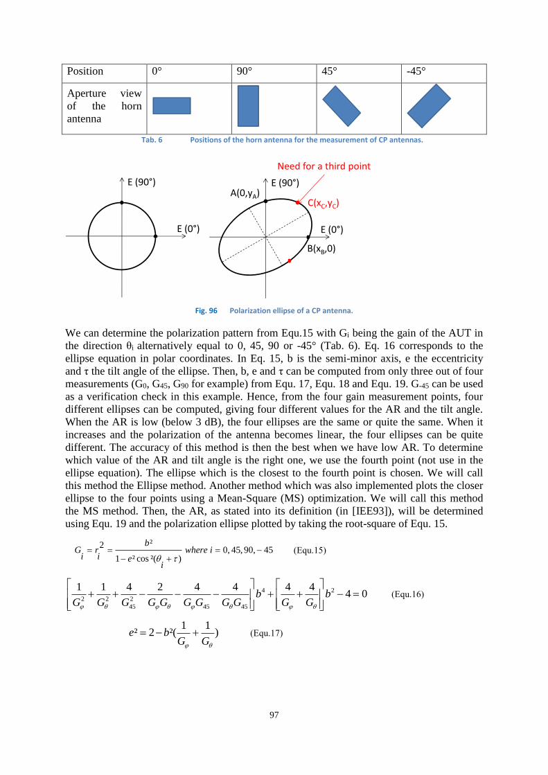
97
Position 0° 90° 45° -45°
Aperture view
of the horn
antenna
Tab. 6 Positions of the horn antenna for the measurement of CP antennas.
E (90°)
E (0°)
E (90°)
E (0°)
A(0,yA)
B(xB,0)
C(xC,yC)
Need for a third point
Fig. 96 Polarization ellipse of a CP antenna.
We can determine the polarization pattern from Equ.15 with Gi being the gain of the AUT in
the direction θi alternatively equal to 0, 45, 90 or -45° (Tab. 6). Eq. 16 corresponds to the
ellipse equation in polar coordinates. In Eq. 15, b is the semi-minor axis, e the eccentricity
and τ the tilt angle of the ellipse. Then, b, e and τ can be computed from only three out of four
measurements (G0, G45, G90 for example) from Equ. 17, Equ. 18 and Equ. 19. G-45 can be used
as a verification check in this example. Hence, from the four gain measurement points, four
different ellipses can be computed, giving four different values for the AR and the tilt angle.
When the AR is low (below 3 dB), the four ellipses are the same or quite the same. When it
increases and the polarization of the antenna becomes linear, the four ellipses can be quite
different. The accuracy of this method is then the best when we have low AR. To determine
which value of the AR and tilt angle is the right one, we use the fourth point (not use in the
ellipse equation). The ellipse which is the closest to the fourth point is chosen. We will call
this method the Ellipse method. Another method which was also implemented plots the closer
ellipse to the four points using a Mean-Square (MS) optimization. We will call this method
the MS method. Then, the AR, as stated into its definition (in [IEE93]), will be determined
using Equ. 19 and the polarization ellipse plotted by taking the root-square of Equ. 15.
²2
0, 45, 90, 451 ² cos ²( )
bG r where i
i i ei
(Equ.15)
4 2
2 2 2
45 45 45
1 1 4 2 4 4 4 44 0b b
G G G G G G G G G G G
(Equ.16)
1 1
² 2 ²( )e bG G
(Equ.17)

98
45
2 ²sin(2 ) 1 (1 )
²
² 1 1cos(2 ) ( )
²
b
e G
b
e G G
(Equ.18)
1 ²
a bAR with a
b e
(Equ.19)
As explained earlier, the polarization sense cannot be extracted with the proposed method, but
the maximum and minimum values of the LHCP and RHCP realized gains ( ,RHCP LHCP
G G ) can
be computed from Equ. 20 and 21.
² 1
2 ² 1
tot RHCP LHCP
tot
RHCP LHCP
G G G
G ARG G
AR
(Equ.20)
( 1)²max( , )
2 ( ² 1)
( 1)²min( , )
2 ( ² 1)
tot
RHCP LHCP
tot
RHCP LHCP
G ARG G
AR
G ARG G
AR
(Equ.21)
c) Practical Example
The same antenna, used for the 3ϒ method, is here presented as an example for CP antenna
measurement. We designed a CP patch antenna using the Taclamplus substrate from Taconic.
A 400-μm GSG pad is used to probe the antenna through a microstrip line. The HFSS model
of the optimized patch is presented in Fig. 97.a along with its feeding structure and the chosen
coordinate system. A quarter-wave transformer is necessary to match the antenna to 50 Ω as
the patch is galvanically fed to its corner.
Y
Z X
0
4.5
9 (mm)
(a) (b)
Fig. 97 (a) Top-view of the HFSS model of the patch antenna. (b) Fabricated patch antenna in its foam holder.
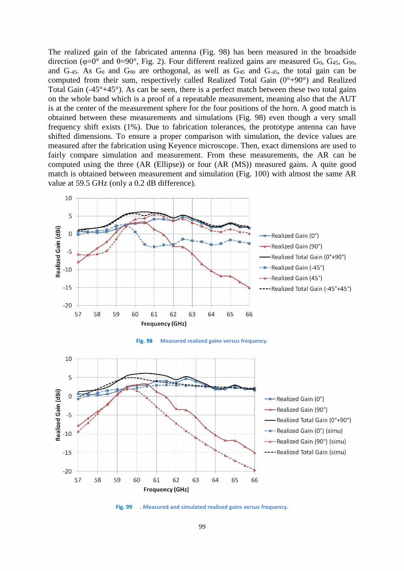
99
The realized gain of the fabricated antenna (Fig. 98) has been measured in the broadside
direction (φ=0° and θ=90°, Fig. 2). Four different realized gains are measured G0, G45, G90,
and G-45. As G0 and G90 are orthogonal, as well as G45 and G-45, the total gain can be
computed from their sum, respectively called Realized Total Gain (0°+90°) and Realized
Total Gain (-45°+45°). As can be seen, there is a perfect match between these two total gains
on the whole band which is a proof of a repeatable measurement, meaning also that the AUT
is at the center of the measurement sphere for the four positions of the horn. A good match is
obtained between these measurements and simulations (Fig. 98) even though a very small
frequency shift exists (1%). Due to fabrication tolerances, the prototype antenna can have
shifted dimensions. To ensure a proper comparison with simulation, the device values are
measured after the fabrication using Keyence microscope. Then, exact dimensions are used to
fairly compare simulation and measurement. From these measurements, the AR can be
computed using the three (AR (Ellipse)) or four (AR (MS)) measured gains. A quite good
match is obtained between measurement and simulation (Fig. 100) with almost the same AR
value at 59.5 GHz (only a 0.2 dB difference).
Fig. 98 Measured realized gains versus frequency.
Fig. 99 . Measured and simulated realized gains versus frequency.
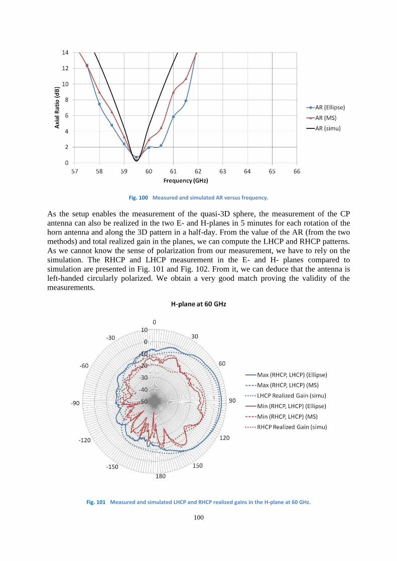
100
Fig. 100 Measured and simulated AR versus frequency.
As the setup enables the measurement of the quasi-3D sphere, the measurement of the CP
antenna can also be realized in the two E- and H-planes in 5 minutes for each rotation of the
horn antenna and along the 3D pattern in a half-day. From the value of the AR (from the two
methods) and total realized gain in the planes, we can compute the LHCP and RHCP patterns.
As we cannot know the sense of polarization from our measurement, we have to rely on the
simulation. The RHCP and LHCP measurement in the E- and H- planes compared to
simulation are presented in Fig. 101 and Fig. 102. From it, we can deduce that the antenna is
left-handed circularly polarized. We obtain a very good match proving the validity of the
measurements.
Fig. 101 Measured and simulated LHCP and RHCP realized gains in the H-plane at 60 GHz.

101
Fig. 102 Measured and simulated LHCP and RHCP realized gains in the E-plane at 60 GHz.
Fig. 103 presents the 3D measurement of the total realized gain with still a very good match
between the realized total gain (0°+90°) and realized total gain (-45°+45°). The maximum
achieved total realized gain for (0°+90°) and (-45°+45°) are 7.1 dB and 6.9 dBi respectively
in the direction (ϕ, θ) = (-10°, 88°). The 3D measurement of the AR is presented in Fig. 103
with the Ellipse and MS methods respectively. A rectangular plot was chosen for more clarity.
The blank parts are just out of range values. The AR is minimum around the broadside
direction (ϕ, θ)=(0°,90°). Ellipses computed from the method are super-imposed with the 3D
diagram. A good match is again obtained between simulation and measurement proving the
accuracy and usefulness of the method.
(a) (b) (c)
Fig. 103 Measured AR by (a) the Ellipse method and (b) the MS method compared to simulation (c).
The comparison between the two methods has still to be implemented and their accuracy be
computed, but both method give quite satisfactory results.

102
5. Radiation Efficiency
Another important issue when dealing with antenna measurement is the measurement of
antenna efficiency which is maybe one of the most important parameter of an antenna.
Several methods have been developed at lower frequencies for connector-fed antennas.
a) Typical Ways to Measure Radiation Efficiency
From [IEE93], the radiation efficiency is the ratio of the total power radiated by an antenna to
the net power accepted by the antenna from the connected transmitter (Equ. 23). The gain and
directivity are then related by the radiation efficiency.
The first thing that comes to mind to measure the efficiency is to deduce it from gain and
directivity measurements, where the radiation efficiency (ηR) is defined as the ratio of the
peak gain to the peak directivity (Equ. 22). But, this method does not give accurate results,
especially for directive antennas, because of the difficulty in calculating directivity from the
measured patterns with sufficient accuracy.
R
peak gain
peak directivity (Equ.22)
Other solutions include the Wheeler Cap method [WHE59] or the use of a reverberation
chamber [KIL04]. But, they are quite difficult to implement at Mmw frequencies, especially
because of the presence of the probe. They would also need new measurements or a different
measurement setup.
b) Measurement of efficiency using the proposed measurement setup
The value extracted for the measurement setup, is the realized gain, defined by Equ. 23. We
can then deduce the incident power entering the antenna ( incP ), and compute the total
efficiency ( tote ) from Eq. 37 where radP can also be developed as in Equ. 24.
2
11.(1 )radmeas tot
inc
Pe e S
P (Equ.23)
2
0 0( , )sin( )radP U d d
(Equ.24)
Then, tote can be expressed from Equ. 25, which simplifies into Equ. 26. As we are measuring
the realized gain by steps in ϕ and θ, Equ. 26 can be re-arranged in Equ. 27 using discrete
points. A value of the gain is associated to an area of the sphere, the smaller the steps in ϕ and
θ, the smaller the numerical error.
2
0 0( , )sin( )
radtot
inc inc
U d dPe
P P
(Equ.25)
2
0 0
1, sin( )
4
radtot real
inc
Pe G d d
P
(Equ.26)
1 1
1. . ( , )sin( )
4
M Nrad
tot real j i i
j iinc
Pe G
P
(Equ.27)
But, in Equ. 26, ϕ and θ vary from 0 to 2π and 0 to π respectively, which corresponds to the
measurement of the total 3D sphere. However, in our measurement setup, this is not possible
due to the positioner. During the 3D measurement, 73.5% of the total sphere is measured with
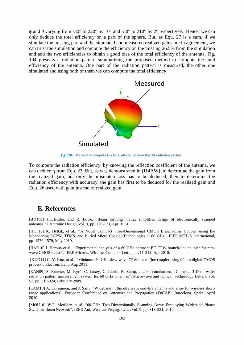
103
ϕ and θ varying from -30° to 220° by 10° and -30° to 210° by 2° respectively. Hence, we can
only deduce the total efficiency on a part of the sphere. But, as Equ. 27 is a sum, if we
simulate the missing part and the simulated and measured realized gains are in agreement, we
can trust the simulation and compute the efficiency on the missing 26.5% from the simulation
and add the two efficiencies to obtain a good idea of the total efficiency of the antenna. Fig.
104 presents a radiation pattern summarizing the proposed method to compute the total
efficiency of the antenna. One part of the radiation pattern is measured, the other one
simulated and using both of them we can compute the total efficiency.
Measured
Simulated
Fig. 104 Method to compute the total efficiency from the 3D radiation pattern.
To compute the radiation efficiency, by knowing the reflection coefficient of the antenna, we
can deduce η from Equ. 23. But, as was demonstrated in [J14AW], to determine the gain from
the realized gain, not only the mismatch loss has to be deduced, then to determine the
radiation efficiency with accuracy, the gain has first to be deduced for the realized gain and
Equ. 26 used with gain instead of realized gain.
E. References
[BUT61] J.L. Butler, and R. Lowe, "Beam forming matrix simplifies design of electronically scanned
antennas," Electronic Design, vol. 9, pp. 170-173, Apr. 1961.
[HET10] K. Hettak, et al., “A Novel Compact three-Dimensional CMOS Branch-Line Coupler using the
Meandering ECPW, TFMS, and Buried Micro Coaxial Technologies at 60 GHz”, IEEE MTT-S International,
pp. 1576-1579, May 2010.
[HAR10] I. Haroun et al., “Experimental analysis of a 60 GHz compact EC-CPW branch-line coupler for mm-
wave CMOS radios”, IEEE Microw. Wireless Compon. Lett., pp. 211-213, Apr 2010.
[KUO11] C.-Y. Kuo, at al., “Miniature 60 GHz slow-wave CPW branch(ine coupler using 90 nm digital CMOS
process”, Electron. Lett., Aug 2011.
[RAN09] S. Ranvier, M. Kyrö, C. Luxey, C. Icheln, R. Staraj, and P. Vainikainen, “Compact 3-D on-wafer
radiation pattern measurement system for 60 GHz antennas”, Microwave and Optical Technology Letters, vol.
51, pp. 319-324, February 2009.
[LAM10] A. Lamminen, and J. Saily, “Wideband millimetre wave end-fire antenna and array for wireless short-
range applications”, European Conference on Antennas and Propagation (EuCAP), Barcelona, Spain, April
2010.
[MOU10] W.F. Moulder, et al, “60-GHz Two-Dimensionally Scanning Array Employing Wideband Planar
Switched Beam Network”, IEEE Ant. Wireless Propag. Lett. , vol. 9, pp. 818-821, 2010.

104
[BAR10] M.H. Barakat, C. Delaveaud, and F. Ndagijimana, “60 GHz high resistivity silicon on insulator
interdigitated dipole antenna”, Microwave and Optical Technology Letters, vol. 52, no. 5, pp. 1197-1201, May
2010.
[LAN10] J. Lantéri, L. Dussopt, R. Pilard, D. Gloria, S.D. Yamamoto, A. Cathelin, and H. Hezzeddine, “60 GHz
antennas in HTCC and glass technology”, European Conference on Antennas and Propagation (EuCAP),
Barcelona, Spain, April 2010.
[MUR11] J. Murdock, E. Ben-Dor, F. Gutierrez, and T.S. Rappaport, “Challenges and approaches to on-chip
millimeter wave antenna pattern measurements”, IEEE International Microwave Symposium (MTT-S),
Baltimore, MA, June 2011.
[PIL09] R. Pilard, S. Montusclat, D. Gloria, F. Le Pennec, and C. Person, “Dedicated measurement setup for
millimetre-wave silicon integrated antennas: BiCMOS and CMOS high resistivity SOI process characterization”,
European Conference on Antennas and Propagation (EuCAP), Berlin, Germany, pp. 2447-2451, March 2009.
[ZWI04] T. Zwick, C. Baks, U.R. Pfeiffer, D. Liu, and B.P. Gaucher, “Probe based MMW antenna measurement
setup”, IEEE International Symposium on Antennas and Propagation (APS), Monterey, CA , pp. 747-750, June
2004.
[BEE10] S. Beer, and T. Zwick, “Probe based radiation pattern measurements for highly integrated millimeter-
wave antennas”, European Conference on Antennas and Propagation (EuCAP), Barcelona, Spain, April 2010.
[IEE79] “IEEE Standard Test Procedures for Antennas”, ANSI/IEEE 149-1979.
[WHE59] H. A. Wheeler, “The radiansphere around a small antenna,” Proceedings of the IRE, vol.47, pp. 1325-
1331, August 1959.
[KIL04] P-S. Kildal, and K. Rosengren, “Correlation and Capacity of MIMO Systems and Mutual Coupling ,
Radiation Efficiency, and Diversity Gain of their Antennas: Simulations and Measurements in a Reverberation
Chamber”, IEEE Communications Magazine, pp. 104-112, 2004.
[CHI10] T-Y. Chin, et al., “A V-band 8x8 CMOS Butler matrix MMIC”, IEEE Transactions on Microwave
Theory and Techniques, vol. 58, no. 12, pp. 3538-3546, December 2010.
[IEE93] “IEEE Standard Definitions of Terms for Antennas”, IEEE Std 145-1993, 1993.

105
IX. Research Perspectives
These years of research gave me the opportunity to work on ambitious projects within
talented senior researchers. Thanks to this great experience, it is time for me to develop my
own research subjects.
I believe that the Internet of Things is going to promote a new telecommunication domain
with the need of a completely different wireless infrastructure, maximizing sensitivity and
minimizing power consumption. The development of this research area will be assisted with
different project proposals.
My objective is to leverage my experience gained in millimeter wave systems and antenna
miniaturization to develop miniature and autonomous end point devices as well as to design
efficient and high capacity edge node gateways.
A. Motivation
The Internet of Things (IoT) refers to everything that is connected to the internet and that goes
beyond classical computers or mobile phones. According to a recent report by Cisco [CIS11],
it can be expected that over 50 billion objects will be connected to the internet by 2020. This
growth is creating unprecedented opportunities for industries, businesses and people.
Most of IoT systems are characterized by the transmission of small amounts of data at low
transmission rate, which drastically reduces the bandwidth requirements and leads to the
development of ultra-sensitive modulation schemes based on Ultra Narrow Band (UNB) (e.g.,
SigFox [SIG15]) or frequency spreading (e.g., LoRa [SEM15]) techniques. Usually, less than
1 MHz bandwidth is enough for most of the applications. Sub-GHz bands, such as the 868
MHz band in Europe and the 915 MHz band in the USA, are often preferred because of their
more reliable propagation characteristics.
IoT market is preparing to take off. Bouygues Telecom and Orange have announced the
deployment of a national network for 2016 based on LoRa technology. However, we have to
consider that LoRa, in its actual form, is just going to be the appetizer of IoT market. LoRa
technology has been chosen because it is the unique solution that combines extreme
sensitivity (-137dBm), ultra-low power consumption, bidirectional capability and high
security level (network and application 128-bit AES encryption keys). Moreover, the next
LoRa update will include localization using triangulation technique. On the other hand, LoRa
uses a derivative of Chirp Spread Spectrum modulation [LOR15] and to achieve the maximal
sensitivity, a time on air larger than 2 s is needed to transmit just a few Bytes. Considering
that thousands of connected objects will cohabit in the same cell, signal collisions will quickly
increase, especially if collided data are just re-transmitted. Nevertheless, the LoRa
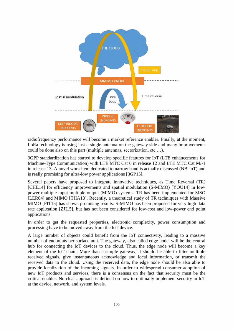
106
radiofrequency performance will become a market reference enabler. Finally, at the moment,
LoRa technology is using just a single antenna on the gateway side and many improvements
could be done also on this part (multiple antennas, sectorization, etc …).
3GPP standardization has started to develop specific features for IoT (LTE enhancements for
Machine-Type Communication) with LTE MTC Cat 0 in release 12 and LTE MTC Cat M/-1
in release 13. A novel work item dedicated to narrow band is actually discussed (NB-IoT) and
is really promising for ultra-low power applications [3GP15].
Several papers have proposed to integrate innovative techniques, as Time Reversal (TR)
[CHE14] for efficiency improvements and spatial modulation (S-MIMO) [YOU14] in low-
power multiple input multiple output (MIMO) systems. TR has been implemented for SISO
[LER04] and MIMO [THA13]. Recently, a theoretical study of TR techniques with Massive
MIMO [PIT15] has shown promising results. S-MIMO has been proposed for very high data
rate application [ZJI15], but has not been considered for low-cost and low-power end point
applications.
In order to get the requested properties, electronic complexity, power consumption and
processing have to be moved away from the IoT device.
A large number of objects could benefit from the IoT connectivity, leading to a massive
number of endpoints per surface unit. The gateway, also called edge node, will be the central
hub for connecting the IoT devices to the cloud. Thus, the edge node will become a key
element of the IoT chain. More than a simple gateway, it should be able to filter multiple
received signals, give instantaneous acknowledge and local information, or transmit the
received data to the cloud. Using the received data, the edge node should be also able to
provide localization of the incoming signals. In order to widespread consumer adoption of
new IoT products and services, there is a consensus on the fact that security must be the
critical enabler. No clear approach is defined on how to optimally implement security in IoT
at the device, network, and system levels.
107
B. Research proposal
In order to solve the different scientific challenges for IoT applications, I would like to
propose a new methodology to fulfill the IoT network requirements. It consists in moving all
the complexity and intelligence to the edge node side, and using ultra-low power technique on
the end point. MMIMO will be used on the edge node in order to increase sensitivity, to
enable signal processing to limit data collisions, and using channel information for end point
localization. Sub-GHz bands are targeted because of their better propagation and penetration
properties, leading to several challenges in the MMIMO antenna design. For the downlink,
the TR technique will be leveraged to focus the signal wave on the end point.
On the IoT device (end point), low-cost and low-power electronics will be associated with a
miniature and environment independent antenna. In order to maximize the uplink budget link,
S-MIMO at the endpoint level using reconfigurable super-directive antennas will be
optimized. A model of the entire network will be used to develop the suitable Medium Access
Control (MAC) layer and to develop innovative cryptographic techniques based on physical
layer information.
The goal of the project is to leverage this multi-factor approach to enable the connection of
100000 IoT devices on a 3km radius cell, with 5 to 10 payload transmissions per day.
Compared to actual M2M technology (LTE release 12), we are expecting a sensitivity
improvement of 20 to 30 dB, and an overall power consumption divided by 1000.
The different research activities of my project are divided in 3 different parts, addressing the
different levels of the system: Edge node, End Point and Network level.
1. Network level
A model of the entire network is essential to study complicated scenarios with a massive
number of devices. A network simulator (such as Omnet++) will be extended to take into
account the different techniques developed in the frame of the project. The model will be used
to quantify the impact of the different approaches on the network energy efficiency and
capacity. A dedicated MAC layer will be developed and optimized for a massive number of
end points. This work will be realized in close collaboration with LEAT MCSOC team.
MCSOC team will provide skills in modeling and design of autonomous systems. This
thematic will be integrated in CREMANT axis N°3.
A second part of this topic will consider the security aspect of the network, which is a critical
functionality for consumer adoption. We propose to leverage the disruptive approach based on
channel analysis to propose a Cryptographic Random Number generator based on channel
physical layer information, which has the potential to reduce the power consumption and the
cost at the secure end point side [FRA07]. A second security technique will use the unique
location-specific channel impulse response (CIS) signature to provide additional physical-
layer leveraging the TR technique. This topic will be lean on a collaboration with the System
and Software Security group in Eurecom.
2. Edge node level
The main motivation of this vision is the design of an asymmetrical network with all the
complexity moved at the edge node level. The use of a massive number of antennas will
increase the uplink sensitivity, and the downlink signal will be focused in time and space
domain using TR approach leveraging the reciprocity and multi-path characteristics of the

108
channel. Specific processing in order to decrease data collisions when a large number of IoT
devices are connected to a cell will be studied. Accurate channel models are a pre-requisite
for the MMIMO system design and performance evaluation. We plan to conduct channel
measurements with the Open Air Interface MMIMO testbed [JIA15]. It will provide a true full
MIMO channel including mutual coupling and the RF chain as it will be experienced by the
devices. Specific scenarios suitable for IoT applications such as deep indoor communication
will be targeted.
A second important part of this topic will be the MMIMO antenna design. The deployment of
reasonably sized sub-GHz edge Node with a very large number of antennas implies that these
antennas have to be densely packed, which raises obvious concerns about spatial correlation
(SC) and mutual coupling (MC) between radiating elements. Future UHF MMIMO antennas
must be strongly miniaturized by minimizing the single element size and decreasing the
coupling among the different elements. Different isolation techniques (Electromagnetic Band
Gap structure, neutralization technique) and size reduction methods (Artificial magnetic
conductor, parasitic elements) will be focused for array miniaturization. The optimal element
spacing distance in terms of efficiency, compactness and MIMO capabilities will be studied.
3. End point level
The end point RF has to be low power, low cost, and efficient in most of the situations. The
operating bandwidth required by IoT systems is usually very narrow, with one or few MHz
that are usually enough. In this framework, high antennas will be preferred and
consequently a new design approach based on the simoultaneous miniaturization of the
antenna and maximization of its radiation efficiency will be considered during the project. A
specific study will be dedicated to antenna fundamental limits on efficiency [GUS07]. First
results have shown that, in practical applications, the conductivity of the metal used to realize
the antenna must be carefully taken into account [LIZ15]. The modification of the
environment surrounding the antenna can cause a variation of its resonant frequency. This can
become a serious problem in dealing with narrow band antennas. In order to obtain radiating
structures that are independent on environment changes, the possibility of enclosing the UNB
antennas into isolating radomes will be investigated. A second approach consists in providing
the antenna with frequency reconfigurability. Towards this end, active components able to
reconfigure some antenna characteristics will be integrated into the antenna and used to
restore the antenna resonance to the desired frequency.
MIMO techniques have been largely used to improve link spectral efficiency. However,
spatial multiplexing using multiple antennas require one transmitter for each Tx antenna, and
complex processing, making it unusable for IoT devices due to the complexity and
consumption of the required hardware. However, because of the clear advantages of MIMO
techniques for channel capacity, new approaches for energy efficient multiple antenna
transmissions are needed. S-MIMO has the potential to provide MIMO key advantages with a
reduced hardware and power consumption cost. The basic principle is based on a
reconfigurable antenna with multiple radiation patterns, with the different radiation patterns
corresponding to the symbol of a spatial constellation diagram. This approach is adding a new
dimension to digital modulation schemes thanks to this spatial domain. From a hardware point
of view, a single RF chain is required with a fast RF switching unit, which is power efficient.
This solution could be leveraged to improve the budget link for up-link communication.
Considering that IoT technologies will preferably use sub-GHz band, some challenges arises
for the design of miniature reconfigurable antennas. In order to implement such MIMO
technique, several key research areas will be gathered as digital modulation, signal processing

109
at the transmitter and the receiver, link and channel modelling and super-directive antennas
[HAR58]. A reconfigurable super-directive antenna with beam steering capabilities will be
used at the end-point level and interfaced with the network testbed. Several approaches from
the simple spatial diversity, to more advanced spatial spreading codes will be studied.
C. Research Project Impact
The proposed project aspires to provide efficient IoT network solutions based on the
innovative TR and S-MIMO paradigm enabling the realization of highly efficient and secure
networks to support the increment of the number of connected objects expected for the next
years. The techniques proposed to obtain environment independent and energy efficient
antennas enable green, programmable and agile infrastructures capable of adapting to the
dynamic demands of different existing and future IoT applications as well as to reach energy
consumption levels that are economically and environmentally sustainable. This project, in
fact, represents the opportunity for me, within the SophiaTech campus, to promote
collaborations and shared activities between the different research centers (Eurecom, INRIA,
University Nice Sophia Antipolis). Moreover, this action fall into the Université of Côte
d’Azur initiative, that has been created in Feb. 2015 and gathers 13 different members (UNS,
INRIA, OCA, Skema, CHU, etc …). Finally, the University Côte d’Azur has won the highly
coveted “IDEX” award of the French Investments for the Future Program. The invested
capital of about 580 million euros that will be attributed to the UCA will generate 14.5 million
euros of interest income per year, meaning that a total of 58 million euros will be injected into
research, training, and innovation in the Côte d’Azur region over the next four years.
From the scientific point of view, the proposed research project is expected to have a strong
impact in the research community. Starting from the very limited requirements and
capabilities of IoT endpoint devices, the proposed approach of an asymmetric network
leveraging TR and S-MIMO techniques is completely new. This implies the need to face new
research challenges as the identification of upper bound limits on the antenna directivity, the
development of a more efficient and secure signal processing, and the study of an optimized
MAC layer to increase the overall network performance.
In order to broadcast the project results to a broader audience, F. Ferrero and L. Lizzi have
started the SOFIA (SOphia For Internet of Anything) Hub, a joint initiative of LEAT and the
Polytech Nice-Sophia engineering school of UNS aimed at promoting and supporting research
and teaching activities in the field of wireless communications for the Internet of Anything
(IoA) (www.sofiahub.unice.fr).
The IoT is an application domain that results are particularly suitable for technological
transfer. The telecommunication solutions developed during the project will be easily
exploited to strengthen already existing industrial and academic collaborations of LEAT and
will serve as building block to promote the creation of collaborative projects.
The proposed research project falls within the involved researchers’ idea of making the
SophiaTech campus the national reference for the research and teaching on IoT thanks to the
different subjects located on the campus, as the UCN@Sophia LABEX partners. This will
allow the study of all the IoT aspects, from the physical level of the single device (LEAT) to
network management and security issues (EURECOM) and the signal processing and
theoretical aspects (INRIA, I3S).

110
D. References
[3GP15] NarrowBand IOT, http://www.3gpp.org/news-events/3gpp-news/1733-niot, accessed Jan. 2016
[CAS14] Andrea Castagnetti, Alain Pegatoquet, Trong-Nhan Le and Michel Auguin, “A Joint Duty-Cycle and
Transmission Power Management for Energy Harvesting WSN”, IEEE Transactions on Industrial Informatics
Journal, Special section on “Industrial Wireless Sensor Networks”, Volume 10, Issue 2, pp. 928-936, May 2014.
[CIS11] D. Evans, “The internet of things. How the next evolution of the internet is changing everything”, Cisco
White Paper, 2011.
[CHE14] Yan Chen; Feng Han; Yu-Han Yang; Hang Ma; Yi Han; Chunxiao Jiang; Hung-Quoc Lai; Claffey, D.;
Safar, Z.; Liu, K.J.R., "Time-Reversal Wireless Paradigm for Green Internet of Things: An Overview," in
Internet of Things Journal, IEEE , vol.1, no.1, pp.81-98, Feb. 2014
[CHE14] Yan Chen; Feng Han; Yu-Han Yang; Hang Ma; Yi Han; Chunxiao Jiang; Hung-Quoc Lai; Claffey, D.;
Safar, Z.; Liu, K.J.R., "Time-Reversal Wireless Paradigm for Green Internet of Things: An Overview," in
Internet of Things Journal, IEEE , vol.1, no.1, pp.81-98, Feb. 2014
[CIS15] The Network: ‘Toronto Selected as Site for $100 Million Cisco Global Innovation Centre’,
http://newsroom.cisco.com/press-releasecontent? type=webcontent&articleId=1362116, accessed August 2015
[FRA07] Francillon, A.; Castelluccia, C., "TinyRNG: A Cryptographic Random Number Generator for Wireless
Sensors Network Nodes," in Modeling and Optimization in Mobile, Ad Hoc and Wireless Networks and
Workshops, 2007. WiOpt 2007. 5th International Symposium on , vol., no., pp.1-7, 16-20 April 2007
[GUS07] Mats Gustafsson, Christian Sohl, Gerhard Kristensson, "Physical limitations on antennas of arbitrary
shape", Proc. R. Soc. A 2007 463 2589-2607; DOI: 10.1098/rspa.2007.1893. Published 8 October 2007
[JIA15] Jiang, X.; Cirkic, M.; Kaltenberger, F.; Larsson, E. G.; Deneire, L. & Knopp, R., “MIMO-TDD
Reciprocity and Hardware Imbalances: Experimental Results”, CC 2015, IEEE International Conference on
Communications, 8-12 June 2015, London, United Kingdom
[JON15] M. Gustafsson, B. L. G. Jonsson, Antenna Q and stored energy expressed in the fields, currents, and
input impedance, IEEE Transactions on Antennas and Propagation, vol. 63(1) pages 240-249, 2015.
[HAR58] R. F. Harrington, “On the gain and beamwidth of directional antennas,” IEEE Trans. Antennas
Propag., vol. 6, no.3, pp. 219-225, Jul. 1958.
[LER04] G Lerosey, J De Rosny, A Tourin, A Derode, “Time reversal of electromagnetic waves”, Physical
review letters, 2004
[LOR15] AN1200.22LoRa™ Modulation Basics, Application note, Revision 2, May 2015,
www.semtech.com.
[LIZ11] L. Lizzi and A. Massa, “Dual-band printed fractal monopole antenna for LTE applications,” IEEE
Antennas and Wireless Propagation Letters, vol. 10, pp. 760-763, 2011
[LIZ15]L. Lizzi and F. Ferrero, “On the use of UNB Miniature Antennas for IoT Applications”, Electr. Lett.,
2015.
[PIT15] Pitarokoilis, A.; Mohammed, S.K.; Larsson, E.G., "Uplink Performance of Time-Reversal MRC in
Massive MIMO Systems Subject to Phase Noise," in Wireless Communications, IEEE Transactions on , vol.14,
no.2, pp.711-723, Feb. 2015
[SEM15] Semtech Investor News: ‘Bouygues Telecom Announces June Launch of France’s First "Internet-of-
Things" Network Based on LoRa Technology’,
http://investors.semtech.com/releasedetail.cfm?ReleaseID=904103, accessed August 2015
[SIG15] Gigacom Research: ‘Sigfox brings its internet of things network to San Francisco’,
https://gigaom.com/2014/05/20/sigfox-brings-its-internet-ofthings-network-to-san-francisco/, accessed August
2015
[THA13] Vu, Tran Ha; Hieu, Nguyen Thanh; Tam Linh, Ho Duc; Dung, Nguyen Thuy; Van Tuan, Le, "Channel
capacity of multi user TR-MIMO-UWB communications system," in Computing, Management and
Telecommunications (ComManTel), 2013 International Conference on , vol., no., pp.22-26, 21-24 Jan. 2013

111
[TLE14] T-N. Le, A. Pegatoquet, O. Berder, O. Sentieys and A. Carer, “Energy Neutral Design Framework for
Supercapacitor-based Autonomous Wireless Sensor Networks”, to appear in ACM Journal on Emerging
Technologies in Computing Systems (JETC), 2014.
[YOU14] Yousefbeiki, M.; Alrabadi, O.N.; Perruisseau-Carrier, J., "Efficient MIMO Transmission of PSK
Signals With a Single-Radio Reconfigurable Antenna," in Communications, IEEE Transactions on , vol.62, no.2,
pp.567-577, February 2014
[ZJI15] Zhiyuan Jiang; Molisch, A.F.; Caire, G.; Zhisheng Niu, "Achievable Rates of FDD Massive MIMO
Systems With Spatial Channel Correlation," in Wireless Communications, IEEE Transactions on , vol.14, no.5,
pp.2868-2882, May 2015

112
XI. BIBLIOGRAPHY
REVUES INTERNATIONALES AVEC COMITE DE LECTURE
[J05AW] F. Ferrero, C. Luxey, G. Jacquemod & R. Staraj, «Dual-Band circularly polarized microstrip antenna
for satellite applications», IEEE Antennas and Wireless Propagation Letters, vol. 4, 2005, p. 13-15
[J07EL] F. Ferrero, C. Luxey, R. Staraj, G. Jacquemod, V. Fusco, «Compact quasi-lumped hybrid coupler
tunable over a large frequency band», Electronic letters, Vol. 43, No. 19, 2007, p.1030-1031
[J09AP] F. Ferrero, C. Luxey, R. Staraj, G. Jacquemod, M. Yedlin, V. Fusco, "A Novel Quad-Polarization Agile
Patch Antenna", Antennas and Propagation, IEEE Transactions on , vol.57, no.5, pp.1563-1567, May 2009
[J09MO] F. Ferrero, C. Luxey, R. Staraj, G. Jacquemod, M. Yedlin, V. Fusco, "Theory and design of a tunable
quasi-lumped quadrature coupler", MOTL, Vol. 51, No. 9, September 2009
[J09EL] F. Ferrero, C. Luxey, R. Staraj, G. Jacquemod, M. Yedlin, V. Fusco, "Patch antenna with linear
polarisation tilt control", Electronic letters, Vol. 45, No. 17, August 2009
[J09MJ] B. Nicolle, R. Khouri, F. Ferrero, W. Tatinian, L. Carpineto, G. Jacquemod, "On the use of behavioral
modeling within the RFIC design flow: Satellite receiver case study", Microelectronic Journal, Vol. 40, 2009,
1726-1735.
[J09RE] F. Ferrero, A. Diallo, C. Luxey, B. Derat, P. Hamouz, P. Hazdra, J. Rahola, "Two-Element PIFA Array
Structure for Polarization Diversity in UMTS Mobile Phones ", Radioengineering, Vol. 18, N°4, Dec 2009, pp.
407-412.
[J11MO] F. Canneva, F. Ferrero, J. M. Ribero, and R. Staraj, « FREQUENCY RECONFIGURABLE
ANTENNA FOR DVB-H APPLICATIONS », MOTL, Vol. 53, No. 8, August 2011.
[J11AW] F. Ferrero, A. Chevalier, J. M. Ribero, R. Staraj, J. L. Mattei, and Y. Queffelec, “A New Magneto-
Dielectric Material Loaded, Tunable UHF Antenna for Handheld Devices”, IEEE AWPL, Vol. 10, pp. 951-954,
Sept. 2011.
[J11MO2] F. Canneva, F. Ferrero, J. M. Ribero, and R. Staraj, « Small reconfigurable PIFA for DVB-H
applications », MOTL, Vol. 53, No. 10, October 2011.
[J11TM] J.-L. Mattei, P. Queffelec, L. Huitema, J.-F. Pintos, Ph. Minard, A. Sharaiha; B. Jamnier, F. Ferrero, R.
Staraj, D. Souriou, A. Thakur, "Suitability of Ni-Zn Ferrites Ceramics with Controlled Porosity As Granular
Substrates for Mobile Handset Miniaturized Antennas", IEEE Trans. On Magnetics., Vol. 47, Iss. 10, pp. 3720-
3723, Oct. 2011.
[J12MO] D. Titz, M. Kyrö, F. Ferrero, S. Ranvier, C. Luxey, P. Brachat, G. Jacquemod and P. Vainikainen,”
Calibration methodology for a 3D radiation pattern set-up of probe-fed millimeter-wave antennas”, Microwave
and Optical Technology Letters, Volume 54, Issue 5, May 2012, Pages: 1183–1189
[J12MO2]L. Lizzi, F. Ferrero, J. Ribero, and R. Staraj, “Low-Profile Tetra Wire-Patch Antenna For Automotive
Applications”, Microwave and Optical Technology Letters, Volume 54, Issue 7, July 2012, Pages: 1711–1714.
[J12RE] D.Titz, F. Ben Abdeljelil, S. Jan, F. Ferrero, C. Luxey, P. Brachat, G. Jacquemod, “Design and
Characterization of CMOS On-Chip Antennas for 60 GHz Communications”, Radioengineering, Vol. 21, N°1,
Apr 2012, pp. 324-332.
[J12AW] Titz, D.; Pilard, R.; Gianesello, F.; Ferrero, F.; Luxey, C.; Brachat, P.; Jacquemod, G.; Gloria, D.,
“Industrial HTCC Antenna-Module SiP for 60-GHz Applications” , IEEE AWPL, Vol. 11, pp. 576-579, 2012.
[J12EL] Trinh L.H, Hoang T.Q.V, Ferret F., Ferrero F., "Improving wake-up receiver’s sensitivity by using a
novel architecture", Electronics Letters, Vol. 48, Iss. 11, pp. 559-560, May 2012
[J12MO3] Diane Titz, Fabien Ferrero, Romain Debroucke, Romain Pilard,Cyril Luxey ,Frederic Gianesello,
Sebastien Jan, Daniel Gloria, and Gilles Jacquemod, “MILLIMETER-WAVE MINIATURIZED HYBRID

113
COUPLERS INTEGRATED ON ADVANCED BiCMOS TECHNOLOGY”, Microwave and Optical
Technology Letters, Vol. 54, No. 10, October 2012.
[J12MO4] M. Silva Pimenta, F. Ferrero, R. Staraj and J.M. Ribero, “Low-profile circularly polarized GNSS
antenna”, Microwave and Optical Technology Letters, Volume 54, Issue 12, December 2012, Pages: 2811–2814
[J12AM] D. Titz, F. Ferrero, C. Luxey, “Development of a Millimeter-Wave Measurement Setup and Dedicated
Techniques to Characterize the Matching and Radiation Performance of Probe-Fed Antennas”, IEEE Antennas
and Propagation Magazine, Vol. 54, Iss. 4, August 2012, pp. 188-203.
[J12AW2] L. Lizzi, F. Ferrero, J. M. Ribero, R. Staraj, “Light and Low-Profile GSM Omnidirectional Antenna”,
IEEE AWPL, Vol. 11, pp. 1146-1149, 2012.
[J12AW3] D. Titz, F. Ferrero, P. Brachat, G. Jacquemod, C. Luxey, “Efficiency Measurement of Probe-Fed
Antennas Operating at Millimeter-Wave Frequencies”, IEEE AWPL, Vol. 11, pp. 1194-1197, 2012.
[J13AP] B. Zhang, Y. P. Zhang, D. Titz, F. Ferrero, C. Luxey, “A Circularly-Polarized Array Antenna Using
Linearly-Polarized Sub Grid Arrays for Highly-Integrated 60-GHz Radio”, IEEE Transactions on Antennas &
Propagation, Vol. 61, Iss. 1, pp. 436-439, January 2013.
[J13AP2] Hoang, T.Q.V.; Seguenot, E.; Ferrero, F.; Dubard, J.-L.; Brachat, P.; Desvilles, J.-L., "3D Voltage
Pattern Measurement of a 2.45 GHz Rectenna," Antennas and Propagation, IEEE Transactions on , vol.61, no.6,
pp.3354,3356, June 2013
[J13CP] Bing Zhang; Titz, D.; Ferrero, F.; Luxey, C.; Yue Ping Zhang, "Integration of Quadruple Linearly-
Polarized Microstrip Grid Array Antennas for 60-GHz Antenna-in-Package Applications," Components,
Packaging and Manufacturing Technology, IEEE Transactions on , vol.3, no.8, pp.1293,1300, Aug. 2013
[J13EL] Cihangir, A.; Sonnerat, F.; Ferrero, F.; Pilard, R.; Gianesello, F.; Gloria, D.; Brachat, P.; Jacquemod,
G.; Luxey, C., "Neutralisation technique applied to two coupling element antennas to cover low LTE and GSM
communication standards," Electronics Letters , vol.49, no.13, pp., June 20 2013
[J13MO] Florian Canneva, Fabien Ferrero, Alexis Chevalier, Jean-Marc Ribero, Jean-Luc Mattei, Patrick
Queffelec, Robert Staraj, “Miniature Reconfigurable Antenna with Magneto Dielectric Substrate for DVB-H
Band”, Microwave and Optical Technology Letters, Volume 55, Issue 9, pages 2007–2011, September 2013
[J13EL] Bisognin, A.; Titz, D.; Ferrero, F.; Luxey, C.; Jacquemod, G.; Pilard, R.; Gianesello, F.; Gloria, D.;
Brachat, P., "Differential feeding technique for mm-wave series-fed antenna-array," Electronics Letters , Vol.49,
No.15, July 18 2013
[J13AP3] Tu Zhihong; Zhang, Y.P.; Luxey, C.; Bisognin, A.; Titz, D.; Ferrero, F., "A Ceramic Antenna for Tri-
Band Radio Devices," Antennas and Propagation, IEEE Transactions on , vol.61, no.11, pp.5776,5780, Nov.
2013
[J13AP4] W. Zhang, Y.P Zhang, M. Sun, C. Luxey, D. Titz, F. Ferrero, "A 60-GHz Circularly-Polarized Array
Antenna-in-Package in LTCC Technology," Antennas and Propagation, IEEE Transactions on , vol.61, no.12,
Dec. 2013
[J13AW] A. Cihangir; W. Whittow, Panagamuwa, C.; Ferrero, F.; Jacquemod, G.; Gianesello, F.; Luxey, C.,
"Feasibility study of 4G cellular antennas for eyewear communicating devices," Antennas and Wireless
Propagation Letters, 2013.
[J14MO] D. Titz, F. Ferrero, R. Debroucke, R. Pilard, C. Luxey, F. Gianesello, S. Jan, D. Gloria, et G.
Jacquemod, “Millimeter-Wave Miniaturized Couplers Integrated on BiCMOS Technology”, Microwave and
Optical Technology Letters, vol. 56, no. 3, pp. 587-590, January 2014.
[J14AW] D. Titz; R. Pilard; F. Ferrero, F. Gianesello; D. Gloria, G. Jacquemod, C. Luxey, "Improved
Measurement Accuracy of Probe-Fed mm-Wave Antennas Using the Three Method," Antennas and Wireless
Propagation Letters, IEEE , vol.13, no., pp.103,105, 2014
[J14AW2] A. Cihangir; F. Ferrero, G. Jacquemod, P. Brachat, C. Luxey, "Neutralized Coupling Elements for
MIMO Operation in 4G Mobile Terminals," Antennas and Wireless Propagation Letters, IEEE , vol.13,
pp.141,144, 2014
[J14AW3] Bisognin, A.; Thielleux, J.; Wei, W.; Titz, D.; Ferrero, F.; Brachat, P.; Luxey, C., "Inkjet Coplanar
Square Monopole on flexible substrate for 60 GHz applications," Antennas and Wireless Propagation Letters,
IEEE , no.99, pp.1,1
114
[J14CP] Titz, D.; Ferrero, F.; Pilard, R.; Laporte, C.; Jan, S.; Ezzeddine, H.; Gianesello, F.; Gloria, D.;
Jacquemod, G.; Luxey, C., "New Wideband Miniature Branchline Coupler on IPD Technology for Beamforming
Applications," Components, Packaging and Manufacturing Technology, IEEE Transactions on , vol.4, no.5,
pp.911,921, May 2014
[J14MA] Lizzi, Leonardo; Ferrero, Fabien; Ribero, Jean-Marc; Staraj, Robert: 'Simple antenna structure
enabling the simultaneous excitation of two different polarisation and radiation modes', IET Microwaves,
Antennas & Propagation, 2014
[J14AW] Bisognin, A.; Titz, D.; Ferrero, F.; Jacquemod, G.; Pilard, R.; Gianesello, F.; Gloria, D.; Brachat, P.;
Laporte, C.; Ezzeddine, H.; Luxey, C., "PCB Integration of a Vivaldi Antenna on IPD Technology for 60-GHz
Communications," Antennas and Wireless Propagation Letters, IEEE , vol.13, no., pp.678,681, 2014
[J14FE] A. Cihangir, F. Ferrero, G. Jacquemod, P. Brachat, C. Luxey "Integration of Resonant and Non-
Resonant Antennas for Coverage of 4G LTE Bands in Handheld Terminals", Forum for Electromagnetic
Research Methods and Application Technologies (FERMAT), Vol. 3, 2014
[J14EL] Addaci, R.; Hamdiken, N.; Fortaki, T.; Ferrero, F.; Seetharamdoo, D.; Staraj, R., "Simple bandwidth-
enhancement technique for miniaturised low-profile UWB antenna design," Electronics Letters , vol.50, no.22,
pp.1564,1566, 10 23 2014.
[J15FE] A. Cihangir, F. Sonnerat, F. Ferrero, G. Jacquemod, F. Gianesello, R. Pilard, D. Gloria, P. Brachat, C.
Luxey, "LTE/4G Handset Antennas Realized with LDS Technology", Forum for Electromagnetic Research
Methods and Application Technologies (FERMAT), Vol. 9, 2015.
[J15AW] Semkin, V.; Ferrero, F.; Bisognin, A.; Ala-Laurinaho, J.; Luxey, C.; Devillers, F.; Raisanen, A.V.,
"Beam switching conformal antenna array for mm-wave communications," in Antennas and Wireless
Propagation Letters, IEEE.
[J15AW2] Chen, Z.; Zhang, Y.; Bisognin, A.; Titz, D.; Ferrero, F.; Luxey, C., "A 94 GHz Dual-Polarized
Microstrip Mesh Array Antenna in LTCC Technology," in IEEE Antennas and Wireless Propagation Letters,
2015
[J15AP] Bisognin, A.; Titz, D.; Ferrero, F.; Jacquemod, G.; Pilard, R.; Gianesello, F.; Gloria, D.; Lugara, D.;
Lima, E.B.; Costa, J.R.; Fernandes, C.A.; Luxey, C., "Noncollimating MMW Polyethylene Lens Mitigating
Dual-Source Offset From a Tx/Rx WiGig Module," in IEEE Transactions on Antennas and Propagation, vol.63,
no.12, pp.5908-5913, Dec. 2015
[J15EL] Lizzi, L.; Ferrero, F., "Use of ultra-narrow band miniature antennas for internet-of-things applications,"
in Electronics Letters , vol.51, no.24, pp.1964-1966, 11 19 2015
[J15AW3] Le Huy Trinh, Fabien Ferrero, Leonardo Lizzi, Jean-Marc Ribero and Robert Staraj, “Reconfigurable
Antenna for Future Spectrum Reallocations in 5G Communications”, in IEEE Antennas and Wireless
Propagation Letters, November 2015
[J15IJ] Le Huy Trinh, Fabien Ferrero, Leonardo Lizzi, Jean-Marc Ribero and Robert Staraj, “4x4 MIMO
MULTIBAND ANTENNA SYSTEM FOR MOBILE HANDSETS" IJAP, International Journal of Antennas and
PropagationVolume 2015 (2015), Article ID 857876, 1 November 2015
CONFERENCES INTERNATIONALES A COMITES DE LECTURE SUR
INVITATION DANS UNE SESSION SPECIALE OU CONVENUE:
[I07EU] F. Ferrero, C. Luxey, R. Staraj, G. Jacquemod, V. Fusco, «Linearly-Polarized tunable Antenna»,
European Conference on Antennas and Propagation (EuCAP 2007), November 2007, Edinburgh, UK, ISBN 92-
9092-937-5
[I09EU] F. Ferrero, A. Diallo, C. Luxey, B. Derat, "Pattern Diversity versus Polarization Diversity in UMTS
Mobile Phones", Proc. Eucap 2009, 3rd European Conference on Antennas & Propagation, 23-27 March 09,
Berlin, Germany.
[I09IW] F. Ferrero, A. Diallo, C. Luxey, B. Derat, "Phased Two-Element PIFA for Adaptative Pattern in UMTS
Handsets", Proc. IEEE International Workshop on Antenna Technology: "Small Antennas and Novel
Metamaterials (IWAT2009), 2-4 March 2009, Santa Monica, California (USA).

115
[I12EU] Aykut Cihangir, Fabien Ferrero, Cyril Luxey, Gilles Jacquemod, “A Novel Multi-Band Antenna Design
with Matching Network for Use in Mobile Terminals”, EUCAP , Pragues, Avril 2012.
[I12EU] Diane Titz, Fabien Ferrero, Cyril Luxey, Gilles Jacquemod, Claire Laporte, Hilal Ezzeddine, “Antenna-
in-Package Using PCB and IPD Technologies for 60 GHz Applications”, EUCAP, Pragues, Avril 2012.
[I12LA] Diane Titz, Fabien Ferrero, Gilles Jacquemod, Patrice Brachat, Cyril Luxey, “Measurement System for
Mm-wave Integrated and Probe-fed Antennas”, LAPC, Loughborough, Nov 2012.
[I12EU] Bisognin, Aimeric; Titz, Diane; Ferrero, Fabien; Luxey, Cyril; Jacquemod, Gilles; Brachat, Patrice;
Laporte, Claire; Ezzeddine, Hilal; Pilard, Romain; Gianesello, Frederic; Gloria, Daniel, "IPD technology for
passive circuits and antennas at millimeter-wave frequencies," Antennas and Propagation (EuCAP), 2013 7th
European Conference on , vol., no., pp.326,329, 8-12 April 2013
[I13EU] Cihangir, Aykut; Ferrero, Fabien; Luxey, Cyril; Jacquemod, Gilles; Brachat, Patrice, "A bandwidth-
enhanced antenna in LDS technology for LTE700 and GSM850/900 standards," Antennas and Propagation
(EuCAP), 2013 7th European Conference on , vol., no., pp.2786,2789, 8-12 April 2013
[I13EU] Bisognin, Aimeric; Titz, Diane; Ferrero, Fabien; Luxey, Cyril; Jacquemod, Gilles; Brachat, Patrice;
Laporte, Claire; Ezzeddine, Hilal, "D-band Quasi-Yagi antenna in IPD process," Antennas and Propagation
(EuCAP), 2013 7th European Conference on , vol., no., pp.330,331, 8-12 April 2013
[I14CA] F. Ferrero, C. Buey, J-M. Fargeas, P. Ratajczak, K. Bashir, L. H. Trinh, "Design of a Dual-Band MIMO
Wifi Gateway", IEEE CAMA 2014, November 2014, Antibes, France
[I14CA] L. Lizzi, P. Perrissol, F. Ferrero, P. Le Thuc, R. Staraj, "Experimental Validation of a Miniature
Implantable RFID Tag Antenna for Small Animals Monitoring", IEEE CAMA 2014, November 2014, Antibes,
France
[I14CA] T. Q. V. Hoang, L. H. Trinh, F. Ferrero, E. Seguenot, T-P. Vuong, J-L. Dubard, "Rectenna
Measurement in a Realistic Environment", IEEE CAMA 2014, November 2014, Antibes, France
[C15EU3] L.H. Trinh, Fabien Ferrero, J.M. Ribero, R. Staraj ,"Reconfigurable Antenna for Extension of LTE
Operational Mode Over TV White Spaces", Eucap, April 2015, Libon, Portugal
CONGRES INTERNATIONAUX AVEC COMITE DE LECTURE ET ACTES
[C04JI] F. Ferrero, C. Luxey, G. Jacquemod & R. Staraj, «Circularly Polarized Dual-Band Microstrip Antenna»,
JINA 04, Nice, 2004, p. 472-473,
[C05AC] F. Ferrero, C. Luxey, G. Jacquemod & R. Staraj, «A Circularly Polarized Dual-Band Microstrip
Antenna», IEEE/ACES ICWCACE, Honolulu, 2005, p. 942-945,
[C05AN] F. Ferrero, C. Luxey, G. Jacquemod, R. Staraj, G. Kossiavas & V. Fusco, «Reconfigurable phase-
arrays based on hybrid couplers in reflection mode», Antem 05, Saint-Malo, 2005, p. 244-245
[C06SA] S. Ranvier, F. Ferrero, C. Luxey, G. Jacquemod, R. Staraj, C. Icheln & P. Vainikainen, «Integrated
MIMO Antenna with Directional Diversity in the 60 GHz Band», SAME 06, Sophia Antipolis, 2006
[C06EU] F. Ferrero, C. Luxey, G. Jacquemod, R. Staraj & V. Fusco, «A reconfigurable hybrid coupler circuit
for agile polarisation antenna», EuCAP, Nice, 2006, ISBN 92-9092-937-5
[C06IC] F. Ferrero, S. Ranvier, C. Icheln, P. Vainikainen, C. Luxey, R. Staraj & G. Jacquemod, «Integrated
MM-Wave MIMO Antenna with Directional Diversity using MEMS Technology», ICECS 06, Nice, 2006, p.
447-450
[C07IW] F. Ferrero, C. Luxey, G. Jacquemod, R. Staraj & V. Fusco, «Polarisation-Reconfigurable Patch
Antenna», IWAT, Cambridge, 2007, p. 73-76
[C07IM] F. Ferrero & G. Jacquemod, «A tunable quasi-lumped microstrip coupler and RF applications», IMS,
Honolulu, 2007, p. 1197-1200
[C08HS] B. Nicole, F. Ferrero, L. Ferrero, L. Zastrow, Y. Herve, «From the UVA to the lipid chain reaction:
archetype of a virtual skin model», HSC'08, Huntsville, Octobre 2008.
[C09EU] Ferrero, F. Diallo, A. Luxey, C. Derat, B. , " Pattern diversity versus polarization diversity in UMTS
mobile phones ", Eucap, Berlin, pp. 1522, ISBN 978-1-4577-0250-1, Mars 2009.

116
[C09AP] F. Ferrero, C. Luxey, M. Yedlin, R. Staraj, G. Jacquemod, «Array-Antenna of Microstrip Patches Fed
by a Tunable Quasi-Lumped Hybrid Coupler». Proc. IEEE Antennas and Propagation Society International
Symposium (APS 2009), Charleston, June 1-5; 2009.
[C10AP] F. Canneva, F. Ferrero, J-M. Ribero, R. Staraj, «Reconfigurable miniature antenna for DVB-H standard
». Proc. IEEE Antennas and Propagation Society International Symposium (APS 2010), Toronto, July; 2010.
[C10AP2] F. Ferrero, F. Perret, J-M. Ribero, R. Staraj, «Self-Adjustable Circularly Polarized Patch Antenna ».
Proc. IEEE Antennas and Propagation Society International Symposium (APS 2010), Toronto, July; 2010.
[C11EU] Canneva, F. Ferrero, F. Chevalier, A. Ribero, J.M. Staraj, R. Mattei, J.L. Queffelec, P., " Miniature
reconfigurable antenna with magneto dielectric substrate for DVB-H band", Eucap, pp. 2289, ISBN 978-1-4577-
0250-1 , Avril 2011.
[C11EU2] Ferrero, F. Chevalier, A. Ribero, J.M. Staraj, R. Mattei, J.L. Queffelec, P. , "Influence of a magneto-
dielectric resonator on DVB-H antenna performances", Eucap, Rome, pp. 2156, ISBN 978-1-4577-0250-1 ,
Avril 2011.
[C11EU3] Oikonomopoulos-Zachos, C. Titz, D. Martinez-Vazquez, M. Ferrero, F. Luxey, C. Jacquemod, G. , "
Accurate characterisation of a 60 GHz antenna on LTCC substrate ", Eucap, Rome, pp. 3117, ISBN 978-1-4577-
0250-1, Avril 2011.
[C11NC] Titz, D.; Ferrero, F.; Luxey, C.; Jacquemod, G.; Debroucke, R.; Pilard, R.; Gianesello, F.; Gloria, D.,
"Reflection-type phase shifter integrated on advanced BiCMOS technology in the 60 GHz band," in New
Circuits and Systems Conference (NEWCAS), 2011 IEEE 9th International , vol., no., pp.434-437, 26-29 June
2011
[C11AP] Diane Titz, Fabien Ferrero, Cyril Luxey, Gilles Jacquemod, “A Novel Fully-Automatic 3D Radiation
Pattern Measurement Setup for 60 GHz Probe-Fed Antennas”, IEEE APS, Spokane, July 2011.
[C11AP2] Romain Pilard, Frédéric Gianesello, Daniel Gloria, Diane Titz, Fabien Ferrero, Cyril Luxey, “60 GHz
HR SOI CMOS Antenna for a System-on-Chip Integration Scheme Targeting High Data-Rate Kiosk
Applications”, IEEE APS, Spokane, July 2011.
[C11AP3] Florian Canneva, Fabien Ferrero, Jean-Marc Ribero, Robert Staraj, “New Reconfigurable Small
Antenna for DVB-H and GPS Standard”, IEEE APS, Spokane, July 2011.
[C11IM] D. Titz, R. Pilard, F. Ferrero, F. Gianesello, D. Gloria, C. Luxey, P. Brachat, G. Jacquemod, “60GHz
Antenna Integrated on High Resistivity Silicon Technologies Targeting WHDMI Applications”, IMS, Baltimore,
June 2011.
[C11LA] Jean‐Luc Fournier; Diane Titz; Fabien Ferrero; Cyril Luxey; Eric Dekneuvel; Gilles Jacquemod,
“Phased Array Antenna Controlled by Neural Network FGPA”, LAPC, Loughborough, Nov 2011.
[C11LA2] Diane Titz; Mikko Kyrö; Fabien Ferrero; Sylvain Ranvier ;Cyril Luxey; Patrice Brachat; Gilles
Jacquemod , Pertti Vainikainen, “Measurement Setup and Associated Calibration Methodology for 3D Radiation
Pattern of Probe‐fed Millimeter‐wave Antennas”, LAPC, Loughborough, Nov 2011.
[C12IW] Diane Titz, Fabien Ferrero, Cyril Luxey, Patrice Brachat, Gilles Jacquemod, “Radiation Pattern
Characterization of Antennas at Millimeter‐Wave Frequencies”, IWAT 2012, Tucson, March 2012
[C12IW2] Oumy Diop , Fabien Ferrero, Aliou Diallo, Gilles Jacquemod, Claire Laporte, Hilal Ezzeddine, Cyril
Luxey, “Planar Antennas on Integrated Passive Device Technology for Biomedical Applications”, IWAT 2012,
Tucson, March 2012
[C12EU] Marcio Silva Pimenta, Fabien Ferrero, Patrice Brachat, Philippe Ratajczak, Robert Staraj, Jean Marc
Ribero, “Textile Artificial Magnetic Conductor for GPS Applications”, EUCAP, Pragues, Avril 2012.
[C12EU2] Akiko Kohmura, Jerome Lanteri, Fabien Ferrero, Claire Migliaccio, Philippe Ratajczak, Shunichi
Futatsumori, Naruto Yonemoto, “Ka-band Dual Frequency Switchable Reflect array”, EUCAP,Pragues, Avril
2012.
[C12AN] Addaci Rafik, Ferrero Fabien, Diallo aliou, Lethuc Philippe, Staraj Robert, Crisan Nicolae, Cremene
Ligia, Luxey Cyril, “Design of multi-antenna diversity system dedicated to interrogation in noisy propagation
environments”, ANTEM, Toulouse, Juin 2012
[C12IM] D. Titz, F. Ferrero, R. Pilard, C. Laporte, S. Jan, H. Ezzeddine, F. Gianesello, D. Gloria, C. Luxey, and
G. Jacquemod, “New Wideband Integrated Miniature Branchline Coupler for Beamforming Applications”, IEEE
IMS, Montreal, Canada, Juin 2012

117
[C12AP] Leonardo Lizzi, Fabien Ferrero, Jean-Marc Ribero, and Robert Staraj, “Compact Low-Profile
Omnidirectional Surface Wave Antenna for UMTS Applications”, IEEE APS, Chicago, Juillet 2012
[C12AP2] Diane Titz, Fabien Ferrero, Cyril Luxey, Gilles Jacquemod, “A Fast and Accurate Method to Measure
the Radiation Characteristics of Probe-fed Circularly-Polarized Antennas in Mm-Wave Bands”, IEEE APS,
Chicago, Juillet 2012
[C12AP3] F. Ferrero, J.M. Ribero and R. Staraj, “Chassis engineering to enlarge the bandwidth for GSM-450
application”, IEEE APS, Chicago, Juillet 2012
[C12AP4] Jennifer M. Edwards, Gabriel M. Rebeiz, Diane Titz, Fabien Ferrero, Cyril Luxey, “High-Efficiency
Elliptical-Slot Silicon RFIC Antenna with Quartz Superstrate”, IEEE APS, Chicago, Juillet 2012
[C12AP5] Diane Titz, Fabien Ferrero, Cyril Luxey, Gilles Jacquemod, Claire Laporte, Hilal Ezzeddine, “Design
of a Miniaturized Butler Matrix in IPD Process for 60 GHz Switched-Beam Antenna Arrays”, IEEE APS,
Chicago, Juillet 2012
[C12AP6] R. Pilard, D. Titz, F. Gianesello, P. Calascibetta, J.M. Rivière, J. Lopez, R. Coffy, E. Saugier, A.
Poulain, F. Ferrero, C. Luxey, P. Brachat, G. Jacquemod and Daniel Gloria, “HDI Organic Technology
Integrating Built-In Antennas Dedicated to 60 GHz SiP Solution”, IEEE APS, Chicago, Juillet 2012.
[C12IS] Akiko Kohmura, Jérôme Lanteri, Fabien Ferrero, Claire Migliaccio, Shunichi Futatsumori, Naruto
Yonemoto, “Ka-band Beam Switchable Fresnel Reflector”, ISAP 2012, Nagoya, Japan, October 2012.
[C12SA] Oumy Diop, Fabien ferrero, Aliou Diallo, Gilles Jacquemod, Claire Laporte, Hilal Ezzeddine, Cyril
Luxey, “ IPD technology for co-integration of balun and miniature antennas at 2.4 GHz ” , Sophia Antipolis
Micro-Electronics Conference SAME 2012, 2-3 Octobre 2012, Sophia Antipolis, France.
[C12LA] Aykut Cihangir; Florence Sonnerat; Fabien Ferrero; Cyril Luxey; Romain Pilard; Frederic Gianesello;
Gilles Jacquemod, “Design of Traditional and a Novel Space-Efficient Antenna- Coupling Elements for Lower
LTE/GSM Mobile Phones”, LAPC, Loughborough, Nov 2012.
[C12LA2] Diane Titz; Bisognin Aimeric; Fabien Ferrero; Cyril Luxey; Gilles Jacquemod; Claire Laporte; Hilal
Ezzeddine; Mario Valente; Patrice Brachat, “60 GHz Patch Antenna Using IPD Technology”, LAPC,
Loughborough, Nov 2012.
[C12LA3] Florence Sonnerat; Romain Pilard; Frederic Gianesello; Daniel Gloria; François Le Pennec; Christian
Person; Aykut Cihangir; Fabien Ferrero; Cyril Luxey; Patrice Brachat, “Wideband LDS Antenna Using Two
Radiating Elements”, LAPC, Loughborough, Nov 2012.
[C13JS] Jiashu Chen; Lu Ye; Titz, D.; Gianesello, F.; Pilard, R.; Cathelin, A.; Ferrero, F.; Luxey, C.; Niknejad,
A.M., "A digitally modulated mm-Wave cartesian beamforming transmitter with quadrature spatial combining,"
Solid-State Circuits Conference Digest of Technical Papers (ISSCC), 2013 IEEE International , vol., no.,
pp.232,233, 17-21 Feb. 2013
[C13IW] Cihangir, A.; Ferrero, F.; Luxey, C.; Jacquemod, G., "A space-efficient coupling element antenna for
WWAN applications," Antenna Technology (iWAT), 2013 International Workshop on , pp.55,58, 4-6 March
2013
[C13EU] Semkin, Vasilii; Kyro, Mikko; Kolmonen, Veli-Matti; Luxey, Cyril; Bisognin, Aimeric; Ferrero,
Fabien; Happy, Henri; Raisanen, Antti V., "Conformal antenna array for 60 GHz applications," Antennas and
Propagation (EuCAP), 2013 7th European Conference on , pp.605,608, 8-12 April 2013
[C13EU2] Lizzi, Leonardo; Ferrero, Fabien; Ribero, Jean-Marc; Staraj, Robert, "Design of light and low-profile
antennas for vehicular applications," Antennas and Propagation (EuCAP), 2013 7th European Conference on ,
pp.1281,1284, 8-12 April 2013.
[C13AP] Bisognin, Aimeric; Luxey, Cyril; Jacquemod, Gilles; Ferrero, Fabien; Titz, Diane; Thielleux, Julien;
Wei, Wei; Happy, Henri; Brachat, Patrice, "Antenna on PEN substrate for millimeter-wave applications,"
Antennas and Propagation Society International Symposium (APSURSI), 2013 IEEE , pp.684,685, 7-13 July
2013.
[C13AP2] Bisognin, Aimeric; Luxey, Cyril; Jacquemod, Gilles; Titz, Diane; Ferrero, Fabien; Pilard, Romain;
Gianesello, Frederic; Gloria, Daniel; Brachat, Patrice, "A new symmetric feeding technique for a broadband
series-fed antenna-array," Antennas and Propagation Society International Symposium (APSURSI), 2013 IEEE ,
pp.2183,2184, 7-13 July 2013.
118
[C13AP3] Lizzi, Leonardo; Ferrero, Fabien; Ribero, Jean-Marc; Staraj, Robert, "Low-profile multimode antenna
for vehicular applications," Antennas and Propagation Society International Symposium (APSURSI), 2013 IEEE
, pp.2069,2070, 7-13 July 2013
[C13AP4] Trinh, L.H.; Ferrero, F.; Staraj, R.; Ribero, J.-M., "700–960MHz MIMO antenna for picocell
applications," Antennas and Propagation Society International Symposium (APSURSI), 2013 IEEE ,
pp.366,367, 7-13 July 2013
[C13AP5] Cihangir, Aykut; Ferrero, Fabien; Luxey, Cyril; Jacquemod, Gilles; Sonnerat, Florence; Pilard,
Romain; Gianesello, Frederic; Gloria, Daniel; Brachat, Patrice, "Combination of two neutralized coupling
element antennas for low LTE and GSM mobile phones,"Antennas and Propagation Society International
Symposium (APSURSI), 2013 IEEE , pp.2215,2216, 7-13 July 2013
[C13AP6] Bisognin, Aimeric; Luxey, Cyril; Jacquemod, Gilles; Titz, Diane; Ferrero, Fabien; Bisognin, Aimeric;
Pilard, Romain; Gianesello, Frederic; Gloria, Daniel; Laporte, Claire; Ezzeddine, Hilal; Brachat, Patrice, "End-
fire radiating antenna on IPD technology for 60 GHz communications," Antennas and Propagation Society
International Symposium (APSURSI), 2013 IEEE , pp.1830,1831, 7-13 July 2013
[C13LA] Cihangir, Aykut; Ferrero, Fabien; Luxey, Cyril; Jacquemod, Gilles; Larique, Emmanuel; Robin,
Renaud; Brachat, Patrice, "Tunable antennas using MEMS switches for LTE mobile terminals," Antennas and
Propagation Conference (LAPC), 2013 Loughborough , pp.22,26, 11-12 Nov. 2013.
[C13LA2] Semkin, Vasilii; Kyro, Mikko; Raisanen, Antti V.; Bisognin, Aimeric; Ferrero, Fabien; Luxey, Cyril;
Happy, Henri; Thielleux, Julien; Wei, Wei, "Characterization of inkjet patch antenna on different ground planes
at millimeter-wave frequencies," Antennas and Propagation Conference (LAPC), 2013 Loughborough ,
pp.286,288, 11-12 Nov. 2013
[C13AT] L. H. Trinh, F Ferrero, R. Staraj, J-M. Ribero, “Mobile Phone Antenna for 2G, 3G and 4G Standards”,
ATC’2013, Ho Chi Minh City, 16-18 October 2013, Vietnam
[C14IW] Aykut Cihangir, Fabien Ferrero, Cyril Luxey,Gilles Jacquemod, Alexandre Reinhardt, Laurent
Dussopt, Nicolas Lorphelin, Christophe Pavageau ,Patrice Brachat, "Utilization of Tunable Components for 4G
Frequency Reconfigurable Mobile Terminal Antenna", IWAT 2014, Sydney, Australia
[C14EU] Cihangir, Aykut; Ferrero, Fabien; Luxey, Cyril; Jacquemod, Gilles; Reinhardt, Alexandre; Dussopt,
Laurent; Lorphelin, Nicolas; Obeid, Nizar; Brachat, Patrice, "Investigation of tunable matching circuits for
multiband 4G handsets," Antennas and Propagation (EuCAP), 2014 8th European Conference on , pp.601,604,
6-11 April 2014, The Hague, The Netherlands.
[C14EU2] Bisognin, Aimeric; Titz, Diane; Ferrero, Fabien; Jacquemod, Gilles; Pilard, Romain; Gianesello,
Frederic; Gloria, Daniel; Laporte, Claire; Ezzeddine, Hilal; Lugara, Delphine; Luxey, Cyril, "Probe-fed
measurement system for F-band antennas," Antennas and Propagation (EuCAP), 2014 8th European Conference
on , pp.722,726, 6-11 April 2014, The Hague, The Netherlands.
[C14EU3] Semkin, Vasilii; Jacob, Martin; Kurner, Thomas; Bisognin, Aimeric; Ferrero, Fabien; Luxey, Cyril;
Raisanen, Antti V., "Estimation of optimum antenna configurations supported by realistic propagation models at
60 GHz," Antennas and Propagation (EuCAP), 2014 8th European Conference on , pp.3434,3438, 6-11 April
2014, The Hague, The Netherlands.
[C14AP] Cihangir, A; Jacquemod, G.; Luxey, C.; Ferrero, F.; Whittow, W.G.; Panagamuwa, C.J.; Pilard, R.;
Gianesello, F., "MIMO antenna concept for 4G electronic eyewear devices," Antennas and Propagation Society
International Symposium (APSURSI 2014), Memphis, USA.
[C14AP2] Bisognin, A; Titz, D.; Luxey, C.; Jacquemod, G.; Pilard, R.; Gianesello, F.; Gloria, D.; Ferrero,
Fabien; Lugara, Delphine; Costa, Jorge R.; Fernandes, Carlos A, "Comparizon of 3D printed Plastic and
micromachined Teflon Lenses for WiGig modules," Antennas and Propagation Society International Symposium
(APSURSI), 2014 IEEE , pp.109,110, 6-11 July 2014, Memphis, USA.
[C14AP3] Lizzi, Leonardo; Trinh, Le Huy; Ferrero, Fabien; Pegatoquet, Alain; Ribero, Jean-Marc; Staraj,
Robert, "Synthesis of miniature pattern-reconfigurable antennas for smart wireless sensor nodes," Antennas and
Propagation Society International Symposium (APSURSI), 2014 IEEE , pp.1443,1444, 6-11 July 2014,
Memphis, USA.
[C15EU] Venkatasubramanian, Sathya N.; Li, Linsheng; Icheln, Clemens; Ferrero, Fabien; Luxey, Cyril;
Haneda, Katsuyuki, "Impact of neutralization on isolation in co-planar and back-to-back antennas," in Antennas
and Propagation (EuCAP), 2015 9th European Conference on , vol., no., pp.1-5, 13-17 April 2015, Lisbon,
Portugal

119
[C15EU2] A. Bisognin Aimeric, F. Ferrero, D. Titz, G. Jacquemod, R. Pilard, F. Gianesello, D. Gloria, C.
Laporte and H. Ezzeddine, P. Ratajczak, J.R. Costa, E.B. Lima, C.A. Fernandes, C. Luxey ,"Performance
Evaluation of a 120 GHz 3DPrinted Plastic Elliptical Lens AntennaSystem", Eucap, April 2015, Lisbon,
Portugal
[C15AP] F. Baurreau, R. Staraj, F. Ferrero, L. Lizzi, J. M. Ribero and J. P. Chessel, "Stratospheric platform for
telecommunication missions," Antennas and Propagation & USNC/URSI National Radio Science Meeting, 2015
IEEE International Symposium on, Vancouver, BC, 2015, pp. 914-915.
[C15AP2] F. Ferrero and L. Lizzi, "Feasability of an Ultra narrow band antenna for the internet of things,"
Antennas and Propagation & USNC/URSI National Radio Science Meeting, 2015 IEEE International
Symposium on, Vancouver, BC, 2015, pp. 776-777.
[C15AP3] Le Huy Trinh, F. Ferrero, R. Staraj and J. M. Ribero, "Influence of component ESR on a 4G
frequency reconfigurable antenna," Antennas and Propagation & USNC/URSI National Radio Science Meeting,
2015 IEEE International Symposium on, Vancouver, BC, 2015, pp. 1136-1137.
[C15AP4] L. Lizzi, Le Huy Trinh, F. Ferrero, J. M. Ribero and R. Staraj, "Transmision line based approach for
the synthesis of pattern reconfigurable antennas," Antennas and Propagation & USNC/URSI National Radio
Science Meeting, 2015 IEEE International Symposium on, Vancouver, BC, 2015, pp. 2369-2370.
CONGRES NATIONAUX AVEC COMITE DE LECTURE ET ACTES
[C05JN] Ferrero, C. Luxey, G. Jacquemod, R. Staraj, G. Kossiavas & V. Fusco, «Antennes réseaux à déphaseurs
actifs», JNM 05, Nantes, 2005
[C07JN] Ferrero, C. Luxey, R. Staraj, G. Jacquemod & V. Fusco, «Coupleur reconfigurable pour antenne à
diversité de polarisation», JNM 07, Toulouse, 2007
[C09JN] Ferrero, A. Diallo, C. Luxey, B. Derat, «Système multi-antennes alimenté par déphaseur reconfigurable
pour diversité en téléphonie mobile UMTS», Journées Nationales Microondes JNM 09, 27-29 Mai 2009,
Grenoble. Présentation orale C. Luxey.
[C09JN2] F. Ferrero, S. Ranvier, C. Luxey, C. Icheln, P. Vainikainen, R. Staraj, G. Jacquemod, «Réseau
déphaseur à base de commutateurs MEMS pour antennes millimétriques intégrées agiles en rayonnement» ,
Journées Nationales Microondes JNM2009, 27-29 Mai 2009, Grenoble.
[C11JN] M. Silva Pimenta, F. Ferrero, J. M. Ribero, R. Staraj, " Antenne à polarisation circulaire pour les
standards GPS-Galileo ", Journées Nationales Microondes JNM2011, Mai 2011, Brest.
[C11JN2] Diane Titz, Fahd Ben Abdeljelil, Sébastien Jan, Fabien Ferrero, Cyril Luxey, Patrice Brachat, Gilles
Jacquemod" Antennes Intégrées pour des Communications à 60 GHz, Journées Nationales Microondes
JNM2011, Mai 2011, Brest.
[C11JN3] Diane Titz, Fabien Ferrero, Romain Debroucke, Romain Pilard, Cyril Luxey, Frédéric Gianesello,
Daniel Gloria, Gilles Jacquemod, " Miniaturisation de coupleurs sur Substrat Silicium pour Applications en
bande Millimétrique ", Journées Nationales Microondes JNM2011, Mai 2011, Brest.
[C11JN4] F. Canneva, F. Ferrero, J.-M. Ribero, R. Staraj, “ Antenne miniature reconfigurable en fréquence pour
les standards DVB-H et GPS”, GDR Ondes, Nice, Oct. 2011.
[C11JN5] Marcio Silva Pimenta, F. Ferrero, P. Ratajzack, P. Brachat, R. Staraj, J. M. Ribero, “ Conducteur
Magnétique Artificiel sur substrat textile pour le standard GPS”, GDR Ondes, Nice, Oct. 2011.
[C11JN6] L.H. Trinh, T.Q.V. Hoang, F. Perret, F.Ferrero, “ Conception d'une rectenna à 433 mhz pour réseau de
capteurs”, GDR Ondes, Nice, Oct. 2011.
[C13JN] Bisognin Aimeric, Titz Diane, Ferrero Fabien, Luxey Cyril, Jacquemod Gilles, Pilard Romain,
Gianesello Fréderic, Gloria Daniel, Brachat Patrice, « Banc de caractérisation d'antennes intégrées alimentées
sous pointes pour bandes de fréquences millimétriques », Journées Nationales Microondes JNM2013, Mai 2013,
Paris.
[C13JN2] Bisognin Aimeric, Titz Diane, Ferrero Fabien, Luxey Cyril, Jacquemod Gilles, Pilard Romain,
Gianesello Fréderic, Gloria Daniel, Laporte Claire, Ezzeddine Hilal, Valente Mario, Brachat Patrice, « Patch en
technologie IPD reporté sur substrat organique pour des transferts de données courte portée à 60 GHz »,
Journées Nationales Microondes JNM2013, Mai 2013, Paris.

120
[C13JN3] Bisognin Aimeric, Titz Diane, Ferrero Fabien, Luxey, Cyril, Jacquemod Gilles, Pilard Romain,
Gianesello, Fréderic, Gloria Daniel, Brachat Patrice, « Nouvelle technique d'alimentation symétrique pour
réseaux d'antennes en bandes millimétriques », Journées Nationales Microondes JNM2013, Mai 2013, Paris.
[C13JN4] Bisognin Aimeric, Titz Diane, Ferrero Fabien, Luxey Cyril, Jacquemod Gilles, Pilard Romain,
Gianesello Fréderic, Gloria Daniel, Laporte Claire, Ezzeddine Hilal, Brachat Patrice, « Antenne-in-package à
rayonnement longitudinal pour standard WiGig », Journées Nationales Microondes JNM2013, Mai 2013, Paris.
[C13JN5] Bisognin Aimeric, Titz Diane, Ferrero Fabien, Luxey, Cyril, Jacquemod Gilles, Pilard Romain,
Gianesello Fréderic, Gloria Daniel, Laporte Claire, Ezzeddine, Hilal, Brachat Patrice, « Conception et
caractérisation d'antennes à 120 GHz en technologie IPD ™ », Journées Nationales Microondes JNM2013, Mai
2013, Paris.
[C13JN6] Bisognin Aimeric, Titz Diane, Thielleux Julien, Wei Wei, Happy Henri, Ferrero Fabien, Luxey Cyril,
Jacquemod Gilles, Brachat Patrice, « Conception et mesure d'une antenne à 60 GHz imprimée par jet d'encre sur
un substrat souple PEN », Journées Nationales Microondes JNM2013, Mai 2013, Paris.
[C13JN7] Ferrero Fabien, Diallo Aliou, Luxey Cyril, Derat Benoit, Hamouz Pavel, Hazdra Pavel, Rahola Jussi,
« Excitation des modes caractéristiques d'un PCB de téléphone mobile pour diversité de polarisation aux
fréquences UMTS », Journées Nationales Microondes JNM2013, Mai 2013, Paris.
[C13JN8] Cihangir Aykut, Ferrero Fabien, Luxey Cyril, Jacquemod Gilles, Brachat Patrice, « Conception d'un
nouvel élément antennaire de couplage pour terminaux mobiles LTE/UMTS/GSM », Journées Nationales
Microondes JNM2013, Mai 2013, Paris.
[C13JN9] Diane Titz, Ferrero Fabien, Cyril Luxey, Gilles Jacquemod, Romain Pilard, Fréderic Gianesello,
Claire Laporte, Hilal Ezzedine, Daniel Gloria, « Matrice de Butler en technologie IPD' pour formation de
faisceau à 60 GHz », Journées Nationales Microondes JNM2013, Mai 2013, Paris.
[C13JN10] Lizzi Leonardo, Ferrero Fabien, Ribero Jean-Marc, Staraj Robert, « Antenne multi-bandes
multimodes pour applications sur véhicules », Journées Nationales Microondes JNM2013, Mai 2013, Paris.
[C13JN11] Titz Diane, Ferrero Fabien, Luxey Cyril, Jacquemod Gilles, Pilard Romain, Gianesello Fréderic,
Gloria Daniel, « Coupleurs hybrides miniatures large bande en technologie BiCMOS pour circuits fonctionnant à
60 GHz », Journées Nationales Microondes JNM2013, Mai 2013, Paris.
[C13JN12] Le Huy Trinh, Emmanuel Le Guen, Fabien Ferrero, R. Staraj, Jean-Marc Ribero, Jean-Luc Mattei, «
Miniaturisation d'antenne IFA avec un matériau magnéto-diélectrique pour application LTE 700-GSM dans une
picocell », Journées Nationales Microondes JNM2013, Mai 2013, Paris.
[C13JN13] Aykut Cihangir, Florence Sonnerat, Fabien Ferrero, Romain Pilard, Frédéric Gianesello, Daniel
Gloria, Cyril Luxey, Gilles Jacquemod, Patrice Brachat, « Antenne en technologie LDS pour terminaux mobiles
LTE700 et GSM850/900 », Journées Nationales Microondes JNM2013, Mai 2013, Paris.
CONFERENCE D'ORDRE PEDAGOGIQUE
[C09JN] R. Staraj, S. Ranvier, F. Ferrero, P. Panaia, Ph. Le Thuc, C. Luxey, G. Jacquemod, P. Vainikainen,
"Reconfiguration dynamique d’antennes imprimées et composants radiofréquences micro-électromécaniques
MEMS RF", 16èmes Journées Nationales Microondes 2009, Journée thématique "De la RF au millimétrique sur
Silicium", 26 Mai 2009, Grenoble.
[C09JP] Fabien.Ferrero, Cyril.Luxey, Gregory. Sauder, Philippe. Lorenzini, Gilles. Jacquemod, " Radar doppler
hyperfrequences pour détection de vitesse ", JPCNFM, St Malo, Octobre 2009.
[C12JP] Stéphane MEILLÈRE, Fabien FERRERO, Philippe PANNIER, Gilles JACQUEMOD, " Réseaux de
Capteurs Intelligents RECAIN / WSN", JPCNFM, St Malo, Novembre 2012.
[C14JP] Miguel Angel García Pérez, Yves Leduc, Fabien Ferrero, " Re-imaginons les travaux pratiques pour la
formation ingénieurs en électronique ", JPCNFM, St Malo, Novembre 2014.
JOURNAL D'ORDRE PEDAGOGIQUE
[J15J3] Miguel Ángel García Pérez, Yves Leduc et Fabien Ferrero, “Re-imaginons les travaux pratiques pour la
formation des ingénieurs en électronique”, 7 août 2015, J3eA, Vol. 14, HORS SÉRIE 2 (2015).

121
PATENTS
[B09IM] BR36810/EP/GD, F. Ferrero, "Antenne multi-services à bande ultralarge incorporée dans un véhicule",
IMRA EUROPE SAS, Mars 2009
[B09IM2] BR37414/EP/GD/TM , F. Ferrero, "Antenne multi-services à bande ultra-large miniature", IMRA
EUROPE SAS, Juillet 2009