analysis and simulations of z-source inverter control methods
TRANSCRIPT

Analysis and Simulations of Z-Source Inverter Control Methods
B.Y. Husodo, M. Anwari, and S.M. Ayob Department of Energy Conversion Engineering
Faculty of Electrical Engineering, Universiti Teknologi Malaysia 81310 UTM Skudai, Johor Bahru, Malaysia
e-mail: [email protected]
Abstract –In this paper, two different control methods for Z-source inverter are examined. The Simple Boost and the Maximum Boost control methods of the inverter are analyzed and compared each other using simulation with MATLAB/Simulink. The Simple Boost control with independence relation between modulation index and shoot-through duty ratio is also simulated and analyzed. The selection of high modulation index and shoot-through duty ratio can reduce the inverter’s dc link voltage overshoot and increasing power delivery capacity of the inverter.
Keywords–Z-Source inverter; PWM; Control; Fuel Cell.
I. INTRODUCTION
Z-source inverter can boost dc input voltage with no requirement of dc-dc boost converter or step up transformer, hence overcoming output voltage limitation of traditional voltage source inverter as well as lower its cost. A comparison among conventional PWM inverter, dc-dc boosted PWM inverter, and Z-source inverter shows that Z-source inverter needs lowest semiconductors and control circuit cost, which are the main costs of a power electronics system [1]. This results in increasing attention on Z-source inverter, especially for the application where the input DC source has a wide voltage variation range, such as the photovoltaic (PV) grid-tied generation and fuel cell motor drive system [2]. Moreover, for Z-source inverter we have not to worry about EMI influence since shoot through are welcome and even exploited. This in turn enhances the inverter reliability.
There are various methods can be used to control Z-source inverter [3 – 9]. These can be classified into two categories according to the different shoot-through (ST) states insertion methods. The first category has the principle that ST states are generated by properly level shifting the modulation signals of voltage source inverter. ST states then will be inserted at every states transition, six ST state insertions in one switching cycle. The second category, in the other hand, directly replaces the
Taufik Electrical Engineering Department
Cal Poly State University San Luis Obispo, CA 93407, USA
email: [email protected]
null states (111 and 000) by ST states. There are two ST states insertion in one switching cycle of the second category. The comparison of these two categories shows that the second category has higher efficiency than the first category [2]. In this paper, two different ways of Z-source inverter control with two ST states insertion in one switching cycle (second category) will be examined and compared through simulation by MATLAB/ Simulink.
II. Z-SOURCE INVERTER
The configuration of 3-phase Z-source inverter is shown in Fig. 1. It consists of 2 identical inductors and 2 identical capacitors which are composed to form a unique impedance network to avoid short circuit when the devices are in shoot through mode, a diode to block reverse current, and a three phase bridge as in traditional inverter. In 3-phase Z-source inverter, one additional control parameter is introduced, namely the Boost Factor (B), which modifies the AC output voltage equation of traditional 3-phase PWM inverter as following.
2 VoBMvout =ˆ (1)
Where:
v̂out = Maximum sinusoidal inverter output voltage
B = Boost factor
M = Modulation Index
Vo = DC Input voltage
If we replace BM with G, then we may rewrite (1) as
978-1-4244-7398-4/10/$26.00 ©2010 IEEE IPEC 2010699
voutˆ 2
VoG= (2)
G is the inverter gain,
BMG = (3)
It can be seen that (2) has the same form with that of the traditional VSI, i.e.
Vov̂out = M (4)2
Boost Factor is obtained by introducing shoot through of minimally one pare of the inverter arm for a short period of time which called shoot-through time.
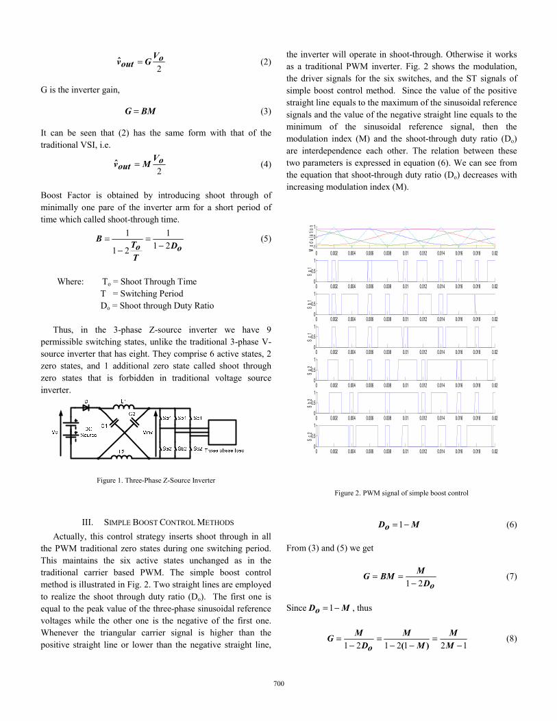
the inverter will operate in shoot-through. Otherwise it works as a traditional PWM inverter. Fig. 2 shows the modulation, the driver signals for the six switches, and the ST signals of simple boost control method. Since the value of the positive straight line equals to the maximum of the sinusoidal reference signals and the value of the negative straight line equals to the minimum of the sinusoidal reference signal, then the modulation index (M) and the shoot-through duty ratio (Do) are interdependence each other. The relation between these two parameters is expressed in equation (6). We can see from the equation that shoot-through duty ratio (Do) decreases with increasing modulation index (M).
M o
dula
t ion 1
0
-1
1 1B = = (5) To 1 − 2Do1 − 2 0 0.002 0.004 0.006 0.008 0.01 0.012 0.014 0.016 0.018 T 1
0.5
Where: To = Shoot Through Time 0 0 0.002 0.004 0.006 0.008 0.01 0.012 0.014 0.016 0.018
T = Switching Period 1
0.5 Sb1
S
a1
Do = Shoot through Duty Ratio S
c1
0 0 0.002 0.004 0.006 0.008 0.01 0.012 0.014 0.016 0.018
1
0.5 Thus, in the 3-phase Z-source inverter we have 9
permissible switching states, unlike the traditional 3-phase V-0
Sa2
0 0.002 0.004 0.006 0.008 0.01 0.012 0.014 0.016 0.018 source inverter that has eight. They comprise 6 active states, 2 1
0.5 zero states, and 1 additional zero state called shoot through zero states that is forbidden in traditional voltage source 0
0 0.002 0.004 0.006 0.008 0.01 0.012 0.014 0.016 0.018 inverter. 1
Sc2
S
b2
0.5
0 0 0.002 0.004 0.006 0.008 0.01 0.012 0.014 0.016 0.018
1
0.5
0 0 0.002 0.004 0.006 0.008 0.01 0.012 0.014 0.016 0.018
Figure 1. Three-Phase Z-Source Inverter
Figure 2. PWM signal of simple boost control
III. SIMPLE BOOST CONTROL METHODS = 1− M (6) Do Actually, this control strategy inserts shoot through in all
the PWM traditional zero states during one switching period. From (3) and (5) we get This maintains the six active states unchanged as in the traditional carrier based PWM. The simple boost control MG = BM = (7)method is illustrated in Fig. 2. Two straight lines are employed 1 − 2Do to realize the shoot through duty ratio (Do). The first one is equal to the peak value of the three-phase sinusoidal reference Since Do = 1− M , thus voltages while the other one is the negative of the first one. Whenever the triangular carrier signal is higher than the M M MG = = = (8)positive straight line or lower than the negative straight line, 1 − 2Do 1 − 2(1 − M ) 2M −1
700
0.02
0.02
0.02
0.02
0.02
0.02
0.02

Equation (8) infers that the inverter gain (G) can be controlled To π / 2(2 − M sin θ − M sin(θ − 2π / 3))= ∫ dθby adjusting modulation index (M). If we rearrange (1) in the T π / 6 2 original PWM output voltage equation form, we get 2π − π33
(13) =
2πBVov̂out = M (9)2 From (5) and (13),
BVo should be the dc input voltage of the traditional VSI 1 πB = = (14) which in the case of Z-source inverter is the dc voltage applied 33To M − π1 − 2to inverter bridge. T
Say The inverter voltage gain (G) is obtained as
BVo = (10) Vinv π πMG = BM = M = (15) 33 33M −π M −π
It can be seen from Fig. 1 that Vinv is the voltage stress of the inverter’s devices.
From (3) and (8),
Again, as with the simple boost control method, the voltage gain can be controlled by adjusting the modulation index.
Fig. 4 shows voltage gain as the function of modulation B = 2G −1 (11) index for both simple boost and maximum boost control
methods. It is clear from the figure that maximum boost Substitute (11) to (10), the voltage stress across the devices is control method gives higher voltage gain for the same modulation index. 1Vinv = (2G −1)Vo = Vo (12)
2M −1
1
0
-1Mod
u la
tion
IV. MAXIMUM BOOST CONTROL METHOD 0 0.002 0.004 0.006 0.008 0.01 0.012 0.014 0.016 0.018 1Maximum boost control method converts all traditional
Sc2
S
b2
Sa2
S
c1
Sb1
S
a1
0.5 zero states to shoot-through while maintaining the six active
0 0 0.002 0.004 0.006 0.008 0.01 0.012 0.014 0.016 0.018 states remain unchanged. This is obtained by comparing the
1
with the triangular carrier. Whenever the maximum is lower 0 0 0.002 0.004 0.006 0.008 0.01 0.012 0.014 0.016 0.018
than the triangular or the minimum is higher than the 1
maximum and the minimum curve of the sinusoidal reference 0.5
triangular, the inverter shoots through. Otherwise, it operates 0.5
0in the traditional PWM mode. By this control strategy the 0 0.002 0.004 0.006 0.008 0.01 0.012 0.014 0.016 0.018 1shoot-through duty cycle varies each cycle. The inverter gains
maximum shoot-through time which in turn gives the inverter higher boost factor, according to equation 5. Thus, with the same modulation index as in simple boost control method, we
0.5
0 0 0.002 0.004 0.006 0.008 0.01 0.012 0.014 0.016 0.018
1
0.5
0get higher voltage gain. Fig. 3 shows the maximum boost 0 0.002 0.004 0.006 0.008 0.01 0.012 0.014 0.016 0.018
control strategy. 1
0.5
As the shoot-through duty cycle varies each cycle, what we 0 0 0.002 0.004 0.006 0.008 0.01 0.012 0.014 0.016 0.018
are interested in is the average value of the duty cycle. In the interval (π/6, π/2), the average shoot through duty ratio can be expressed as following.
Figure 3. PWM signal of maximum boost control
701
0.02
0.02
0.02
0.02
0.02
0.02
0.02

Simple Boost
Maximum Boost
10
9
8
7
6
5
4
3
2
1
0 0.1 0.2 0.3 0.4 0.5 0.6 0.7 0.8 0.9 1
inverter whose modulation index and shoot-through duty ratio are independent of each other is carried out. This control strategy is done by setting the straight lines unequal to the peak maximum and minimum of the sinusoidal reference signals. Simulation is conducted using various values of shoot-through duty ratio (D0) and modulation index (M). The straight line value is normalized by the peak value of the triangular carrier wave. Initially, simulation is conducted by M equals 1.0 and D0 equals 0.45. Then simulation is carried on with M equals0.9, 0.55, and 0.4 while D0 remains at the same value.
Vol
tage
Gai
n (G
)
Modulation Index (M)
1
M o
du la
tionFigure 4. Voltage Gain versus Modulation Index
0
-1 0 0.002 0.004 0.006 0.008 0.01 0.012 0.014 0.016 0.018
1 0.5
0 0 0.002 0.004 0.006 0.008 0.01 0.012 0.014 0.016 0.018
Sa1
Obviously, the voltage stress across the inverter’s devices is
π 1 Vinv BVo Vo (16) = =
Sc2
S
b2
Sa2
S
c1
Sb1
0.5 3 3M −π
0 0 0.002 0.004 0.006 0.008 0.01 0.012 0.014 0.016 0.018
1
8 0.5
Simple Boost
Maximum Boost
0.5 1 1.5 2 2.5 3 3.5 4 4.5
7 0 0 0.002 0.004 0.006 0.008 0.01 0.012 0.014 0.016 0.018
6 1
norm
alis
ed d
evic
e vo
ltage
stres
s (V
inv/
Vo)
0.5 5
0 4 0 0.002 0.004 0.006 0.008 0.01 0.012 0.014 0.016 0.018
1 3
0.5 2
0 0 0.002 0.004 0.006 0.008 0.01 0.012 0.014 0.016 0.018
1 1
0 0.5
Voltage Gain (G)
Figure 5. Devices Voltage Stress
The voltage stress across the devices in obtaining a specified voltage gain for both the simple boost and the maximum boost control method is depicted in Fig. 5. From the figure, it is shown that the maximum boost control method can reduce the voltage stress across the inverter’s devices for the same voltage gain compared with the simple boost control. It means that for given devices, the inverter can obtain higher voltage gain.
V. OPERATION OF Z-SOURCE INVERTER UNDER SIMPLE BOOST CONTROL METHOD WITH INDEPENDENT RELATIONSHIP
BETWEEN THE MODULATION INDEX (M) AND THE SHOOT THROUGH DUTY RATIO (DO)
As was previously discussed, usually the simple boost control method is achieved by using a pair of straight line which are equal to the maximum peak and minimum peak of the reference sinusoidal, implying that the modulation index (M) and the shoot through duty ratio are related each other. The relationship is expressed by (6) as Do = 1− M . In the rest of this paper, simulation of simple boost operation of z-source
0 0 0.002 0.004 0.006 0.008 0.01 0.012 0.014 0.016 0.018
Figure 6. PWM signal of simple boost control with independent relationship between modulation index and shoot-though duty ratio
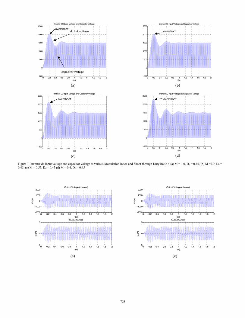
The simulation results will be discussed in the following part. Fig. 7 shows the inverter’s dc link voltage and the Z network’s capacitor voltage. We observe from the figure that the inverter builds equal steady state dc link voltage (Vinv) and capacitor voltage. However, there are variations in the value of voltage overshoot of the dc link voltage. As can be seen from Fig. 7, the lowest overshoot occurs when the modulation index and shoot-through duty ratio are high (Fig. 7a : M = 1.0, D0 = 0.45). Meanwhile, Fig. 8 shows the inverter’s ac output voltage and output current resulted from the simulation. It can be seen that the output voltage of the inverter are the same for all the conditions carried out through the simulation. Variation is observed in the output current delivered by the inverter. It is shown in Fig. 8 that the inverter delivers the highest output current when the modulation index is much higher than the straight line (Fig. 8a : M = 1.0, D0 = 0.45). Since the output
702
0.02
0.02
0.02
0.02
0.02
0.02
0.02
Inverter DC Input Voltage and Capacitor Voltage Inverter DC Input Voltage and Capacitor Voltage 2500 2500
overshoot 2000
1500
1000
500
0
dc link voltage
capacitor voltage
overshoot
2000
1500
1000
500
0
-500 -500 0 0.2 0.4 0.6 0.8 1 1.2 1.4 1.6 1.8 2 0 0.2 0.4 0.6 0.8 1 1.2 1.4 1.6 1.8 2
t(s) t(s)
(a) (b)
Inverter DCInput Voltage and Capacitor Voltage Inverter DC Input Voltage and Capacitor Voltage 2500 2500
overshoot
2000 2000
1500 1500
1000 1000
500500
00
-500 -500
overshoot
0 0.2 0.4 0.6 0.8 1 1.2 1.4 1.6 1.8
t(s) 0 0.2 0.4 0.6 0.8 1 1.2 1.4 1.6 1.8 2
t(s)
(c) (d)
Figure 7. Inverter dc input voltage and capacitor voltage at various Modulation Index and Shoot-through Duty Ratio : (a) M = 1.0, D0 = 0.45, (b) M =0.9, D0 = 0.45, (c) M = 0.55, D0 = 0.45 (d) M = 0.4, D0 = 0.45
Output Voltage (phase a) Output Voltage (phase a) 2000 2000
1000 1000
Vo(
V)
Vo(
V)
0 0
-1000 -1000
-2000 -2000 0 0.2 0.4 0.6 0.8 1 1.2 1.4 1.6 1.8 2 0 0.2 0.4 0.6 0.8 1 1.2 1.4 1.6 1.8 2
t(s) t(s) Output Current Output Current
5 5
Io (A
)
Io (A
)
00
-5 -5 0 0.2 0.4 0.6 0.8 1 1.2 1.4 1.6 1.8 2 0 0.2 0.4 0.6 0.8 1 1.2 1.4 1.6 1.8 2
t(s) t(s)
(a) (c)
703
2

2
Output Voltage (phase a) Output Voltage (phase a) 2000 2000
1000 1000
0 0
0 0.2 0.4 0.6 0.8 1 1.2 1.4 1.6 1.8 2 0 0.2 0.4 0.6 0.8 1 1.2 1.4 1.6 1.8
Vo(
V)
Vo(
V)
-1000 -1000
-2000 -2000
t(s) t(s) Output Current Output Current
4 4
2 2
0 0.2 0.4 0.6 0.8 1 1.2 1.4 1.6 1.8 2 0 0.2 0.4 0.6 0.8 1 1.2 1.4 1.6 1.8
Io (A
)
Io (A
)
0 0
-2 -2
-4 -4
t(s) t(s)
(b) (d) Figure 8. Output voltage and output current at various Modulation Index and Shoot-through Duty Ratio (a) M = 1.0, D0 = 0.45, (b) M =0.9, D0 = 0.45, (c) M = 0.55, D0 = 0.45 (d) M = 0.4, D0 = 0.45
voltages are equal, higher output current of the inverter means higher output power. Hence, according to the simulation results, for simple boost control of z- source inverter, it would be more advantageous to use high modulation index and high shoot-through duty ratio as the inverter would deliver higher output power with lower inverter’s dc input voltage overshoot.
CONCLUSION
Two control methods with two ST states insertion of Z-source inverter has been analyzed and compared in this paper. The boost factor, voltage gain, duty ratio, and voltage stress across the switches for each method have been analyzed in detail. Simulation of Z-source converter under simple control method using straight lines with the value different from the peak value of the sinusoidal reference has also been presented, showing that better performance would be obtained if modulation index (M) and shoot-through duty ratio (D0) are set to a high value.
ACKNOWLEGMENT
The authors would like to thank the Malaysian Ministry of Science, Technology, and Innovation (MOSTI) and the University Teknologi Malaysia (UTM) for sponsoring this work through the science fund grant.
REFERENCES
[1] M. Olzwesky, “Z-Source Inverter for Fuel Cell Vehicles”, U.S. Department of Energy, Freedom CAR and Vehicles Technologies, EE-2G, 1000 Independence Avenue, SW, Washington, D.C. 20585-0121, 2005, pp. 15-17.
[2] J. Li, J. Liu, and Z. Liu, “Loss Oriented Evaluation and Comparison of Z-Source Inverters Using Different Pulse Width Modulation Strategies”, in 2009 IEEE Applied Power Electronics Conference and Exposition.
[3] F.Z. Peng, M. Shen, and Z. Qiang, “Maximum Boost Control of the Z-Source Inverter”, IEEE Transactions on Power Electronics, vol. 20, no.4, pp. 833-838, July 2004.
[4] P.C. Loh, D.M. Vilathgamuwa, Y.S. Lai, G.T. Chua, and Y. Li, “Pulse-Width Modulation of Z-Source Inverter”, in Conf. Rec. 2004 IEEE Industry Applications Conferences, pp. 148-155.
[5] N. Muntean, L. Tutelea, and I. Boldea, “A Modified Carrier-Based PWM Modulation Technique in Z-Source Inverter”, in 2007 Int. Aegean Conf. on Electrical Machines and Power Electronics, pp. 174-180.
[6] Q.V. Tran, T.W. Chun, J.R. Ahn, and H.H. Lee, “Algorithms for Controlling Both the DC Boost and AC Output Voltage of Z-Source Inverter”, IEEE Transactions on Industrial Electronics, vol. 54, no. 5, October 2007.
[7] F. Z. Peng, "Z-source inverter", IEEE Transactions on Industry Applications, vol. 39, pp. 504-510, Mar-Apr 2003.
[8] J. B. Liu, J. G. Hu, and L. Y Xu, "A modified space vector PWM for z-source inverter - Modeling and design," ICEMS 2005, in Proceedings of the Eighth International Conference on Electrical Machines and Systems, Vols 1-3, pp. 1242-1247, 2005.
[9] M.S. Shen, J. Wang, A. Joseph, F.Z. Peng, L.M. Tolbert, and D.J. Adams, “ Constant Boost Control of the Z-source Inverter to Minimize current Ripple and Voltage Stress”, IEEE Transactions on Industry Applications, vol. 42, pp. 770 – 778, May-Jun 2006.
704
2