an fpga architecture supporting dynamically-controlled ...absoul/papers/slides/bsoul12altera.pdf ·...
TRANSCRIPT

An FPGA Architecture Supporting Dynamically-Controlled Power Gating
Altera CorporationMarch 16th, 2012
Assem Bsoul and Steve Wilton{absoul, stevew}@ece.ubc.ca
System-on-Chip Research GroupDepartment of Electrical and Computer Engineering
University of British ColumbiaVancouver, B.C., Canada

2
What this talk is about
An FPGA architecture supporting dynamic power gating:– Turn off regions at run-time to save power, with on-chip control
ASIC designers do this regularly
Challenges for an FPGA:– We don’t know about application– Routing for signals – Handling wakeup in
a programmable way control
System-on-chip with 2 islands

3
Motivation for new FPGA Arch.
FPGA leakage power is major component of total power– Almost the same amount as dynamic power for 28nm
• Cyclone V: Static 32%, Dynamic 42%, I/O 26%*
High-end FPGAs are power hungry– Entering an era where we can’t turn it all on at once!– Large power leads to heat issues reliability, cooling cost
Mobile hand-held applications– Many applications have regions with long idle periods
*Altera WP-01158-2.0: Meeting the Low Power Imperative at 28nm

4
Some Relevant Work

5
Statically-Controlled Power Gating
Available FPGA power gating is statically-controlled– Unused FPGA blocks are turned off at configuration time
Useful if amount of unused resources in FPGA is large!– However, designers select the smallest chip that fits their design
Frequently idle blocks still dissipate leakage!
Logic Cluster
VDD
SRAM

6
Commercial FPGAs
Programmable Power Technology (Stratix III, IV, V)– Change Vth of LABs according to location on critical path– Not runtime-controlled!
Power gating for embedded blocks– Shut down unused I/O, memories, PLLs, transceivers, etc.– Supported in both Altera and Xilinx– Done at configuration time
Flash*Freeze in IGLOO and ProASIC3L from Microsemi– Allows sleep mode for the whole chip
7
We propose an FPGA architecture where regions of the chip can be turned on/off at runtime to
control their power consumption

8
Outline
• Power gating architecture• Complications: wakeup current• System-level evaluation• Current work• Other issues
9
Outline
• Power gating architecture • Complications: wakeup current• System-level evaluation• Current work• Other issues

10
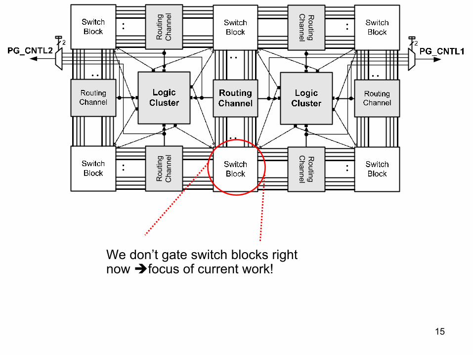
Our FPGA Architecture – Big Picture
Divide FPGA device into power-controlled regions– Support dynamically-controlled sleep mode
Use general-purpose routing fabric for control signals
Power domain
Power gating region
Power control signal

11
Architecture Details

12
Logic Cluster
Logic Cluster
VDD
201
LC power switch
PG_CNTL1

13
Routing
Channel
Routing
Channel
Rou
ting
Cha
nnel
Rou
ting
Cha
nnel
A routing channel is shared between the two neighboring logic clusters
Logic Cluster
In1
In3
Logic Cluster
In1
In3
In2
In4
In4
In2
Routing channel
Connection box
Track isolation buffer

14
Routing
Channel
Routing
Channel
Rou
ting
Cha
nnel
Rou
ting
Cha
nnel
VDDRouting channel power switch
201
Routing Channel
PG_CNTL1PG_CNTL2
Turn off routing channel only when both neighbors are off.
15
Routing
Channel
Routing
Channel
Rou
ting
Cha
nnel
Rou
ting
Cha
nnel
We don’t gate switch blocks right now focus of current work!
16
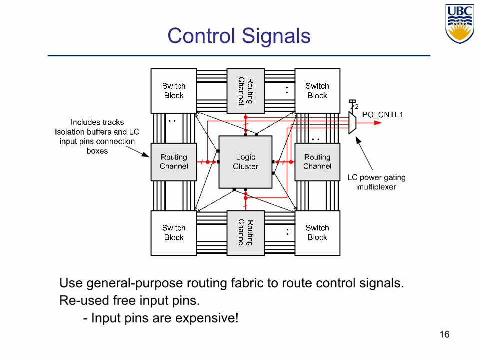
Control Signals
Use general-purpose routing fabric to route control signals.Re-used free input pins.
- Input pins are expensive!

17
Area Overhead: Region Power Gating
RC
RC
RC
RC
RC
RC
From
bor
derin
g co
nnec
tion
bloc
ksArchitecture granularity- Share sleep transistor among “region” of tiles.
Control signal from borderingrouting channels.
Interesting tradeoff:- Area vs. CAD difficulty Power gating region, size 2x2

18
Evaluation
– The Good: Potential leakage reduction
– The Bad: Area, Delay, Leakage power overhead

19
Experimental Setup
• Sweep architecture – N (cluster)– W (channel)– R (region)
• 45 nm PTM
• Three architectures– Ungated– Static-gating (SG)– Dynamic-gating (DG)
Create HSPICE netlist (automatic LC buffer
sizing)
Meets performance constraints (10%)?
Run HSPICE to measure performance
Create HSPICE netlist for power gating architecture
Collect results (leakage power and area)
Resize sleep transistors
Architecture parameters
(N, I, W, Fcout, ...)
Yes
No

20
Granularity Results: Leakage Power
• Compared to ungated, static-gating and dynamic-gating reduce leakage in sleep mode by more than 44%.
• Dynamic-gating has 0.8% more leakage than static-gating (R=4).• Leakage reduction increase with increased R.

21
Granularity Results: Area overhead
Area overhead compared to ungated:– dynamic-gating 0.75%, static-gating 0.57% (R=4).
Area overhead decrease as R increase.

22
Delay overhead is 10% by design:– We chose sleep transistors with delay impact no more than 10%– Tradeoff: delay overhead vs. area overhead
23
Outline
• Power gating architecture• Complications: wakeup current • System-level evaluation• Current work• Other issues

24
What is the inrush current problem?

25
Inrush Current in Power Gating
Power-gated functional block
VDD
SLEEP
Cur
rent
(mA
)V
olta
ge o
n po
wer
grid
Voltage droop on power grid lines malfunction of the design
OFF
ON
Inrush current
Voltage droop

26
In power-gated ASIC designs, how the inrush current problem is solved?

27
Related work – ASIC Domain
Daisy chaining:– A chain of parallel power switches – instead of one large switch– Delay the wakeup of each stage to limit inrush current
VDD
Power control
Virtual VDD
∆T1 ∆Tn-1

28
How the problem is different in our FPGA?

29
Inrush current in ASIC vs. FPGA
In ASICs …– Power gating is well known– Application is known at fabrication time– Inrush current requirements are known at design time
In FPGAs …– Application is not known at fabrication time– Sizes and locations of power-gated blocks are not known– Inrush current requirements are not known
The solution needs to be configurable!

30
How serious the problem is in our FPGA?
31
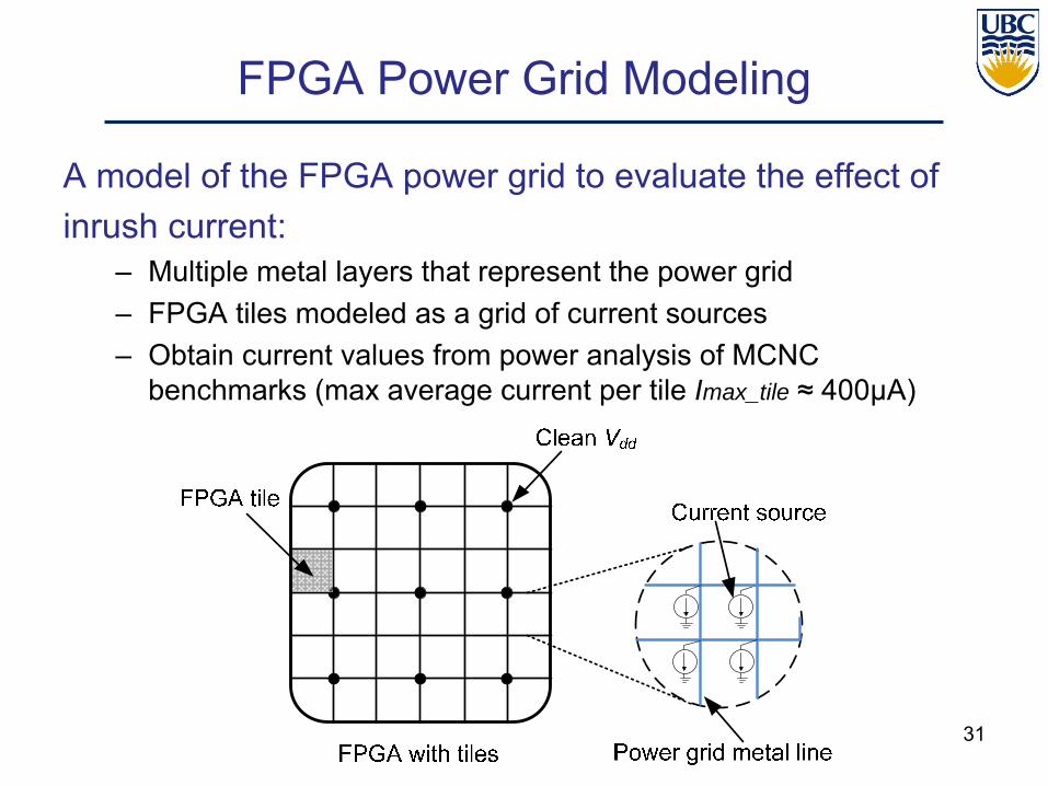
FPGA Power Grid Modeling
A model of the FPGA power grid to evaluate the effect ofinrush current:
– Multiple metal layers that represent the power grid– FPGA tiles modeled as a grid of current sources– Obtain current values from power analysis of MCNC
benchmarks (max average current per tile Imax_tile ≈ 400µA)

32
Effect of Inrush Current
Voltage drop due to inrush current in our FPGA architecture.
Voltage drop on power grid is larger than 100mV!
Finer granularity
Volta
ge D
rop
(mV)
33
What are the possible solutions for our power-gated FPGA?
34
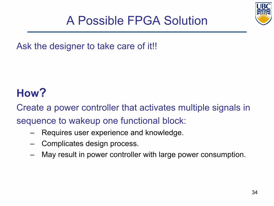
A Possible FPGA Solution
Ask the designer to take care of it!!
How?Create a power controller that activates multiple signals insequence to wakeup one functional block:
– Requires user experience and knowledge.– Complicates design process.– May result in power controller with large power consumption.
35
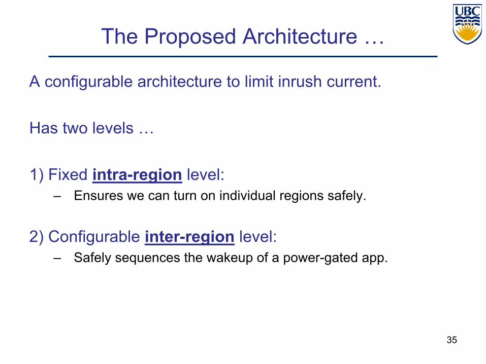
The Proposed Architecture …
A configurable architecture to limit inrush current.
Has two levels …
1) Fixed intra-region level:– Ensures we can turn on individual regions safely.
2) Configurable inter-region level:– Safely sequences the wakeup of a power-gated app.
36
Fixed Intra-region Architecture

37
Intra-region Architecture
Use parallel sleeptransistors (STs) andsequence wakeupusing fixed delayelements.
Sizes of STs and delay elements isbased on maximum allowed current.
A Tradeoff exists between area overhead of intra-region level and power grid metal area.

38
Configurable Inter-region Architecture

39
Inter-region Architecture
Intra-region level should solve the problem (theoretically!)
However …In practice more current might be drawn due to:
– Switching of unrelated signals in routing.– Switching of inputs to logic clusters partially turned on.
Which is application specific!
Instead of turning on a complete power-gated applicationat once, turn on one power gating region at a time.

40
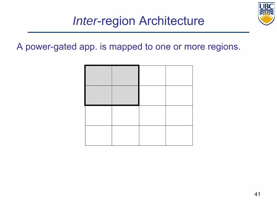
FPGA chip with power gating regions.
Inter-region Architecture
Power gating region in FPGA
41
Inter-region Architecture
A power-gated app. is mapped to one or more regions.
42
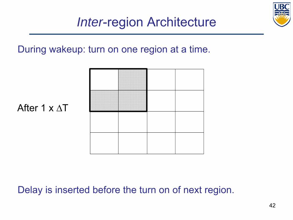
Inter-region Architecture
During wakeup: turn on one region at a time.
Delay is inserted before the turn on of next region.
After 1 x ∆T

43
Inter-region Architecture
During wakeup: turn on one region at a time.
Delay is inserted before the turn on of next region.
After 2 x ∆T

44
Inter-region Architecture
During wakeup: turn on one region at a time.
Delay is inserted before the turn on of next region.
After 3 x ∆T

45
Inter-region Architecture
During wakeup: turn on one region at a time.
After 4 x ∆T

46
Inter-region Architecture
We need to insert delays between the turn-on of regions.
However … we don’t know:– the shape, size, and location of a power-gated app. on FPGA.– how many delays are required before turning on a region.
Use programmable delay elements (PDEs).

47
Inter-region Architecture
PDE size (number of inputs) ≡ the largest power-gatedapp. that can be turned on using one control signal.
MU
X
Power Gating Region
VDD
01
SLEEP
∆T1∆Tn-1
Virtual VDDST1ST2STn
From bordering routing channels
PDE
Inter-region
Programmable delay element (PDE)

48
Inter-region Architecture
C1 C1
C1 C1

49
Inter-region Architecture
C1 C1
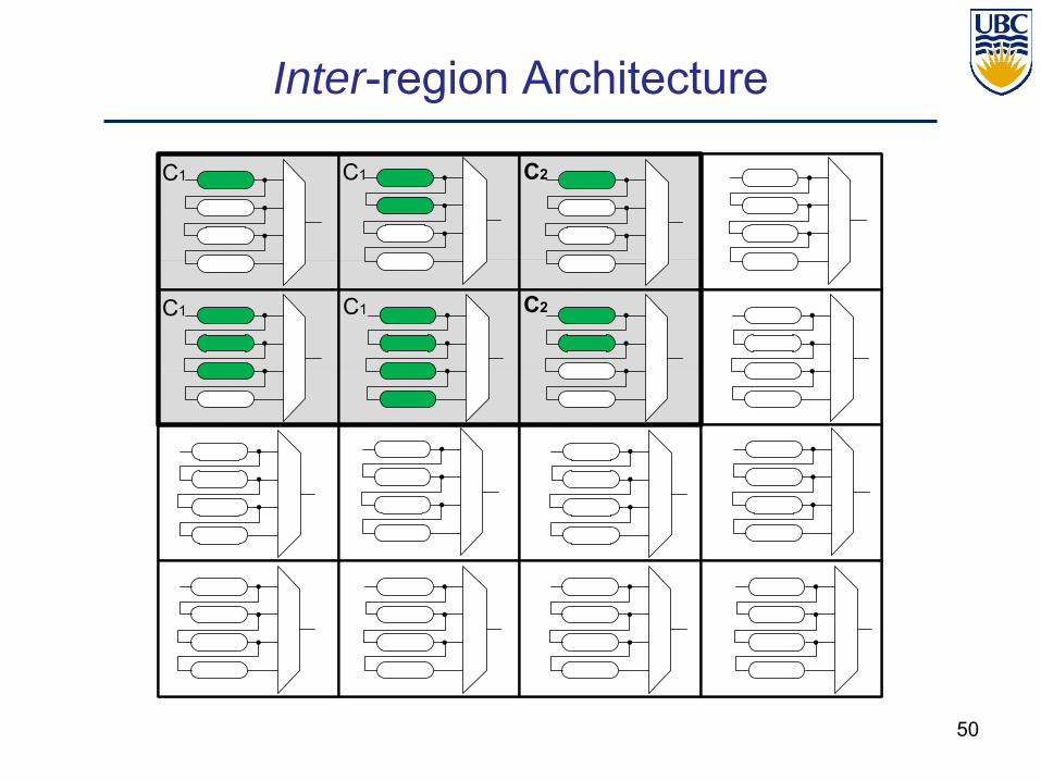
50
Inter-region Architecture
C1 C1
C1 C1
C2
C2

51
Results: Inrush Current Handling
Settings:– Region size = 4x4– Typical power grid (not oversized)– Worst case temperature– PDE size (# of regions controlled using one signal): 50
Leakage power savings (compared to ungated):– With inrush handling: 91%– Without inrush handling: 97%
Area overhead (compared to ungated):– Less than 2.2%

52
Outline
• Power gating architecture• Complications: wakeup current• System-level evaluation • Current work• Other issues

53
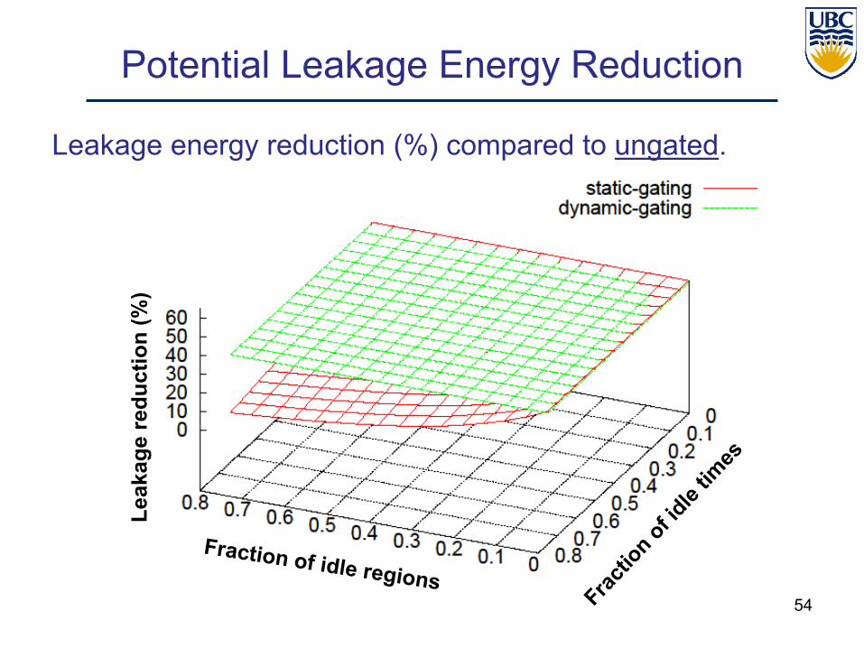
Potential Leakage Energy Reduction
Use a model that relates:– Number and size of idle regions in application– Proportion of the time idle regions can be turned off– Size of the “power controller”– Potential slowdown of application
… to the energy savings of the architecture
54
Potential Leakage Energy Reduction
Leakage energy reduction (%) compared to ungated.
Fraction of idle regionsFrac
tion of id
le tim
es
Leak
age
redu
ctio
n (%
)

55
Conditions to Achieve Energy Savings
To achieve savings: Esleep < Eidle
Use a model to find the minimum idle time required in order to achieve energy savings when in sleep mode.
For clma (775 tiles ≡ PDE size 49), Tidle ≈ 900 ns.– Equivalent to 450 cycles on 500 MHz clock!
56
Outline
• Power gating architecture• Complications: wakeup current• System-level evaluation• Current work • Other issues
57
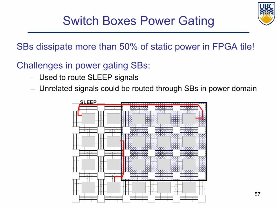
Switch Boxes Power Gating
SBs dissipate more than 50% of static power in FPGA tile!
Challenges in power gating SBs:– Used to route SLEEP signals– Unrelated signals could be routed through SBs in power domain
SLEEP

58
Switch Boxes Power Gating
Solution: partial power gating for SBs– Allows off mode for SBs inside power domain– Allows partial off mode for shared SBs
SLEEP

59
Outline
• Power gating architecture• Complications: wakeup current• System-level evaluation• Current work• Other issues
60
Applications Mapping to Architecture
Mapping applications (high level):– Automatic detection for power domains in app– Automatic generation for power controller
What about verification?
61
Evaluation and Benchmarks
What we have used so far:– HSPICE circuit models and simulations– Architecture parameter sweep– Application model to find potential savings, min Tidle, etc.
What we really need:– Real applications with power domains– More advanced power model– A way to map applications to architecture

62
Summary
Summary of dynamically-controlled power gating FPGA:1. Enables turning off unused logic at config time – static power2. Enables turning off idle logic at runtime – static power3. Control could come from off or on chip (from soft logic)4. Programmable inrush current handling5. Routing architecture is not changed (until now)
Challenges:1. Area overhead – small though2. Performance degradation – we assume 10% for now3. Mapping applications to architecture – automated?