an 777: data word alignment calibration with multiple ... · 1 an 777: data word alignment...
TRANSCRIPT

AN 777: Data Word AlignmentCalibration With Multiple Intel FPGAPHYLite for Parallel Interfaces IPCores
SubscribeSend Feedback
AN-777 | 2018.01.12Latest document on the web: PDF | HTML
Contents
1 AN 777: Data Word Alignment Calibration With Multiple Intel FPGA PHYLite forParallel Interfaces IP Cores.......................................................................................31.1 Features................................................................................................................31.2 Hardware and Software Requirements....................................................................... 31.3 Compiling the Reference Design............................................................................... 31.4 Hardware Setup..................................................................................................... 81.5 Generating Executable and Linking Format (.elf) Programming File................................91.6 Running the Hardware Reference Design..................................................................121.7 Results................................................................................................................13
1.7.1 Random Data Transfer Result......................................................................131.7.2 Dynamic Calibration Result.........................................................................14
1.8 Reference Design Architecture................................................................................ 161.8.1 Functional Description............................................................................... 161.8.2 Data Word Alignment Algorithm.................................................................. 181.8.3 Timing Analysis Guidelines......................................................................... 20
1.9 Document Revision History for AN 777: Data Word Alignment Calibration WithMultiple Intel FPGA PHYLite for Parallel Interfaces IP Cores..................................... 23
Contents
AN 777: Data Word Alignment Calibration With Multiple Intel FPGA PHYLite for Parallel Interfaces IP Cores2
1 AN 777: Data Word Alignment Calibration With MultipleIntel FPGA PHYLite for Parallel Interfaces IP Cores
This application note describes a design example which demonstrates data alignmentcalibration using multiple Intel FPGA PHYLite for Parallel Interfaces IP cores.
1.1 Features
• Data word alignment using Intel FPGA PHYLite for Parallel Interfaces dynamicconfiguration feature
• Using Nios II processor as configuration controller
• Provides I/O timing constraint guidelines between two Intel FPGA PHYLite forParallel Interfaces instances
• Supports hardware testing
1.2 Hardware and Software Requirements
Hardware Requirements
• Intel® Intel Arria® 10 FPGA Development Kit (Device OPN:10AX115S3F45E2SGE3)
• Loopback FPGA mezzanine (FMC) daughter card
• Intel FPGA Intel FPGA Download Cable
Software Requirements
• Intel Intel Quartus® Prime Design Suite version 16.0
• Arria10_Phylite_Word_Alignment_Calibration.qar file.
1.3 Compiling the Reference Design
1. Follow the guidelines in Getting Started with the Design Store to download andinstall the reference design files.
2. Open the reference design .qpf file after successfully installing the designtemplates.
3. In the Intel Quartus Prime software, open dut_INPUT.qsys anddut_OUTPUT.qsys files. Make sure the Intel FPGA PHYLite IP core has the sameconfigurations shown below:
AN-777 | 2018.01.12
Intel Corporation. All rights reserved. Intel, the Intel logo, Altera, Arria, Cyclone, Enpirion, MAX, Nios, Quartusand Stratix words and logos are trademarks of Intel Corporation or its subsidiaries in the U.S. and/or othercountries. Intel warrants performance of its FPGA and semiconductor products to current specifications inaccordance with Intel's standard warranty, but reserves the right to make changes to any products and servicesat any time without notice. Intel assumes no responsibility or liability arising out of the application or use of anyinformation, product, or service described herein except as expressly agreed to in writing by Intel. Intelcustomers are advised to obtain the latest version of device specifications before relying on any publishedinformation and before placing orders for products or services.*Other names and brands may be claimed as the property of others.
ISO9001:2008Registered
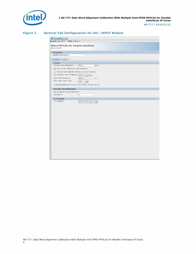
Figure 1. General Tab Configuration for dut_INPUT Module
1 AN 777: Data Word Alignment Calibration With Multiple Intel FPGA PHYLite for ParallelInterfaces IP Cores
AN-777 | 2018.01.12
AN 777: Data Word Alignment Calibration With Multiple Intel FPGA PHYLite for Parallel Interfaces IP Cores4

Figure 2. Group 0 Tab Configuration for dut_INPUT Module
1 AN 777: Data Word Alignment Calibration With Multiple Intel FPGA PHYLite for ParallelInterfaces IP Cores
AN-777 | 2018.01.12
AN 777: Data Word Alignment Calibration With Multiple Intel FPGA PHYLite for Parallel Interfaces IP Cores5

Figure 3. General Tab Configuration for dut_OUTPUT Module
1 AN 777: Data Word Alignment Calibration With Multiple Intel FPGA PHYLite for ParallelInterfaces IP Cores
AN-777 | 2018.01.12
AN 777: Data Word Alignment Calibration With Multiple Intel FPGA PHYLite for Parallel Interfaces IP Cores6

Figure 4. Group 0 Tab Configuration for dut_OUTPUT Module
4. In Intel Quartus Prime software, click on Assignments ➤ Settings ➤ TimeQuestTiming Analyzer.
5. In the Tcl Script File name, type in phylite_interface_constraints.tcland select Run default timing analysis before running customer script.
1 AN 777: Data Word Alignment Calibration With Multiple Intel FPGA PHYLite for ParallelInterfaces IP Cores
AN-777 | 2018.01.12
AN 777: Data Word Alignment Calibration With Multiple Intel FPGA PHYLite for Parallel Interfaces IP Cores7
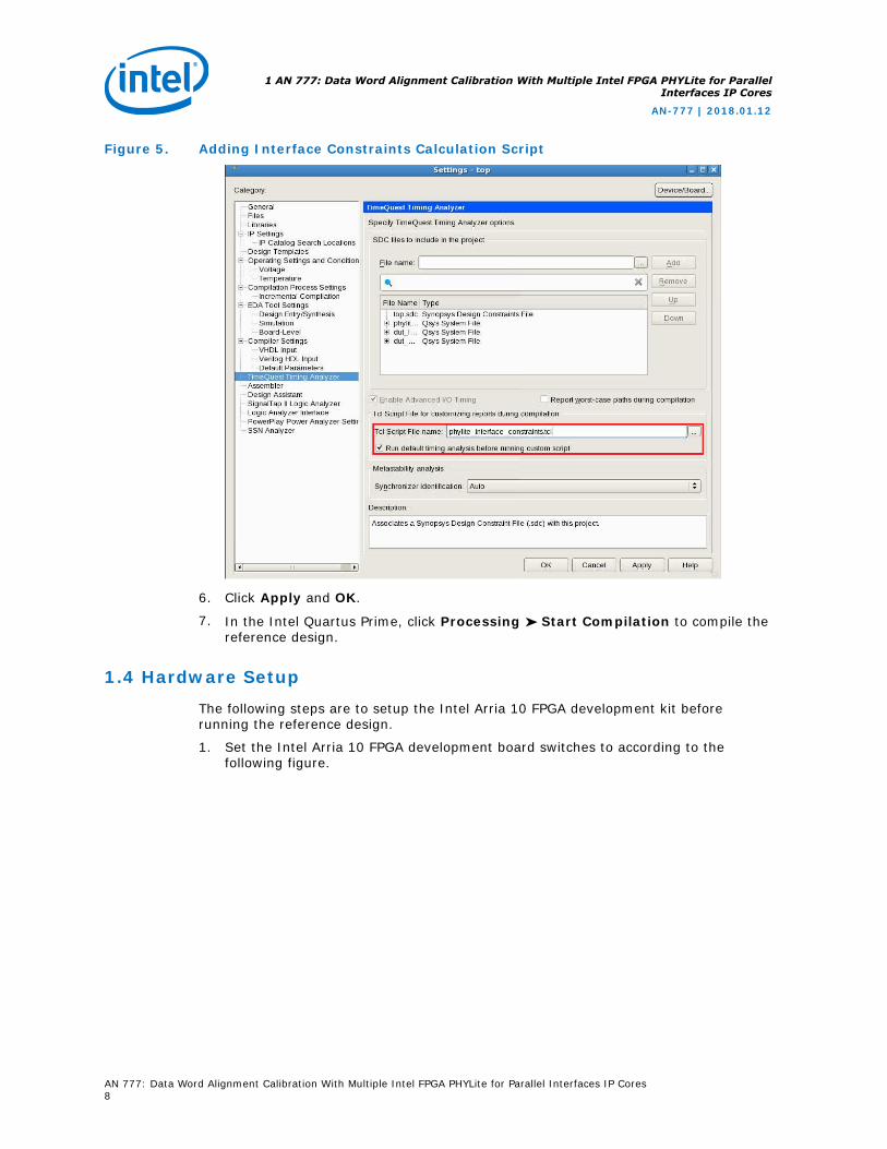
Figure 5. Adding Interface Constraints Calculation Script
6. Click Apply and OK.
7. In the Intel Quartus Prime, click Processing ➤ Start Compilation to compile thereference design.
1.4 Hardware Setup
The following steps are to setup the Intel Arria 10 FPGA development kit beforerunning the reference design.
1. Set the Intel Arria 10 FPGA development board switches to according to thefollowing figure.
1 AN 777: Data Word Alignment Calibration With Multiple Intel FPGA PHYLite for ParallelInterfaces IP Cores
AN-777 | 2018.01.12
AN 777: Data Word Alignment Calibration With Multiple Intel FPGA PHYLite for Parallel Interfaces IP Cores8

Figure 6. Intel Arria 10 FPGA Development Board Switch Settings
2. Connect the loopback FPGA mezzanine (FMC) daughter card on the FMC loopbackPort B.
Figure 7. Connection for Loopback FPGA Mezzanine (FMC) Daughter Card
3. Connect the Intel FPGA Download Cable to the Intel Arria 10 FPGA developmentkit and your host machine.
4. Click Tools -> Programmer to program the <project directory> /master_image/top.sof file into the Arria 10 FPGA development board.
1.5 Generating Executable and Linking Format (.elf) ProgrammingFile
Follow the steps below to generate an executable and linking format (.elf)programming file. These steps are necessary if you would like to modify thephylite_dynamic_reconfiguration.c,phylite_dynamic_reconfiguration.h and hello_world.c files.
1. In the Intel Quartus Prime software version 16.0 select Tools ➤ Nios IISoftware Build Tools for Eclipse .
1 AN 777: Data Word Alignment Calibration With Multiple Intel FPGA PHYLite for ParallelInterfaces IP Cores
AN-777 | 2018.01.12
AN 777: Data Word Alignment Calibration With Multiple Intel FPGA PHYLite for Parallel Interfaces IP Cores9

Figure 8. Nios II Software Build Tools for Eclipse
2. Create a new workspace when the Select a workspace window prompt appears.
1 AN 777: Data Word Alignment Calibration With Multiple Intel FPGA PHYLite for ParallelInterfaces IP Cores
AN-777 | 2018.01.12
AN 777: Data Word Alignment Calibration With Multiple Intel FPGA PHYLite for Parallel Interfaces IP Cores10
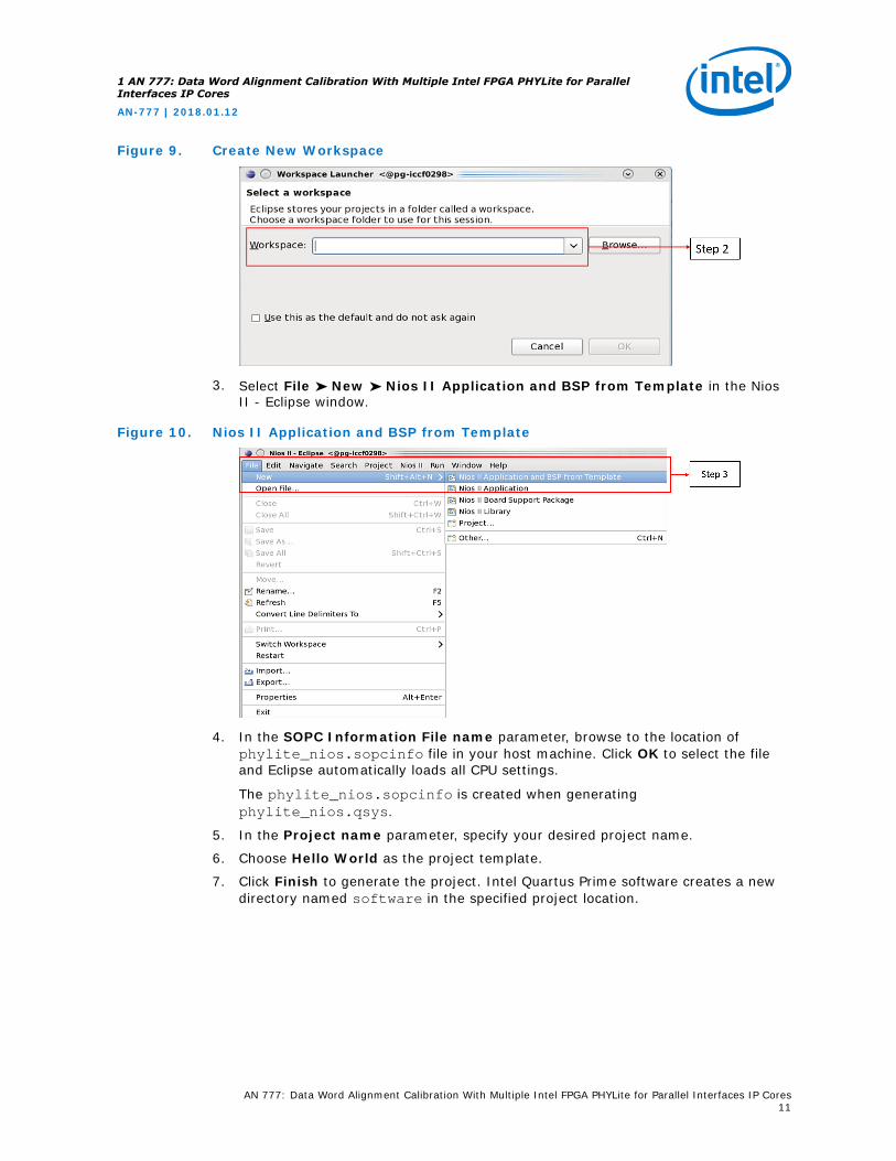
Figure 9. Create New Workspace
3. Select File ➤ New ➤ Nios II Application and BSP from Template in the NiosII - Eclipse window.
Figure 10. Nios II Application and BSP from Template
4. In the SOPC Information File name parameter, browse to the location ofphylite_nios.sopcinfo file in your host machine. Click OK to select the fileand Eclipse automatically loads all CPU settings.
The phylite_nios.sopcinfo is created when generatingphylite_nios.qsys.
5. In the Project name parameter, specify your desired project name.
6. Choose Hello World as the project template.
7. Click Finish to generate the project. Intel Quartus Prime software creates a newdirectory named software in the specified project location.
1 AN 777: Data Word Alignment Calibration With Multiple Intel FPGA PHYLite for ParallelInterfaces IP Cores
AN-777 | 2018.01.12
AN 777: Data Word Alignment Calibration With Multiple Intel FPGA PHYLite for Parallel Interfaces IP Cores11

Figure 11. Nios II Application and BSP from Template Settings
8. Replace the following files from <project directory>/software referencedesign with the files located in your new software directory.
• hello_world.c
• phylite_dynamic_reconfiguration.c
• phylite_dynamic_reconfiguration.h
9. In the Nios II - Eclipse window, press F5 to refresh the window and reload the newfiles into the project.
10. Click Project ➤ Build Project.
11. Make sure the <project_name>.elf file is generated in the new <projectdirectory>/software/<project_name>/ directory.
1.6 Running the Hardware Reference Design
These steps are guidelines to run the dynamic calibration and begin the data transferfor the reference design.Remove all other connected device in the programming device list during JTAGconnection setup in Linux operating system.
1. Open two Nios II Command Shell prompts on your host machine:
a. In Windows operating system, go to Start ➤ Programs ➤ Altera ➤ Nios IIEDS and click on Nios II Command Shell (command prompt A).
1 AN 777: Data Word Alignment Calibration With Multiple Intel FPGA PHYLite for ParallelInterfaces IP Cores
AN-777 | 2018.01.12
AN 777: Data Word Alignment Calibration With Multiple Intel FPGA PHYLite for Parallel Interfaces IP Cores12

b. In Linux operating system, go to <Quartus software installationdirectory>\linux64\nios2ed directory and runnios2_command_shell.sh to launch command prompt A.
c. Repeat the above step to launch second command prompt (command promptB).
Command prompt A is to display the dynamic calibration result. Command promptB is used to run Nios II commands.
2. In the command prompt A , use the following command to run the Nios II terminalapplication for result printouts.
nios2-terminal
3. In command prompt B, go to the project top directory.
cd <project directory>
4. Run the issp.tcl script once to reset the system and clean up the instructionmemory in the Nios II soft processor.
quartus_stp -t issp.tcl top.qpf 1 0
5. In command prompt B, download the executable (<project_name>.elf) fileinto the FPGA and start the dynamic calibration process with the followingcommand:
nios2-download -r -g software/<project_name>/<projct_name>.elf
You may observe the passing dynamic calibration result displayed in commandprompt A.
6. When the Nios II instruction memory is cleaned and calibration is done, run thefollowing command in command prompt B to reset the system, start the randomdata transfer and capture internal signals.
quartus_stp -t issp.tcl top.qpf 1 1 1
Note: You will see sent and received data displayed in command prompt B afterrunning the command.
1.7 Results
The hardware reference design provides:
• Dynamic calibration result
• Random data transfer result
1.7.1 Random Data Transfer Result
Synopsis:
The result log from the random data transfer process displays the following:
• The number of words being transferred
• The sent data value
• The expected data value
• The received data value
• The passing/failing status of the test
1 AN 777: Data Word Alignment Calibration With Multiple Intel FPGA PHYLite for ParallelInterfaces IP Cores
AN-777 | 2018.01.12
AN 777: Data Word Alignment Calibration With Multiple Intel FPGA PHYLite for Parallel Interfaces IP Cores13

Figure 12. Example of Random Data Transfer Result Log
1.7.2 Dynamic Calibration Result
The following screen capture shows the dynamic calibration result of the hardwarereference design.
1 AN 777: Data Word Alignment Calibration With Multiple Intel FPGA PHYLite for ParallelInterfaces IP Cores
AN-777 | 2018.01.12
AN 777: Data Word Alignment Calibration With Multiple Intel FPGA PHYLite for Parallel Interfaces IP Cores14
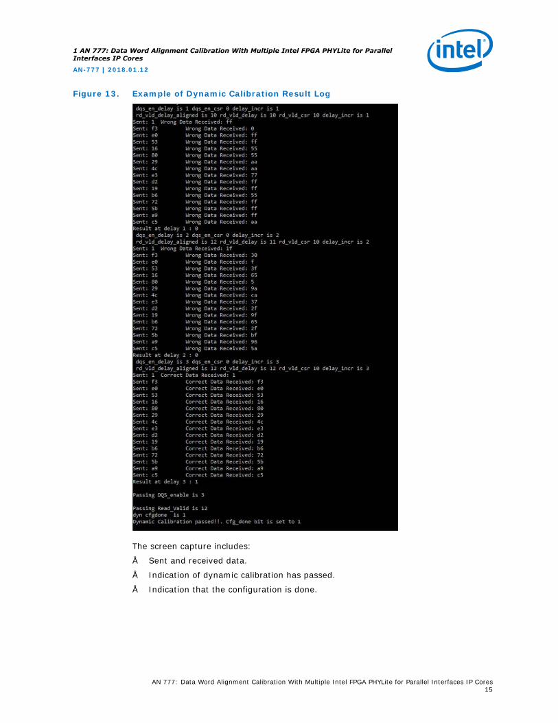
Figure 13. Example of Dynamic Calibration Result Log
The screen capture includes:
• Sent and received data.
• Indication of dynamic calibration has passed.
• Indication that the configuration is done.
1 AN 777: Data Word Alignment Calibration With Multiple Intel FPGA PHYLite for ParallelInterfaces IP Cores
AN-777 | 2018.01.12
AN 777: Data Word Alignment Calibration With Multiple Intel FPGA PHYLite for Parallel Interfaces IP Cores15

1.8 Reference Design Architecture
Figure 14. Reference Design Block Diagram
Traffic Generator
NIOS II ProcessorAvalon Bus Avalon Bus
Avalon Controller IOAUX
Avalon Bus
dut_OUTPUT(Intel FPGA PHYLite for Parallel Interfaces IP Core)
dut_INPUT(Intel FPGA PHYLite for Parallel Interfaces IP Core)
Data Write
Data Read
Data
Strobe
dutATSO_DYN_CFG_CTRL
PLL
core_clk_out
core_clk_out
core_clk_out
ref_clk
ref_clk
The reference design contains:
• dut_INPUT module
• dut_OUTPUT module
• PLL module
• Avalon controller
• ATSO_DYN_CFG_CTRL module with Nios II processor
• Traffic generator
Related Links
Altera PHYLite for Parallel Interfaces IP Core User Guide
1.8.1 Functional Description
PLL module
This module takes the input from Si570 Programmable Oscillator and providesreference clock to the internal PLL modules in each of the Intel FPGA PHYLite forParallel Interfaces IP cores.
dut_OUTPUT Module
This Intel FPGA PHYLite for Parallel Interfaces IP core transfers data fromATSO_DYN_CFG_CTRL or traffic generator module to dut_INPUT module. Duringconfiguration and calibration mode, this module takes data fromATSO_DYN_CFG_CTRL module and send to dut_INPUT module. In normal operatingmode, this module takes data from traffic generator and sends to dut_INPUT module.
1 AN 777: Data Word Alignment Calibration With Multiple Intel FPGA PHYLite for ParallelInterfaces IP Cores
AN-777 | 2018.01.12
AN 777: Data Word Alignment Calibration With Multiple Intel FPGA PHYLite for Parallel Interfaces IP Cores16

dut_INPUT Module
This Intel FPGA PHYLite for Parallel Interfaces IP core receives data from dut_OUTPUTmodule. This module sends the received data to ATSO_DYN_CFG_CTRL module duringconfiguration and calibration mode, and to traffic generator during normal operatingmode for data verification.
Avalon Controller
The Avalon controller is responsible to perform address translation to retrieve thephysical address of the strobe and data pins and sends reconfiguration commands todut_OUTPUT module.
ATSO_DYN_CFG_CTRL with Nios II Processor Module
This module consist of Nios II processor and five parallel I/O modules. This is acentralized controller to perform and manage dut_OUTPUT configuration. It also issuescontrol signals to the Avalon controller and verify data from dut_INPUT duringcalibration mode.
Table 1. Parallel I/O Modules - Function and Address Map
Parallel I/O Module Address Map Description
phy_write_data 0x20 Sends calibration test data todut_OUTPUT module.
phy_write_ctrl 0x30 Asserts rdata_en signal duringcalibration mode.
phy_read_data 0x40 Receives data from dut_INPUT modulefor comparison against test data.
phy_read_status 0x50 Receives rdata_valid signal fromdut_INPUT module.
cal_mode 0x60 Asserts cfg_done signal to exitcalibration mode and activates trafficgenerator module for data transfer fornormal operating mode.
Traffic Generator Module
Traffic Generator module is responsible for transmitting data to dut_OUTPUT andreceiving data from dut_INPUT during normal operating mode. The module usesLinear Feedback Shift Register (LFSR) to generate random data for transmission.Traffic generator performs data comparison to the received data to ensure the strobeenable delay setting is configured correctly.
Related Links
• Altera PHYLite for Parallel Interfaces IP Core User Guide
• How do I compensate for the jitter of PLL cascading or non-dedicated clock pathfor Arria 10 PLL reference clock?
1 AN 777: Data Word Alignment Calibration With Multiple Intel FPGA PHYLite for ParallelInterfaces IP Cores
AN-777 | 2018.01.12
AN 777: Data Word Alignment Calibration With Multiple Intel FPGA PHYLite for Parallel Interfaces IP Cores17
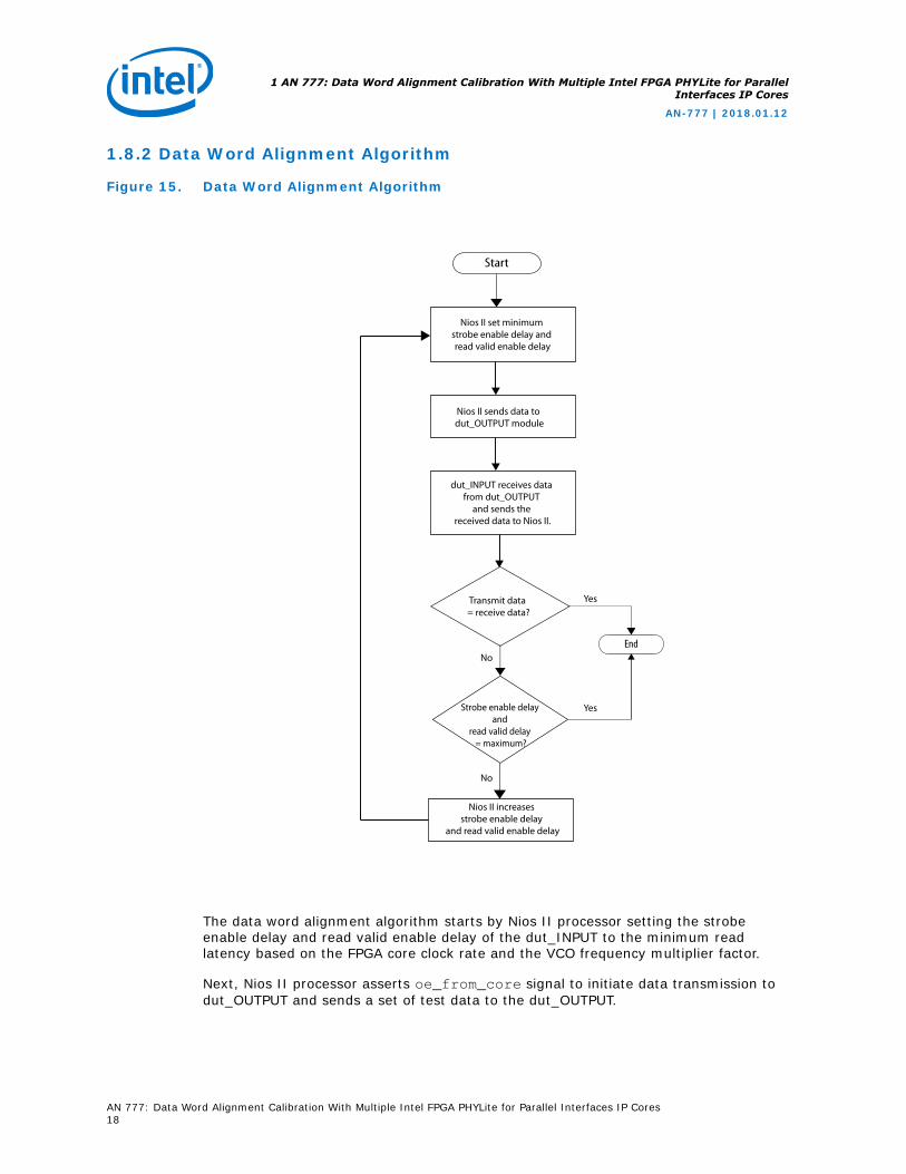
1.8.2 Data Word Alignment Algorithm
Figure 15. Data Word Alignment Algorithm
Start
Nios II set minimum strobe enable delay and read valid enable delay
Nios II sends data to dut_OUTPUT module
End
dut_INPUT receives data from dut_OUTPUT
and sends the received data to Nios II.
Yes
Transmit data = receive data?
Strobe enable delay and
read valid delay = maximum?
Yes
No
No
Nios II increases strobe enable delay
and read valid enable delay
The data word alignment algorithm starts by Nios II processor setting the strobeenable delay and read valid enable delay of the dut_INPUT to the minimum readlatency based on the FPGA core clock rate and the VCO frequency multiplier factor.
Next, Nios II processor asserts oe_from_core signal to initiate data transmission todut_OUTPUT and sends a set of test data to the dut_OUTPUT.
1 AN 777: Data Word Alignment Calibration With Multiple Intel FPGA PHYLite for ParallelInterfaces IP Cores
AN-777 | 2018.01.12
AN 777: Data Word Alignment Calibration With Multiple Intel FPGA PHYLite for Parallel Interfaces IP Cores18
The dut_OUTPUT transmit the test data to the dut_INPUT. Thercfg_data_from_core signals show the data value transmitted from dut_OUTPUT.
Next, the dut_INPUT sends the test data to Nios II processor for data verification. NiosII asserts recfg_rdata_en signal to dut_INPUT to capture the data transmitted fromdut_OUTPUT. The dut_INPUT module asserts recfg_rdata_valid signal to indicatesthe received data in the dut_INPUT read FIFO is valid. If the received test data doesnot match the expected data, Nios II processor increases the strobe enable delay andread valid enable delay of the dut_INPUT module, and repeats the process of sendingtest data to dut_OUTPUT and verify the received data from dut_INPUT.
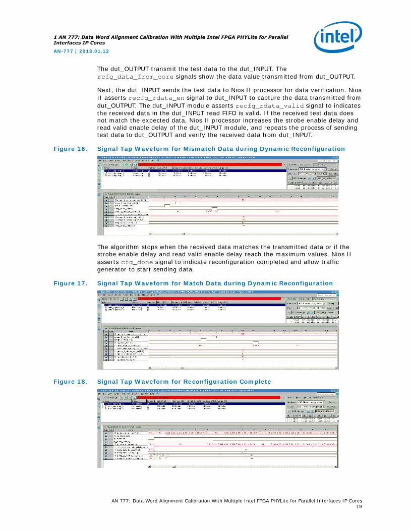
Figure 16. Signal Tap Waveform for Mismatch Data during Dynamic Reconfiguration
The algorithm stops when the received data matches the transmitted data or if thestrobe enable delay and read valid enable delay reach the maximum values. Nios IIasserts cfg_done signal to indicate reconfiguration completed and allow trafficgenerator to start sending data.
Figure 17. Signal Tap Waveform for Match Data during Dynamic Reconfiguration
Figure 18. Signal Tap Waveform for Reconfiguration Complete
1 AN 777: Data Word Alignment Calibration With Multiple Intel FPGA PHYLite for ParallelInterfaces IP Cores
AN-777 | 2018.01.12
AN 777: Data Word Alignment Calibration With Multiple Intel FPGA PHYLite for Parallel Interfaces IP Cores19

Related Links
Altera PHYLite for Parallel Interfaces IP Core User Guide
1.8.3 Timing Analysis Guidelines
The reference design uses the following timing analysis flow to obtain the accuratevalue for Input Strobe Setup Delay, Input Strobe Hold Delay Constraint,Output Strobe Setup Delay Constraint,, and Output Strobe Hold DelayConstraint to perform timing closure for both output and input interfaces.
Figure 19. Timing Analysis Flow
Start
Set Output Strobe Setup Delay Constraint = 0 ns
Set Output Strobe Hold Delay Constraint = 0 ns
Add TcoMax and TcoMin to dut_INPUT module input delay through parameter editor
Set Input Strobe Setup Delay Constraint = 0 ns
Set Input Strobe Hold Delay Constraint = 0 ns
Compile design to calculate TcoMax and TcoMin for dut_INPUT module input delay constraints
Compile design and perform timing analysis for individual Altera PHYLite instances
End
1 AN 777: Data Word Alignment Calibration With Multiple Intel FPGA PHYLite for ParallelInterfaces IP Cores
AN-777 | 2018.01.12
AN 777: Data Word Alignment Calibration With Multiple Intel FPGA PHYLite for Parallel Interfaces IP Cores20

It is crucial to set the Input Strobe Setup Delay, Input Strobe Hold DelayConstraint, Output Strobe Setup Delay Constraint, and Output Strobe HoldDelay Constraint for both dut_INPUT and dut_OUTPUT module to 0 initially toeliminate unnecessary interface constraints. Thephylite_interface_constraints.tcl script then automatically calculates theTcoMax and TcoMin values for input interface delay constraints and Tsu and Th valuesfor output interface delay constraints.
The TimeQuest Analyzer generates a report based on the calculations performed bythe script.
Figure 20. PHYLite Interface Constraints Report
Input Interface Delay Constraints
Use the TcoMax value to calculate the Input Strobe Setup Delay Constraint andTcoMin value to calculate the Input Strobe Hold Delay Constraint. The inputinterface delay constraints must include board skew to perform accurate timinganalysis.
Input Strobe Setup Delay Constraint = TcoMax + board skew
Input Strobe Hold Delay Constraint = TcoMin + board skew
1 AN 777: Data Word Alignment Calibration With Multiple Intel FPGA PHYLite for ParallelInterfaces IP Cores
AN-777 | 2018.01.12
AN 777: Data Word Alignment Calibration With Multiple Intel FPGA PHYLite for Parallel Interfaces IP Cores21

Update the new Input Strobe Setup Delay Constraint and Input Strobe HoldDelay Constraint values to the dut_INPUT module and re-compile the design.
Figure 21. Calculated Input Interface Delay Constraints
Output Interface Delay Constraints
Use the Tsu value to calcuate the Output Strobe Setup Delay Constraint and Thvalue to calculate Output Strobe Hold Delay Constraint. The output interface delayconstraints must include board skew to perform accurate timing analysis.
Output Strobe Setup Delay Constraint = Tsu + board skew
Output Strobe Hold Delay Constraint = Th - board skew
Update the new Output Strobe Setup Delay Constraint and Output Strobe HoldDelay Constraint values to the dut_OUTPUT module and re-compile the design.
1 AN 777: Data Word Alignment Calibration With Multiple Intel FPGA PHYLite for ParallelInterfaces IP Cores
AN-777 | 2018.01.12
AN 777: Data Word Alignment Calibration With Multiple Intel FPGA PHYLite for Parallel Interfaces IP Cores22

Figure 22. Calculated Output Interface Delay Constraints
1.9 Document Revision History for AN 777: Data Word AlignmentCalibration With Multiple Intel FPGA PHYLite for Parallel InterfacesIP Cores
Date Version Changes
January 2018 2018.01.12 • Updated Reference Design Block Diagram.• Updated PLL Module description.
May 2017 2017.05.08 Rebranded as Intel.
December 2016 2016.12.09 Initial release.
1 AN 777: Data Word Alignment Calibration With Multiple Intel FPGA PHYLite for ParallelInterfaces IP Cores
AN-777 | 2018.01.12
AN 777: Data Word Alignment Calibration With Multiple Intel FPGA PHYLite for Parallel Interfaces IP Cores23