afe8406 system evaluation kit and - pudn.comread.pudn.com/downloads97/ebook/398931/afe8406 system...
TRANSCRIPT
AFE8406 System Evaluation Kit andGC Studio Reference
User's Guide
May 2006
SLWU034

AFE8406 System Evaluation Kit and GCStudio Reference
User's Guide
Literature Number: SLWU034
May 2006

Contents
1 AFE8406 System Evaluation Kit Overview ..................................................................... 51.1 AFE8406 System Evaluation Kit .................................................................................. 6
2 Installing the Software ................................................................................................ 72.1 TSW2100 SPI Software Installation .............................................................................. 7
2.2 GC Studio Software Installation................................................................................... 8
3 Setting up the System ................................................................................................. 93.1 Hardware Setup..................................................................................................... 9
3.2 Loading and Running a GC Studio Project .................................................................... 12
3.2.1 ADC Experiments: AFE8406_TESTBUS_EX Directory ............................................. 12
3.2.2 UMTS Experiment: AFE8406_UMTS_EX Directory ................................................. 12
3.2.3 CDMA2000 Experiment: AFE8406_CDMA2k_EX Directory........................................ 12
3.2.4 DDC AGC Experiment: AFE8406_AGC_EX Directory .............................................. 13
3.2.5 Receive-Input AGC Experiment: AFE8406_RAGC_EX Directory ................................. 13
3.3 Creating a New GC Studio Project.............................................................................. 15
4 Other Options in GC Studio ....................................................................................... 334.1 Saving the Output to a File....................................................................................... 33
4.2 Changing the Data Capture Size................................................................................ 34
4.3 Capturing the AFE8406 Test Bus Output ...................................................................... 36
5 AFE8406 Daughtercard Description ............................................................................ 415.1 AFE8406 Daughtercard Pin Description ....................................................................... 41
5.2 AFE8406 Daughtercard Jumpers ............................................................................... 43
5.3 AFE8406 Daughtercard Power Supplies....................................................................... 43
5.4 AFE8406 Daughtercard Clock Configurations................................................................. 43
6 Physical Description ................................................................................................. 456.1 PCB Layout ........................................................................................................ 45
6.2 Parts List ........................................................................................................... 52
7 AFE8406 Daughtercard Schematics ............................................................................ 55
SLWU034–May 2006 Contents 3Submit Documentation Feedback

List of Figures
1-1 Kit Contents................................................................................................................... 63-1 System Setup ............................................................................................................... 103-2 Typical Setup ............................................................................................................... 113-3 TSW2100 SPI Software Screen.......................................................................................... 126-1 Top Layer 1 ................................................................................................................. 456-2 Ground Plane Layer 2 ..................................................................................................... 466-3 Signal Layer 3 .............................................................................................................. 476-4 Signal Layer 4 .............................................................................................................. 486-5 Power Plane Layer 5....................................................................................................... 496-6 Signal Layer 6 .............................................................................................................. 506-7 Ground Plane Layer 7 ..................................................................................................... 516-8 Bottom Layer 8 ............................................................................................................. 52
List of Tables
3-1 Clock Requirements ......................................................................................................... 93-2 SMA Cable Connections .................................................................................................. 103-3 Default Jumper Settings ................................................................................................... 105-1 Memory Input Bus—36 Data Inputs Used to Stimulate the AFE8406 Inputs ...................................... 415-2 Memory Output Bus—36 Data Outputs From Selected AFE8406 Outputs Captured by the GC101 ........... 425-3 Clock ......................................................................................................................... 425-4 Microprocessor Control Bus—Bus to Program the Internal Registers .............................................. 425-5 JTAG ......................................................................................................................... 425-6 Power and Ground ......................................................................................................... 426-1 AFE8406 Daughtercard Bill of Materials (BOM) ....................................................................... 52
4 List of Figures SLWU034–May 2006Submit Documentation Feedback

C001
Chapter 1SLWU034–May 2006
AFE8406 System Evaluation Kit Overview
The AFE8406 is a multichannel communications signal processor that providesanalog-to-digital conversion and digital downconversion optimized for cellular basetransceiver systems. The device supports UMTS, CDMA-1X and TD-SCDMAair-interface cellular standards.
The AFE8406 provides up to 8 UMTS digital downconverter channels (DDC), 16 CDMADDCs, or 16 TD-SCDMA DDCs. The DDC channels are independent and operatesimultaneously. At the AFE8406 inputs, there are four input ports: two are hardwired tointernal 14-bit analog-to-digital converters and two are 16-bit digital inputs. Each DDCchannel can be programmed to accept data from any one of the four input ports.
The AFE8406 system evaluation kit is a set of hardware and software tools designed toease the AFE8406 evaluation. This guide provides a step-by-step description on how toset up the AFE8406 system solution.
Windows, Windows XP are trademarks of Microsoft Corporation.All trademarks are the property of their respective owners.
SLWU034–May 2006 AFE8406 System Evaluation Kit Overview 5Submit Documentation Feedback

www.ti.com
1.1 AFE8406 System Evaluation Kit
M0050-01
SMA cables
5-V power supply for TSW2100
GC101 motherboard
5-V power supply for GC101
AFE8406 daughtercard
TSW2100 clock solution EVM
Parallel port cable Software CD
AFE8406 System Evaluation Kit
The AFE8406 system evaluation kit includes the items shown in Figure 1-1:
Figure 1-1. Kit Contents
The CD includes two software packages that must be installed before connecting the hardware:• TSW2100 SPI software – used to configure the TSW2100• GC Studio software – used to configure the GC101 and AFE8406 as well as to analyze the results
6 AFE8406 System Evaluation Kit Overview SLWU034–May 2006Submit Documentation Feedback

2.1 TSW2100 SPI Software Installation
C002
Chapter 2SLWU034–May 2006
Installing the Software
All necessary software to operate the serial interface is provided on the included CD.This section describes in detail how to install the required software packages.
The TSW2100 SPI is a GUI-based software that allows full control and programmability of the CDCM7005(core device of the TSW2100). Load the software as follows:
1. Insert the CD into the computer to be used to operate the serial interface.2. Open the TSW2100_Installv1p0 folder.3. Double-click on the file called setup.exe.4. The Installation Wizard opens. Follow the on-screen instructions.5. After the installation is complete, you can access the program from the programs list on the Start
menu.6. On starting the program, the following screen should be present:
SLWU034–May 2006 Installing the Software 7Submit Documentation Feedback

www.ti.com
2.2 GC Studio Software Installation
C003
GC Studio Software Installation
For more information on the various parameters shown on the GUI, see the CDCM7005 product page:http://focus.ti.com/docs/prod/folders/print/cdcm7005.html.
The GC Studio software program, along with the GC101 motherboard, provides a framework to evaluatethe AFE8406. The primary uses of the GC101 EVM are to program the AFE8406, to provide a stream ofstimulus information, and to capture the response information for processing by the computer. The GCStudio software controls the GC101 EVM, provides a stimulus image, and retrieves and processes theresponse image. Several GC Studio projects for the AFE8406 are included in the installation. Theseprojects can be used as the starting point for creating new experiments.
The minimum requirements to install GC Studio are:• Host computer (PC) with BIOS supporting ECP mode for LPT1, running Windows™ 98 SP 2, Windows
ME, Windows 2000 SP 1, Windows XP™ Home or Windows XP Professional• Administrator group privileges
The steps to install GC Studio are as follows:
1. Insert the CD into the computer to be used to operate the serial interface.2. Double-click the file called GCStudio_Minimal_Setup_xx_xx_xxxxxx.exe, where xx_xx_xxxx
corresponds to the GC Studio version number.3. The installation wizard opens. Follow the on-screen instructions. This will load the main GC Studio
software.4. Double-click the file called AFE8406_projects_xxxxxx.exe, where xxxx corresponds to the AFE8406
project version number.5. The installation wizard opens. Follow the on-screen instructions and use the default settings. This will
load the AFE8406 projects in the proper directory to allow access by the GC Studio software.6. After the installation is complete, you can access the program from the programs list on the Start
menu.7. On starting the program, the following screen should be present:
8 Installing the Software SLWU034–May 2006Submit Documentation Feedback

3.1 Hardware Setup
Chapter 3SLWU034–May 2006
Setting up the System
The GC101 and AFE8406 daughtercard require three clocks when used for operation with an analog inputsignal. The clocks are described in Table 3-1.
Table 3-1. Clock Requirements
BOARD CONNECTOR DESCRIPTION
AFE8406 daughtercard CLKP (J6) AFE8406 ADC clock. On the AFE8406 daughtercard, thissignal is converted to a differential signal and routed toAFE8406 balls CLK(M/P)(A/B). It must be a low-jitter clockfor optimal performance.
AFE8406 daughtercard CLKM (J5) AFE8406 digital clock. Routed to AFE8406 ball RXCLK.
GC101 EXT CLK Digital clock input for GC101. Digital source and capturerate.
When the AFE8406 FIFO is enabled (recommended), an arbitrary skew between the AFE8406 ADC clockand the AFE8406 digital clock can be used. The skew between the AFE8406 digital clock and the GC101EXT CLK is important, and the optimum setting depends on the clock frequency. Note that the frequencyof the two digital clocks must be the same frequency and locked.
The TSW2100 EVM provides a platform for providing multiple clock sources without any other equipment.In particular, several outputs have an amplifier and filter circuit that can provide a low-jitter clock for theAFE8406 ADC clocks. The TSW2100 default configuration has a 491.52-MHz VCXO, which allows foroutput frequencies of 491.52/N MHz, where N = 2, 3, 4, 6, 8, or 16. See the TSW2100 EVM User’s Guide(SLWU026) for more information. The default board has three filter clock paths at 122.88MHz, 81.92MHzand 61.44MHz (N = 4, 6, and 8, respectively).
Alternatively, the TSW2100 VCXO can be bypassed so that an input signal with arbitrary frequency can beused. In this mode, the TSW2100 can still be used as a multiple-output buffer and clock divider.
In the default configuration, the TSW2100 can generate a filtered ADC clock at 61.44 MHz and two digitalclocks for the AFE8406 daughtercard and GC101 at 122.88 MHz. This is a common configuration forWCDMA applications. With this configuration, the TSW2100 EVM and GC101/AFE8406 cards areconnected as described in the following steps and in Figure 3-1.
1. Plug the AFE8406 daughtercard into the GC101 EVM.2. Connect the TSW2100 to the GC101/AFE8406 system using the included SMA cables, as indicated in
Table 3-2.3. Connect the external analog input signal(s) to AIN and/or BIN on the AFE8406 daughtercard.4. For synchronization, an external 10-MHz reference can be plugged into the TSW2100 J2 SMA
connector. If this is the case, ensure there is a jumper on J14 between pins 11 and 12. If using theonboard reference, then the jumper must be between pins 10 and 11.
5. Ensure the remaining jumpers are set as indicated in Table 3-3
SLWU034–May 2006 Setting up the System 9Submit Documentation Feedback

www.ti.com
M0051-01
Hardware Setup
Table 3-2. SMA Cable Connections
TSW2100 SMA Connector GC101/AFE8406 SMA Connector
J3 (Y1A) AFE8406 J5 (CLKM)
J4 (Y1B) GC101 J1 (EXTCLK)
J12 (Y0A) AFE8406 J6 (CLKP)
Table 3-3. Default Jumper Settings
Jumper Connect Pins
J7 2–3
J8 1–2
J9 1–2
J11 1–2
J12 2–3
J17 1–2, 3–4, 5–6
J23 Do not install
JP1 2–3
JP2 2–3
JP3 2–3
JP4 2–3
W13 1–2
W14 1–2
W15 1–2
W26 1–2
W27 1–2
W25 1–2
Figure 3-1. System Setup
10 Setting up the System SLWU034–May 2006Submit Documentation Feedback
www.ti.com
B0133-01
GC101
AFE8406DIMM card
TSW2100 CLKdistribution board
CDCM7005
VCXO
FilterAmp
Filtered ADC Clock
Digital AFE Clock
GC101 clock
Agilent 4438 ESG Filter
10 MHz reference
A or B input
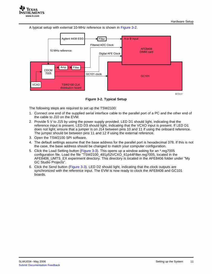
Hardware Setup
A typical setup with external 10-MHz reference is shown in Figure 3-2.
Figure 3-2. Typical Setup
The following steps are required to set up the TSW2100:
1. Connect one end of the supplied serial interface cable to the parallel port of a PC and the other end ofthe cable to J10 on the EVM.
2. Provide 5 V to J15 by using the power supply provided. LED D1 should light, indicating that thereference input is present. LED D3 should light, indicating that the VCXO input is present. If LED D1does not light, ensure that a jumper is on J14 between pins 10 and 11 if using the onboard reference.The jumper should be between pins 11 and 12 if using the external reference.
3. Open the TSW2100 SPI software.4. The default settings assume that the base address for the parallel port is hexadecimal 378. If this is not
the case, the base address should be changed to match your computer configuration.5. Click the Load Setting button (Figure 3-3). This opens up a window asking for an *.reg7005
configuration file. Load the file "TSW2100_491p52VCXO_61p44Filter.reg7005, located in theAFE8406_UMTS_EX experiment directory. This directory is located in the AFE8406 folder under "MyGC Studio Projects".
6. Click the Send button (Figure 3-3). LED D2 should light, indicating that the clock outputs aresynchronized with the reference input. The EVM is now ready to clock the AFE8406 and GC101boards.
SLWU034–May 2006 Setting up the System 11Submit Documentation Feedback

www.ti.com
C004
3.2 Loading and Running a GC Studio Project
3.2.1 ADC Experiments: AFE8406_TESTBUS_EX Directory
3.2.2 UMTS Experiment: AFE8406_UMTS_EX Directory
3.2.3 CDMA2000 Experiment: AFE8406_CDMA2k_EX Directory
Loading and Running a GC Studio Project
Figure 3-3. TSW2100 SPI Software Screen
The simplest way to use GC Studio with the AFE8406 is to open an existing project and to modify itaccording to the application-specific requirements. The following example projects, along with thecorresponding TSW2100 setup files, are included on the Experiments directory:
In these projects, the AFE8406 test bus is used to obtain the internal analog-to-digital converter outputswith a sampling rate of 61.44 Msps and 81.92 Msps. The ADC outputs are decimated by a factor of 32.The MATLAB script AFE8406TestbusPlot.m is provided to measure the signal-to-noise ratio (SNR) andspurious free dynamic range (SFDR) of the signal.
In this project, a UMTS signal with IF frequency of 15.36 MHz, either from analog input or file, isdownconverted. The ADC rate is 61.44 Msps. The NCO mixes the input down to baseband. The mixerbaseband output is upsampled 2× (zero-stuffed) to 122.88 Msps. The zero-stuffed output is decimated 8×by the CIC filter, then decimated 2× by a 32-tap CFIR, with final symbol shaping provided by a 64-tapPFIR. Serial output of the recovered UMTS signal (7.68 Msps) is captured from output port A0 andgraphed spectrally.
In this project, a two-carrier CDMA2000 signal with IF frequency of 8.6432 MHz, either from analog inputor file, is downconverted. The ADC rate is 78.6432 Msps. The NCO mixes the carriers down to baseband.The mixer outputs are decimated 16× by the CIC filter, then decimated 2× by a 32-tap CFIR, with finalsymbol shaping provided by a 64-tap PFIR. Serial outputs of the recovered CDMA2000 signals (2.4576Msps) are captured from output ports A0 and B0 and graphed spectrally.
Setting up the System12 SLWU034–May 2006Submit Documentation Feedback

www.ti.com
3.2.4 DDC AGC Experiment: AFE8406_AGC_EX Directory
3.2.5 Receive-Input AGC Experiment: AFE8406_RAGC_EX Directory
Loading and Running a GC Studio Project
This project demonstrates the adaptation of the DDC’s AGC. The AFE8406 built-in self-test circuit is usedto output a constant which, when multiplied by the NCO, generates a sinusoid signal at the input to theAGC block. Both the PFIR and CFIR have the maximum positive value (131071) programmed into thecorresponding tap0 to allow signal values to pass through the FIRs without being disturbed. In CDMAmode, two signals are present in the interleaved data stream (A and B). To demonstrate the effectivenessof the AGC on both streams, the A and B paths have different AGC gain values. The AGC operationcauses the two signals converge to the same amplitude, one from a lower value (requiring amplification)and one from a higher value (requiring attenuation). Adjusting the agc_gaina_lsb/msb (GAIN_FOR_A) andagc_gainb_lsb/msb (GAIN_FOR_B) values adjusts the amount of change. The rate of change is controlledby the following parameters: agc_dabv, agc_dblw, agc_dsat and agc_dzro.
This project builds on the UMTS experiment and demonstrates the adaptation of the AFE8406 front endand DDC AGCs.
SLWU034–May 2006 Setting up the System 13Submit Documentation Feedback

www.ti.com
C005
C006
C007
Loading and Running a GC Studio Project
To load and run an existing GC Studio project, perform the following steps:• Connect the parallel-port cable to the port connector on the GC101.• Provide power to the GC101 using the power supply provided.• Open the GC Studio program from the Start menu. This opens the main GC Studio window.• Select Open Project… from the File menu. From the CD, select one of the *.gcproj files. This loads the
experiment into GC Studio.
• Click on the Build button. This instructs GC Studio to build the experiment, load it into the GC101 andAFE8406, and capture one frame of data.
• Each of the example projects comes with a set of predefined plots. New plots can be added by clickingon the New Graph button on the top toolbar.
14 Setting up the System SLWU034–May 2006Submit Documentation Feedback
www.ti.com
C008
3.3 Creating a New GC Studio Project
Creating a New GC Studio Project
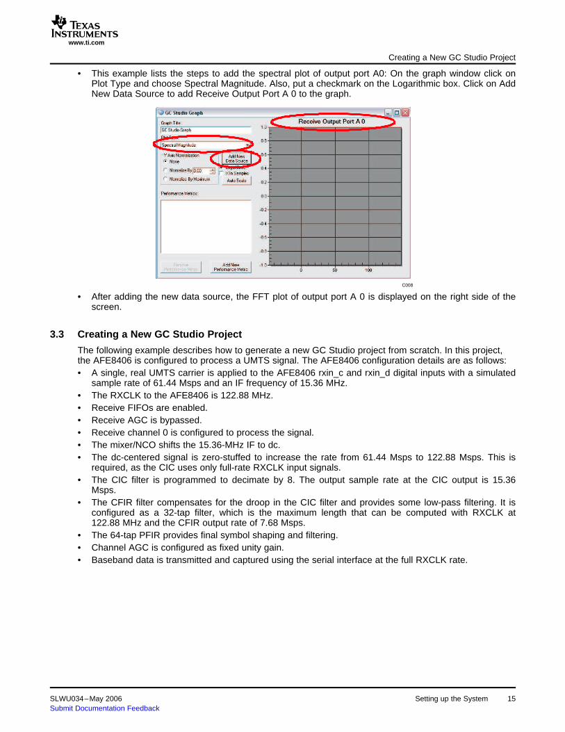
• This example lists the steps to add the spectral plot of output port A0: On the graph window click onPlot Type and choose Spectral Magnitude. Also, put a checkmark on the Logarithmic box. Click on AddNew Data Source to add Receive Output Port A 0 to the graph.
• After adding the new data source, the FFT plot of output port A 0 is displayed on the right side of thescreen.
The following example describes how to generate a new GC Studio project from scratch. In this project,the AFE8406 is configured to process a UMTS signal. The AFE8406 configuration details are as follows:• A single, real UMTS carrier is applied to the AFE8406 rxin_c and rxin_d digital inputs with a simulated
sample rate of 61.44 Msps and an IF frequency of 15.36 MHz.• The RXCLK to the AFE8406 is 122.88 MHz.• Receive FIFOs are enabled.• Receive AGC is bypassed.• Receive channel 0 is configured to process the signal.• The mixer/NCO shifts the 15.36-MHz IF to dc.• The dc-centered signal is zero-stuffed to increase the rate from 61.44 Msps to 122.88 Msps. This is
required, as the CIC uses only full-rate RXCLK input signals.• The CIC filter is programmed to decimate by 8. The output sample rate at the CIC output is 15.36
Msps.• The CFIR filter compensates for the droop in the CIC filter and provides some low-pass filtering. It is
configured as a 32-tap filter, which is the maximum length that can be computed with RXCLK at122.88 MHz and the CFIR output rate of 7.68 Msps.
• The 64-tap PFIR provides final symbol shaping and filtering.• Channel AGC is configured as fixed unity gain.• Baseband data is transmitted and captured using the serial interface at the full RXCLK rate.
SLWU034–May 2006 Setting up the System 15Submit Documentation Feedback

www.ti.com
C003
C009
Creating a New GC Studio Project
To generate the project, follow these steps:
1. Start GC Studio.
2. Select New Project from the File menu and choose a name for the new project. Click create.
16 Setting up the System SLWU034–May 2006Submit Documentation Feedback

www.ti.com
C010
C011
Creating a New GC Studio Project
3. Select AFE8406 for the plug-in and click OK.
4. Click Next> on the Welcome to the GC Studio Project Setup Wizard window.
SLWU034–May 2006 Setting up the System 17Submit Documentation Feedback

www.ti.com
C012
C013
Creating a New GC Studio Project
5. The Evaluation Board Setup appears. It is highly recommended to replicate the setup for one of theexample projects. If a TSW2100 is being used to clock the AFE8406 DIMM and the GC101, under theClock and Sync tab ensure that:
– Stimulus Memory Clock Source is changed to SMA Connector– The correct clock frequency is entered under Input Clock Frequency– The Use Analog PLL box is uncheckedAIf the AFE8406 clock is to be provided by the GC101, modify the AFE8406 DIMM clock path asdescribed in Section 5.4 of this guide. Also ensure the stimulus memory and response memory areconfigured as explained in Section 4.2. After configuring the Evaluation Board Setup, click Next>.
6. Configure the AFE8406 I/O mode. In this example, ensure the ADC clock rate is set to 1/2 and that theRx Sync Offsets and Lengths satisfy the requirements described in Section 4.2. Click Next>.
18 Setting up the System SLWU034–May 2006Submit Documentation Feedback

www.ti.com
C014
C015
Creating a New GC Studio Project
7. Set the simulated clock rate to 122.88 MHz and click Next>.
8. Click Next> on Channel Copying.
SLWU034–May 2006 Setting up the System 19Submit Documentation Feedback

www.ti.com
C016
C017
Creating a New GC Studio Project
9. Enter a description for the project. Click Next>.
10. Click Finish to exit the GC Studio Wizard.
20 Setting up the System SLWU034–May 2006Submit Documentation Feedback

www.ti.com
C018
C019
Creating a New GC Studio Project
11. Click on the large afe8406 box to display the global control registers.
12. Double-click on the afe8406 block to push down one level into the AFE8406. Click on the InputInterface block to display and edit the receive input interface registers. Set rate_sel to HALF; thisconfigures the AFE8406 for input samples at 1/2 the RXCLK rate. Set adc_fifo_bypass to NOTBYPASSED to enable the rxin_a/b/c/d input FIFO circuits.
SLWU034–May 2006 Setting up the System 21Submit Documentation Feedback

www.ti.com
C020
C021
Creating a New GC Studio Project
13. Click on the upper Receive Channel 0 block. Set ddc_ena to True. The topmost receive channel ischanged to green because it has been enabled. Set ddcmux_sel_a to I=ADC2/Q=ADC3; this selectsthe afe8406 digital rxin_c and rxin_d input ports as the I and Q data sources. If the UMTS signal is tobe provided externally, set ddcmux_sel_a to I=ADC0/Q=ADC0.
14. Double-click on the Receive Channel 0 block to push down into this channel. The block diagram nowshows the subblocks in the receive channel, and the registers to configure it. Select the mixer/NCOblock (leftmost block). Set a_frequency to –15.36 MHz. The b_frequency setting is not used when thechannel is in UMTS mode. GC Studio calculates the required values for the phase_add registers andupdates the values after the experiment is run. Set zero_qsample to True. Verify the settings matchthose shown in the following panel.
22 Setting up the System SLWU034–May 2006Submit Documentation Feedback

www.ti.com
C022
C023
Creating a New GC Studio Project
15. Select the Delay Adjust and Zero Stuff block. Because the input sample rate is set to 1/2 the RXCLKrate, this block is automatically configured by GC Studio to interpolation by 2, inserting a zero samplebetween each actual sample before being applied to the CIC filter. This moves the 61.44-Msps inputsignal stream to the 122.88-Msps RXCLK rate. The tadj_offset_coarse and tadj_offset_fine settingsallow the user to adjust the delay between various receive channels if desired.
16. Click on the CIC filter block and set the registers as shown in the following panel. The decimation inthe CIC is set to 8 , resulting in a 15.36-Msps CIC output rate.
17. Select the CFIR block, set cfir_gain to 2.00E-18, and set cra_starttap_cfir to 32 taps. Next, select thecfir_coeff register setting by clicking on it, and then click on the browse button, circled in red on thepreceding panel, to open the Edit Filter window and fill in the CFIR filter tap weights.
SLWU034–May 2006 Setting up the System 23Submit Documentation Feedback

www.ti.com
C024
C025
Creating a New GC Studio Project
18. The CFIR tap weights are entered as shown. Note that the first 20 taps are entered as the first 20entries, and then 12 lines are skipped before entering the second 20. This is due to the AFE8406coefficient RAM being split into two blocks of 32 words. See the AFE8406 data sheet (SLWS168) formore details if necessary. For this example, the CFIR tap weights are:
24 Setting up the System SLWU034–May 2006Submit Documentation Feedback

www.ti.com
C026
C027
Creating a New GC Studio Project
19. Select the PFIR block, set pfir_gain to 2.00E-18, and set crastarttap_pfir to 64. Select the pfir_coeffregister, and again select the browse button.
20. The PFIR tap weights are entered as shown. For the 64-tap PFIR in this example, all coefficients areused. For this example, the PFIR tap weights are:
SLWU034–May 2006 Setting up the System 25Submit Documentation Feedback

www.ti.com
C028
C029
Creating a New GC Studio Project
21. Select the AGC block and set the registers as shown in the following panel. The gain_for_A value isset to unity, and the agc_freeze and agc_clear are both set to True for this example. This puts theAGC in unity fixed-gain mode. GC Studio calculates the required values for the agc_gain registers andupdates the values after the experiment is run.
22. Select the Serial Interface block and set the parameters as indicated.
26 Setting up the System SLWU034–May 2006Submit Documentation Feedback

www.ti.com
C030
Creating a New GC Studio Project
23. After verifying the values for the serial interface, click the arrow circled in red in the preceding panel topop up one level in the AFE8406 hierarchy.Through the preceding steps, receive channel 0 has now been configured as follows:
– UMTS input signal at 61.44 Msps with a 15.36-MHz IF– Mixer/NCO block shifts the signal to dc.– Zero-stuff block interpolates by 2 , moving the 61.44-Msps signal to 122.88 Msps.– CIC block decimates by 8 to 15.36 Msps.– 32-tap CFIR compensates for the CIC droop, filters and decimates the signal to 7.68 Msps.– 64-tap PFIR filters the signal.– Channel AGC is set to a fixed gain of 1.– Serial interface is used to output the baseband signal.AThe AFE8406 daughtercard configuration uses rx_sync_out_6 as the strobe indicating when the serialoutput data starts each transfer. In the following step, the receive channel-0 configuration is copied toreceive channel 6 so the strobe is present in the captured GC101 data.
24. Select AFE8406 Channel Copy from the Parameters menu to bring up the Channel Copy panel. Withchannel 0 selected as the source and channel 6 selected as the destination, click Copy, and then clickOK. The block diagram should now show both channels 0 and 6 active (green).
SLWU034–May 2006 Setting up the System 27Submit Documentation Feedback

www.ti.com
C031
C032
Creating a New GC Studio Project
25. In this example, the input data presented to the AFE8406 comes from data files. Two input file iconscan be seen in the block diagram to the left of the Input Interface block. The upper file icon isconnected to the AFE8406 digital rxin_c input port, and the lower icon is connected to the digital rxin_dinput port. Click on the top icon to show the Receive Input Port 0 menu. Following this, click on thebrowse button to bring up the open file window.
26. Navigate to the AFE8406_UMTS_EX folder and select TM1_600k_1carrier_IF15.36_Fs61.44_I.gcin.Repeat for the lower input file icon, selecting in this case theTM1_600k_1carrier_IF15.36_Fs61.44_Q.gcin file.
28 Setting up the System SLWU034–May 2006Submit Documentation Feedback

www.ti.com
C033
C034
Creating a New GC Studio Project
27. Click on the graph button, circled in red, to open the graph panel.
28. Click the Add New Data Source button and select Receive Output Port A 0.
SLWU034–May 2006 Setting up the System 29Submit Documentation Feedback

www.ti.com
C035
C036
Creating a New GC Studio Project
29. In the graph panel, set the Plot Type to Spectral Magnitude, check the Logarithmic check box, andselect Normalize by Maximum.
30. Connect the GC101 motherboard, AFE8406 daughtercard, and TSW2100 board as described inSection 3.1.
30 Setting up the System SLWU034–May 2006Submit Documentation Feedback
www.ti.com
C047
C048
C037
Creating a New GC Studio Project
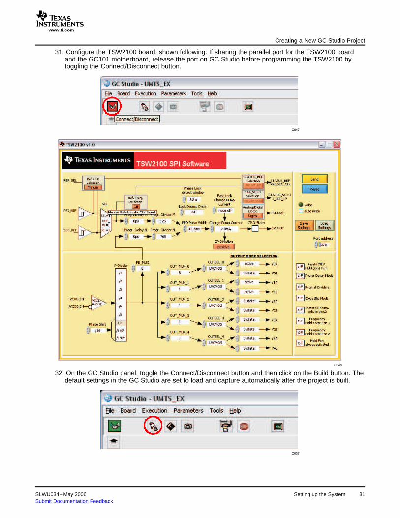
31. Configure the TSW2100 board, shown following. If sharing the parallel port for the TSW2100 boardand the GC101 motherboard, release the port on GC Studio before programming the TSW2100 bytoggling the Connect/Disconnect button.
32. On the GC Studio panel, toggle the Connect/Disconnect button and then click on the Build button. Thedefault settings in the GC Studio are set to load and capture automatically after the project is built.
SLWU034–May 2006 Setting up the System 31Submit Documentation Feedback

www.ti.com
C038
Creating a New GC Studio Project
The graph window is automatically updated with the results.
32 Setting up the System SLWU034–May 2006Submit Documentation Feedback

4.1 Saving the Output to a File
C039
Chapter 4SLWU034–May 2006
Other Options in GC Studio
GC Studio offers much flexibility in evaluating the data processed by the AFE8406.Following is a list of some of these capabilities:
GC Studio allows one to save the data of the AFE8406 to a text file for further analysis by any commercialnumerical analysis software. In this example, the Receive Output Port A0 is saved.
1. Double-click on the AFE8406 block to go into its block diagram. Once there, click on the filecorresponding to Receive Output Port A 0.
SLWU034–May 2006 Other Options in GC Studio 33Submit Documentation Feedback

www.ti.com
C040
4.2 Changing the Data Capture Size
C041
Changing the Data Capture Size
2. Click on the "Save to File" box and select the file to which the data is to be saved.
3. These steps can be repeated for every signal to be captured. Every time the stream is updated, thefiles are also updated with the latest results. The file is saved in decimal format in two columns with thefirst column corresponding to the real portion of the output and the second column to the imaginaryone.
GC Studio allows you to modify the number of samples to be captured. Standard boards are deliveredwith a 1-megaVector (1024-kSample) memory, so ensure that this number is not exceeded.
1. Select EvalBoard Parameter Editor… from the Parameters menu. Once there, go to the ResponseMemory tab and enter the desired number of samples on the Memory Length box.
34 Other Options in GC Studio SLWU034–May 2006Submit Documentation Feedback

www.ti.com
T0124-01
Stimulus memory
Sync length
Sync offset
Captured data is in this region
C042
Changing the Data Capture Size
2. In the current version of GC Studio, the Response Memory capture is triggered by the StimulusMemory. Improper setting of the Stimulus Memory may result in errors in the captured data. Becauseof this, every time the captured data size is modified, it is necessary to corroborate that the StimulusMemory size and the Sync Offset are set up properly.
3. From the foregoing diagram, it is observed that the Sync Offset must be slightly bigger than theResponse Memory size. Also, it is necessary to verify that the Stimulus Memory size is large enough toencompass the Sync Offset and the Sync Length. To adjust the Stimulus Memory size, selectEvalBoard Parameter Editor… from the Parameters menu and go to the Stimulus Memory tab. Enterthe proper number of samples in the Memory Length box.
SLWU034–May 2006 Other Options in GC Studio 35Submit Documentation Feedback

www.ti.com
C043
4.3 Capturing the AFE8406 Test Bus Output
Capturing the AFE8406 Test Bus Output
4. The last step is to modify the Sync Offset and Sync Length so that they match the selected StimulusMemory size. To do this, select AFE8406 I/O Mode Configuration from the Parameters menu. Oncethere, enter the appropriate Sync Offset and Sync Length values in the corresponding boxes. Sync Aand Sync B should have the same values.
The AFE8406 includes a test bus, allowing the user to view internal digital signals. When the test bus isenabled, the rxin_c and rxin_d input ports become outputs and the dvga_c and dvga_d ports aremultiplexed to carry test bus data, giving a 36-bit-wide output port and three additional signals. Becauserxin_c and rxin_d are the test bus outputs, only the analog inputs rxin_a and rxin_b are available in thiscase.
Test Bus Signal Corresponding Signal
testbus(35:0) rxin_d(15:0), dvga_c(3:2), rxin_c(15:0), dvga_c(5:4)
test bus clock dvga_c(1)
test bus sync dvga_c(0)
test bus aflag dvga_d(5)
Other Options in GC Studio36 SLWU034–May 2006Submit Documentation Feedback

www.ti.com
C044
Capturing the AFE8406 Test Bus Output
The GC101 evaluation platform captures a 36-bit signal into the response memory. When selecting thevarious test bus sources, the signals selected in the I/O Mode Selection window must be set correctly.
1. Select AFE8406 I/O Mode Configuration from the Parameters menu. In this menu, set the OutputMode to Test Bus and OutClk to dvga_c(1).
2. The other signals, captured as SyncOut+, Sp5, and Sp6, should be configured as required for thespecific test bus signal [Sp7 is always dvga_c(5)]. The test bus output clock is used to load theresponse memory, and is controlled by the tst_rate_sel.
Test Bus Signal SyncOut+ Sp5 Sp6 OutClk tst_rate_sel
DDC PFIR in UMTS mode dvga_c(2) dvga_c(3) dvga_c(4) dvga_c(1) 2*CIC decimation
DDC PFIR in CDMA mode dvga_c(2) dvga_c(5) dvga_c(4) dvga_c(1) RXCLK rate
DDC CFIR in UMTS mode dvga_c(2) dvga_c(3) dvga_c(4) dvga_c(1) 2*CIC decimation
DDC PFIR in CDMA mode dvga_c(2) dvga_c(5) dvga_c(4) dvga_c(1) RXCLK rate
DDC TADJ-A dvga_c(2) dvga_c(3) dvga_c(4) dvga_c(1) RXCLK rate
DDC TADJ-B CDMA mode only dvga_c(2) dvga_c(3) dvga_c(4) dvga_c(1) RXCLK rate
DDC NCO-SINE in UMTS mode only dvga_c(2) dvga_c(3) dvga_c(4) dvga_c(1) ADC clock rate
DDC NCO-COSINE in UMTS mode only dvga_c(2) dvga_c(3) dvga_c(4) dvga_c(1) ADC clock rate
DDC CIC in UMTS mode dvga_c(2) dvga_c(3) dvga_c(4) dvga_c(1) CIC decimation
DDC CIC in CDMA mode dvga_c(2) dvga_c(5) dvga_c(4) dvga_c(1) RXCLK rate
DDC AGC in UMTS mode dvga_c(2) dvga_c(3) dvga_c(4) dvga_c(1) 2*CIC decimation
DDC AGC in CDMA mode dvga_c(2) dvga_c(5) dvga_c(4) dvga_c(1) RXCLK rate
DDC MIXER-A dvga_c(2) dvga_c(3) dvga_c(4) dvga_c(1) ADC clock rate
DDC MIXER-B CDMA mode only dvga_c(2) dvga_c(3) dvga_c(4) dvga_c(1) ADC clock rate
DDC DDCMUX-A dvga_c(2) dvga_c(3) dvga_c(4) dvga_c(1) ADC clock rate
DDC DDCMUX-B CDMA mode only dvga_c(2) dvga_c(3) dvga_c(4) dvga_c(1) ADC clock rate
RXIN_A and RXINB FIFO dvga_c(2) dvga_c(3) dvga_c(4) dvga_c(1) ADC clock rate
SLWU034–May 2006 Other Options in GC Studio 37Submit Documentation Feedback

www.ti.com
C045
Capturing the AFE8406 Test Bus Output
3. The raw response memory can be captured in a text format by selecting Options… from the Toolsmenu and going to the Debug tab.
The format of the file is hexadecimal, with the 32-bit response memory as the first 8 characters, aspace, and then a single character for the other four special bits (Sp7, Sp6, Sp5, SyncOut+), shown asfollows:…0000F0A0 00000F0A0 028D80000 028D80000 00000F2C6 00000F2C6 026750000 026750000 00000F580 00000F580 0…A
38 Other Options in GC Studio SLWU034–May 2006Submit Documentation Feedback

www.ti.com
C046
Capturing the AFE8406 Test Bus Output
4. To capture the ADC samples, set tst_select to A-B_FIFO_OUTs, and set tst_rate_sel to generate aclock matching the ADC clock rate.
5. Subsequently, the ADC samples can be directed to a graph or to an output file using the stepsdescribed in Section 4.1.
SLWU034–May 2006 Other Options in GC Studio 39Submit Documentation Feedback

www.ti.com
Capturing the AFE8406 Test Bus Output
Other Options in GC Studio40 SLWU034–May 2006Submit Documentation Feedback

B0134-01
CLK+
SP3
adcclk_c
To/From GC101 SWITCH
External power supply
rx_synca
SIGIN[31:16]
SIGIN[15:0]
rxin_c_ovr
SIGOUT[15:0]
rxclk_out
SYNCOUT+
GC101 GC101
From GC101 To GC101
AFE8406 DIMM board
SP1
SYNC+
SP2
CLKOUT+
dvga_c[5]
dvga_c[4]
dvga_c[3]
dvga_c[2]
SP5
SP6
SP7
rx_sync_out
interrupt
SIGOUT[31:16]rxout_7:3_d:a
adcclk_d
rxout_4:0_d:a
[dvga_c[3:0]:dvga_a[5:0]:
dvga_b[5:0]]
rx_sync_out_6
dvga_c[0]
dvga_d[5]
dvga_c[1]
rxin_d_ovr
rx_sync_out_0
rxin_c[15:0]
rxin_d[15:0]
rx_syncb
AFE8406
Tristate buffercontrol register
TTJTAGMPU Interface[a(6), d(16), rd_n,wr_n, ce_n,reset_n],Power/Gnd
5.1 AFE8406 Daughtercard Pin Description
Chapter 5SLWU034–May 2006
AFE8406 Daughtercard Description
AFE8406 DIMM–GC101 Interface Block Diagram
The AFE8406 daughtercard has a PC-133 form-factor that uses the 168-pin daughtercard memoryconnector. The 168-pin interface signals are divided into groups as listed in Table 5-1 thhrough Table 5-6.
Table 5-1. Memory Input Bus—36 Data Inputs Used to Stimulate the AFE8406 Inputs
Signal Alias Description
SIGIN(35) SP3 Clock gating signal for adcclk_a and adcclk_b
SIGIN(34) SP2 rxin_c_ovr and rxin_d_ovr input signals
SIGIN(33) SP1 rx_syncb input signal
SIGIN(32) SYNC+ rx_synca input signal
SLWU034–May 2006 AFE8406 Daughtercard Description 41Submit Documentation Feedback

www.ti.com
AFE8406 Daughtercard Pin Description
Table 5-1. Memory Input Bus—36 Data Inputs Used to Stimulate the AFE8406 Inputs (continued)
Signal Alias Description
SIGIN(31:16) rxin_c(15:0) input data
SIGIN(15:0) rxin_d(15:0) input data
Table 5-2. Memory Output Bus—36 Data Outputs From Selected AFE8406 Outputs Captured by theGC101
Signal Alias Description
SIGOUT(35) SP7 dvga_c(5)
SIGOUT(34) SP6 dvga_c(4) or rx_sync_out_0
SIGOUT(33) SP5 dvga_c(3), dvga_d(5) or interrupt
SIGOUT(32) SYNCOUT+ rx_sync_out, rx_sync_out_6, dvga_c(0) or dvga_c(2)
SIGOUT(31:16) rxout_7:4_d:a baseband DDC data or rxin_d(15:0) testbus output
SIGOUT(15:0) rxout_3:0_d:a baseband DDC data or rxin_c(15:0) testbus output
Table 5-3. Clock
Signal Description
CLK+ RXCLK clock for AFE8406; can be used as a full-rate or gated clock source when combinedwith the gating signal SP3 for the adcclk_a and adcclk_b inputs.
CLKOUT Clock signal from the daughtercard to the GC101; RXCLK, rxclk_out from the GC5018 ordvga_c(1)
Table 5-4. Microprocessor Control Bus—Bus to Program the Internal Registers
Signal Description
d(15:0) Control data I//O bus, active-high bidirectional I/O pins. This is the 16-bit control data I/Obus. Control registers are written to or read from through these pins. The chip drives thesepins when CE is low, RD is low, and WR is high.
A(10:0) Control address bus, active-high inputs. These pins are used to address the control registerswithin the chip. Each of the control register within the chip is assigned a unique address. Acontrol retister can be written to or read from by having the page register set to theappropriate page and then setting A(10:0) to the register address.
CE, RD, WR, and RST ce_n, rd_n, wr_n and rst_n on the AFE8406
Table 5-5. JTAG
Signal Description
JTAG 5-pin JTAG test port for AFE8406
TRST, TCK, TMS, TDI, TDO trst_n, tck, tms, tdi, and tdo on the AFE8406
Table 5-6. Power and Ground
Signal Description
VDUT1 3.3-V power from GC101 EVM to the daughtercard
GND Return path for the daughtercard
See the GC101 EVM User's Guide (SLWU018) for the 168-pin connector table. Detailed schematics forthe AFE8406 daughtercard can be found in Chapter 6.
AFE8406 Daughtercard Description42 SLWU034–May 2006Submit Documentation Feedback

www.ti.com
5.2 AFE8406 Daughtercard Jumpers
5.3 AFE8406 Daughtercard Power Supplies
5.4 AFE8406 Daughtercard Clock Configurations
AFE8406 Daughtercard Jumpers
The following table describes the various jumpers on the AFE8406 daughtercard card:
Jumper Description
J7 pin_configure signal to ADC. Selects normal operating mode when jumper is in 1:2 (center:on) position (default).Selects serial interface mode when jumper is in 2:3 (off:center) position.
J8 Enables ADC A outputs when jumper is in 1:2 (center:on) position (default). Disables ADC A outputs when jumper isin 2:3 (off:center) position.
J9 Enables ADC B outputs when jumper is in 1:2 (center:on) position (default). Disables ADC B outputs when jumper isin 2:3 (off:center) position.
J11 Clock doubler power down for the CDC5801. Position 1:2 (center:on) 3.3 V, enabled (default). Position 2:3 (off:center)0 V, powered down.
J12 1× or 2× clock select for the CDC5801. Position 1:2 (center:on) 3.3 V, 2× output clock. Position 2:3 (off:center) 0 V, 1×output clock.
W14 3.3-V fuse power for ADC. Position 1:2 (center:on) 3.3 V, normal operation (default). Position 2:3 (off:center) 0 V –DO NOT USE THIS POSITION.
W15 3.3-V fuse power for the GC5018. Position 1:2 (center:on) 3.3 V, normal operation (default). Position 2:3 (off:center) 0V – DO NOT USE THIS POSITION.
J17 Pins 1:2—ADC DLL disabled when jumper removed (default). Pins 3:4—ADC internal reference when installed(default). Pins 5:6—ADC operational when installed (default).
W13 External DVDD power supply. Position 1:2 (center:on) internal 1.5 V to DVDD (default). Position 2:3 (off:center)external 1.5 V through J24.
W25 External AVDD power supply. Position 1:2 (center:on) internal 3.3 V to AVDD (default). Position 2:3 (off:center)external 3.3 V through J29.
W26 External VDDS power supply. Position 1:2 (center:on) internal 3.3 V to VDDS (default). Position 2:3 (off:center)external 3.3 V through J30.
W27 External DRVDD power supply. Position 1:2 (center:on) internal 3.3 V to DRVDD(default). Position 2:3 (off:center)external 3.3 V through J28.
J23 1.5-V regulator software control using c10 register bit – DO NOT INSTALL.
The AFE8406 I/O and core power supplies are 3.3 V and 1.5 V, respectively. The default configuration ofthe AFE8406 daughtercard enables the GC101 motherboard to supply 3.3 V to the daughtercard, whichincludes a 1.5-V regulator. Alternatively, by modifying jumpers W13, W25, W26 and W27, external powersupplies can be used to provide these voltages to the daughtercard.
The AFE8406 daughtercard card allows for the following clock configurations:
1. Default configuration (to be used with TSW2100): AFE8406 daughtercard RX clock SMA input
– Input RX clock rate at J5 (CLKM)– Install 0-Ω resistors in
• R40• R72• R58
– Remove resistors in
• R36• R43• R52• R73
– For CDCF5801 at 1 , install
• J12 jumper between pins 2 and 3– For CDCF5801 at 2 , install
• J12 jumper between pins 1 and 2
SLWU034–May 2006 AFE8406 Daughtercard Description 43Submit Documentation Feedback

www.ti.com
AFE8406 Daughtercard Clock Configurations
– Clock path:J5 → R40 → R72 → C137 → U22 (pin2) → U22 (pin20) → R58 → AFE8406 (ball r22)
2. Configuration for AFE8406 daughtercard RX clock from GC101 (through CDCF5801)
– Install 0-Ω resistors in
• R46• R70• R73• R58
– Remove resistors in
• R36• R43• R52• R72
– For CDCF5801 at 1 , install
• J12 jumper between pins 2 and 3– For CDCF5801 at 2 , install
• J12 jumper between pins 1 and 2– Clock path:
J16A (pin 34) → R46 → C148 → U2 (pin1) → U2 (pin2) → R70 →R73 → C137 → U22 (pin2) →U22 (pin20) → R58 → AFE8406 (ball r22)
3. Configuration for AFE8406 daughtercard RX clock from GC101 (bypass CDCF5801)
– Install 0-Ω resistors in
• R46• R36• R73
– Remove resistors in
• R43• R52• R73• R72• R58
– Clock path:J16A (pin 34) → R46 → C148 → U2 (pin1) → U2 (pin2) → R36 → AFE8406 (ball r22)
4. Configuration for AFE8406 daughtercard RX clock from ADC clock (GC101 separate)
– Install 0-Ω resistors in
• R52• R58
– Remove resistors in
• R36• R43• R52• R72• R73
– For CDCF5801 at 1 , install
• J12 jumper between pins 2 and 3– For CDCF5801 at 2 , install
• J12 jumper between pins 1 and 2– Clock path:
J6 (CLKP) → R52 → C137 → U22 (pin2) → U22 (pin20) → R58 → AFE8406 (ball r22)
44 AFE8406 Daughtercard Description SLWU034–May 2006Submit Documentation Feedback

6.1 PCB Layout
K001
Chapter 6SLWU034–May 2006
Physical Description
This chapter describes the physical characteristics and PCB layout of the AFE8406daughtercard and lists the components used on the module.
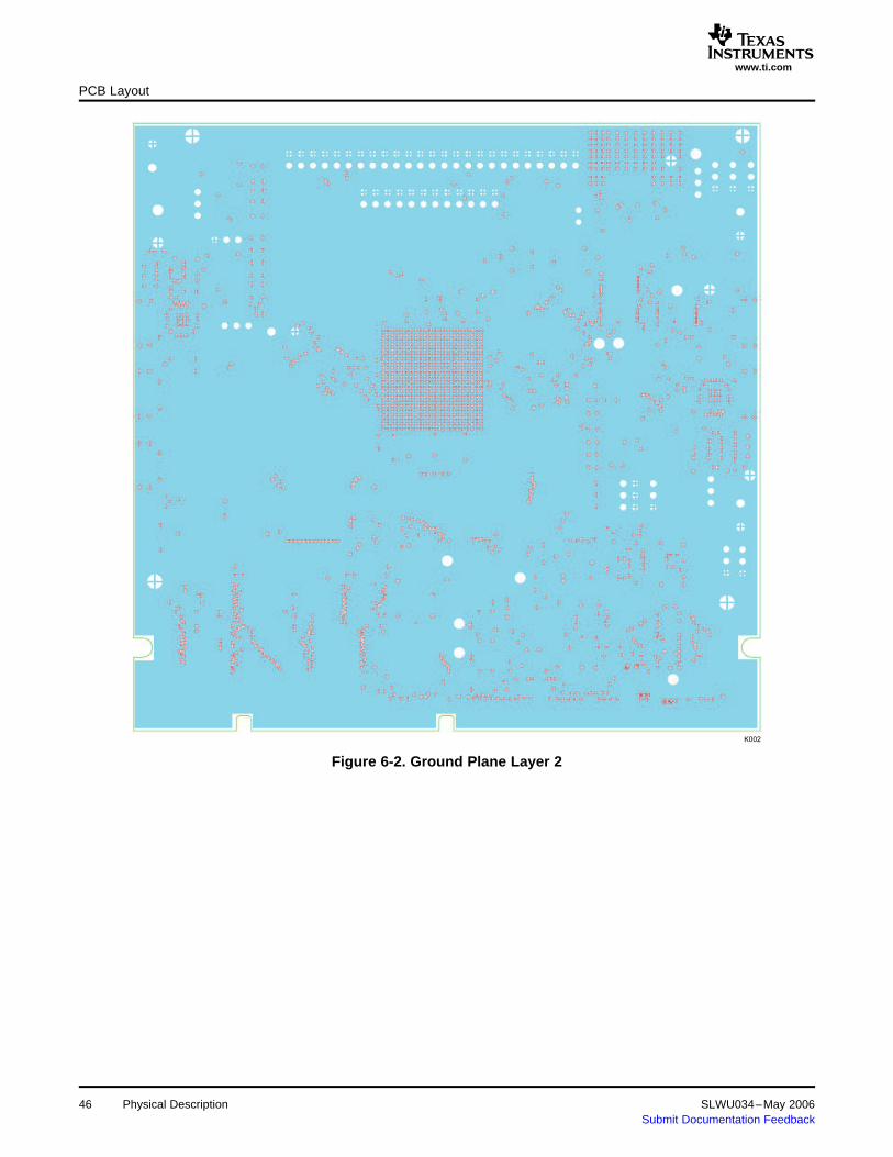
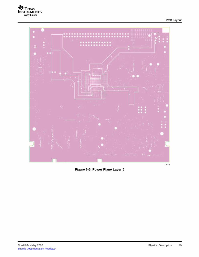
The board is constructed on an 8-layer, 5.11-inch x 5.25-inch, 0.056-inch thick PCB using FR-4 material.Figure 6-1 through Figure 6-8 show the PCB layout for the daughtercard.
Figure 6-1. Top Layer 1
SLWU034–May 2006 Physical Description 45Submit Documentation Feedback
www.ti.com
K002
PCB Layout
Figure 6-2. Ground Plane Layer 2
46 Physical Description SLWU034–May 2006Submit Documentation Feedback

www.ti.com
K003
PCB Layout
Figure 6-3. Signal Layer 3
SLWU034–May 2006 Physical Description 47Submit Documentation Feedback

www.ti.com
K004
PCB Layout
Figure 6-4. Signal Layer 4
48 Physical Description SLWU034–May 2006Submit Documentation Feedback
www.ti.com
K005
PCB Layout
Figure 6-5. Power Plane Layer 5
SLWU034–May 2006 Physical Description 49Submit Documentation Feedback

www.ti.com
K006
PCB Layout
Figure 6-6. Signal Layer 6
50 Physical Description SLWU034–May 2006Submit Documentation Feedback

www.ti.com
K007
PCB Layout
Figure 6-7. Ground Plane Layer 7
SLWU034–May 2006 Physical Description 51Submit Documentation Feedback

www.ti.com
K008
6.2 Parts List
Parts List
Figure 6-8. Bottom Layer 8
Table 6-1 lists the parts used in constructing the AFE8406 daughtercard.
Table 6-1. AFE8406 Daughtercard Bill of Materials (BOM)
Part Reference Value Mfr_Name Mfr_Part_Number Quantity Note
C1, C2, C3, C9, C10, C138, C139, 0.01 µF Panasonic ECJ-0EF1E103Z 15C149, C150, C151, C152, C153,C154, C157, C158
C4, C5 10 pF Panasonic ECJ-0EC1H100D 0 Do not install
C6 10 pF Panasonic ECJ-0EC1H100D 1
C7, C8 27 pF Panasonic ECJ-0EC1H270J 0 Do not install
52 Physical Description SLWU034–May 2006Submit Documentation Feedback

www.ti.com
Parts List
Table 6-1. AFE8406 Daughtercard Bill of Materials (BOM) (continued)
Part Reference Value Mfr_Name Mfr_Part_Number Quantity Note
C13, C14, C15, C16, C17, C18, 0.1 µF Panasonic ECJ-0EB1A104K 84C20, C21, C23, C24, C25, C26,C27, C28, C29, C31, C32, C33,C36, C37, C38, C40, C42, C45,C47, C48, C49, C51, C54, C57,C58, C59, C61, C63, C64, C65,C66, C67, C68, C69, C70, C71,C73, C74, C75, C76, C77, C78,C79, C80, C81, C82, C83, C84,C85, C86, C111, C114, C116, C117,C118, C122, C124, C126, C127,C128, C129, C130, C131, C132,C133, C134, C135, C136, C137,C140, C141, C142, C144, C146,C147, C148, C156, 159
C19 0.1 µF Panasonic ECJ-0EB1A104K 0 Do not install
C39, C43, C62, C72, C112, C115, 10 µF Panasonic ECS-T1AX106R 10C119, C123, C145, C155
C110, C125 1 µF Panasonic ECJ-1VB1A105K 2
C113, C120, C121, C143 47 µF Panasonic ECS-T1AD476R 4
C160 12 pF Panasonic ECJ-0EC1H120D 1
FB2, FB3, FB4, FB5, FB6 Ferrite bead Panasonic EXC-ML32A680U 5
FB7 Ferrite bead ? ? 1
FB8 Ferrite bead 0 Do not install
J1, J2, J3, J4, J5, J6, J13 SMA_END_RND Johnson 142-0711-821 7Components
J10 Header Samtec TSW-112-07-L-D 1
J7,J8, J9, J11, J12, W13, W14, Header_1x3_100_430L Samtec TSW-103-07-L-S 11W15, W25, W26, W27
J17 Header_2x3_100_430L Samtec TSW-103-07-L-D 1
J18 TSW-125-07-L-D Samtec TSW-125-07-L-D 1
J19, J20, J21, J22 Standoff Allied 1902CK 4
J23 Header_1x2_100_430L Samtec TSW-102-07-L-S 1
J24, J28, J29, J30 Header_1x2_100_430L On-Shore ED120/2DS 4Technology
PP1 PROBE_POINT 0 Do not install
R2, R17, R23, R25, R40, R46, R57, 0 Ω Panasonic ERJ-3GEY0R00V 13R61, R62, R63, R67, R71, R72
R3, R4, R10, R18, R19, R24 0 Ω Panasonic ERJ-8GEY0R00V 0 Do not install
R5, R6, R7, R8, R11, R12, R13, 24.9 Ω Panasonic ERJ-3EKF24R9V 8R14
R9, R15 174 Ω Panasonic ERJ-2RKF1740X 0 Do not install
R16, R33, R43, R52, R69, R70, 0 Ω Panasonic ERJ-3GEY0R00V 0 Do not installR73, R81, R116
R20, R21, R28, R29 1 Ω Yaego 9C0603A1 JLHFT 4America
R22, R74, R77, R78 49.9 Ω Panasonic ERJ-3EKF49R9V 0 Do not install
R26, R31, R34, R59, R60 10 kΩ Panasonic ERJ-3EKF1002V 5
R47, R48, R49 49.9 kΩ Panasonic ERJ-3EKF4992V 3
R27 49.9 Ω Panasonic ERJ-2RKF49R9X 1
R30 56.2 kΩ Panasonic ERJ-3EKF5622V 1
R32 10 kΩ Panasonic ERJ-3EKF1002V 0 Do not install
R35, R37, R58 10 Ω Panasonic ERJ-3EKF10R0V 3
SLWU034–May 2006 Physical Description 53Submit Documentation Feedback

www.ti.com
Parts List
Table 6-1. AFE8406 Daughtercard Bill of Materials (BOM) (continued)
Part Reference Value Mfr_Name Mfr_Part_Number Quantity Note
R36 10 Ω Panasonic ERJ-3EKF10R0V 0 Do not install
R38, R39 130 Ω Panasonic ERJ-3EKF1300V 0 Do not install
R41 6.81 kΩ Panasonic ERJ-3EKF6811V 1
R42 30.1 kΩ Panasonic ERJ-3EKF3012V 1
R44, R45 100 Ω Panasonic ERJ-3EKF1000V 2
R50, R51, R53, R54, R55, R56, 4.75 kΩ Panasonic ERJ-3EKF4751V 16R64, R107, R108, R109, R110,R111, R112, R113, R114, R115
R65, R66 130 Ω Panasonic ERJ-3EKF1300V 2
R68 4.75 kΩ Panasonic ERJ-3EKF4751V 0 Do not install
R75, R76 0 Ω Panasonic ERJ-3GEY0R00V 0 Do not install
R79, R105 150 Ω Panasonic ERJ-2RKF1500X 0 Do not install
R80, R82, R83, R84, R85, R86, 130 Ω Panasonic ERJ-2RKF1740X 24R87, R88, R89, R90, R91, R92,R93, R94, R95, R96, R97, R98,R99, R100, R101, R102, R103,R104
SW1 EVQPJX Panasonic EVQPJX04M 1
T1, T2, T3 ADT1-1WT Minicircuits ADT1-1WT 3
TP1, TP2, TP3, TP7, TP8, TP9, Red Keystone 5000 10TP10, TP11, TP12, TP15
TP4, TP5, TP6, TP13 Blk Keystone 5001 4
U1 AFE8406 TI AFE8406IZDQ 1
U2 CDCVF2505 TI CDCVF2505D 1
U3 74LVC1G02 TI 74LVC1G02DBV 1
U4, U9, U21, U23, U24 SN74LVC1G04 TI SN74LVC1G04DBV 5
U5, U6, U19, U20 SN74CBTLV1G125 TI SN74CBTLV1G125DBV 4
U7 SN74ALVTH16374 TI SN74ALVTH16374GR 1
U8 TPS75701 TI TPS75701KTT 1
U10 SN74LVC08A TI SN74LVC08APWR 1
U11, U12, U13, U14, U15 SN74CBTLV16210 TI SN74CBTLV16210GR 5
U16, U17, U18 SN74CBTLV3253 TI SN74CBTLV3253PWR 3
U22 CDCF5801 TI CDCF5801DBQ 1
U25, U26 AA113-310 Skyworks AA113-310 2
U27, U28 SN74LVCC3245A TI SN74LVCC3245APWR 2
U29 CDCVF2505 TI CDCVF2505PW 1
Physical Description54 SLWU034–May 2006Submit Documentation Feedback

Chapter 7SLWU034–May 2006
AFE8406 Daughtercard Schematics
This chapter contains the AFE8406 schematic diagrams.
SLWU034–May 2006 AFE8406 Daughtercard Schematics 55Submit Documentation Feedback

5
5
4
4
3
3
2
2
1
1
D D
C C
B B
A A
INPA
GCD0GCD1GCD2GCD3GCD4GCD5GCD6GCD7GCD8GCD9GCD10GCD11GCD12GCD13GCD14
INPBINMB
50ohm_6 Diffpair_6
GCA0GCA1GCA2GCA3GCA4GCA5
GCD15
DVGA0DVGA1DVGA2DVGA3DVGA4DVGA5
DVGA6DVGA7DVGA8DVGA9DVGA10DVGA11
DVGA12DVGA13DVGA14DVGA15
DVGAD0DVGAD1DVGAD2DVGAD3DVGAD4DVGAD5
50ohm_5Diffpair_5Diffpair_5
INMA
+3.3V
+3.3V
+3.3V+3.3V
+3.3V
+3.3V
CMA
CMB
CLKPA
CLKMA
CLKPACLKMA
SCLKSEN
SDI
ADCCLK
RXCLK
GCD[0..15]
GCA[0..5]
DVGA[0..15]
DVGAD[0..5]
DVGA_C5DVGA_C4
CLKIN
SP2
INTERRUPT
TDO
RD_NWR_NCE_N
GCRSTN
TDITMS
TCLKC11
SDISENSCLK
CLKIN
INPAINMAINPBINMB
Title
Size Document Number Rev
Date: Sheet ofAFE8406 EVM SCH D2
AFE8406 EVM
B1 7Tuesday, May 02, 2006
Title
Size Document Number Rev
Date: Sheet ofAFE8406 EVM SCH D2
AFE8406 EVM
B1 7Tuesday, May 02, 2006
Title
Size Document Number Rev
Date: Sheet ofAFE8406 EVM SCH D2
AFE8406 EVM
B1 7Tuesday, May 02, 2006
(2-3)
(1-2)(3-4)(5-6)
(1-2)
(1-2)
(Sh 6)
(Sh 6)
(Sh 7) (Sh 7)
(Sh 7)
(Sh 5)
(Sh 5)
(Sh 7)
(Sh 5)
(Sh 7)(Sh 7)(Sh 7)
(Sh 6)
(Sh 2)
(Sh 5)
(Sh 3)
(Sh 3)
(Sh 3)
(Sh 3)
(Sh 3)
(Sh 3)
(Sh 3)
ASHLEY TRAN
12500 TI Boulevard. Dallas, Texas 75243
Engineer:
Drawn By:
J. SETON
FILE:
R21 20
5%1/10W
R21 20
5%1/10W
R330
1%1/10W
DNIR330
1%1/10W
DNI
C15.1UFC15.1UF
12
SW1
EVQPJX
SW1
EVQPJX
21
R24 0Do Not Install
5%1/4W
R24 0Do Not Install
5%1/4W
R105150
1%1/16WDNIR105150
1%1/16WDNI
C20.1UFC20.1UF
12
R3110K
1%1/10W
R3110K
1%1/10W
R4949.9K
1%1/10W
R4949.9K
1%1/10W
R400
1%1/10W
R400
1%1/10W
C13
.1UF
DNIC13
.1UF
DNI
1 2
R644.75K
1%1/10W
R644.75K
1%1/10W
R1160
1%1/10W
Do Not InstallR1160
1%1/10W
Do Not Install
C14.1UFC14.1UF
12R22
49.9
1%1/10W
Do Not InstallR2249.9
1%1/10W
Do Not Install
C10
.01UF
C10
.01UF
1 2
MS A
DE N
J5CLKM
MS A
DE N
J5CLKM
1
5234
R250
1%1/10W
R250
1%1/10WR43 0
1%1/10WDo Not Install
R43 0
1%1/10WDo Not Install
C16
.1UF
DNIC16
.1UF
DNI
1 2
R230
1%1/10W
R230
1%1/10W
C18.1UFC18.1UF
12
J7J7123
R3056.2K
1%1/10W
R3056.2K
1%1/10W
R4749.9K
1%1/10W
R4749.9K
1%1/10W
R79150
1%1/10W
DNIR79150
1%1/10W
DNI
J9J9123
R19 0Do Not Install
5%1/4W
R19 0Do Not Install
5%1/4W
R2749.9
1%1/16W
R2749.9
1%1/16W
T3ADT1-1WT
T3ADT1-1WT
3
2
1 6
5
4
R3210K
1%1/10W
Do Not InstallR3210K
1%1/10W
Do Not Install
C9
.01UF
C9
.01UF
1 2
R28 20
5%1/10W
R28 20
5%1/10W
R62 0
1%1/10W
R62 0
1%1/10W
R7849.9
1%1/10W
Do Not InstallR7849.9
1%1/10W
Do Not Install
J8J8123
R20 20
5%1/10W
R20 20
5%1/10W
J17J1713
24
56
MS A
DE N
J6CLKP
MS A
DE N
J6CLKP
1
5234
R29 20
5%1/10W
R29 20
5%1/10WC17.1UFC17.1UF
12
R520
1%1/10W
Do Not InstallR520
1%1/10W
Do Not Install
U1D
AFE8406
U1D
AFE8406
INPAF3INMAF4INPBV4INMBV3
CLKPAH1CLKMAJ1CLKPBR1CLKMBT1
REFPAL3REFMAK3REFPBP3REFMBN3
IREFM3
PIN_CONFIGT5
dll_enable/SDIN10pwdn/SCLKM9ext_ref/SENM10
OEAL9OEBN9
FUSE_SELH5RXCLKR22
ADCCLK_CAA11ADCCLK_DAB11
RXIN_A_OVRG6RXIN_B_OVRN8RXIN_C_OVRAB6RXIN_D_OVRV12
D0Y22D1Y21D2AB20D3AA20D4Y20D5W20D6V20D7AB19D8AA19D9Y19D10W19D11V19D12AB18D13AA18D14Y18D15W18
A0T20A1U22A2U21A3W22A4V21A5W21
RD_NT22WR_NR20CE_NT21RESET_NR21
TDIK22TMSK21TRST_NJ22TCLKL20
TDO L21
INTERRUPT M21
CMA H3
CMB T3
DVGA_A_0 C8DVGA_A_1 A7DVGA_A_2 B7DVGA_A_3 C7DVGA_A_4 D8DVGA_A_5 D7
DVGA_B_0 B9DVGA_B_1 C9DVGA_B_2 D10DVGA_B_3 D9DVGA_B_4 A8DVGA_B_5 B8
DVGA_C_0 AA16DVGA_C_1 Y16DVGA_C_2 W16DVGA_C_3 V16DVGA_C_4 AB15DVGA_C_5 AA15
DVGA_D_0 V18DVGA_D_1 AB17DVGA_D_2 AA17DVGA_D_3 W17DVGA_D_4 V17DVGA_D_5 AB16
R4849.9K
1%1/10W
R4849.9K
1%1/10W
C19.1UFDNI
C19.1UFDNI
12

5
5
4
4
3
3
2
2
1
1
D D
C C
B B
A A
RXIN_D0RXIN_D1RXIN_D2RXIN_D3RXIN_D4RXIN_D5RXIN_D6RXIN_D7RXIN_D8RXIN_D9RXIN_D10RXIN_D11RXIN_D12RXIN_D13RXIN_D14RXIN_D15
RXIN_C0RXIN_C1RXIN_C2RXIN_C3RXIN_C4RXIN_C5RXIN_C6RXIN_C7RXIN_C8RXIN_C9RXIN_C10RXIN_C11RXIN_C12RXIN_C13RXIN_C14RXIN_C15
RXOUT16RXOUT17RXOUT18RXOUT19
RXOUT20RXOUT21RXOUT22RXOUT23
RXOUT24RXOUT25RXOUT26RXOUT27
RXOUT28RXOUT29RXOUT30RXOUT31
RXOUT12RXOUT13RXOUT14RXOUT15
RXOUT11RXOUT10RXOUT9RXOUT8
RXOUT7RXOUT6RXOUT5RXOUT4
RXOUT3RXOUT2RXOUT1RXOUT0
+3.3V
+3.3V
+3.3V
+3.3V
+3.3V+3.3V
+3.3V
+3.3V
CLK+
RXCLK
CLKOUT
C7
ADCCLK
RX_SYNCBRX_SYNCA
RXIN_C[0..15]
RXIN_D[0..15]
RXOUT[0..15]RXOUT[16..31]
RX_SYNC_OUTRXCLK_OUT
RX_SYNC_OUT_6
SP3
RX_SYNC_OUT_0
CLKIN
BUFFIN
Title
Size Document Number Rev
Date: Sheet ofAFE8406 EVM SCH D2
AFE8406 EVM
B2 7Tuesday, May 02, 2006
Title
Size Document Number Rev
Date: Sheet ofAFE8406 EVM SCH D2
AFE8406 EVM
B2 7Tuesday, May 02, 2006
Title
Size Document Number Rev
Date: Sheet ofAFE8406 EVM SCH D2
AFE8406 EVM
B2 7Tuesday, May 02, 2006
(Sh 3)
(Sh 6)
(Sh 6)
(Sh 6)
(Sh 5)
(Sh 3)
(Sh 3)
(Sh 3)
(Sh 3)
(Sh 3)
(Sh 1)
(Sh 5)
(Sh 5)
(Sh 6)
ASHLEY TRAN
12500 TI Boulevard. Dallas, Texas 75243
Engineer:
Drawn By:
J. SETON
FILE:
U2CDCVF2505D
U2CDCVF2505D
CLK1 3
CLK2 2
CLK3 5
CLK4 7
CLKOUT 8
REF1
VDD6
GND4
R69 0
1%1/10WDo Not Install
R69 0
1%1/10WDo Not Install
R36 10
1%1/10W
Do Not InstallR36 10
1%1/10W
Do Not Install
R2610K
1%1/10W
R2610K
1%1/10W
C610PFC610PF
12
O
U3
74LVC1G02
O
U3
74LVC1G02
1
23
45
R38130
1%1/10W
Do Not Install
R38130
1%1/10W
Do Not Install
C23
.1UF
C23
.1UF1 2
U674CBTLV1G125U674CBTLV1G125
A2
OE1
B 4V
CC
5G
ND
3
R67 0
1%1/10W
R67 0
1%1/10W
R37 10
1%1/10W
R37 10
1%1/10W
R66130
1%1/10W
R66130
1%1/10W
C24
.1UF
C24
.1UF1 2
PP1 Do Not InstallPP1 Do Not Install1
U4
74LVC1G04
U4
74LVC1G04
42
53
J10J10
1 2468101214161820
3579
111315171921 2223 24
U1E
AFE8406
U1E
AFE8406
RXIN_C_0W11 RXIN_C_1AB10 RXIN_C_2AA10 RXIN_C_3Y10 RXIN_C_4W10 RXIN_C_5AB9 RXIN_C_6AA9 RXIN_C_7Y9 RXIN_C_8W9 RXIN_C_9AB8 RXIN_C_10AA8 RXIN_C_11V10 RXIN_C_12Y8 RXIN_C_13AB7 RXIN_C_14AA7 RXIN_C_15Y7
RXIN_D_15W12RXIN_D_14Y12RXIN_D_13AA12RXIN_D_12AB12RXIN_D_11V13RXIN_D_10W13RXIN_D_9Y13RXIN_D_8AA13RXIN_D_7AB13RXIN_D_6V14RXIN_D_5W14RXIN_D_4AA14RXIN_D_3AB14RXIN_D_2V15RXIN_D_1W15RXIN_D_0Y15
RX_SYNCAP21RX_SYNCBP22RX_SYNCCN20RX_SYNCDN21
TESTMODE0G21TESTMODE1G22SCANENH21
FA002_SCANJ20FA002_CLKH22
ZEROH20
FUSE_OUTF20FUSE_ENAD21FUSE_BIASF21FA002_OUTJ21
RX_SYNC_OUT_7 A20
RX_SYNC_OUT_0 A10RX_SYNC_OUT_1 C12RX_SYNC_OUT_2 B13RX_SYNC_OUT_3 D15RX_SYNC_OUT_4 C16RX_SYNC_OUT_5 C17RX_SYNC_OUT_6 C19
RXOUT_0_A B11RXOUT_0_B C11RXOUT_0_C B10RXOUT_0_D A9
RXOUT_1_A A12RXOUT_1_B B12RXOUT_1_C D12RXOUT_1_D A11
RXOUT_2_A D14RXOUT_2_B A13RXOUT_2_C C13RXOUT_2_D D13
RXOUT_3_A B15RXOUT_3_B C15RXOUT_3_C A14RXOUT_3_D B14
RXOUT_4_A A16RXOUT_4_B B16RXOUT_4_C D16RXOUT_4_D A15
RXOUT_5_A D18RXOUT_5_B B17RXOUT_5_C D17RXOUT_5_D A17
RXOUT_6_A A19RXOUT_6_B B19RXOUT_6_C A18RXOUT_6_D B18
RXOUT_7_A D20RXOUT_7_B C21RXOUT_7_C B20RXOUT_7_D C20
DVDDMON L22DVSSMON M22
RX_SYNC_OUT E22RXCLK_OUT E21
C21.1UFC21.1UF
12
C25
.1UF
C25
.1UF1 2
R3410K
1%1/10W
R3410K
1%1/10W
R70 0
1%1/10W
Do Not InstallR70 0
1%1/10W
Do Not InstallC148
.1UF
C148
.1UF1 2
U574CBTLV1G125U574CBTLV1G125
A2
OE1
B 4
VC
C5
GN
D3
R65130
1%1/10W
R65130
1%1/10W
C142
.1UF
C142
.1UF1 2
R39130
1%1/10W
Do Not Install
R39130
1%1/10W
Do Not Install
R1154.75K
1%1/10W
R1154.75K
1%1/10W
R35 10
1%1/10W
R35 10
1%1/10W

5
5
4
4
3
3
2
2
1
1
D D
C C
B B
A A
GCD0GCD1
GCD3GCD2
GCD4GCD5
GCD6GCD7GCD8GCD9
GCD10GCD11
GCD12GCD13
GCD15GCD14
GCD15GCD14GCD13GCD12GCD11
GCD9GCD8GCD7GCD6GCD5GCD4
GCD2GCD1GCD0
GCA0GCA1GCA2GCA3GCA4GCA5
GCD3
GCD10
DATA_D0DATA_D1DATA_D2DATA_D3DATA_D4DATA_D5DATA_D6DATA_D7DATA_D8DATA_D9DATA_D10DATA_D11DATA_D12DATA_D13DATA_D14DATA_D15
DATA_C0DATA_C1DATA_C2DATA_C3DATA_C4DATA_C5DATA_C6DATA_C7DATA_C8DATA_C9DATA_C10DATA_C11DATA_C12DATA_C13DATA_C14DATA_C15 RXOUT31
RXOUT30RXOUT29RXOUT28RXOUT27RXOUT26RXOUT25RXOUT24RXOUT23RXOUT22RXOUT21RXOUT20RXOUT19RXOUT18RXOUT17RXOUT16
RXOUT15RXOUT14RXOUT13RXOUT12RXOUT11RXOUT10RXOUT9RXOUT8RXOUT7RXOUT6RXOUT5RXOUT4RXOUT3RXOUT2RXOUT1RXOUT0
DATA_C0DATA_C1DATA_C2DATA_C3DATA_C4DATA_C5
DATA_C6DATA_C7DATA_C8DATA_C9DATA_C10DATA_C11
DATA_C12
DATA_C13DATA_C14DATA_C15
RXIN_C0RXIN_C1RXIN_C2RXIN_C3RXIN_C4
RXIN_C5RXIN_C6RXIN_C7RXIN_C8RXIN_C9RXIN_C10RXIN_C11RXIN_C12
RXIN_C13RXIN_C14RXIN_C15
DATA_D4
RXIN_D12
DATA_D5
RXIN_D13
RXIN_D0
DATA_D6
RXIN_D1
RXIN_D14
DATA_D7
RXIN_D2
RXIN_D15
DATA_D8
RXIN_D3
DATA_D9
RXIN_D4
DATA_D10
RXIN_D5
DATA_D11
RXIN_D6
DATA_D12
RXIN_C7
DATA_D13
RXIN_D8
DATA_D0
DATA_D14
RXIN_D9
DATA_D1
DATA_D15
DATA_D2
RXIN_D10
DATA_D3
RXIN_D11
+3.3V
+3.3V
+3.3V
+3.3V+3.3V
+3.3V+3.3V
+3.3V
+3.3V
+5VAV
GCD[0..15]
C0C1
C2C3
C4C5
C6C7C8C9
C10C11
C12C13
C14
GCA[0..5]
GCD[0..15]
TMSTDITDO
TCLK
RD_N
SP5SP6
DVGA_C5
GCRSTN
SYNCOUT
CLKOUT+CLK+
RX_SYNCA
RX_SYNCBSP2SP3
DATA_D[0..15]
DATA_C[0..15]
RXOUT[0..15]
RXOUT[16..31]
DATA_C[0..15]
RXIN_C[0..15]
C1
C12
RXIN_D[0..15]
DATA_D[0..15]
WR_NCE_N
Title
Size Document Number Rev
Date: Sheet ofAFE8406 EVM SCH D2
AFE8406 EVM
B3 7Tuesday, May 02, 2006
Title
Size Document Number Rev
Date: Sheet ofAFE8406 EVM SCH D2
AFE8406 EVM
B3 7Tuesday, May 02, 2006
Title
Size Document Number Rev
Date: Sheet ofAFE8406 EVM SCH D2
AFE8406 EVM
B3 7Tuesday, May 02, 2006
NCNCNCNC
NC
NCNC
NC
NC
NC
NCNC
NCNCNCNC
NC
NC
NC
TEST IN BUS TEST OUT BUS
GC CONTROL BUS
SPARE
(Sh 5)
(Sh 5)
(Sh 5)
(Sh 5)
(Sh 5)
(Sh 5)
(Sh 1)
(Sh 1)
(Sh 1)
(Sh 1)
(Sh 1)
(Sh 1)
(Sh 1)
(Sh 1)
(Sh 2)
(Sh 2)
(Sh 2)
12500 TI Boulevard. Dallas, Texas 75243
TP11
Red
TP11
Red
R46 0
1%1/10W
R46 0
1%1/10W
68FB6 68FB61 2
TP2
Red
TP2
Red
U9
74LVC1G04
U9
74LVC1G04
4 2
53
R504.75K
1%1/10W
R504.75K
1%1/10W
Ferrite BeadFB8
Do Not InstallFerrite BeadFB8
Do Not Install
12
C126
.1UF
C126
.1UF1 2
A
BY
VCC
GND
U10A
SN74LVC08APWR
A
BY
VCC
GND
U10A
SN74LVC08APWR
1
23
147
J16C
168 PIN DIMM
J16C
168 PIN DIMM
SIGOUT<31>85SIGOUT<30>86SIGOUT<29>87SIGOUT<28>88SIGOUT<27>89SIGOUT<26>90SIGOUT<25>91SIGOUT<24>92SIGOUT<23>93SIGOUT<22>94SIGOUT<21>95SIGOUT<20>96SIGOUT<19>97SIGOUT<18>98SIGOUT<17>99SIGOUT<16>100SIGOUT<15>101SIGOUT<14>102SIGOUT<13>103SIGOUT<12>104SIGOUT<11>105SIGOUT<10>106SIGOUT<9>107SIGOUT<8>108SIGOUT<7>109SIGOUT<6>110SIGOUT<5>111SIGOUT<4>112SIGOUT<3>113SIGOUT<2>114SIGOUT<1>115SIGOUT<0>116GND24117
GND25120
CLKOUT+118CLKOUT-119
SYNCOUT+121SYNCOUT-122SP5123SP6124SP7125SP8126
YA
B
U10CSN74LVC08APWR
YA
B
U10CSN74LVC08APWR
9
108
+ C155
10UF
+ C155
10UF
12
C27.1UFC27.1UF
12
C156100PFC156100PF
12
TP1
Red
TP1
Red
U12
SN74CBTLV16210
U12
SN74CBTLV16210
1A121A231A341A451A561A67GND181A791A8101A9111A10122A1132A214VCC152A316GND2172A4182A5192A6202A7212A8222A9232A1024 2B10 252B9 262B8 272B7 282B6 292B5 302B4 31GND3 322B3 332B2 342B1 351B10 361B9 371B8 381B7 391B6 40GND4 411B5 421B4 431B3 441B2 451B1 462OE 471OE 48NC1
J16A
168 PIN DIMM
J16A
168 PIN DIMM
SIGIN<31> 1SIGIN<30> 2SIGIN<29> 3SIGIN<28> 4SIGIN<27> 5SIGIN<26> 6SIGIN<25> 7SIGIN<24> 8SIGIN<23> 9SIGIN<22> 10SIGIN<21> 11SIGIN<20> 12SIGIN<19> 13SIGIN<18> 14SIGIN<17> 15SIGIN<16> 16SIGIN<15> 17SIGIN<14> 18SIGIN<13> 19SIGIN<12> 20SIGIN<11> 21SIGIN<10> 22
SIGIN<9> 23SIGIN<8> 24SIGIN<7> 25SIGIN<6> 26SIGIN<5> 27SIGIN<4> 28SIGIN<3> 29SIGIN<2> 30SIGIN<1> 31SIGIN<0> 32
GND1 33CLK+ 34CLK- 35
GND2 36SYNCIN+ 37SYNCIN- 38
SP1 39SP2 40SP3 41SP4 42
C124.1UFC124.1UF
12
TP4
Blk
TP4
Blk
R44 100
1%1/10W
R44 100
1%1/10WR45 100
1%1/10W
R45 100
1%1/10W
U7
74ALVTH16374
U7
74ALVTH16374
1OE 11Q1 21Q2 3
GND1 41Q3 51Q4 6
VCC1 71Q5 81Q6 9
GND2 101Q7 111Q8 122Q1 132Q2 14
GND3 152Q3 162Q4 17
VCC2 182Q5 192Q6 20
GND4 212Q7 222Q8 232OE 242CLK25 2D826 2D727 GND528 2D629 2D530 VCC331 2D432 2D333 GND634 2D235 2D136 1D837 1D738 GND739 1D640 1D541 VCC442 1D443 1D344 GND845 1D246 1D147 1CLK48
C29.1UFC29.1UF
12
J16D
168 PIN DIMM
J16D
168 PIN DIMM
TMS127TDI128TDO129TCLK130GND26131SCL132SCDATA133RST134CE135WR136RD137CNTLSP138GND27139A<10>140A<9>141A<8>142A<7>143A<6>144A<5>145A<4>146A<3>147A<2>148A<1>149A<0>150GND28151D<0>152D<1>153D<2>154D<3>155D<4>156D<5>157D<6>158D<7>159D<8>160D<9>161D<10>162D<11>163D<12>164D<13>165D<14>166D<15>167GND29168
C127
.1UF
C127
.1UF1 2
U11
SN74CBTLV16210
U11
SN74CBTLV16210
1A121A231A341A451A561A67GND181A791A8101A9111A10122A1132A214VCC152A316GND2172A4182A5192A6202A7212A8222A9232A1024 2B10 252B9 262B8 272B7 282B6 292B5 302B4 31GND3 322B3 332B2 342B1 351B10 361B9 371B8 381B7 391B6 40GND4 411B5 421B4 431B3 441B2 451B1 462OE 471OE 48NC1
YA
B
U10B
SN74LVC08APWR
YA
B
U10B
SN74LVC08APWR
4
56
C117.1UFC117.1UF
12
YA
B
U10D
SN74LVC08APWR
YA
B
U10D
SN74LVC08APWR
12
1311
TP3
Red
TP3
Red
C26.1UFC26.1UF
12
R514.75K
1%1/10W
R514.75K
1%1/10W
EVM
J16B
168 PIN DIMM
EVM
J16B
168 PIN DIMM
GND3 43GND4 44GND5 45GND6 46GND7 47GND8 48GND9 49
GND10 50VDUT1<1> 51VDUT1<2> 52VDUT1<3> 53VDUT1<4> 54VDUT1<5> 55
GND11 56GND12 57GND13 58GND14 59GND15 60GND16 61
VDUT3<1> 62VDUT3<2> 63
GND17 64GND18 65GND19 66
VDUT2<1> 67VDUT2<2> 68VDUT2<3> 69VDUT2<4> 70
GND20 71GND21 72
VDUT4<1> 73VDUT4<2> 74
AGND1 75AGND2 76TYPE4 77TYPE3 78TYPE2 79TYPE1 80TYPE0 81GND22 82GND23 83
3P3V 84
C28.1UFC28.1UF
12
C116.1UFC116.1UF
12
TP15
Red
TP15
Red
Ferrite BeadFB7Ferrite BeadFB7
1 2

5
5
4
4
3
3
2
2
1
1
D D
C C
B B
A A
AVDD
AVDD
DVDD
VDDS
DRVDD
VDDS
+3.3VAVDD
VDDS
DVDD
+3.3V
DRVDD
+3.3V
C10
Title
Size Document Number Rev
Date: Sheet ofAFE8406 EVM SCH D2
AFE8406 EVM
B4 7Tuesday, May 02, 2006
Title
Size Document Number Rev
Date: Sheet ofAFE8406 EVM SCH D2
AFE8406 EVM
B4 7Tuesday, May 02, 2006
Title
Size Document Number Rev
Date: Sheet ofAFE8406 EVM SCH D2
AFE8406 EVM
B4 7Tuesday, May 02, 2006
1.5V REG
(1-2)
(1-2)
ASHLEY TRAN
12500 TI Boulevard. Dallas, Texas 75243
Engineer:
Drawn By:
FILE:
J. SETON
EXT_AVDD
EXT_VDDS
EXT_DRVDD
EXT_DVDD
+ C113
47UF
+ C113
47UF
12
+ C112
10UF
+ C112
10UF
12
C144.1UFC144.1UF
12
W15W15
123
C42.1UFC42.1UF
12
+ C121
47UF
+ C121
47UF
12
TP12
Red
TP12
Red
+ C72
10UF
+ C72
10UF
12
+ C143
47UF
+ C143
47UF
12
R42 30.1K
1%1/10W
R42 30.1K
1%1/10W
C81.1UFC81.1UF
12
W25W25
1 2 3
+ C120
47UF
+ C120
47UF
12
C75.1UFC75.1UF
12
C110
1UF
C110
1UF
C48.1UFC48.1UF
12
C68.1UFC68.1UF
12
C58.1UFC58.1UF
12
C122.1UFC122.1UF
12
J30J30
1 2
C36.1UFC36.1UF
12
C33.1UFC33.1UF
12
C111.1UFC111.1UF
12
C80.1UFC80.1UF
12
C59.1UFC59.1UF
12
C74.1UFC74.1UF
12
C61.1UFC61.1UF
12
+ C123
10UF
+ C123
10UF
12
TP13
Blk
TP13
BlkTP5
Blk
TP5
Blk
C37.1UFC37.1UF
12
C85.1UFC85.1UF
12
C63.1UFC63.1UF
12
C38.1UFC38.1UF
12
+ C145
10UF
+ C145
10UF
12
C47.1UFC47.1UF
12
C32.1UFC32.1UF
12
+ C62
10UF
+ C62
10UF
12
C79.1UFC79.1UF
12
+ C43
10UF
+ C43
10UF
12
U1C
AFE8406
U1C
AFE8406
DVSS1A6DVSS2A21DVSS3A22DVSS4B22DVSS5C6DVSS6C10DVSS7C14DVSS8C18DVSS9C22DVSS10E6DVSS11E7DVSS12E8DVSS13E9DVSS14E20DVSS15F10DVSS16F11DVSS17F12DVSS18F13DVSS19F14DVSS20F15DVSS21F16DVSS22F17DVSS23F18DVSS24F19DVSS25G11DVSS26G12DVSS27G13DVSS28G14DVSS29G15DVSS30G16DVSS31G17DVSS32G18DVSS33G20DVSS34H11DVSS35H12DVSS36H13DVSS37H14DVSS38H15DVSS39H16DVSS40H17DVSS41H18DVSS42J11DVSS43J12DVSS44J13DVSS45J14DVSS46J15DVSS47J16DVSS48J17DVSS49J18DVSS50K11DVSS51K12DVSS52K13DVSS53K14DVSS54K15DVSS55K16DVSS56K17DVSS57K18DVSS58L11DVSS59L12DVSS60L13DVSS61L14DVSS62L15DVSS63L16 DVSS64 L17DVSS65 L18DVSS66 M11DVSS67 M12DVSS68 M13DVSS69 M14DVSS70 M15DVSS71 M16DVSS72 M17DVSS73 M18DVSS74 N11DVSS75 N12DVSS76 N13DVSS77 N14DVSS78 N15DVSS79 N16DVSS80 N17DVSS81 N18DVSS82 N22DVSS83 P11DVSS84 P12DVSS85 P13DVSS86 P14DVSS87 P15DVSS88 P16DVSS89 P17DVSS90 P18DVSS91 R11DVSS92 R12DVSS93 R13DVSS94 R14DVSS95 R15DVSS96 R16DVSS97 R17DVSS98 R18DVSS99 T10DVSS100 T11DVSS101 T12DVSS102 T13DVSS103 T14DVSS104 T15DVSS105 T16DVSS106 T17DVSS107 T18DVSS108 T19DVSS109 U10DVSS110 U20DVSS111 V9DVSS112 W6DVSS113 W8DVSS114 Y5DVSS115 Y6DVSS116 Y11DVSS117 Y14DVSS118 Y17DVSS119 AA5DVSS120 AA22DVSS121 AB5DVSS122 AB21DVSS123 AB22
+ C115
10UF
+ C115
10UF
12
C73.1UFC73.1UF
12
+C119
10UF
+C119
10UF
12
+ C39
10UF
+ C39
10UF
12
C57.1UFC57.1UF
12
W27W27123
C84.1UFC84.1UF
12
C118.1UFC118.1UF
12
U1B
AFE8406
U1B
AFE8406
AVSS1A1AVSS2A2AVSS3A3AVSS4A4AVSS5A5
DRVSS1 H8DRVSS2 H9DRVSS3 J7DRVSS4 J9DRVSS5 K7DRVSS6 K9DRVSS7 M8DRVSS8 P7DRVSS9 P9
DRVSS10 R7DRVSS11 R9DRVSS12 T8DRVSS13 T9
AVSS6B1AVSS7B2AVSS8B3AVSS9B4AVSS10B5AVSS11C1AVSS12C2AVSS13C3AVSS14C4AVSS15C5AVSS16D1AVSS17D2AVSS18D3AVSS19D4AVSS20D5AVSS21E1AVSS22E2AVSS23E3AVSS24E4AVSS25E5AVSS26F1AVSS27F2AVSS28F5AVSS29F6AVSS30F7AVSS31F8AVSS32F9AVSS33G1AVSS34G2AVSS35G3AVSS36G4AVSS37G5AVSS38G7AVSS39G8AVSS40G9AVSS41H2AVSS42J2AVSS43J4AVSS44J5AVSS45J6AVSS46K1AVSS47K2AVSS48K4AVSS49K5AVSS50K6AVSS51L4AVSS52L5AVSS53L6AVSS54L7AVSS55M4AVSS56M5AVSS57M6AVSS58M7AVSS59N4AVSS60N5 AVSS61 N6AVSS62 N7AVSS63 P1AVSS64 P2AVSS65 P4AVSS66 P5AVSS67 P6AVSS68 R2AVSS69 R4AVSS70 R5AVSS71 R6AVSS72 T2AVSS73 U1AVSS74 U2AVSS75 U3AVSS76 U4AVSS77 U5AVSS78 U6AVSS79 U7AVSS80 U8AVSS81 U9AVSS82 V1AVSS83 V2AVSS84 V5AVSS85 V6AVSS86 V7AVSS87 V8AVSS88 W1AVSS89 W2AVSS90 W3AVSS91 W4AVSS92 W5AVSS93 Y1AVSS94 Y2AVSS95 Y3AVSS96 Y4AVSS97 AA1AVSS98 AA2AVSS99 AA3AVSS100 AA4AVSS101 AB1AVSS102 AB2AVSS103 AB3AVSS104 AB4
J28J28
1 2
C54.1UFC54.1UF
12
C40.1UFC40.1UF
12
W13W13
1 2 3
W14W14
123
C66.1UFC66.1UF
12
68FB3 68FB31 2
C31.1UFC31.1UF
12
J29J29 12
R710
1%1/10W
R710
1%1/10W
C78.1UFC78.1UF
12
U8
TPS75701
U8
TPS75701
EN1
IN2
GN
D3
OUT 4
PG 5
TAB 6
C71.1UFC71.1UF
12
68FB5 68FB51 2
R416.81K
1%1/10W
R416.81K
1%1/10W
68FB4 68FB41 2
C45.1UFC45.1UF
12
C69.1UFC69.1UF
12
68FB2 68FB21 2
C83.1UFC83.1UF
12
C1251UFC1251UF
J231.5V EN
J231.5V EN
1 2
W26W26
1 2 3
C77.1UFC77.1UF
12
C114.1UFC114.1UF
12
C51.1UFC51.1UF
12
C70.1UFC70.1UF
12
J24J24
12
TP6
Blk
TP6
Blk
C82.1UFC82.1UF
12
C76.1UFC76.1UF
12
U1A
AFE8406
U1A
AFE8406
VDDS1AA6VDDS2AA21VDDS3B6VDDS4B21VDDS5D6VDDS6D11VDDS7D19VDDS8E10VDDS9E11VDDS10E12VDDS11E13VDDS12E14VDDS13E15VDDS14E16VDDS15E17VDDS16E18VDDS17E19VDDS18K20VDDS19M20VDDS20P20VDDS21U11VDDS22U12VDDS23U13VDDS24U14VDDS25U15VDDS26U16VDDS27U17VDDS28U18VDDS29U19VDDS30V11VDDS31W7
VDDS VFUSED22
DRVDD1H6DRVDD2H7DRVDD3J8DRVDD4K8DRVDD5L8DRVDD6P8DRVDD7R8DRVDD8T6DRVDD9T7
AVDD1 T4AVDD2 R3AVDD3 N2AVDD4 N1AVDD5 M2AVDD6 L2AVDD7 L1AVDD8 J3AVDD9 H4
FUSE AVDD M1
DVDD1 F22DVDD2 G10DVDD3 G19DVDD4 H10DVDD5 H19DVDD6 J10DVDD7 J19DVDD8 K10DVDD9 K19
DVDD10 L10DVDD11 L19DVDD12 M19DVDD13 N19DVDD14 P10DVDD15 P19DVDD16 R10DVDD17 R19DVDD18 V22
C49.1UFC49.1UF
12
R684.75K
1%1/10WDo Not InstallR684.75K
1%1/10WDo Not Install

5
5
4
4
3
3
2
2
1
1
D D
C C
B B
A A
DVGA0DVGA1DVGA2DVGA3DVGA4DVGA5DVGA6DVGA7DVGA8DVGA9DVGA10DVGA11DVGA12DVGA13DVGA14DVGA15
DVGA4
RXOUT12
RXIN_C4
RXOUT12
RXIN_C5
RXOUT13
RXOUT0
RXIN_C6
RXOUT1
RXOUT14
RXIN_C7
RXOUT2
RXOUT15
RXIN_C8
RXOUT3
RXIN_C9
DVGA5
RXOUT4
RXIN_C10
RXOUT5
RXIN_C11
RXOUT6
RXIN_C12
RXOUT7
RXOUT13
RXIN_C13
RXOUT8
RXOUT0
RXIN_C0
RXIN_C14
RXOUT9
RXIN_C1
RXIN_C15
RXIN_C2
RXOUT10
RXIN_C3
RXOUT11
DVGA6
RXOUT1
RXOUT14
DVGA7
RXOUT2
RXOUT15
DVGA8
RXOUT3
DVGA9
RXOUT4
DVGA10
RXOUT5
DVGA11
RXOUT6
DVGA12
RXOUT7
DVGA13
RXOUT8
DVGA0
DVGA14
RXOUT9
DVGA1
DVGA15
DVGA2
RXOUT10
DVGA3
RXOUT11
RXIN_D4
RXOUT28
RXIN_D5
RXOUT29
RXOUT16
RXIN_D6
RXOUT17
RXOUT30
RXIN_D7
RXOUT18
RXOUT31
RXIN_D8
RXOUT19
RXIN_D9
RXOUT20
RXIN_D10
RXOUT21
RXIN_D11
RXOUT22
RXIN_D12
RXOUT23
RXIN_D13
RXOUT24
RXIN_D0
RXIN_D14
RXOUT25
RXIN_D1
RXIN_D15
RXIN_D2
RXOUT26
RXIN_D3
RXOUT27
DVGAD0DVGAD1DVGAD2DVGAD3DVGAD4DVGAD5
+3.3V+3.3V
+3.3V+3.3V
+3.3V+3.3V
+3.3V
+3.3V
+3.3V
+3.3V
+3.3V
+3.3V +3.3V
+3.3V +3.3V
+3.3V +3.3V
DVGA[0..15]
C0
RXOUT[0..15]
RXIN_C[0..15]
RXOUT[0..15]
DVGA[0..15]
RXOUT[16..31]
RXIN_D[0..15]
DVGA14DVGA12RX_SYNC_OUTRX_SYNC_OUT_6
SYNCOUT
C9C8
CLKOUTDVGA13RXCLK_OUT
CLKOUT+
C3C2
DVGA15DVGAD5INTERRUPT
SP5
C5C4
C1
C12
DVGA_C4DVGA_C5
DVGAD[0..5]
Title
Size Document Number Rev
Date: Sheet ofAFE8406 EVM SCH D2
AFE8406 EVM
B5 7Tuesday, May 02, 2006
Title
Size Document Number Rev
Date: Sheet ofAFE8406 EVM SCH D2
AFE8406 EVM
B5 7Tuesday, May 02, 2006
Title
Size Document Number Rev
Date: Sheet ofAFE8406 EVM SCH D2
AFE8406 EVM
B5 7Tuesday, May 02, 2006
NC
NC
NC
(Sh 2)
(Sh 1)
(Sh 1)
(Sh 1)
(Sh 1)(Sh 1)
(Sh 2)
(Sh 2)
(Sh 2)
(Sh 2)(Sh 3)
(Sh 3)
(Sh 2)(Sh 2)
(Sh 2)
(Sh 2)
(Sh 1)
ASHLEY TRAN
12500 TI Boulevard. Dallas, Texas 75243
Engineer:
Drawn By:
J. SETON
FILE:
R534.75K
1%1/10W
R534.75K
1%1/10W
R544.75K
1%1/10W
R544.75K
1%1/10W
R1074.75K
1%1/10W
R1074.75K
1%1/10W
U13
SN74CBTLV16210
U13
SN74CBTLV16210
1A121A231A341A451A561A67GND181A791A8101A9111A10122A1132A214VCC152A316GND2172A4182A5192A6202A7212A8222A9232A1024 2B10 252B9 262B8 272B7 282B6 292B5 302B4 31GND3 322B3 332B2 342B1 351B10 361B9 371B8 381B7 391B6 40GND4 411B5 421B4 431B3 441B2 451B1 462OE 471OE 48NC1
U23
74LVC1G04<Note>
U23
74LVC1G04<Note>
4 2
53
R1144.75K
1%1/10W
R1144.75K
1%1/10W
C146
.1UF
C146
.1UF1 2
C128
.1UF
C128
.1UF1 2
R1084.75K
1%1/10W
R1084.75K
1%1/10W
U24
74LVC1G04<Note>
U24
74LVC1G04<Note>
4 2
53
C132
.1UF
C132
.1UF1 2
R1104.75K
1%1/10W
R1104.75K
1%1/10W
U16
SN74CBTLV3253
U16
SN74CBTLV3253
1A7
2A9
S014S121OE12OE15
GND8
1B1 61B2 51B3 41B4 3
2B1 102B2 112B3 122B4 13
VCC 16C129
.1UF
C129
.1UF1 2
U15
SN74CBTLV16210
U15
SN74CBTLV16210
1A121A231A341A451A561A67GND181A791A8101A9111A10122A1132A214VCC152A316GND2172A4182A5192A6202A7212A8222A9232A1024 2B10 252B9 262B8 272B7 282B6 292B5 302B4 31GND3 322B3 332B2 342B1 351B10 361B9 371B8 381B7 391B6 40GND4 411B5 421B4 431B3 441B2 451B1 462OE 471OE 48NC1
J18J18
1 2468101214161820222426283032
3579
11131517192123252729
33 3435 3637 3839 4041 4243 4445 4647 4849 50
31
R1094.75K
1%1/10W
R1094.75K
1%1/10W
R554.75K
1%1/10W
R554.75K
1%1/10W
U14
SN74CBTLV16210
U14
SN74CBTLV16210
1A121A231A341A451A561A67GND181A791A8101A9111A10122A1132A214VCC152A316GND2172A4182A5192A6202A7212A8222A9232A1024 2B10 252B9 262B8 272B7 282B6 292B5 302B4 31GND3 322B3 332B2 342B1 351B10 361B9 371B8 381B7 391B6 40GND4 411B5 421B4 431B3 441B2 451B1 462OE 471OE 48NC1
TP7
Red
TP7
Red
C130
.1UF
C130
.1UF1 2
TP8
Red
TP8
Red
U18
SN74CBTLV3253
U18
SN74CBTLV3253
1A7
2A9
S014S121OE12OE15
GND8
1B1 61B2 51B3 41B4 3
2B1 102B2 112B3 122B4 13
VCC 16
C147
.1UF
C147
.1UF1 2
TP9
Red
TP9
Red
R1134.75K
1%1/10W
R1134.75K
1%1/10W
C131
.1UF
C131
.1UF1 2
R1114.75K
1%1/10W
R1114.75K
1%1/10W
U17
SN74CBTLV3253
U17
SN74CBTLV3253
1A7
2A9
S014S121OE12OE15
GND8
1B1 61B2 51B3 41B4 3
2B1 102B2 112B3 122B4 13
VCC 16
R1124.75K
1%1/10W
R1124.75K
1%1/10W
C133
.1UF
C133
.1UF1 2

5
5
4
4
3
3
2
2
1
1
D D
C C
B B
A A
+3.3V
+3.3V
+3.3V
+3.3V
+3.3V
+3.3V +3.3V
+3.3V
+3.3V
+3.3V
+3.3V
SP6
C6
DVGA_C4
RX_SYNC_OUT_0
CLKIN
RXCLKBUFFIN
Title
Size Document Number Rev
Date: Sheet ofAFE8406 EVM SCH D2
AFE8406 EVM
B6 7Tuesday, May 02, 2006
Title
Size Document Number Rev
Date: Sheet ofAFE8406 EVM SCH D2
AFE8406 EVM
B6 7Tuesday, May 02, 2006
Title
Size Document Number Rev
Date: Sheet ofAFE8406 EVM SCH D2
AFE8406 EVM
B6 7Tuesday, May 02, 2006
Place .01uf caps near pins 1, 10 & 16.
Place .1uf caps near pins 3 & 22.
(1-2)
(2-3)
(Sh 1)
(Sh 2)
(Sh 2)
(Sh 2)(Sh 1,2)
ASHLEY TRAN
12500 TI Boulevard. Dallas, Texas 75243
Engineer:
Drawn By:
J. SETON
FILE:
EXT_RXCLK
C16012pFC16012pF
12
C137
.1UF
C137
.1UF1 2
R75 1K
1%1/10W
DNIR75 1K
1%1/10W
DNI
C135
.1UF
C135
.1UF1 2
J22Stand Off
J22Stand Off
1
R73 0
1%1/10W
Do Not Install
R73 0
1%1/10W
Do Not Install
U29
CDCVF2505
U29
CDCVF2505
CLKIN11Y121Y03GND4 1Y2 5VDD 61Y3 7CLKOUT 8
U2074CBTLV1G125U2074CBTLV1G125
A2
OE1
B 4
VC
C5
GN
D3
C138.01UFC138.01UF
12
C136
.1UF
C136
.1UF1 2
TP10
Red
TP10
Red
U22
CDCF5801
U22
CDCF5801
VDDREF1REFCLK2VDDP3GNDP4GND5LEADLAG6DLYCTRL7GNDPA8VDDPA9VDDPD10STOPB11PWRDNB12 P2 13MULT1 14MULT0 15VDDO1 16GNDO1 17CLKOUTB 18NC 19CLKOUT 20GNDO2 21VDDO2 22P1 23P0 24
J20Stand Off
J20Stand Off
1
MSA
D EN
J13MSA
D EN
J131
5234R76 1K
1%1/10WDNI
R76 1K
1%1/10WDNI
C140.1UFC140.1UF
12
J12J12123
U21
74LVC1G04
U21
74LVC1G04
42
53
R72 0
1%1/10W
R72 0
1%1/10W
R61 0
1%1/10W
R61 0
1%1/10W
C134
.1UF
C134
.1UF1 2
C141.1UFC141.1UF
12
J19Stand Off
J19Stand Off
1
J21Stand Off
J21Stand Off
1
R57 0
1%1/10W
R57 0
1%1/10W
C139.01UFC139.01UF
12
C159
.1UF
C159
.1UF1 2
R63 0
1%1/10W
R63 0
1%1/10W
J11J11123
R5910K
1%1/10W
R5910K
1%1/10W
R6010K
1%1/10W
R6010K
1%1/10W
C3.01UFC3.01UF
12
R58 10
1%1/10W
R58 10
1%1/10W
R564.75K
1%1/10W
R564.75K
1%1/10W
U1974CBTLV1G125U1974CBTLV1G125
A2
OE1
B 4
VC
C5
GN
D3

5
5
4
4
3
3
2
2
1
1
D D
C C
B B
A A
50ohm_1 Diffpair_1
Diffpair_250ohm_2
Diffpair_3
Diffpair_450ohm_4
A_C
TL1
A_C
TL2
A_C
TL4
A_C
TL8
A_C
TL16
B_C
TL05
B_C
TL1
B_C
TL2
B_C
TL8
B_C
TL16
50ohm_3
A_C
TL05
+5VAV
+5VAV
+5VAV
+5VAV
+3.3V
+3.3V
CMA
CMB
INPA
INMA
INPB
INMB
A_CTL05A_CTL1A_CTL2A_CTL4A_CTL8A_CTL16
B_CTL05B_CTL1B_CTL2B_CTL4B_CTL8B_CTL16
DVGA0
DVGA1
DVGA2
DVGA3
DVGA4
DVGA5
DVGA6
DVGA7
DVGA8
DVGA9
DVGA10
DVGA11
A_C
TL05
A_C
TL1
A_C
TL2
A_C
TL4
A_C
TL8
A_C
TL16
B_C
TL16
B_C
TL05
B_C
TL1
B_C
TL2
B_C
TL4
B_C
TL8
Title
Size Document Number Rev
Date: Sheet ofAFE8406 EVM SCH D2
AFE8406 EVM
B7 7Tuesday, May 02, 2006
Title
Size Document Number Rev
Date: Sheet ofAFE8406 EVM SCH D2
AFE8406 EVM
B7 7Tuesday, May 02, 2006
Title
Size Document Number Rev
Date: Sheet ofAFE8406 EVM SCH D2
AFE8406 EVM
B7 7Tuesday, May 02, 2006
(Sh 1)
(Sh 1)
(Sh 1)
(Sh 1)
(Sh 1)
(Sh 1)
(Sh 1)
(Sh 1)
(Sh 1)
(Sh 1)
(Sh 1)
(Sh 1)
(Sh 1)
(Sh 1)
(Sh 1)
(Sh 1)
(Sh 1)
(Sh 1)
ASHLEY TRAN
12500 TI Boulevard. Dallas, Texas 75243
Engineer:
Drawn By:
FILE:
J. SETON
R15174
Do
Not
Inst
all
1%1/16W
R15174
Do
Not
Inst
all
1%1/16W
C151
.01UF
C151
.01UF
12
C86
.1UF
C86
.1UF12
R5 24.9
1%1/10W
R5 24.9
1%1/10W
MS A
DE N
J1AIN_A
MS A
DE N
J1AIN_A
1
5234
R93
130
R93
130
R92
130
R92
130
R10 0
Do Not Install5%1/4W
R10 0
Do Not Install5%1/4W
C65
.1UF
C65
.1UF1 2
R7449.9
1%1/10W
Do Not Install
R7449.9
1%1/10W
Do Not Install
C67
.1UF
C67
.1UF1 2
C510PF
Do Not Install
C510PF
Do Not Install
12
JP2JP21
32
R98
130
R98
130
MS A
DE N
J4AIN_B
MS A
DE N
J4AIN_B
1
5234
R6 24.9
1%1/10W
R6 24.9
1%1/10W
R8 24.9
1%1/10W
R8 24.9
1%1/10W
C410PF
Do Not Install
C410PF
Do Not Install
12
JP1JP1
1
32
R16 0
1%1/10WDo Not Install
R16 0
1%1/10WDo Not Install
C727PF
Do Not Install
C727PF
Do Not Install
12
R86
130
R86
130
C153
.01UF
C153
.01UF
12
R20
1%1/10W
R20
1%1/10W
C158
.022UF
C158
.022UF
12
R85
130
R85
130
R170
1%1/10W
R170
1%1/10W
MS A
DE N
J3AIN_B2
MS A
DE N
J3AIN_B2
1
5234
R97
130
R97
130
C1.01UFC1
.01UF
12
C149
.01UF
C149
.01UF12
R7 24.9
1%1/10W
R7 24.9
1%1/10W
R9174
Do Not Install1%1/16W
R9174
Do Not Install1%1/16W
R11 24.9
1%1/10W
R11 24.9
1%1/10W
R87
130
R87
130
R104
130
R104
130
R84
130
R84
130
R96
130
R96
130
C152
.01UF
C152
.01UF
12
R7749.9
1%1/10W
Do Not Install
R7749.9
1%1/10W
Do Not Install
T1
ADT1-1WT
T1
ADT1-1WT
3
5
1 4
2
6
R103
130
R103
130
R12 24.9
1%1/10W
R12 24.9
1%1/10W
R14 24.9
1%1/10W
R14 24.9
1%1/10W
R83
130
R83
130
R88
130
R88
130
R81 0
1%1/10WDo Not Install
R81 0
1%1/10WDo Not Install
C827PF
Do
Not
Inst
all
C827PF
Do
Not
Inst
all
12
U25AA113-310
U25AA113-310
GND11GND22GND33GND44J15GND56GND67GND78
GN
D8
9G
ND
910
GN
D10
11G
ND
1112
GN
D12
13G
ND
1314
GN
D14
15G
ND
1516
GND16 17GND17 18GND18 19J2 20GND19 21GND20 22VCC 23C1 24
C2
25V
SS
26C
TL16
27C
TL8
28C
TL4
29C
TL2
30C
TL1
31C
TL05
32G
ND
33
R18 0
Do Not Install5%1/4W
R18 0
Do Not Install5%1/4W
T2
ADT1-1WT
T2
ADT1-1WT
3
5
1 4
2
6
R91
130
R91
130
R3 0
Do Not Install5%1/4W
R3 0
Do Not Install5%1/4W
C157
.022UF
C157
.022UF
12
R95
130
R95
130
U26AA113-310
U26AA113-310
GND11GND22GND33GND44J15GND56GND67GND78
GN
D8
9G
ND
910
GN
D10
11G
ND
1112
GN
D12
13G
ND
1314
GN
D14
15G
ND
1516
GND16 17GND17 18GND18 19J2 20GND19 21GND20 22VCC 23C1 24
C2
25V
SS
26C
TL16
27C
TL8
28C
TL4
29C
TL2
30C
TL1
31C
TL05
32G
ND
33
JP4JP41
32
R82
130
R82
130
U28
SN74LVCC3245A
U28
SN74LVCC3245A
VCCA1
DIR2OE22
A13A24A35A46A57A68A79A810
VCCB 24
B1 21B2 20B3 19B4 18B5 17B6 16B7 15B8 14
GND1 11GND2 12GND3 13NC23
R102
130
R102
130
R89
130
R89
130
R13 24.9
1%1/10W
R13 24.9
1%1/10W
R100
130
R100
130
R94
130
R94
130
C150
.01UF
C150
.01UF12
C64
.1UF
C64
.1UF1 2
JP3JP3
1
32
C2.01UFC2
.01UF
12
R80
130
R80
130
R101
130
R101
130
R99
130
R99
130
C154
.01UF
C154
.01UF
12
R4 0
Do Not Install5%1/4W
R4 0
Do Not Install5%1/4W
R90
130
R90
130
U27
SN74LVCC3245A
U27
SN74LVCC3245A
VCCA1
DIR2OE22
A13A24A35A46A57A68A79A810
VCCB 24
B1 21B2 20B3 19B4 18B5 17B6 16B7 15B8 14
GND1 11GND2 12GND3 13NC23
MS A
DE N
J2AIN_A2
MS A
DE N
J2AIN_A2
1
5234