advanced applications (pdf - 3.1)
TRANSCRIPT

CHAPTER XII
ADVANCED APPLICATIONS
121 SINUSOIDAL OSCILLATORS
One of the major hazards involved in the application of operational
amplifiers is that the user often finds that they oscillate in connections he
wishes were stable An objective of this book is to provide guidance to help circumvent this common pitfall There are however many applications that require a periodic waveform with a controlled frequency waveshape and amplitude and operational amplifiers are frequently used to generate
these signals If a sinusoidal output is required the conditions that must be satisfied to
generate this waveform can be determined from the linear feedback theory presented in earlier chapters
1211 The Wien-Bridge Oscillator
The Wien-bridge corifiguration (Fig 121) is one way to implement a
sinusoidal oscillator The transfer function of the network that connects
the output of the amplifier to its noninverting input is (in the absence of
loading)
V(s) _ RCs V0(s) ~ R2Cess + 3RCs + 1
The operational amplifier is connected for a noninverting gain of 3 Comshy
bining this gain with Eqn 121 yields for a loop transmission in this
positive-feedback system
3RCs C2 2L(s) = s 3RCs (122)
R2Cs + 3RCs + 1
The characteristic equation
R2C2 23RCs s + 1 I - L(s) = 1 -
2 3RsR222+1 2
(123)R2C2s + 3RCs + 1 R2 C2s + 3RCs + 1
has imaginary zeros at s = plusmn(jRC) and thus the system can sustain
constant-amplitude sinusoidal oscillations at a frequency w = 1RC
485
486 Advanced Applications
2R
R R
C
+0
Va C R
Figure 121 Wien-bridge oscillator
1212 Quadrature Oscillators
The quadrature oscillator (Fig 122) combines an inverting and a non-inverting integrator to provide two sinusoids time phase shifted by 90 with respect to each other The loop transmission for this connection is
[+ 1)R3Cas L(s) = L Is] L(R3C3S + 1 (124)
R1Cis (R2C2s + 1)RaCas
In this expression the first bracketed term is the closed-loop transfer function of the left-hand operational amplifier (the inverting integrator)
C1
R
R2
gt1
Figure 122 Quadrature oscillator
Sinusoidal Oscillators 487
while the second bracketed expression is the closed-loop transfer function of the right-hand operational amplifier By proper selection of component values the right-hand amplifier functions as a noninverting integrator In fact the discussion of this general connection in Section 1141 shows that only the noninverting input of a differential connection is used as a signal input in this application
If all three times constants are made equal so that R1C1 = R2 C2 = R3C3 =
RC Eqn 124 reduces to
1 2L(s) R2 C2s (125)
The corresponding characteristic equation for this negative-feedback sysshytem is
2C21 s 1_R 2 +
21 - L(s) = 1 + = R 2C2s (126)R2C2s2 R2C2 s2
Again the imaginary zeros of Eqn 126 indicate the potential for constant-amplitude sinusoidal oscillation Note that since there is an integration between Va and Vb these two signals will be phase shifted in time by 90 with respect to each other
A similar type of oscillator (without an available quadrature output) can be constructed using a single amplifier configured as a double integrator (Fig 1112) with its output connected back to its input
1213 Amplitude Stabilization by Means of Limiting
There is a fundamental paradox that complicates the design of sinusoidal oscillators A necessary and sufficient condition for the generation of conshystant-amplitude sinusoidal signals is that a pair of closed-loop poles of a feedback system lie on the imaginary axis and that no closed-loop poles are in the right half of the s plane However with this condition exactly satisfied (an impossibility in any but a purely mathematical system) the amplitude of the system output is determined by initial conditions In any physical system minor departure from ideal pole location results in an oscillation with an exponentially growing or decaying amplitude
It is necessary to include some mechanism in the oscillator to stabilize its output amplitude at the desired level One possibility is to design the oscillator so that its dominant pole pair lies slightly to the right of the imaginary axis for small signal levels and then use a nonlinearity to limit amplitude to a controlled level This approach was illustrated in Section 633 as an example of describing-function analysis and is reviewed briefly here
488 Advanced Applications
Consider the Wien-bridge oscillator shown in Fig 121 If the ratio of the resistors connecting the output of the amplifier to its inverting input is changed it is possible to change the gain of the amplifier from 3 to 3(1 + A) As a result Eqn 123 becomes
23(1 + A) R2 C 2s 2 - 3ARCs + IILs) =I R2C2s 2 + 3RCs + I R 2C2s + 3RCs + 1 (127)
The zeros of the characteristic equation (which are identically the closed-loop pole locations) become second order with w = 1RC and r = - (32)A In practice A is chosen to be large enough so that the closed-loop poles remain in the right-half plane for all anticipated parameter variations For example component-value tolerances or dielectric absorption assoshyciated with the capacitors alter the closed-loop pole locations
Limiting can then be used to lower the value of A (in a describing-funcshytion sense) so that the output amplitude is controlled Figure 123 shows one possible circuit where a value of A = 001 is used The oscillation freshyquency is 104 radsec or approximately 16 kHz Output amplitude is (allowing for the diode forward voltage) approximately 20 V peak-to-peak The symmetrical limiting is used since it does not add a d-c component or even harmonics to the output signal if the diodes are matched
1214 Amplitude Control by Parameter Variation
The use of a limiter to change a loop parameter in a describing-function sense after a signal amplitude has reached a specified value is one way to stabilize the output amplitude of an oscillator This approach can result in significant harmonic distortion of the output signal particularly when the oscillator is designed to function in spite of relatively large variations in eleshyment values An alternative approach which often results in significantly lower harmonic distortion is to use an auxillary feedback loop to adjust some parameter value in such a way as to place the closed-loop poles preshycisely on the imaginary axis precluding further changes in the amplitude of the oscillation once the desired level has been reached This technique is frequently referred to as automatic gain control although in practice some quantity other than gain may be varied
As an example of this type of amplitude stabilization let us consider the effect on performance of varying resistor R3 in the quadrature oscillator (Fig 122) We assume that C1 = C2 = C3 and that R1 = R2 = R while R3= (1 + A)R In this case the loop transmission of the system (see Eqn 124) is
(1 + A)RCs + 1L(s) - R2 C2s2(l + A) (RCs + 1) (128)
489 Sinusoidal Oscillators
with a corresponding characteristic equation
R3 Ca(1 + A)s 3 + R2C2(1 + A)s 2 + RC(1 + A)s + 1 (129)
R 2C 2s2 (l + A) (RCs + 1)
If we assume a small value for A the zeros of the characteristic equation can be readily determined since
R3 C3(1 + A)s + R2 C2(1 + A)s2 + RC(l + A)s + 1
C + + 1 R2C2 1 + -)s + RC s + 1]
JAI ltlt 1 (1210)
The performance of the oscillator is of course dominated by the complex-conjugate root pair indicated in Eqn 1210 and this pair has a natural frequency w 1RC and a damping ratio ~ A4 The important feature is that the closed-loop poles can be made to lie in either the left half or the
right half of the s plane according to the sign of A
Output
10
Figure 123 Wien-bridge oscillator with limiting
490 Advanced Applications
The design of the amplitude-control loop for a quadrature oscillator provides an interesting and instructive example of the way that the feedback techniques developed in Chapters 2 to 6 can be applied to a moderately complex circuit and for this reason we shall investigate the problem in some detail The difficulties are concentrated primarily in the modeling phase of the analytical effort
Our intent is to focus on amplitude control and this control is to be accomplished by moving the closed-loop poles of the oscillator to the left-or the right-half plane according to whether the actual output amplitude is too large or too small respectively We assume that the signal VA(t) (see Fig 122) has the form
VA(t) = eA(t) sin cot (1211)
This representation which models the signal as a constant-frequency sinusoid with a variable envelope eA(t) is not exact because the instanshytaneous frequency of the sinusoidal component of VA is a function of A However if the amplitude-control loop has a very low crossover frequency compared to the frequency of oscillation so that magnitude changes are relatively slow we can consider the amplitude eA alone and ignore the sinusoidal portion of the expression In this case the exact frequency of the sinusoid is unimportant
In order to find the dependence of VA on the control parameter A assume that the circuit is oscillating with A = 0 so that the closed-loop poles of the oscillator are precisely on the imaginary axis With this constraint the envelope is constant with some operating point value EA so that
VA(t) = EA sin wt (1212)
where o = 1RC If A undergoes an incremental step change to a new value A1 at time t = 0 the oscillator poles move into the left-half plane (for positive Ai) and
VA(t) - EA e--r- sin cot (1213)
Inserting values for and co from Eqn 1210 into Eqn 1213 yields
t VA(t) - EA e-(At4RC) sin - (1214)
RC
The envelope for this signal is
eA(t) = EAe-CAlt4Rcgt = E( +At -2- (1215)4RC 2 4RC
491 Sinusoidal Oscillators
If Ait4RC is small (a condition insured by a sufficiently small value of A1) we can separate eA(t) into operating-point and incremental components as
EAi eA(t) = EA + e(t) EA - 4RC (1216)
4RC
Thus a positive incremental step change in A leads to an incremental envelope change that is a linearly decreasing function of time This condishytion implies that the linearized transfer function that relates envelope amplitude to A is
Ea(s) __EA=(s)-- (1217)A(s) 4RCs
This linearized analysis confirms the feeling that control of the value of A is in fact a reasonable way to stabilize the amplitude of the oscillation since the incremental change in the envelope of the oscillation is proportional to the timc integral of A
Further design of the amplitude-control loop depends on the actual
topology of the system Figure 124 shows one possible implementation in
mixed circuit and functional block-diagram form The envelope of the
signal to be controlled is determined by an amplitude-measuring circuit This circuit may be a simple diode-resistor-capacitor peak detector in cases where high precision is not required or it may be an active supershydiode type of connection (an example is given in Section 1251) in more demanding applications In either case the design of this circuit is not particularly difficult and will not be discussed here The envelope of the signal is compared with a reference value and the resulting error signal passes through a linear controller with a transfer function a(s) The output of the controller is used to drive a field-effect transistor that functions as a variable resistor whose value determines A
The FET connection incorporates local compensation to linearize its characteristics as shown in the following development If a junction FET is biased into conduction with a small voltage applied across its channel and its gate reverse biased with respect to its channel the drain current is approxshyimately related to terminal voltages as
iD = K (VGS + VP)vDs - (1218)
where K is a constant dependent on transistor construction and Vp is the magnitude of the gate-to-source pinch-off voltage
The dependence of iD on the square of the drain-to-source voltage is
undesirable since this term represents a nonlinearity in the channel resistshy
-1h
001 yF
VA Cgt-1
Figure 124 Quadrature oscillator with amplitude stabilization
493 Sinusoidal Oscillators
ance of the device and this nonlinearity will introduce harmonic distortion into the oscillator output The nonlinearity can be eliminated by adding half of the drain-to-source voltage to the gate-to-source voltage via resistors as shown in Fig 124 The resistors are large enough so that they do not significantly shunt the drain-to-source resistance of the FET under normal operating conditions With the topology shown
VGS = 1 (VC + VDs) (1219)
Substituting Eqn 1219 into Eqn 1218 shows that
iD = K [( + ++V+ N -v ]P)+V)K -DS (1220)2 2 2 2
or
RDS- (1221)OD K[(vc2) + Vp]
This equation indicates that the incremental resistance of the FET is indeshypendent of drain-to-source voltage when the network is included
For purposes of design we assume that the FET is characterized by VP = 4 volts and K = 10-1 mho per volt Recall that stable-amplitude oscillations require that all three R-C time constants be identical thus the operating point value of RDS is 500 ohms Equation 1221 combined with FET parameters indicates that this value results with an operating-point value for the control voltage of -4 volts The incremental change in RDS as a function of the control voltage at this operating point obtained by differentiating Eqn 1221 with respect to Vc
aR v - =- 125 V (1222)ovcl vc = -4 V=
Earlier modeling was done in terms of A the fractional deviation of the resistance R3 in Fig 122 from its nominal value This resistor consists of the FET plus a 95 kQ resistor in the actual implementation The incremental dependence of A on the control voltage is determined by dividing Eqn 1222 by the anticipated operating-point value of the total resistance 10 ki Thus
V-1 (1223)-4 V -00125t c c =
The relationships summarized in Eqns 1217 and 1223 combined with the system topology and an assumed operating-point value for the enshyvelope EA = 10 volts lead to the linearized block diagram for the amplitudeshy
E a (s) = 00125 V-
Controller FET network
Figure 125 Linearized block diagram for amplitude-control loop
495 Sinusoidal Oscillators
control loop shown in Fig 125 The negative of the loop transmission for this system is
Ea(s) 3125 ____ - a(s) X (1224)E(s) S
A number of factors govern the choice of a(s) for this application including
(a) The actual FET gate-to-source voltage required under quiescent conshyditions is strongly dependent on FET parameters and the exact values of the other components used in the circuit The easiest way to insure that the difference between the envelope and the reference is constant in spite of these variable parameters is to include an integration in a(s) since this integration forces the operating-point value of the error to zero
(b) The analysis is predicated on a much lower crossover frequency for the amplitude-control loop than the frequency of oscillation 104 radians per second However a very low frequency control loop accentuates the effect on amplitude of rapid changes in quantities like the supply voltages A somewhat arbitrary compromise is to choose a crossover frequency of 100 radians per second
(c) Since the analysis is based on a hierarchy of approximations the system should be designed to have a very conservative phase margin
(d) The controller transfer function should include low-pass filtering The detector signal that indicates the envelope amplitude invariably inshycludes components at the oscillation frequency or its harmonics If these components are not filtered so that they are at an insignificant level when applied to the FET gate the resultant channel-resistance modulation introshyduces distortion into the oscillator output signal
A controller transfer function that incorporates these features is
32(01s + 1) a(s) = s(10-3ss(0s+12(1225)+ 1)2
The negative of the loop transmission with this value for a(s) is
E(s) _10 3(01s + 1) (1226) Ee(s) s2(10- 3s + 1)2
The system crossover frequency is 100 radians per second and phase margin exceeds 70 with this value for a(s)
A possible circuit that provides the negative of the desired a(s) is shown in Fig 126 In many cases of practical interest this inversion can be canshycelled by some rearrangement of the amplitude-measuring circuit The second required filter pole is obtained with a passive network The filter
496 Advanced Applications
001 y F
1 yF
100 k3125 k1
V Ee
1 puF
Figure 126 Controller circuit
network impedance level is low enough so that the network is not disturbed by the 2-M12 load connected to it
The reference level required to establish oscillator amplitude can be applied to the controller by adding another input resistor to the operational amplifier It may also be possible to realize part of the amplitude-measuring circuitry with this amplifier An example of this type of function combination is given in Section 1251
Two practical considerations involved in the design of this oscillator deserve special mention First the signal vB normally has lower harmonic distortion than does VA since the integration of the first amplifier filters any harmonics that may be introduced by the FET Second it is possible to vary the reference amplitude for this circuit and thus modulate the amplitude of the oscillator output However the control bandwidth in this mode will be relatively small and performance will change as a function of quiescent envelope amplitude since the loop-transmission magnitude is dependent on operating levels
The performance of an oscillator of this type can be quite impressive Amplitude control to within 1mV peak-to-peak is possible if superdiodes are used in the envelope detector Harmonic distortion of the output signal can be kept a factor of 104 or more below the fundamental component
122 NONLINEAR OSCILLATORS
The discussion of oscillators up to this point has focused on the design of circuits that provide sinusoidal output signals The basic approach is to use a linear second-order feedback loop to generate the sinusoid and then incorporate some mechanism to control amplitude
497 Nonlinear Oscillators
Operational amplifiers are also frequently used in nonlinear oscillator circuits that intentionally produce nonsinusoidal output signals The analyshysis of these types of oscillators is complicated by the fact that transform methods normally cannot be used One frequently used technique for evaluating the performance of these types of oscillators is to determine the output and internal signals directly via time-domain calculations
1221 A Square- and Triangle-Wave Generator
A function generator that produces square and triangle waves as its
outputs was used as an example of describing-function analysis in Section 633 This topology combines an integrator with a Schmitt-trigger circuit The Schmitt trigger can be realized by applying positive feedback around an operational amplifier as shown in Fig 1271 Consider operation with vr a large positive voltage In this case the amplifier will be saturated with a positive output voltage
It is assumed that the output-voltage magnitude is limited to a maximum value of VM This limiting can be accomplished in several ways If relatively crude level control is sufficient the saturation levels may be determined simply by power-supply voltages and internal amplifier voltage drops Somewhat better control is possible if an amplifier such as the LM101A (see Section 1041) is used The output level of this circuit can be limited by connecting diode clamps to a compensation terminal A third possibility is to follow the operational amplifier shown with a precision limiter similar to those described in Section 1153 and to apply positive feedback around the entire connection This approach has the further advantage that the output element is operating with local negative feedback and thus has very low output resistance
In order to force the circuit to change state the input voltage is lowered When the input level reaches approximately - (R1R 2) VM the noninverting input of the amplifier is close to ground potential and the device enters its linear operating region The massive positive feedback that results with the amplifier active sweeps its output negative until a level of - VM is
reached Further negative changes in input voltage do not affect the output If the input voltage is raised the amplifier enters its active region at an
1In many practical circuits a comparator rather than an operational amplifier is used to implement a Schmitt trigger A comparator like an operational amplifier is a high-gain direct-coupled amplifier However since it is riot intended for use in negative-feedback connections the frequency-response compromises that must be made to insure the stability of an operational amplifier need not be included in the comparator design Consequently the response time of a Schmitt trigger realized via a comparator can be significantly faster than that obtained using an operational amplifier
498 Advanced Applications
Vo (Limited toVI
plusmn VM)
(a)
cr0
- +VM -- m ---shy
j
-l 4 1
I V I - VM k2M - M VM
-- VM
(b)
Figure 127 Schmitt trigger (a) Circuit (b) Characteristics
input level of +(R1R 2)VM and is then driven to positive saturation These transition points combine to give the characteristics shown in Fig 127b
A possible oscillator connection using this type of Schmitt trigger is shown in Fig 128 With the modulating voltage Vc = 0 signal waveforms are as shown in part b of this figure The period of oscillation is determined by noting that the magnitude of the slope of the triangle wave is always 10RC and that the total change in the voltate level of VA is 40 volts for one complete cycle Therefore
40 r =- = 4RC (1227)
10RC
The corresponding frequency of oscillation is
1 1 (1228)
= 4RC
R
Vc
Modulating input
R1
+Ak-
VA
2
-to
10 kE2
++V
- o limited 10 volIts
VA Slope=+
+10 -
(a)
VBI 1
-10 -
t Soe
(b)
Figure 128 Nonlinear oscillator (a) Circuit (b) Waveforms with Vc = 0 (c) Waveshy
forms with IvcI lt 10 volts
499
500 Advanced Applications
vA Slop10 -VC
+10
Slope =-10 -VC
t
VB
+10
0 lt t-----gtshyt gt~
-10
(c)
Figure 128-Continued
In commercial versions of this circuit decade frequency switching is freshyquently accomplished by changing capacitors while variation of the value of resistor R provides vernier control in any one decade
1222 Duty-Cycle Modulation
The current that charges the capacitor can be modulated by means of an applied voltage vc with this current given by
VC + VB 1A = V + (1229)
R
A positive value for Vc increases capacitor charging current when VB is positive and decreases this current when VB is negative The net result is to
duty-cycle modulate the signal VB as shown in Fig 128c The fraction of the time this signal stays positive is
T+ __ =_20RC(lO + vc) I (I Vc(
7+ + 7- 20RC(1O + vc) + 20RC(1O - vc) 2 10
501 Nonlinear Oscillators
This duty-cycle modulator has a number of interesting features that make it useful in a variety of applications Equation 1230 shows that the duty cycle is linearly proportional to vc and changes from one to zero as Vc changes from - 10 volts to +10 volts However maximum capacitor charging current is limited to twice its value with zero vc so that the time spent in the shorter of the two periods is never less than half its quiescent value The frequency of operation is a nonlinear function of Vc and is given by
21 100 -Oc f =0=R= (1231)
r+ + T_ 20RC(10 + vc) + 20RC(10 - Vc) 400RC
This equation shows that the frequency is lowered by any nonzero value of Vc
Applications include the control of switching power amplifiers and the realization of the type of analog multiplier shown in Fig 129 In this circuit the duty-cycle modulator controls the state of a switch that is freshyquently realized with field-effect transistors The circuit is arranged so that the switch arm is connected to a voltage +vy for a fraction of the time
I[1 + (vxVR)] and to a voltage - vy for the remainder of the time a fraction equal to 1[1 - (vx VR)] (Alternative implementations use current rather than voltage switching to increase switching speed) The output filter (usually a multiple-order active filter rather than the simple network shown) averages the switch voltage vs so that
vo= s = +Vy [ + -Xy - (1232)
where the over bar indicates time averaging Note that the voltage VR
(which is equal to the maximum magnitude of the signal out of the Schmitt
+Vy
Fraction of time switch arm is high
is- (1 + )2 VR
Duty -cycle +Vmodulator
Duty cycle Vs_(1+LX T +T_ 2 VR
_VY
Figure 129 Time-division multiplier
502 Advanced Applications
trigger) can be varied to mechanize division A technique for varying the signal from the Schmitt trigger is described below
Versions of this type of multiplier that limit errors to 005 of maximum output have been designed
1223 Frequency Modulation
Another variation of the basic nonlinear oscillator shown in Fig 1210 results in an oscillator with a voltage-controlled operating frequency Here the Schmitt trigger determines the state of a switch that allows a variable-level voltage to be applied to the integrator If the Schmitt trigger switches at input-signal levels of d VT the total excursion of the signal VA will be 4 VT volts per cycle The slope of signal VA has a magnitude of VFRC volts per second and thus the frequency of oscillation is
VFRC _VF
=FR Vf = - (1233)4VT 4VTRC
1224 A Single-Amplifier Nonlinear Oscillator
The operational amplifier used as an integrator in the nonlinear oscillator described above can be replaced with a passive resistor-capacitor network a shown in Fig 1211 resulting in a configuration first reported by Bose2
The Schmitt trigger functions in an inverting mode in this connection so that a sufficiently positive level for vA saturates the amplifier output at - VM Switching points occur at VA = -[- VM R1(R 1 + R 2) If the dotted modulating resistor is omitted the waveforms are as shown in Fig 121 lc The capacitor voltage is a sequence of exponential segments rather than a true triangular wave The duty cycle of the signal can be modulated by including the dotted resistor shown in Fig 121la If the width of the hysterisis region is made very small by choosing R1 ltlt R2 the current into the capacitor becomes nearly constant in each state since the circuit keeps the capacitor voltage close to zero In this case the duty cycle of the voltage vo is linearly related to control voltage vC
123 ANALOG COMPUTATION
It was mentioned in Chapter 1 that operational amplifiers were initially used primarily for analog computation The objective in analog computashytion is to build an electrical network using operational amplifiers and
2 A G Bose A Two-State Modulation System 1963 Wescon Convention Record Part 6 Paper 71
C
0 VB (a)
VA
+ VT
Slope= shy
t -
Slope= +C
-- VT shy
VB
VF
- VF 4VTRC
VF
(b)
Figure 1210 Voltage-controlled oscillator (a) Circuit (b) Waveforms
503
504 Advanced Applications
R R
+jVC I
-T
VA~I -0
R2
vK01
Limited to plusmn VM
(a)
t Vo
S+ VM
+V R1 R
1 +R 2
VA gt
Figure 1211 One amplifier nonlinear oscillator (a) Circuit (b) Inverting Schmittshytrigger characteristics (c) Waveforms
associated components that obeys the same differential equation as does the system under study The answers obtained consist of the responses of the electrical analog to particular inputs and initial conditions
Analog computers are available from several manufacturers These machines incorporate in addition to the necessary hardware a considerable human-engineering effort Summing amplifiers and integrators included in these machines are normally constructed with fixed scale factors so that external components need not be used For example several inputs with gains of - 1 and - 10 are typically provided for each summing amplifier
505
V
Analog Computation
Toward +VM with time constant RC+yMn
R +R2 V
tshy
-VM time constant R C
+VMv0
0- t -shy
(c)
Figure 1211-Continued
Potentiometers are also included and these devices are combined with
fixed-gain amplifiers to provide arbitrary gain levels Thus a gain of -312
might be realized by preceding a gain of - 10 amplifier with a potentiometer
set for an attenuation of 0312 Nonlinear elements such as function genshy
erators and multipliers are frequently included The inputs and outputs of
the various elements are usually connected to jacks of some type The intershy
connections necessary to simulate a particular system are then made with
patchcords that connect the various jacks In many cases the programming
(inserting the patchcords to establish the proper connection pattern) is
done on a board physically removed from the computer while other users
with their own boards solve their problems The board makes the required
connections when it is inserted into a mating plate located on the machine
While the accuracy of solutions obtained via analog computation is limited by component tolerances it normally far exceeds the accuracy required
for the simulation of physical systems which are themselves constructed
with imprecise components A further consideration is that it is frequently
506 Advanced Applications
possible to get a good physical feeling for a system via analog computation since many variables are available for observation and since the effects of parameter variations can be quickly investigated
Our treatment here can only cover the barest essentials and highlight a few of the ancillary circuits that were evolved for analog computation The reader interested in a detailed treatment of this fascinating and powerful technique is referred to Korn and Korn
1231 The Approach
Our objective here is to show how electronic-analog techniques are used to simulate differential equations that describe the systems to be studied We initially assume that the differential equation under investigation is linear and has the general form
d~x -x dx an dtx + a-1 dt-x + - + ai - + aox = f(t) (1234)dtn r- dt
It is certainly not necessary that the independent variable of the system under study be time as implied by Eqn 1234 For example if we were investigating the deflection of a bridge under static load we might be interested in vertical displacements from equilibrium as a function of disshytance from one end of the bridge However since our analog will use time as its independent variable we substitute time for the independent variable if necessary in the original equation Similarly we realize that any dependent variables in our analog will have to be voltages regardless of the variables they actually represent in the system under study
Equation 1234 is rewritten so that the highest derivative of x is expressed in terms of the other variables in the form
dx an_ 1 d- 1 x a1 dx aox 1 dtn andt~ dt-~ 1
- a~ d a~ + - f(t) (1235)dt--1 an dt an an
Equation 1235 can be represented as the block diagram shown in Fig 1212 In this representation the variable dnxdtn appears as the output of a summation point Inputs to the summation point are scaled multiples of the driving function and the lower-order derivatives of x The lower-order derivatives are obtained by successive integrations of dnxdtn with a total of n integrations required to complete the block diagram
Note that the only elements included in the block diagram are a multiple-input summation point inverters to precede some inputs on the summer
I G A Korn and T M Korn Electronic Analog and Hybrid Computers 2nd Edition McGraw-Hill New York 1972
f (t)
Figure 1212 Block diagram of Eqn 1235
(I
508 Advanced Applications
gain blocks and integrators Since each of these elements can be readily constructed using operational amplifiers and passive components the block diagram can be implemented using these devices When the analog realizashytion is excited with a voltage equal tof(t) voltages equal in value to x and its derivatives will be available as the outputs of the integrators
As an example of this process consider the differential equation
dex d3x d2x dx - + 261 d + 342 d2 + 261 + x = f(t) (1236)dt4 dt dts dt
(We recall from Section 332 that this equation represents a fourth-order Butterworth filter) Solving for d 4xdt yields
dex d3x d2x dx -= -261 - 342 - - 261 - x + f(t) (1237)
dt4 dt3 dt2 dt
One possible simulation of this equation is shown in Fig 1213 The voltages expected at the output of various amplifiers are indicated by writing the value of the variable the voltage represents at appropriate nodes Note that in contrast to traditional analog-computer methods gains are established by selecting impedances 4 used around operational amplifiers rather than by combining potentiometers with fixed-gain amplifiers and integrators Also functions have been combined in order to reduce the number of amplifiers required The use of inverting connections only is traditional in analog computation and reflects that fact that an operashytional-amplifier design technique frequently used to improve d-c performshyance results in an amplifier that can only be used in inverting connections (See Section 1233) It may of course be possible to use noninverting integrators or summing amplifiers (realized with resistive summing at the input to a noninverting-amplifier connection) if general-purpose operashytional amplifiers are used for this simulation
The four integrators appear along the top of the diagram Since it is assumed that there is no need to have a voltage representing d 4xdt4 availshyable the summing operation is included in the first integrator connection The output of this integrator is - (dlxdt) when the indicated current is equal to (10-6 A) d 4xdt4 Since inverting integrators are used the signs associated with successive derivatives alternate The scaling and inversions required by the coefficients of x and its second derivative are obtained with the bottom amplifier
4The relative impedance levels shown in Fig 1213 are high if general-purpose operashytional amplifiers such as the LM101A are used Since only ratios are important in estabshylishing the transfer function all impedance levels can be scaled to reduce errors that result from amplifier input currents
Current here equals 1pF
(10-6 A) 4xdt47 1 pF
1 pF 1 M F
1pF
1 M261
1 M92
1 M92
M32
1 ME2
Figure 1213
-x -342 d dt
2
Simulation of fourth-order Butterworth equation
510 Advanced Applications
The number of amplifiers required in Fig 1213 indicates the general rule If this topology is used simulating an nth-order linear differential equation requires n integrators and one amplifier that inverts appropriate signals as necessary to complete feedback paths
Analog-computing techniques can also be used to solve a variety of nonshylinear differential equations by including hardware that implements the nonlinearity in the simulation As an example consider Van der Pols differential equation
dsx dx + y(x 2 - 1) + x = 0 (1238)
dt2 dt
where y is a positive constant For small values of x the coefficient of the first derivative term is negashy
tive and increasing-amplitude oscillations result When the amplitude of the oscillation becomes large enough the coefficient of the first derivative will be positive over part of the cycle and a limit cycle can result Equation 1238 is rewritten in a form convenient for simulation as
d 2 x dx dx = - - x (1239)
dtz dt dt
2Multipliers are required to generate x and form the x 2(dxdt) product necessary for the simulation of Eqn 1239 Two techniques for analog multiplication were described in Sections 1155 and 1222 Practical multishypliers based on these methods are often designed to have an output voltage equal to the product of the two input voltages divided by 10 volts for comshypatibility with the dynamic range of most solid-state operational amplifiers Figure 1214 shows a possible simulation of Eqn 1239 assuming that multipliers with this scale factor are used
Van der Pols equation is an example of an undriven differential equashytion and excitation is by initial conditions only While initial conditions were not mentioned in our earlier discussion of the simulation of linear differential equations we recognize that we must specify n initial conditions in order to determine the complete (homogeneous plus driven) solution of an nth-order differential equation These initial conditions can be set simply by establishing the voltages on the integrating capacitors at time t = 0 since these voltages are proportional to the values of x and its first n - I derivatives A circuit for setting initial conditions is described in Section 1233
The value of x as a function of time for Van der Pols equation with y = 025 is shown in Fig 1215 The initial conditions used for parts a and b of this figure are x(0) = 05 (dxdt)(0) = 0 and x(0) = 3 (dxdt)(0) = 0 respectively We see that in both cases the amplitude of the limit cycle conshy
511 Analog Computation
1 MG
- x 2 dx if x2
1 Mn 10_0 dt 10 IE Multiplier - - -- Multiplier
_1 1 Mamp2
Figure 1214 Simulation of Van der Pols equation
verges to a peak-to-peak value of approximately 4 Part c of this figure is a plot of dxdt versus x(t) This representation in which time is a parameter
along the curve is called a phase-plane plot The responses for both values
of initial conditions are included The convergence to equal-amplitude
limit-cycles for both sets of initial conditions is evident in this figure
The formal procedure described here is certainly not the only one which
results in a correct analog representation of a problem While it does lead
to a compact realization other realizations may maintain better correshy
spondence with the physical system that is being modeled One popular
alternative technique involves simply drawing a block diagram for the
system under study and then implementing the block diagram on a blockshy
by-block basis without ever writing down the complete system differential
equation While this approach often requires more hardware to complete
the simulation it is convenient in that voltages proportional to the actual
variables of interest in the problem under study are avaliable Furthermore it is generally possible using this alternative to associate scale factors with
the parameters of physical elements in the simulated systems on a one-toshy
one basis
x(t) 2 shy
0 020 t 30 (seconds)
-2shy(a)
4shy
t x(t)
2 shy
0__ 010 20 t 30
- v Y v(seconds)
-2 -
(b)
-4 shy
Figure 1215 Solution to d2xdt
2 + 025(x 2 - 1)(dx dt) + x = 0 (a) With initial
conditions x(0) = 05 (dx dt)(0) = 0 (b) With initial conditions x(0) = 3 (dx dt)(0) = 0 (c) Parts a and b repeated in phase-plane form
512
513 Analog Computation
I dx dt
x=3 dX 0dt
-5 x(t)
Direction of increasingtime
-4 Lshy
(c)
Figure 1215-Continued
1232 Amplitude and Time Scaling
Practical considerations constrain the amplitude and frequency range of the signals that arise in analog computation We normally prefer maxishymum signal levels that are comfortably below amplifier saturation levels but well above noise and offset uncertainties Similarly very low-frequency signals are difficult to integrate accurately while the limited gain of an operational amplifier at high frequencies compromises accuracy in this frequency range Amplitude scaling and time scaling are used to standardize signals to convenient amplitude levels and spectral content
Amplitude scaling involves little more than some additional bookkeeping effort Since we are using voltages for all of the dependent variables in our simulation there must be a dimensioned scale factor that relates the mashychine variables to the problem variables when the problem variables are quantities other than voltages For example if x is a displacement in meters and some voltage in a simulation represents this variable on a 1 meter = 1 volt basis the machine variable should really be labeled (1 voltmeter)x rather than simply x as is frequently done We should realize that the number associated with the scale factor can readily be selected to be other than unity Thus we might use lOx as the label for some voltage or preferably (10 voltsmeter)x If this voltage were 7 volts the correshysponding displacement would be x = (7 volts) (1 meter 10 volts) = 07 meter The appropriate values for scale factors can only be determined with a knowledge of approximate problem-variable levels since the correspondshying machine variables should have peak values slightly below the saturation
514 Advanced Applications
level Once scale factors have been selected they are implemented by modishyfying the gains of amplifiers and integrators from their initially selected values
Time scaling has advantages beyond those of centering signal-frequency components within the range of optimum operational-amplifier performshyance Consider for example the simulation of a planetary motion problem that may require years of real time to complete Using a faster machine time scale permits us to obtain the solution in a more reasonable time interval Similarly the use of a slower than real time scaling procedure allows us to display the buildup of charge in the base region of a transistor at a rate comfortable for viewing on a display oscilloscope
The technique used for time scaling involves the substitution
t = or (1240)
where r is machine time and is equal to real time divided by a scale factor 0 A value of a-greater than one implies that the machine solution is faster than the actual solution so that one second of real time is represented by a shorter period r of machine time
This process is illustrated using the form for a differential equation given in Eqn 1234 and repeated here for convenience
dux ux dx an dt + an_1 dtx + + a dt + aox = f(t) (1234)
dtn dr-1dt
In order to apply the substitution of Eqn 1240 we change f(t) tof(-r) and change dmxdtm to (lum)(dxdrm) Thus the time-scaled version of Eqn 1234 is
an dax an_1 dux dxa1 - d+xplusmn d + -lx plusmn- + aox = f(r) (1241) e-ndr an- 1 dr- o dr
The equation when simulated will have a solution identical in form to that of Eqn 1234 but will run a factor of a-faster than the original equation
A second way to implement time scaling is to realize that the dynamics of the simulation are implemented by means of integrations and that changshying the scale factor of every integrator in the simulation by some factor must change the time scale of the simulation by precisely the same factor Thus problems can be time scaled by first simulating the problem for a
real-time solution and then dividing the value of every capacitor by a
factor of a Alternatively every resistor used to implement all integrators can be reduced in value by a factor of a or the scale-factor change can be apportioned between resistors and capacitors The net result of any of these modifications will be to make the problem on the machine run a factor ofa faster than the real-time solution It is of course still necessary to increase the speed of driving functions applied to the system by a factor of a if these
515 Analog Computation
signals are derived from sources that are not implemented using scaled integrators
The coefficients of the original differential equation often can be used to determine the time scale appropriate to a particular problem If the roots of the characteristic equation have approximately equal magnitudes the natural frequencies of the undriven solution will be the order of
w - (1242)(a Conversely if the system is dominated by one pole the characteristic freshyquency is the order of
ao (1243) ai
The characteristic frequencies given by Eqn 1242 or 1243 can be changed to values convenient for display and compatible with operational-amplifier performance by appropriate selection of a
The element values that occur in a problem simulation often provide clear indications of the need to modify amplitude or time scales If for example we find that high gain is required at the input of every amplifier being supplied with some particular signal the scale factor of that signal is probably too small relative to other amplitude scale factors used Simishylarly if one input resistor to a summing amplifier or an integrator is much larger than all other input resistors associated with the amplifier the implication is that the term applied to the input in question contributes little to the output of the summer or integrator In the case of time-scale selection an inappropriate choice is usually reflected by unreasonable resistor values capacitor values or both associated with integrators
The Van der Pol equation simulated earlier (Eqn 1238) is used as a simple example of time and amplitude scaling For the range of initial conditions used previously and with A = 025 the maximum magnitudes of x and dxdt are approximately 3 and 3 sec-1 respectively while the maximum magnitude of d 2xdt2 is slightly greater than 3 sec-2 Accordshy
ingly if 10-volt maximum amplifier outputs are assumed scale factors of 3 volts per unit for x and dxdt combined with a scale factor of 2 volts per unit for d 2xdt2 are reasonable If Eqn 1239 is rewritten using these scale factors we obtain
d2x 2 dx 2 dx 2
2 -= - y(3x)2 3 + - 3- - (3x) (1244)dt2 27 dt 3 dt 3
The simulation diagram again assuming that multipliers with outputs equal to the product of the inputs divided by 10 are used is shown in Fig 1216 It has also been assumed in forming this diagram that a voltage
516 Advanced Applications
proportional to d2xdt2 is required Note that the input signals applied to the first amplifier are negatives of the right-hand side of Eqn 1244 because of the inversion associated with this amplifier The transfer funcshytion of the first integrator is -(32s) so that it provides an output of -3(dxdt) when driven with 2(d 2xdt2) Alternate scaling may be advanshytageous if different values of y are used to keep the maximum magnitudes of the voltages proportional to dxdt and d 2xdt2 at optimum levels
If a value of RC = 1 second is used the solution will run at real time and the oscillation frequency will be about one radian per second Changing this product will time scale the solution For example the use of RC = 1 ms results in limit-cycle oscillation at approximately 1000 radians per second
1233 Ancillary Circuits
There are several interesting circuit configurations that are frequently employed in analog computation and that also can be used in other more general applications
One of these topologies is the three-mode integrator We have seen that it is necessary to apply initial conditions to integrators in order to obtain complete (homogeneous plus driven) solutions for simulated differential
1MG C
C
2 X dt2 -3 yx
dt
3 + R 3
Figure 1216 Scaled simulation of Van der Pols equation
517 Analog Computation
equations Another useful computing mode results if all integrators are simultaneously switched to a state where their outputs become time inshyvariant and thus hold the values that were present at the switching time The values of problem variables at the switching time can then be detershymined accurately with a digital voltmeter
The three-mode integrator shown in Fig 1217 permits application of initial conditions and allows holding an output voltage in addition to functioning as an integrator The reset (or initial condition) operate and hold modes are selected by appropriate choice of switch positions With switch D open and switch o closed the amplifier closed-loop transfer function is
V0(s) __ 1 V(S) RC(1245) V-(s) R2Cs + 1
If VA is time invariant in this mode the capacitor will charge so that the output voltage eventually becomes the negative of VA The capacitor voltage can then provide initial conditions for subsequent operations
If switch o is closed and switch o is open the amplifier integrates VB in the usual fashion
With both switches open capacitor current is limited to operational-amplifier input current and capacitor self-leakage thus capacitor voltage is ideally time invariant
C
R||
VB
R2 R2
VA
Figure 1217 Three-mode integrator
518 Advanced Applications
The required reset time of the connection shown in Fig 1217 can be quite long if reasonable values are used for the resistors labeled R2 The use of a second operational amplifier connected as a voltage follower and supplying a low-resistance drive for the inverting input of the integrator can substantially shorten reset times A practical three-mode integrator circuit that incorporates this feature is shown in Fig 1218
The bipolar-transistor drivers are compatible with T2L logic signals and drive the gate potential of field-effect-transistor switches to ground on inputs that exceed two diode forward voltages With a high level for the operate signal and the reset signal at ground Q1 is on and Q2 is off This combination puts the circuit in the normal integrating mode FET Qi has a drain-to-source on resistance of approximately 25 ohms and this value is compensated for by reducing the integrating-resistor size by a
+15V +15V +15V
10 kE2
Reseton high
-15 V
Input to be Q1 2N4391 integrated
Output
Initial-condition input
Figure 1218 Circuit for three-mode integrator
519 Analog Computation
corresponding amount Diode D1 does not conduct significant current in this state Diodes D2 and D3 keep the output of the follower within approxishymately 06 volt of ground One benefit of this clamping is that the source of Q2 cannot become negative enough to initiate conduction with its gate at - 15 volts since the maximum pinchoff voltage of the 2N4391 is 10 volts Clamping the follower input level also keeps its signal levels near those anticipated during reset thus avoiding long slewing periods when the circuit is switched to apply initial conditions
With the gate of Q1 at - 15 volts (corresponding to a low level on the operate control line) diode D1 prevents source potentials that would initiate conduction of transistor Q1 If Q2 is on the output voltage is driven toward the negative of the initial-condition input-signal level The details of the transient for a large error depend on diode FET and amplifier characteristics As the error signal becomes smaller the reset loop enters its linear operating region The reader should convince himself that the linear-region transmission of the reset loop (assuming ideal operational amplifiers) is - l2rdCs where rd is the incremental drain-to-source on resistance of the FET Thus the low FET resistance rather than R2 detershymines linear-region dynamics
The hold mode results with both the operate and the reset signals at ground so that both FETs are off In this state the current supplied to the capacitor is determined by FET leakage and amplifier input current
One application for this type of circuit in addition to its use in analog computation is as a sample-and-hold circuit In this case the operate switch is not needed and the circuit is switched from sampling the negative of an input voltage to hold with Q2
Sinusoidal signals are frequently used as test inputs in analog-computer simulations A quadrature oscillator that includes limiting and that is easily assembled using components available on most analog computers is shown in Fig 1219 The diagram implies a simulated differential equation prior to limiting of
- 2 C2 d RCdv + v0 (1246) dt2 K dt
We recognize this equation as a linear second-order differential equation with c = 1RC and = - 12K The value of K is chosen small enough
to guarantee oscillation with anticipated capacitor losses and amplifier imperfections thus insuring that signal amplitudes will be determined primarily by the diode-resistor networks shown
A precisely known voltage reference is required in many simulations to apply constant input signals provide initial-condition voltages function as a bias level for nonlinearities or for other purposes Voltage references are also used regularly in a host of applications unrelated to analog simulation
R2 R2
C R3 R3
R
RRCdt R
RIR
-RCC
dR
Figure 1219 Quadrature oscillator with limiting
521 Analog Computation
The circuit shown in Fig 1220 is a simple yet highly stable voltage refershyence The operational amplifier is connected for a noninverting gain of slightly more than 15 so that a 10-volt output results with 64 volts applied to the noninverting amplifier input
With the topology as shown the voltage across the resistor connected from the amplifier output to its noninverting input is constrained by the amplifier closed-loop gain to be 0562 Vz where Vz is the forward voltage of the Zener diode The current through this resister is the bias current apshyplied to the Zener diode Zener-diode current is thus established by the stable value of the Zener voltage itself The Zener output resistance does not deteriorate voltage regulation since the diode is operated at constant current in this connection The filter following the Zener diode helps to attentuate noise fluctuations in its output voltage
An emitter follower is included inside the operational-amplifier loop to increase output current capacity (current limiting circuitry as discussed in Section 84 is often a worthwhile precaution) and to lower output impedshyance particularly at higher frequencies While the low-frequency output impedance of the circuit would be small even without the follower because of feedback this impedance would increase to the amplifier open-loop output impedance at frequencies above crossover The emitter follower reduces open-loop output impedance to improve performance when pulsed or high-frequency load-current changes are anticipated A shunt capacitor at the output may also be used to lower high-frequency output impedance (See Section 522)
Start-up diode
V +5 V
64 V
Temperature shycompensated 0562 R1 Zener diode
Trim to -adjust output
voltage
Figure 1220 Voltage reference
522 Advanced Applications
The bootstrapping used to excite the Zener diode is of course a form of positive feedback and would deteriorate performance if the magnitude of this feedback approached unity The low-frequency transmission of the positive feedback loop is
L = 1562 rd - (1247)R + rd
where rd is the incremental resistance of the Zener diode This expression is evaluated using parameters for a 1N829A a temperature-compensated Zener diode The diode is designed for an operating current of 75 mA and thus R will be approximately 500 Q The incremental resistance of the diode is specified as a maximum of 10 Q Thus the loop transmission is from Eqn 1247 003 This small amount of positive feedback does not significantly affect performance
The positive feedback can result in the circuit operating with the diode in its forward-conducting state rather than its normal reverse-breakdown mode This state which leads to a negative output of approximately one volt can be eliminated with the start-up diode shown The start-up diode insures that the Zener diode is forced into its reverse region but does not contribute to Zener current under normal operating conditions
The expected operational-amplifier imperfections have relatively little effect on the overall performance of the reference circuit A value of 30000 for supply-voltage rejection ratio (typical for integrated-circuit amplifiers) causes a change in output voltage of approximately 50 AV per volt of supply change (This 33 yVV sensitivity is amplified by the closed-loop gain of 15) The typical input-voltage drift for many inexpensive operashytional amplifiers is the order of 5 MV per degree Centigrade This figure is not significant compared to the temperature coefficient of 5 parts per million per degree Centigrade or approximately 32 MV per degree Centishygrade of a high-quality Zener diode such as the 1N829A
The designers of the large analog computers that evolved during the period from the early 1950s to the mid-1960s often devoted almost fanatical effort to achieving high static accuracy in their computing elements Toward this end operational amplifiers were surrounded with high-precision wire-wound resistors and capacitors that could be accurately trimmed to desired values These passive components were often placed in temperature-stable ovens to eliminate variations with ambient temperature
The low-frequency errors (particularly input voltage offset) characteristic of vacuum-tube operational amplifiers were largely eliminated by means of an imaginative technique known as chopper stabilization5 This method
IE A Goldberg Stabilization of Wide-Band Direct Current Amplifiers for Zero and Gain RCA Review Vol II No 2 June 1950 pp 296-300
Figure 1221 Chopper-stabilized amplifier
LA
524 Advanced Applications
is still incorporated into some modern operational-amplifier designs and it provides a way of reducing the voltage drift and input current of an amplifier to vanishingly small levels The usual implementation of this technique can be viewed as an extreme example of feedforward (see Section 822) and thus results in an amplifier that can only be used in inverting connections
Figure 1221 illustrates the concept Assume that the optional network is eliminated so that the junction of Zf and Z is connected directly to the inverting input of the top amplifier The resulting connection clearly funcshytions as an inverting amplifier if the voltage vc is zero Observe that one necessary condition for the amplifier closed-loop gain to be equal to its ideal value is that VA = 0 The objective of chopper stabilization is to reduce VA to nearly zero by applying an appropriate signal to the non-inverting input of the top amplifier
The d-c component of the voltage VA is determined with a low-pass filter and this component (VB) is chopped (converted to a square wave with peak-to-peak amplitude VB) using a periodically operated switch (Early designs used vibrating-reed mechanical switches while more modern units often use periodically illuminated photoresistors or field-effect transistors as the switch) The chopped a-c signal can be amplified without offset by an a-c amplifier and demodulated to produce a signal yc proportional to VB If the gain of the a-c amplifier is high the low-frequency gain VCVA = a0 2
will be high If a02 is negative the signal applied to the positive gain input of the top amplifier will be of the correct polarity to drive VA toward zero Arbitrarily small d-c components of VA can theoretically be obtained by having a sufficiently high magnitude for a02 although in practice achievable offsets are limited by errors such as thermally induced voltages in the switch itself The low-pass filter is necessary to prevent sampling errors that arise if signals in excess of half the chopping frequency are applied to the chopper
An alternative way to view the operation of a chopper-stabilized amplifier is to notice that high-frequency signals pass directly through the top amplishyfier while components below the cutoff frequency of the low-pass filter are amplified by both the bottom amplifier and the top amplifier in cascade (It is interesting to observe that low-frequency open-loop gain magnitudes in excess of 10 have been achieved in this way) It is therefore not necessary to apply low-frequency signals directly to the top amplifier and a high-pass filter (shown as the optional network) can be included in series with the inverting input of the top amplifier As a result both voltage offset and input current to the operational amplifier can be reduced by chopper stabilization yielding an amplifier with virtually ideal low-frequency characteristics
Several manufacturers offer packages that combine discrete-component choppers with integrated-circuit amplifiers More recently integratedshy
525 Active Filters
C1 v
Figure 1222 Second-order low-pass active filter
circuit manufacturers have been able to fabricate complete chopper-stabilized amplifiers either in monolothic form or by combining several monolithic chips to form a hybrid circuit These circuits incorporate topological improvements that permit true differential operation The large capacitors required are connected externally to the package Drifts of a fraction of a microvolt per degree Centigrade coupled with input currents in the picoampere range are available at surprisingly low cost
124 ACTIVE FILTERS There are numerous applications that require the realization of a particushy
lar transfer function One of the many limitations of the design of filter networks using only passive components is that inductors are required to obtain complex pole locations This restriction is removed if active elements are included in the designs and the resultant activefilterspermit the realizashy
tion of complex poles using only resistors and capacitors in addition to the active elements Further advantages of active-filter synthesis include the possibility of a wide range of relative input and output impedances and the use of smaller less expensive reactive components than is normally possible with passive designs
There is a fair amount of present research devoted toward improving techniques for active-filter synthesis and the probability is that better deshysigns particularly with respect to sensitivity (the dependence of the transfer function on variations in parameter values) will evolve This section deshyscribes two presently popular topologies that can be used to realize active filters
1241 The Sallen and Key Circuit6
Figure 1222 shows an active-filter circuit that uses a unity-gain-conshynected operational amplifier Node equations for the circuit are easily
I R P Sallen and E L Key A Practical Method of Designing RC Active Filters Instishytute of Radio Engineers Transactions on Circuit Theory March 1955 pp 74-85
526 Advanced Applications
written by noting that the voltage at the noninverting input of the amplifier is equal to the output voltage and are
G1Vi =(G 1 + G2 + C2s)V - (G2 + C2 s)Vo (1248)
0 = -G 2 V + (G2 + C1s)V
Solving for the transfer function yields
V0(s) 1V(S shyCC2S2(1249)
Vi(s) R1 R 2C1 C2s2 + (R 1 + R2 )Cls + 1
This equation represents a second-order transfer function with standard-form parameters
n VR 1R2C1C2 (1250)
and
R1 + R 2 (1251)
2VR 1 R 2 C2
Since only two quantities are required to characterize the second-order filter the four degrees of freedom represented by the four passive-comshyponent values are redundant Part of this redundancy is frequently elimishynated by choosing R1 = R2 = R In this case the standard-form paramshyeters become
on (1252)R -C1C2
and
= (1253)
The addition of another section to the second-order low-pass active filter as shown in Fig 1223 allows the synthesis of a third-order transfer function with a single amplifier If equal-value resistors are used as shown the transfer function is
V 0(s) _ _____1________ V-(S - I 2S2(1254)
C1C2 2 (C1Vi(s) C3 Rs 3 + 2(C 1C3 + C2C3)R2s + + 3C3)Rs + 1
An nth-order low-pass filter is often designed by combining n2 second-order sections in the case of n even or one third-order section with n2 - 32 second-order sections when n is odd Tables7 that simplify
I Farouk Al-Nasser Tables Speed Design of Low-Pass Active Filters EDN March 15 1971 pp 23-32
527 Active Filters
C2
R R R
Figure 1223 Third-order low-pass active filter
element-value selection are available for filters up to the tenth order with a number of different pole patterns
Interchanging resistors and capacitors as shown in Fig 1224 changes the second-order low-pass filter to a high-pass filter The transfer function for this configuration is
2Vo(s) _ R1 R 2C1C 2s
Vi(s) R1R2C1C2s2 + R2(C1 + C2)s + 1
If in a development analogous to that used for the low-pass filter we choose C1 = C2 = C Eqn 1255 reduces to
V 0(s) s2_____________2 _
V-(S S2 W2(1256) V1(s) (s2 2) + (2 so) + 1
where
I
CVR1 R 2 and
R2
R 1
R2
Cy C2
7 ++
+iR -V 0~-1
Figure 1224 Second-order high-pass active filter
528 Advanced Applications
The Sallen and Key circuit can be designed with an amplifier gain other than unity (see Problem P128) This modification allows greater flexibility since the low- or high-frequency gain of the circuit can be made other than one However the damping ratio of transfer functions realized in this way is dependent on the values of resistors that set the closed-loop amplifier gain thus poles may be somewhat less reliably located A further advantage of the unity-gain version is that it may be constructed using the LM 110 inteshygrated circuit (see Section 1044) The bandwidth of this amplifier far exceeds that of most general-purpose integrated-circuit units and corner frequencies in the low megahertz range can be obtained using it
1242 A General Synthesis Procedure
The Sallen and Key configuration together with many other active-filter topologies allows-complete freedom in the choice of pole location but does not permit arbitrary placement of transfer-function zeros The application of the analog-computation concepts described in Section 1231 allows the synthesis of any realizable transfer function that is expressable as a ratio of polynomials in s provided that the number of poles is equal to or greater than the number of zeros in the transfer function
Consider the transfer function
V(s) _ b s + bn_1 s-1 + - + b1s + bo (1257) Vi(s) as + ans 1 + - + ais + ao
The first step is to introduce an intermediate variable V(s) such that Vj(s) Vi(s) contains only the poles of the transfer function or
Va(S) 1(1258)Vi(s) ans + a_s--1 + + ais + ao
Proceeding in a way exactly parallel to the time-domain development of Section 1231 we write
SVa(S-(s) - -a s V(s) - ao Va(S) + Vi(s) (1259) a an an a
The block-diagram representation of Eqn 1259 is shown in Fig 1225 This block diagram can be readily implemented using summers and inteshygrators In order to complete the synthesis of our transfer function (Eqn 1257) we recognize that
V(s) = Va(s) (b s + bs-- + - + bis + bo) (1260)
The essential feature of Eqn 1260 is that it indicates V(s) is a linear comshybination of Va(s) and its first n derivatives Since all of the necessary varishy
Figure 1225 Block diagram representation of transfer function that contains only poles
LAi
530 Advanced Applications
ables appear in the block diagram V(s) can be generated by simply scaling and summing these variables without the need for differentiation
This synthesis procedure is illustrated for an approximation to a pure time delay known as the Pad6 approximate The time delay has a transfer function e-1 where r is the length of the delay The magnitude of this transshyfer function is one at all frequencies while its negative phase shift is linearly proportional to frequency The time delay has an essential singularity at the origin and thus cannot be exactly represented as a ratio of polynomials in s
The Taylors series expansion of e- 7 is
s22 SmnTm e- = 1 - sr + - + - - - + (-1) + - (1261)
2 M
The Pade approximates locate an equal number of poles and zeros so as to agree with the maximum possible number of terms of the Taylors series expansion This approximation always leads to an all-pass network that has right-half-plane zeros and left-half-plane poles located symmetrically with respect to the imaginary axis This type of singularity pattern results in a frequency-independent magnitude for the transfer function
Since we can always frequency or time scale at a later point we consider a unit time delay e- to simplify the development The first-order Padd approximate to this function is
I - (s2) s2 s 3
= 1-splusmn - +-- + - + (1262)1 + (s2) 2 4
The expansion for e- is
2 5 s s3 s4 s s6
e-= 1- s +-- + + - + (1263)2 6 24 120 720
The first-order approximation matches the first two coefficients of s of the complete expansion and is in reasonable agreement with the third coefficient This match is all that can be expected since only two degrees of freedom (the location of the pole and the location of the zero) are available for the first-order approximation The second-order Pad6 approximate to a one-second time delay is
1 - (s2) + (s212)
1 + (s2) + (S212)
s4S2 s 3 s5
-s+ + - - - - ---+ (1264)2 6 24 144
531 Active Filters
x0
s plane
X 0
Figure 1226 Singularity locations for second-order Pade approximate to one-
second time delay
As expected the first four time-delay coefficients of s are matched by the
approximation The s-plane plot for P 2(s) is shown in Fig 1226 Simple
vector manipulations confirm the fact that the magnitude of this function
is one at all frequencies The phase shift of the approximating function is (from Eqn 1264)
4 P2(jo) = 2 4 1 - + (I] 2 tan- 1 2 [1 - C212)] (1265)
This function is compared with an angle of - 573cr (the value for a one-
second time delay) in Fig 1227 We note excellent agreement to frequencies
of approximately 2 radians per second implying that the approximation
represents the actual function well for sinusoidal excitation to this freshy
quency with increasing discrepancy at higher frequencies The error reshy
flects the fact that the maximum negative phase shift of the Pad6 approxishy
mate is 360 while the time delay provides unlimited negative phase shift
at sufficiently high frequency
Synthesis is initiated by defining an intermediate variable Va(s) in accordshy
ance with Eqns 1258 and 1259 or
V-(s) -1 (1266)V(s) (s212) + (s2) + 1
and
S2 Va(S) = -- 6sVa(s) - 12 V(s) + 12Vi(s) (1267)
532 Advanced Applications
o (radsec) -3
4 5 6 7 8 90 1 2 3
-900
Phase shift of second-order Pade approximate to one-second
-180- time delay
t Phase shift of
-270 - one-second time delay
-360 shy
-450shy
-540shy
Figure 1227 Comparison of time delay and Pad6 approximate phase characteristics
The output voltage is
S2 s V0(s) - V(S) - - Va(S) + Va(S) (1268)
12 2
The operational-amplifier synthesis shown in Fig 1228 provides the required transfer function if RC = 1 second The reader should convince himself that the liberties taken with inversions and various resistor values do in fact lead to the desired relationship
Anticipated amplitudes depend on the input-signal level and its spectral content For example if a step is applied to the input of the circuit the magnitude of the signal out of the first amplifier must initially be 12 times as large as the step amplitude since the outputs of the integrators cannot change instantaneously to subtract from the input-signal level Note howshyever that the input-to-output transfer function of the circuit remains the same for any values of R1 = R2 If for example 10-V step changes are expected at the input selection of R1 = R2 = 120 kQ will limit the signal level at the output of the first amplifier to 10 volts while maintaining the correct input-to-output gain
The circuit shown in Fig 1228 was constructed using R = 100 kQ and C = 001 MF values resulting in an approximation to a 1-ms time delay This choice of time scale is convenient for oscilloscope presentation The
R2= 10 kE2
Vt -V
Y Y Y
A Figure 1228 Synthesis of second-order Pade approximate to a time delay
200 mV
I T
(a) 1 ms
200 mV
(b) 1 Ms
Figure 1229 Input and output signals for second-order Padd approximate to a 1-ms time delay (a) Sine-wave excitation (b) Triangular-wave excitation (c) Square-wave excitation
534
535 Active Filters
200 mV
I T
(c) 1 ms
Figure 1229-Continued
input and output signals for 100-Hz sine-wave excitation are shown in Fig 1229a The time delay between these two signals is 1 ms to within instrushymentation tolerances This performance reflects the prediction of Fig 1227 since good agreement to 2000 radsec or 300 Hz is anticipated for the apshyproximation to a 1-ms delay
Input and output signals for 100-Hz triangular-wave excitation are comshypared in Fig 1229b The triangular wave contains only odd harmonics and these harmonics fall off as the square of their frequency Thus the amplitude of the third harmonic of the triangular wave is approximately 11 of the amplitude of the fundamental the amplitude of the fifth harmonic is 4 of the fundamental while higher harmonics are further attentuated We notice that the circuit does very well in approximating a 1-ms time delay most of the time The aberration that results immediately following a change in slope reflects the inability of the circuit to provide proper phase shift to the higher-frequency components
The performance of the circuit when excited with an 100-Hz square wave is shown in Fig 1229c The relatively poorer behavior in the vicinity of a transition in this case results from the higher harmonic content of the square wave (Recall that the square wave contains odd harmonics that fall off only as the first power of the frequency)
536 Advanced Applications
125 FURTHER EXAMPLES
It was mentioned in the introduction to Chapter 11 that the objective of
the application portion of this book was to illustrate concepts for design
rather than to provide specific detailed examples in the usually futile
hope that the reader could apply them directly to his own problems
Successful design almost always involves combining bits and pieces a
concept here a topology there to ultimately arrive at the optimum solution
In this section we will see how some of the ideas introduced earlier are
combined into relatively more sophisticated configurations The three
examples that are presented are all real world in that they reflect actual
requirements that the author has encountered recently in his own work
1251 A Frequency-Independent Phase Shifter
There are a number of operational-amplifier connections such as the
approximation to a time delay described in the previous section that have
a transfer-function magnitude independent of frequency combined with
specified phase characteristics The phase shifter shown in Fig 1230 is
another example of this type of circuit We recognize this circuit as a differshy
ential-amplifier connection and thus realize that its transfer function is
V__s = 2RCsRs-1V0(s) = _2RC - 1 = RCs -1 (1269) Vi(s) RCs + 1 RCs + 1
This transfer function (which is the negative of a first-order Pade approxishy
mate to a time delay of 2RC seconds) produces a phase shift that varies from
- 1800 at low frequencies to 0 at high frequencies If a potentiometer or a
field-effect transistor is used for R the phase shift can be manually or
electronically varied
R1
R1
+ c RVi n
Figure 1230 Adjustable phase shifter
537 Further Examples
Input sinusoid Output sinusoid
shifter
Integrator
multiplier
Figure 1231 Constant phase shifter using a phase detector
One technique for converting resolver8 signals to digital form requires that a fixed 900 phase shift be applied to a sinusoidal signal with no change in its amplitude The frequency of the signal to be phase shifted may change by a few percent Unfortunately there are no finite-polynomial linear transfer functions that combine frequency-independent magnitude characshyteristics with a constant 900 phase shift While approximating functions do exist over restricted frequency ranges the arc-minute phase-shift constancy required in this application precluded the use of such functions We note that since a very specific class of input signals (single-frequency sinusoids) is to be applied to the phase shifter linearity may not be a necessary conshystraint Nonlinear circuits in spite of our inability to analyze them systeshymatically often have very interesting properties
Consider the configuration shown diagrammatically in Fig 1231 as a possible solution to our problem In this circuit an all-pass phase shifter with a voltage-variable amount of phase shift is the central element The circuit shown in Fig 1230 with a field-effect transistor used for the resistor R can perform this function The multiplier is used as a phase detector If the magnitude of the phase shift between the input and output signals is less than 900 the average value of the multiplier output will be positive while if this magnitude is between 90 and 1800 the average multiplier outshyput signal will be negative The integrator which provides the control
8 A resolver is basically a transformer with a primary-to-secondary coupling that can be varied by mechanically changing the relative alignment of these windings This device is used as a rugged and highly accurate mechanical-angle transducer
538 Advanced Applications
voltage for the FET in the phase shifter filters the second harmonic that results from the multiplication and supplies the loop gain necessary to keep the average value of the multiplier output at zero thus forcing a 900 phase shift between input and output signals Although the circuit described above can result in moderate accuracy a detailed investigation indicated that meeting the required specifications probably was not practical with this topology
It is worth noting that while the basic approach described above was not used in this case it is a valuable technique that has a number of interesting and useful variations For example the phase shift of a second-order high-or low-pass active filter is plusmn90 when excited at its corner frequency Tracking filters can be realized by replacing the fixed resistors in an active filter with voltage-controlled resistors and using a phase comparison to locate the corner frequency of the filter at its excitation frequency
In some applications other types of phase detectors are used One possishybility involves high-gain limiters that produce square waves with zero crossshying synchronized to those of the sine waves of interest The duty cycle of an exclusive OR gate operating on the square waves indicates the relative phase of the original signals
The previous circuit combined an all-pass network that provides a transfer-function magnitude that is independent of frequency with feedback which forces 90 of phase shift at the operating frequency An alternative approach is to combine a network that provides 90 of phase shift at all frequencies (an integrator) with feedback that forces its gain magnitude to be one at the operating frequency
The circuit that evolved to implement the above concept is shown in only slightly simplified form in Fig 1232 The signal integrator provides the required 90 of phase shift Its scale factor is adjusted by means of the field-effect transistor so that a gain magnitude of one is provided at frequencies close to the nominal operating value of 400 Hz Half of the drain-to-source voltage of the field-effect transistor is applied to its gate to linearize the drain-to-source resistance as described in Section 1214 The unity-gain buffer amplifier prevents current flowing through the FET-gate network from being integrated The capacitor in series with the signal-integrator input reshysistor and the resistor shunting the integrating capacitor are required to keep this integrator from saturating as a consequence of input voltage offset and bias current While they change the ideal phase shift by a total of approxishymately eight arc minutes this value is trimmed out along with other phase-shift errors with a network (not shown) following the integrator
The two full-wave precision-rectifier connections combine with the loop-gain integrator to provide an average current into the capacitor of this
0039 yF
Input (400 Hz)
375 kS2
U
Figure 1232 Precision phase shifter with amplitude control
540 Advanced Applications
integrator that is proportional to the difference between the magnitudes of
the input and output signals If for example the output-signal magnitude
exceeds the input-signal magnitude the voltage out of the loop-gain inteshy
grator is driven negative This action increases the incremental resistance
of the FET thus decreasing the signal-integrator scale factor and lowering
the magnitude of the output signal The inputs to the precision rectifiers are
a-c coupled so that d-c components of these signals do not influence the
rectifier output signals A two-pole low-pass filter follows the loop-gain
integrator to further filter harmonics that would degrade signal-integrator
performance The maximum positive output level of the loop-gain integrator is clamped
via an internal node to a maximum output level of zero volts in order to
eliminate a latch-up mode If this voltage became positive the FET would
conduct gate current and this current could cause the signal-integrator
output to saturate As a result the a-c component of the signal-integrator
output would be eliminated and the loop in an attempt to restore equishy
librium would drive the output of the loop-gain integrator further positive
The diode clamp prevents initiation of this unfortunate chain of events
The circuit shown in Fig 1232 has been built and tested at operating
frequencies between 395 and 405 Hz over the temperature range of 00 to
50 Centigrade (The feedback also eliminates the effects of signal-integrator
component-value changes with temperature) The input- and output-signal amplitudes remain equal within I mV peak-to-peak at any input-signal
level up to 20 volts peak-to-peak The phase shift of the circuit with a 20shy
volt peak-to-peak input remains constant within one arc minute While the
actual phase shift is not precisely 90 the constant component of the phase
error can be trimmed out as described earlier
1252 A Sine-Wave Shaper
We have discussed certain aspects of a function-generator circuit that
combines an integrator and a Schmitt trigger to produce square and triangle
waves in Sections 633 and 1221 Commercial versions of this circuit
usually also provide a sine-wave output that is synthesized by the seemingly
improbable method of shaping the triangle wave with a piecewise-linear
network This technique is practical because of the ease of generating
variable-frequency triangular waves and because the use of relatively few
segments in the shaping network gives surprisingly good sine-wave fidelity
Part of the design problem is to determine how the characteristics of the
shaping network should be chosen to best approximate a sine wave The
parameters that define the network are shown in Fig 1233 A total of n
break points are located over the input-variable range of 00 to 90 The
541 Further Examples
Slope = KS
-90 -on 61 62 on 900 0
SI
Slope = KS
Figure 1233 Piecewise-linear network characteristics
slope of the input-output transfer relationship is KSm between 0 = 0m and
o = 6m+1 The multiplying constant K reflects the fact that only relative slopes are important since a multiplicative change in all slopes changes only the magnitude of the input-output transfer characteristics The symshy
metry of the transfer characteristics about the origin insures that the output signal will have no d-c component and will contain no even harmonics when a zero-average-value triangular signal is used as the input
The network specification involves the choice of n values of 0 (the breakshypoint locations) and n + 1 relative slopes It can be shown that if the Os
are selected such that
m 1800 Om = M 80 0 lt M lt n7 (1270)
2n + 1 shy
and slopes selected as
Sm = sin 0m+1 - sin Om 0 lt m lt n (1271a)
Sm= 0 m = n (1271b)
the first n odd harmonics will be eliminated from the output signal
The decision to use four break points in the realization of the sine shaper was based on two considerations With this number of break points outshy
542 Advanced Applications
put distortion resulting from imprecise break-point locations and slope values is comparable to the distortion associated with the piecewise-linear approximation unless expensive components are used to establish these parameters Furthermore an inexpensive integrated-circuit five-diode array is available This matched-diode array can be used for the four break points with the fifth diode providing temperature compensation as described in material to follow Equations 1270 and 1271 evaluated for n - 4 suggest break points located at input-variable values of 20 400 60 and 800 with relative segment slopes (normalized to a minimum nonzero slope of one) of 2879 2532 1879 1 and 0 respectively
With the transfer characteristics of the shaping network determined it is necessary to design the circuit that synthesizes the required function The discussion of Section 1153 mentioned the use of superdiode connections to improve the sharpness of break points compared to that which can be achieved with diodes alone This technique was not used for the sine shaper since the rounding associated with the normal diode forward characteristics actually improves the quality of the fit to the sine curve
The compressive type nonlinearities described in Section 1153 were realized using diodes to increase the feedback around an operational amplifier thus reducing its incremental closed-loop gain when a breakshypoint level was exceeded An alternative is to use diodes to decrease the drive signal applied to the amplifier to lower incremental gain This apshyproach simplifies temperature compensation The topology used is shown in Fig 1234
The input-signal level of 20 volts peak-to-peak corresponds to the input variable range of z90 shown in Fig 1233 Thus the break-point locashytions of L20 plusmn40 -60 and L800 correspond to input-voltage levels of plusmn222 volts plusmn444 volts plusmn667 volts and plusmn-+89 volts respectively Resistor values are determined as follows It is initially assumed that the diodes are ideal in that they have a threshold voltage of zero volts zero resistance in the forward direction and zero conductance in the reverse direction Assume that the R1-R2 path is to provide the break points at input voltages of plusmn 889 volts Since the inverting input of the operational amplifier is at ground potential the resistor ratio necessary to make the voltage at the midpoint of these two resistors plusmn 15 volts with plusmn 889 volts at the input is
R215 R2 1 5 = 01687 (1272)
R1 + R2 889
The ratios of resistor pairs R3-R 4 R5-R6 and RrRs are chosen in a similar way to locate the remaining break points
+10 V--shy
OA
-10 V------shy
Signal v
v +
+1
+ O -
Figure 1234 Simplified sine-wave shaper
544 Advanced Applications
The relative conductances of the resistive paths between the triangular-wave signal source and the inverting input of the operational amplifier are constrained by the relative slopes of the desired transfer characteristics as follows The closed-loop incremental gain of the connection is proportional to the incremental transfer conductance from the signal source to the current iA defined in Fig 1234 With the ratio of the two resistors in each path chosen in accordance with relationships like Eqn 1272 the increshymental transfer conductance is zero (for ideal diodes) when the input-signal magnitude exceeds 889 volts increases to 1(R1 + R 2) for input-signal magnitudes between 667 and 889 volts increases further to [1(R 1 + R 2)] + [1(R 3 + R 4)] for input-signal magnitudes between 444 and 667 volts etc If we define 1(R1 + R2 ) = G realizing the correct relative slope for input-signal magnitudes between 444 and 667 volts reshyquires
1 1 2 = 1S79G (1273)R +R 2 R 3 -+FR 4
The satisfaction of Eqn 1273 makes the slope in this input signal range 1879 times as large as the slope for input signals between 667 and 889 volts Corresponding relationships couple other resistor-pair values to the R1 -R 2 pair
The sets of equations that parallel Eqns 1272 and 1273 together with the selection of any one resistor value determine reistors R1 through R 8 The general resistance level set by choosing the one free resistor value is selected based on loading considerations and to insure that stray capacitance does not deteriorate dynamic performance
The circuit used for the sine shaper (Fig 1235) uses the standard 17oshytolerance resistor values that best approximate calculated values The five diodes labeled A and those labeled B are from two CA3039 integrated-circuit diode arrays One member of each array modifies the bias voltages to account for the diode threshold voltages and to provide temperature compensation The compensating diodes are operated at a current level of approximately half the maximum operating current level of the shaping diodes While this type of compensation clearly has no effect on the conshyductance characteristics of the shaping diodes the exponential diode characshyteristics actually improve the performance of the circuit as described earlier
Since this circuit is intended to operate to 1 MHz (a high-speed integrated-circuit operational amplifier with a discrete-component buffer to increase output-current capacity is used) capacitors are necessary at the output of the reference-voltage amplifiers to lower their output impedance at the switching frequency of the diodes The 15-V levels are derived from the
Triangle-wave D - t 78 2k input ~ - -r4I (20-volt peak-peak) OtuOtu
Figure 1235 Sine-wave shaper
546 Advanced Applications
200 Ts
Figure 1236 Output from sine-wave shaper
voltages that establish triangle-wave amplitude so that any changes in this
amplitude cause corresponding break-point location changes
The circuit produces approximate sine waves with the amplitude of any individual harmonic in the output signal at least 40 dB (a voltage ratio of 1001) below the fundamental This performance is obtained with no trimming If adjustments are made to null the offset of the operational
amplifier and empirical adjustments (guided by a spectrum analyzer) are
used to counteract component-value errors and to compensate for finite diode forward resistance the amplitude of individual output-signal harmonics can be reduced to 55 dB below the fundamental at low frequenshycies Performance deteriorates somewhat at frequencies above approxishy
mately 10 kHz because of reduced signal-amplifier open-loop gain
A 1-kHz output signal from the circuit is shown in Fig 1236
1253 A Nonlinear Three-Port Network
The realization of a device analog that may be of value in teaching the dynamic behavior of bipolar transistors requires a three-port network
547 Further Examples
VB E
VE - N
Figure 1237 Three-port network
defined by Fig 1237 The synthesis of this network is initiated by first
designing a circuit that provides the relationship
VN = VB - V0 exp [(VB- VE) (1274)
The parameter Vo as we might expect is related to the quantity Is for the
transistor being simulated and consequently a corresponding temperature
dependence is desirable There are a number of ways to simulate Eqn 1274 One topology that
is adaptable to further requirements is shown in Fig 1238 Since an evenshy
tual constraint is that the current at the VB input be zero a buffer amplifier
is used at this terminal The second amplifier is differentially connected
with an output voltage
VA = 2VE - VB (1275)
The third amplifier is also connected as a differential amplifier so that
VN = VE - (iT + iA)R (1276)
Since feedback keeps the inverting input terminal of the third amplifier at
potential VE
A A - VE VE -B (177)R R
00
+ vc
IT R
VB
+ VB
+N
VA
-I
VE
Figure 1238 Synthesis of exponential relationship
549 FurtherExamples
If we assume the usual transistor characteristics
ir Is jexp [(VB- 1i (1278)
Substituting Eqns 1277 and 1278 into Eqn 1276 yields the form reshyquired by Eqn 1275
VN = VB - RIs exp VE)] -(VB- (1279)
In order to complete the synthesis it is necessary to sample the current flowing at terminal N and make the current flowing at terminal E the negashytive of this current A modification of the Howland current source (see Section 1143) can be used The basic circuit with differential inputs is shown in Fig 1239a (The reason for the seemingly strange input-voltage connection and the split resistor will become apparent momentarily) The current io for these parameter values is
22 (VA - vc) (VA - VA - vr) -2vr
o - (1280)R R R
In Fig 1239b the voltage source vr and half of the split resistor are reshyplaced with a Norton-equivalent circuit For equivalence it is necessary to make ir = 2vrR Expressing Eqn 1280 in terms of ir shows
io = -i (1281)
The topology of Fig 1239b shows that the iT current source can be reshyturned to ground rather than to voltage source VA This modification is shown in Fig 1239c the current-controlled current source necessary in our present application Note that the output is independent of VA the common-mode input voltage applied to the current source
The circuits of Figs 1238 and 1239c are combined to form the three-port network as shown in Fig 1240 In this circuit the feedback for the voltage vN is taken from the output side of the current-sampling resistor so that voltage drops in this resistor do not influence vN It is necessary to buffer the 100-kQ feedback resistor with a unity-gain follower to insure that current through this resistor does not flow through the current-sampling resistor and thus alter iE
The trim potentiometer allows precise matching of resistor ratios to make current iE independent of common-mode voltage levels at various points in the current source and thus dependent only on iN In this applicashytion it was not necessary to have exactly unity gain between iN and - iE so no trim is included for this ratio The general magnitude of the resistors
2R
R
VI
VA
(a)
2R
R
VA 1
i~ (b)
R 2R 1
R R 2 2 +
VA i A
R R
- R Load
o -
(c) Figure 1239 Current-controlled current source (a) Basic Howland current source (b) Current source following Norton substitution (c) Final configuration
550
I
Problems 551
VB
+ L- I----oVE 0-1249 k 2 249 k2 499 k E2 7j
100 k2
Figure 1240 Complete nonlinear three-port network
in the current source is chosen for compatibility with required current levels and amplifier characteristics and is not important for purposes of this discussion
PROBLEMS
P121 Consider a Wien-Bridge oscillator as shown in Fig 121 Show that if
the output signal is of the general form vo = E sin [(tRC) + 0] where 0 is a constant the signals applied to the two inputs of the operational amplishyfier are virtually identical a necessary condition for satisfactory performshyance Note that if the inverting and noninverting inputs are interchanged and it is assumed that the output has the form indicated above the signals at the two inputs will also be identical However this modified topology will not function as an oscillator Explain
P122 A Wien-Bridge oscillator is constructed using the basic topology shown
in Fig 121 Because of component tolerances the time constants of the series and parallel arms of the frequency-dependent feedback network
552 Advanced Applications
differ by 5 How must component values in the frequency-independent feedback path be related to guarantee oscillation
P123 Use a describing-function approach to analyze the circuit shown in Fig
123 assuming that the operational amplifier is ideal and that the diodes have zero conductance until a forward voltage of 06 volt is reached and zero resistance in the forward-conducting state In particular determine the magnitude of the signal applied to the noninverting input of the amplifier and the third-harmonic distortion present at the amplifier output
P124 A sinusoidal oscillator is constructed by connecting the output of a
double integrator (see Fig 1112) to its input Show that amplitude can be controlled by varying the magnitude of the (R2)-valued resistor shown in this figure Design a complete circuit that can produce a 20-V peak-to-peak output signal at 1 kHz Use a FET with parameters given in Section 1214 for the control element Analyze your amplitude-control loop to show that it has acceptable stability and a crossover frequency compatible with the 1-kHz frequency of oscillation If you have confidence in your design build it The 2N4416 field-effect transistor is reasonably well characterized by the parameters referred to above
P125 The discussions of Sections 1222 and 1223 suggest operating electronic
switches connected to symmetrical variable voltages from the output of a
t +v F
VIshy
_VF
Figure 1241 Infinite-gain limiter
Problems 553
Schmitt trigger for two different applications An alternative to the use of
switches is to use a circuit that has the transfer characteristic shown in
Fig 1241 for the necessary shaping function (In this diagram the voltage
VF is a positive variable) Design a circuit that uses operational amplifiers
to synthesize this transfer characteristic Your output levels should be
insensitive to temperature variations
P126
A magnetic-suspension system was described in Section 623 Develop
an electronic analog simulation of this system that permits determination
of the transients that result from disturbing forces applied to the ball
Assume that in addition to operational amplifiers and appropriate passive
components multipliers with a scale factor vo = vxvy 10 volts are available
A way to perform the division required in this simulation using a multishy
plier and an operational amplifier is outlined in Section 622 You may leave the various element values in the simulation defined in
terms of system parameters without developing final amplitude-scaled values
P127
A circuit intended for use as a precision voltage reference for an analog-
to-digital converter is shown in Fig 1242 The circuit uses a fraction of the
Zener-diode voltage as its output While this method involving resistive
attenuation results in relatively high output resistance compared with using
the voltage at the output of the amplifier as the reference the output
voltage becomes essentially independent of operational-amplifier offset voltage
R1
1N4779A- +
9 k2
Figure 1242 Voltage reference
554 Advanced Applications
C1
R R
Vi +
C2 R +I Ri
Figure 1243 Low-pass Sallen and Key circuit with voltage gain
The specified breakdown voltage of the 1N4779A is 85 volts 5 The indicated resistor is selected during testing to obtain the required output voltage independent of the actual value of the Zener-diode voltage
The breakdowh voltage range and the temperature coefficient of the device are guaranteed at an operating current of 0500 mA By proper choice of R1 and R 2 it is possible to make the current through the Zener diode independent of the actual Zener voltage after the single indicated selection has been completed Such a choice is advantageous since it simshyplifies circuit calibration as opposed to methods that require two or more
interdependent adjustments to set output voltage and Zener-diode operatshying current Find values for R1 and R 2 that result in this simplification (Please excuse the somewhat unwieldy numbers involved in this problem but it is drawn directly from an existing application)
P128 A Sallen and Key low-pass circuit with an amplifier closed-loop voltage
gain greater than unity is shown in Fig 1243 Determine the transfer function V 0(s)Vi(s) for this circuit Compare the sensitivity of this circuit to component variations with that of the unity-gain version
P129
One way to analyze the Sallen and Key circuit shown in Fig 1243 is to
recognize the configuration as a positive-feedback circuit If the loop is
broken at the noninverting input to the operational amplifier analysis
techniques based on loop-transmission properties can be used
(a) Indicate the loop-transmission singularity pattern that results when the
loop is broken at the point mentioned above It is not necessary to determine singularity locations exactly in terms of element values
Problems 555
(b) Show how the closed-loop poles of the system move as a function of the closed-loop gain of the operational amplifier by using root-locus methods that have been appropriately modified for positive feedback systems
P1210 Design a sixth-order Butterworth filter with a 1 kHz corner frequency
by cascading three unity-gain Sallen and Key circuits
P1211 The fifth-order Pad6 approximate to a one-second time delay is
1 - 05s + 0111s 2 - 139 X 10-2 s3
+ 992 X 10- 4s4 - 331 X 10- 5s5
1 + 05s + 0111s2 - 139 X 10- 2s3
+ 992 X 10- 4s4 + 331 X 10- 5s
Design an active filter that synthesizes this transfer function
P1212 Develop a linearized block-diagram for the system shown in Fig 1232
assuming that the FET is characterized by the parameters given in Section 1214 Show that the loop crossover frequency is low compared to 400 Hz for any input-voltage level up to 20 volts peak-to-peak Estimate the time required for the system to restore equilibrium following an incremental perturbation (initiated for example by a change in input frequency) when the input-signal amplitude is 100 mV peak-to-peak Note that the system is not significantly disturbed by a change in input amplitude when operating under equilibrium conditions and that therefore this relatively long settling time does not deteriorate performance
MIT OpenCourseWarehttpocwmitedu
RES6-010 Electronic Feedback SystemsSpring 2013
For information about citing these materials or our Terms of Use visit httpocwmiteduterms
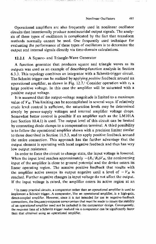
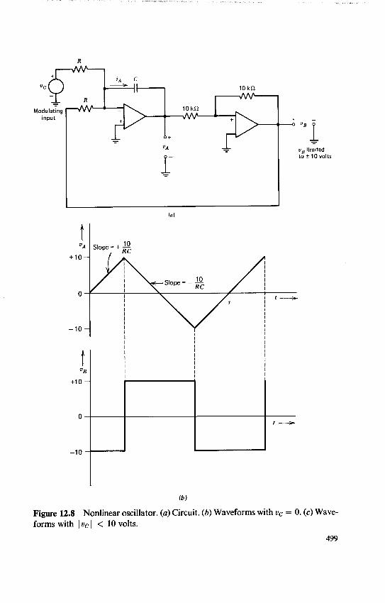
R
Vc
Modulating input
R1
+Ak-
VA
2
-to
10 kE2
++V
- o limited 10 volIts
VA Slope=+
+10 -
(a)
VBI 1
-10 -
t Soe
(b)
Figure 128 Nonlinear oscillator (a) Circuit (b) Waveforms with Vc = 0 (c) Waveshy
forms with IvcI lt 10 volts
499
500 Advanced Applications
vA Slop10 -VC
+10
Slope =-10 -VC
t
VB
+10
0 lt t-----gtshyt gt~
-10
(c)
Figure 128-Continued
In commercial versions of this circuit decade frequency switching is freshyquently accomplished by changing capacitors while variation of the value of resistor R provides vernier control in any one decade
1222 Duty-Cycle Modulation
The current that charges the capacitor can be modulated by means of an applied voltage vc with this current given by
VC + VB 1A = V + (1229)
R
A positive value for Vc increases capacitor charging current when VB is positive and decreases this current when VB is negative The net result is to
duty-cycle modulate the signal VB as shown in Fig 128c The fraction of the time this signal stays positive is
T+ __ =_20RC(lO + vc) I (I Vc(
7+ + 7- 20RC(1O + vc) + 20RC(1O - vc) 2 10
501 Nonlinear Oscillators
This duty-cycle modulator has a number of interesting features that make it useful in a variety of applications Equation 1230 shows that the duty cycle is linearly proportional to vc and changes from one to zero as Vc changes from - 10 volts to +10 volts However maximum capacitor charging current is limited to twice its value with zero vc so that the time spent in the shorter of the two periods is never less than half its quiescent value The frequency of operation is a nonlinear function of Vc and is given by
21 100 -Oc f =0=R= (1231)
r+ + T_ 20RC(10 + vc) + 20RC(10 - Vc) 400RC
This equation shows that the frequency is lowered by any nonzero value of Vc
Applications include the control of switching power amplifiers and the realization of the type of analog multiplier shown in Fig 129 In this circuit the duty-cycle modulator controls the state of a switch that is freshyquently realized with field-effect transistors The circuit is arranged so that the switch arm is connected to a voltage +vy for a fraction of the time
I[1 + (vxVR)] and to a voltage - vy for the remainder of the time a fraction equal to 1[1 - (vx VR)] (Alternative implementations use current rather than voltage switching to increase switching speed) The output filter (usually a multiple-order active filter rather than the simple network shown) averages the switch voltage vs so that
vo= s = +Vy [ + -Xy - (1232)
where the over bar indicates time averaging Note that the voltage VR
(which is equal to the maximum magnitude of the signal out of the Schmitt
+Vy
Fraction of time switch arm is high
is- (1 + )2 VR
Duty -cycle +Vmodulator
Duty cycle Vs_(1+LX T +T_ 2 VR
_VY
Figure 129 Time-division multiplier
502 Advanced Applications
trigger) can be varied to mechanize division A technique for varying the signal from the Schmitt trigger is described below
Versions of this type of multiplier that limit errors to 005 of maximum output have been designed
1223 Frequency Modulation
Another variation of the basic nonlinear oscillator shown in Fig 1210 results in an oscillator with a voltage-controlled operating frequency Here the Schmitt trigger determines the state of a switch that allows a variable-level voltage to be applied to the integrator If the Schmitt trigger switches at input-signal levels of d VT the total excursion of the signal VA will be 4 VT volts per cycle The slope of signal VA has a magnitude of VFRC volts per second and thus the frequency of oscillation is
VFRC _VF
=FR Vf = - (1233)4VT 4VTRC
1224 A Single-Amplifier Nonlinear Oscillator
The operational amplifier used as an integrator in the nonlinear oscillator described above can be replaced with a passive resistor-capacitor network a shown in Fig 1211 resulting in a configuration first reported by Bose2
The Schmitt trigger functions in an inverting mode in this connection so that a sufficiently positive level for vA saturates the amplifier output at - VM Switching points occur at VA = -[- VM R1(R 1 + R 2) If the dotted modulating resistor is omitted the waveforms are as shown in Fig 121 lc The capacitor voltage is a sequence of exponential segments rather than a true triangular wave The duty cycle of the signal can be modulated by including the dotted resistor shown in Fig 121la If the width of the hysterisis region is made very small by choosing R1 ltlt R2 the current into the capacitor becomes nearly constant in each state since the circuit keeps the capacitor voltage close to zero In this case the duty cycle of the voltage vo is linearly related to control voltage vC
123 ANALOG COMPUTATION
It was mentioned in Chapter 1 that operational amplifiers were initially used primarily for analog computation The objective in analog computashytion is to build an electrical network using operational amplifiers and
2 A G Bose A Two-State Modulation System 1963 Wescon Convention Record Part 6 Paper 71
C
0 VB (a)
VA
+ VT
Slope= shy
t -
Slope= +C
-- VT shy
VB
VF
- VF 4VTRC
VF
(b)
Figure 1210 Voltage-controlled oscillator (a) Circuit (b) Waveforms
503
504 Advanced Applications
R R
+jVC I
-T
VA~I -0
R2
vK01
Limited to plusmn VM
(a)
t Vo
S+ VM
+V R1 R
1 +R 2
VA gt
Figure 1211 One amplifier nonlinear oscillator (a) Circuit (b) Inverting Schmittshytrigger characteristics (c) Waveforms
associated components that obeys the same differential equation as does the system under study The answers obtained consist of the responses of the electrical analog to particular inputs and initial conditions
Analog computers are available from several manufacturers These machines incorporate in addition to the necessary hardware a considerable human-engineering effort Summing amplifiers and integrators included in these machines are normally constructed with fixed scale factors so that external components need not be used For example several inputs with gains of - 1 and - 10 are typically provided for each summing amplifier
505
V
Analog Computation
Toward +VM with time constant RC+yMn
R +R2 V
tshy
-VM time constant R C
+VMv0
0- t -shy
(c)
Figure 1211-Continued
Potentiometers are also included and these devices are combined with
fixed-gain amplifiers to provide arbitrary gain levels Thus a gain of -312
might be realized by preceding a gain of - 10 amplifier with a potentiometer
set for an attenuation of 0312 Nonlinear elements such as function genshy
erators and multipliers are frequently included The inputs and outputs of
the various elements are usually connected to jacks of some type The intershy
connections necessary to simulate a particular system are then made with
patchcords that connect the various jacks In many cases the programming
(inserting the patchcords to establish the proper connection pattern) is
done on a board physically removed from the computer while other users
with their own boards solve their problems The board makes the required
connections when it is inserted into a mating plate located on the machine
While the accuracy of solutions obtained via analog computation is limited by component tolerances it normally far exceeds the accuracy required
for the simulation of physical systems which are themselves constructed
with imprecise components A further consideration is that it is frequently
506 Advanced Applications
possible to get a good physical feeling for a system via analog computation since many variables are available for observation and since the effects of parameter variations can be quickly investigated
Our treatment here can only cover the barest essentials and highlight a few of the ancillary circuits that were evolved for analog computation The reader interested in a detailed treatment of this fascinating and powerful technique is referred to Korn and Korn
1231 The Approach
Our objective here is to show how electronic-analog techniques are used to simulate differential equations that describe the systems to be studied We initially assume that the differential equation under investigation is linear and has the general form
d~x -x dx an dtx + a-1 dt-x + - + ai - + aox = f(t) (1234)dtn r- dt
It is certainly not necessary that the independent variable of the system under study be time as implied by Eqn 1234 For example if we were investigating the deflection of a bridge under static load we might be interested in vertical displacements from equilibrium as a function of disshytance from one end of the bridge However since our analog will use time as its independent variable we substitute time for the independent variable if necessary in the original equation Similarly we realize that any dependent variables in our analog will have to be voltages regardless of the variables they actually represent in the system under study
Equation 1234 is rewritten so that the highest derivative of x is expressed in terms of the other variables in the form
dx an_ 1 d- 1 x a1 dx aox 1 dtn andt~ dt-~ 1
- a~ d a~ + - f(t) (1235)dt--1 an dt an an
Equation 1235 can be represented as the block diagram shown in Fig 1212 In this representation the variable dnxdtn appears as the output of a summation point Inputs to the summation point are scaled multiples of the driving function and the lower-order derivatives of x The lower-order derivatives are obtained by successive integrations of dnxdtn with a total of n integrations required to complete the block diagram
Note that the only elements included in the block diagram are a multiple-input summation point inverters to precede some inputs on the summer
I G A Korn and T M Korn Electronic Analog and Hybrid Computers 2nd Edition McGraw-Hill New York 1972
f (t)
Figure 1212 Block diagram of Eqn 1235
(I
508 Advanced Applications
gain blocks and integrators Since each of these elements can be readily constructed using operational amplifiers and passive components the block diagram can be implemented using these devices When the analog realizashytion is excited with a voltage equal tof(t) voltages equal in value to x and its derivatives will be available as the outputs of the integrators
As an example of this process consider the differential equation
dex d3x d2x dx - + 261 d + 342 d2 + 261 + x = f(t) (1236)dt4 dt dts dt
(We recall from Section 332 that this equation represents a fourth-order Butterworth filter) Solving for d 4xdt yields
dex d3x d2x dx -= -261 - 342 - - 261 - x + f(t) (1237)
dt4 dt3 dt2 dt
One possible simulation of this equation is shown in Fig 1213 The voltages expected at the output of various amplifiers are indicated by writing the value of the variable the voltage represents at appropriate nodes Note that in contrast to traditional analog-computer methods gains are established by selecting impedances 4 used around operational amplifiers rather than by combining potentiometers with fixed-gain amplifiers and integrators Also functions have been combined in order to reduce the number of amplifiers required The use of inverting connections only is traditional in analog computation and reflects that fact that an operashytional-amplifier design technique frequently used to improve d-c performshyance results in an amplifier that can only be used in inverting connections (See Section 1233) It may of course be possible to use noninverting integrators or summing amplifiers (realized with resistive summing at the input to a noninverting-amplifier connection) if general-purpose operashytional amplifiers are used for this simulation
The four integrators appear along the top of the diagram Since it is assumed that there is no need to have a voltage representing d 4xdt4 availshyable the summing operation is included in the first integrator connection The output of this integrator is - (dlxdt) when the indicated current is equal to (10-6 A) d 4xdt4 Since inverting integrators are used the signs associated with successive derivatives alternate The scaling and inversions required by the coefficients of x and its second derivative are obtained with the bottom amplifier
4The relative impedance levels shown in Fig 1213 are high if general-purpose operashytional amplifiers such as the LM101A are used Since only ratios are important in estabshylishing the transfer function all impedance levels can be scaled to reduce errors that result from amplifier input currents
Current here equals 1pF
(10-6 A) 4xdt47 1 pF
1 pF 1 M F
1pF
1 M261
1 M92
1 M92
M32
1 ME2
Figure 1213
-x -342 d dt
2
Simulation of fourth-order Butterworth equation
510 Advanced Applications
The number of amplifiers required in Fig 1213 indicates the general rule If this topology is used simulating an nth-order linear differential equation requires n integrators and one amplifier that inverts appropriate signals as necessary to complete feedback paths
Analog-computing techniques can also be used to solve a variety of nonshylinear differential equations by including hardware that implements the nonlinearity in the simulation As an example consider Van der Pols differential equation
dsx dx + y(x 2 - 1) + x = 0 (1238)
dt2 dt
where y is a positive constant For small values of x the coefficient of the first derivative term is negashy
tive and increasing-amplitude oscillations result When the amplitude of the oscillation becomes large enough the coefficient of the first derivative will be positive over part of the cycle and a limit cycle can result Equation 1238 is rewritten in a form convenient for simulation as
d 2 x dx dx = - - x (1239)
dtz dt dt
2Multipliers are required to generate x and form the x 2(dxdt) product necessary for the simulation of Eqn 1239 Two techniques for analog multiplication were described in Sections 1155 and 1222 Practical multishypliers based on these methods are often designed to have an output voltage equal to the product of the two input voltages divided by 10 volts for comshypatibility with the dynamic range of most solid-state operational amplifiers Figure 1214 shows a possible simulation of Eqn 1239 assuming that multipliers with this scale factor are used
Van der Pols equation is an example of an undriven differential equashytion and excitation is by initial conditions only While initial conditions were not mentioned in our earlier discussion of the simulation of linear differential equations we recognize that we must specify n initial conditions in order to determine the complete (homogeneous plus driven) solution of an nth-order differential equation These initial conditions can be set simply by establishing the voltages on the integrating capacitors at time t = 0 since these voltages are proportional to the values of x and its first n - I derivatives A circuit for setting initial conditions is described in Section 1233
The value of x as a function of time for Van der Pols equation with y = 025 is shown in Fig 1215 The initial conditions used for parts a and b of this figure are x(0) = 05 (dxdt)(0) = 0 and x(0) = 3 (dxdt)(0) = 0 respectively We see that in both cases the amplitude of the limit cycle conshy
511 Analog Computation
1 MG
- x 2 dx if x2
1 Mn 10_0 dt 10 IE Multiplier - - -- Multiplier
_1 1 Mamp2
Figure 1214 Simulation of Van der Pols equation
verges to a peak-to-peak value of approximately 4 Part c of this figure is a plot of dxdt versus x(t) This representation in which time is a parameter
along the curve is called a phase-plane plot The responses for both values
of initial conditions are included The convergence to equal-amplitude
limit-cycles for both sets of initial conditions is evident in this figure
The formal procedure described here is certainly not the only one which
results in a correct analog representation of a problem While it does lead
to a compact realization other realizations may maintain better correshy
spondence with the physical system that is being modeled One popular
alternative technique involves simply drawing a block diagram for the
system under study and then implementing the block diagram on a blockshy
by-block basis without ever writing down the complete system differential
equation While this approach often requires more hardware to complete
the simulation it is convenient in that voltages proportional to the actual
variables of interest in the problem under study are avaliable Furthermore it is generally possible using this alternative to associate scale factors with
the parameters of physical elements in the simulated systems on a one-toshy
one basis
x(t) 2 shy
0 020 t 30 (seconds)
-2shy(a)
4shy
t x(t)
2 shy
0__ 010 20 t 30
- v Y v(seconds)
-2 -
(b)
-4 shy
Figure 1215 Solution to d2xdt
2 + 025(x 2 - 1)(dx dt) + x = 0 (a) With initial
conditions x(0) = 05 (dx dt)(0) = 0 (b) With initial conditions x(0) = 3 (dx dt)(0) = 0 (c) Parts a and b repeated in phase-plane form
512
513 Analog Computation
I dx dt
x=3 dX 0dt
-5 x(t)
Direction of increasingtime
-4 Lshy
(c)
Figure 1215-Continued
1232 Amplitude and Time Scaling
Practical considerations constrain the amplitude and frequency range of the signals that arise in analog computation We normally prefer maxishymum signal levels that are comfortably below amplifier saturation levels but well above noise and offset uncertainties Similarly very low-frequency signals are difficult to integrate accurately while the limited gain of an operational amplifier at high frequencies compromises accuracy in this frequency range Amplitude scaling and time scaling are used to standardize signals to convenient amplitude levels and spectral content
Amplitude scaling involves little more than some additional bookkeeping effort Since we are using voltages for all of the dependent variables in our simulation there must be a dimensioned scale factor that relates the mashychine variables to the problem variables when the problem variables are quantities other than voltages For example if x is a displacement in meters and some voltage in a simulation represents this variable on a 1 meter = 1 volt basis the machine variable should really be labeled (1 voltmeter)x rather than simply x as is frequently done We should realize that the number associated with the scale factor can readily be selected to be other than unity Thus we might use lOx as the label for some voltage or preferably (10 voltsmeter)x If this voltage were 7 volts the correshysponding displacement would be x = (7 volts) (1 meter 10 volts) = 07 meter The appropriate values for scale factors can only be determined with a knowledge of approximate problem-variable levels since the correspondshying machine variables should have peak values slightly below the saturation
514 Advanced Applications
level Once scale factors have been selected they are implemented by modishyfying the gains of amplifiers and integrators from their initially selected values
Time scaling has advantages beyond those of centering signal-frequency components within the range of optimum operational-amplifier performshyance Consider for example the simulation of a planetary motion problem that may require years of real time to complete Using a faster machine time scale permits us to obtain the solution in a more reasonable time interval Similarly the use of a slower than real time scaling procedure allows us to display the buildup of charge in the base region of a transistor at a rate comfortable for viewing on a display oscilloscope
The technique used for time scaling involves the substitution
t = or (1240)
where r is machine time and is equal to real time divided by a scale factor 0 A value of a-greater than one implies that the machine solution is faster than the actual solution so that one second of real time is represented by a shorter period r of machine time
This process is illustrated using the form for a differential equation given in Eqn 1234 and repeated here for convenience
dux ux dx an dt + an_1 dtx + + a dt + aox = f(t) (1234)
dtn dr-1dt
In order to apply the substitution of Eqn 1240 we change f(t) tof(-r) and change dmxdtm to (lum)(dxdrm) Thus the time-scaled version of Eqn 1234 is
an dax an_1 dux dxa1 - d+xplusmn d + -lx plusmn- + aox = f(r) (1241) e-ndr an- 1 dr- o dr
The equation when simulated will have a solution identical in form to that of Eqn 1234 but will run a factor of a-faster than the original equation
A second way to implement time scaling is to realize that the dynamics of the simulation are implemented by means of integrations and that changshying the scale factor of every integrator in the simulation by some factor must change the time scale of the simulation by precisely the same factor Thus problems can be time scaled by first simulating the problem for a
real-time solution and then dividing the value of every capacitor by a
factor of a Alternatively every resistor used to implement all integrators can be reduced in value by a factor of a or the scale-factor change can be apportioned between resistors and capacitors The net result of any of these modifications will be to make the problem on the machine run a factor ofa faster than the real-time solution It is of course still necessary to increase the speed of driving functions applied to the system by a factor of a if these
515 Analog Computation
signals are derived from sources that are not implemented using scaled integrators
The coefficients of the original differential equation often can be used to determine the time scale appropriate to a particular problem If the roots of the characteristic equation have approximately equal magnitudes the natural frequencies of the undriven solution will be the order of
w - (1242)(a Conversely if the system is dominated by one pole the characteristic freshyquency is the order of
ao (1243) ai
The characteristic frequencies given by Eqn 1242 or 1243 can be changed to values convenient for display and compatible with operational-amplifier performance by appropriate selection of a
The element values that occur in a problem simulation often provide clear indications of the need to modify amplitude or time scales If for example we find that high gain is required at the input of every amplifier being supplied with some particular signal the scale factor of that signal is probably too small relative to other amplitude scale factors used Simishylarly if one input resistor to a summing amplifier or an integrator is much larger than all other input resistors associated with the amplifier the implication is that the term applied to the input in question contributes little to the output of the summer or integrator In the case of time-scale selection an inappropriate choice is usually reflected by unreasonable resistor values capacitor values or both associated with integrators
The Van der Pol equation simulated earlier (Eqn 1238) is used as a simple example of time and amplitude scaling For the range of initial conditions used previously and with A = 025 the maximum magnitudes of x and dxdt are approximately 3 and 3 sec-1 respectively while the maximum magnitude of d 2xdt2 is slightly greater than 3 sec-2 Accordshy
ingly if 10-volt maximum amplifier outputs are assumed scale factors of 3 volts per unit for x and dxdt combined with a scale factor of 2 volts per unit for d 2xdt2 are reasonable If Eqn 1239 is rewritten using these scale factors we obtain
d2x 2 dx 2 dx 2
2 -= - y(3x)2 3 + - 3- - (3x) (1244)dt2 27 dt 3 dt 3
The simulation diagram again assuming that multipliers with outputs equal to the product of the inputs divided by 10 are used is shown in Fig 1216 It has also been assumed in forming this diagram that a voltage
516 Advanced Applications
proportional to d2xdt2 is required Note that the input signals applied to the first amplifier are negatives of the right-hand side of Eqn 1244 because of the inversion associated with this amplifier The transfer funcshytion of the first integrator is -(32s) so that it provides an output of -3(dxdt) when driven with 2(d 2xdt2) Alternate scaling may be advanshytageous if different values of y are used to keep the maximum magnitudes of the voltages proportional to dxdt and d 2xdt2 at optimum levels
If a value of RC = 1 second is used the solution will run at real time and the oscillation frequency will be about one radian per second Changing this product will time scale the solution For example the use of RC = 1 ms results in limit-cycle oscillation at approximately 1000 radians per second
1233 Ancillary Circuits
There are several interesting circuit configurations that are frequently employed in analog computation and that also can be used in other more general applications
One of these topologies is the three-mode integrator We have seen that it is necessary to apply initial conditions to integrators in order to obtain complete (homogeneous plus driven) solutions for simulated differential
1MG C
C
2 X dt2 -3 yx
dt
3 + R 3
Figure 1216 Scaled simulation of Van der Pols equation
517 Analog Computation
equations Another useful computing mode results if all integrators are simultaneously switched to a state where their outputs become time inshyvariant and thus hold the values that were present at the switching time The values of problem variables at the switching time can then be detershymined accurately with a digital voltmeter
The three-mode integrator shown in Fig 1217 permits application of initial conditions and allows holding an output voltage in addition to functioning as an integrator The reset (or initial condition) operate and hold modes are selected by appropriate choice of switch positions With switch D open and switch o closed the amplifier closed-loop transfer function is
V0(s) __ 1 V(S) RC(1245) V-(s) R2Cs + 1
If VA is time invariant in this mode the capacitor will charge so that the output voltage eventually becomes the negative of VA The capacitor voltage can then provide initial conditions for subsequent operations
If switch o is closed and switch o is open the amplifier integrates VB in the usual fashion
With both switches open capacitor current is limited to operational-amplifier input current and capacitor self-leakage thus capacitor voltage is ideally time invariant
C
R||
VB
R2 R2
VA
Figure 1217 Three-mode integrator
518 Advanced Applications
The required reset time of the connection shown in Fig 1217 can be quite long if reasonable values are used for the resistors labeled R2 The use of a second operational amplifier connected as a voltage follower and supplying a low-resistance drive for the inverting input of the integrator can substantially shorten reset times A practical three-mode integrator circuit that incorporates this feature is shown in Fig 1218
The bipolar-transistor drivers are compatible with T2L logic signals and drive the gate potential of field-effect-transistor switches to ground on inputs that exceed two diode forward voltages With a high level for the operate signal and the reset signal at ground Q1 is on and Q2 is off This combination puts the circuit in the normal integrating mode FET Qi has a drain-to-source on resistance of approximately 25 ohms and this value is compensated for by reducing the integrating-resistor size by a
+15V +15V +15V
10 kE2
Reseton high
-15 V
Input to be Q1 2N4391 integrated
Output
Initial-condition input
Figure 1218 Circuit for three-mode integrator
519 Analog Computation
corresponding amount Diode D1 does not conduct significant current in this state Diodes D2 and D3 keep the output of the follower within approxishymately 06 volt of ground One benefit of this clamping is that the source of Q2 cannot become negative enough to initiate conduction with its gate at - 15 volts since the maximum pinchoff voltage of the 2N4391 is 10 volts Clamping the follower input level also keeps its signal levels near those anticipated during reset thus avoiding long slewing periods when the circuit is switched to apply initial conditions
With the gate of Q1 at - 15 volts (corresponding to a low level on the operate control line) diode D1 prevents source potentials that would initiate conduction of transistor Q1 If Q2 is on the output voltage is driven toward the negative of the initial-condition input-signal level The details of the transient for a large error depend on diode FET and amplifier characteristics As the error signal becomes smaller the reset loop enters its linear operating region The reader should convince himself that the linear-region transmission of the reset loop (assuming ideal operational amplifiers) is - l2rdCs where rd is the incremental drain-to-source on resistance of the FET Thus the low FET resistance rather than R2 detershymines linear-region dynamics
The hold mode results with both the operate and the reset signals at ground so that both FETs are off In this state the current supplied to the capacitor is determined by FET leakage and amplifier input current
One application for this type of circuit in addition to its use in analog computation is as a sample-and-hold circuit In this case the operate switch is not needed and the circuit is switched from sampling the negative of an input voltage to hold with Q2
Sinusoidal signals are frequently used as test inputs in analog-computer simulations A quadrature oscillator that includes limiting and that is easily assembled using components available on most analog computers is shown in Fig 1219 The diagram implies a simulated differential equation prior to limiting of
- 2 C2 d RCdv + v0 (1246) dt2 K dt
We recognize this equation as a linear second-order differential equation with c = 1RC and = - 12K The value of K is chosen small enough
to guarantee oscillation with anticipated capacitor losses and amplifier imperfections thus insuring that signal amplitudes will be determined primarily by the diode-resistor networks shown
A precisely known voltage reference is required in many simulations to apply constant input signals provide initial-condition voltages function as a bias level for nonlinearities or for other purposes Voltage references are also used regularly in a host of applications unrelated to analog simulation
R2 R2
C R3 R3
R
RRCdt R
RIR
-RCC
dR
Figure 1219 Quadrature oscillator with limiting
521 Analog Computation
The circuit shown in Fig 1220 is a simple yet highly stable voltage refershyence The operational amplifier is connected for a noninverting gain of slightly more than 15 so that a 10-volt output results with 64 volts applied to the noninverting amplifier input
With the topology as shown the voltage across the resistor connected from the amplifier output to its noninverting input is constrained by the amplifier closed-loop gain to be 0562 Vz where Vz is the forward voltage of the Zener diode The current through this resister is the bias current apshyplied to the Zener diode Zener-diode current is thus established by the stable value of the Zener voltage itself The Zener output resistance does not deteriorate voltage regulation since the diode is operated at constant current in this connection The filter following the Zener diode helps to attentuate noise fluctuations in its output voltage
An emitter follower is included inside the operational-amplifier loop to increase output current capacity (current limiting circuitry as discussed in Section 84 is often a worthwhile precaution) and to lower output impedshyance particularly at higher frequencies While the low-frequency output impedance of the circuit would be small even without the follower because of feedback this impedance would increase to the amplifier open-loop output impedance at frequencies above crossover The emitter follower reduces open-loop output impedance to improve performance when pulsed or high-frequency load-current changes are anticipated A shunt capacitor at the output may also be used to lower high-frequency output impedance (See Section 522)
Start-up diode
V +5 V
64 V
Temperature shycompensated 0562 R1 Zener diode
Trim to -adjust output
voltage
Figure 1220 Voltage reference
522 Advanced Applications
The bootstrapping used to excite the Zener diode is of course a form of positive feedback and would deteriorate performance if the magnitude of this feedback approached unity The low-frequency transmission of the positive feedback loop is
L = 1562 rd - (1247)R + rd
where rd is the incremental resistance of the Zener diode This expression is evaluated using parameters for a 1N829A a temperature-compensated Zener diode The diode is designed for an operating current of 75 mA and thus R will be approximately 500 Q The incremental resistance of the diode is specified as a maximum of 10 Q Thus the loop transmission is from Eqn 1247 003 This small amount of positive feedback does not significantly affect performance
The positive feedback can result in the circuit operating with the diode in its forward-conducting state rather than its normal reverse-breakdown mode This state which leads to a negative output of approximately one volt can be eliminated with the start-up diode shown The start-up diode insures that the Zener diode is forced into its reverse region but does not contribute to Zener current under normal operating conditions
The expected operational-amplifier imperfections have relatively little effect on the overall performance of the reference circuit A value of 30000 for supply-voltage rejection ratio (typical for integrated-circuit amplifiers) causes a change in output voltage of approximately 50 AV per volt of supply change (This 33 yVV sensitivity is amplified by the closed-loop gain of 15) The typical input-voltage drift for many inexpensive operashytional amplifiers is the order of 5 MV per degree Centigrade This figure is not significant compared to the temperature coefficient of 5 parts per million per degree Centigrade or approximately 32 MV per degree Centishygrade of a high-quality Zener diode such as the 1N829A
The designers of the large analog computers that evolved during the period from the early 1950s to the mid-1960s often devoted almost fanatical effort to achieving high static accuracy in their computing elements Toward this end operational amplifiers were surrounded with high-precision wire-wound resistors and capacitors that could be accurately trimmed to desired values These passive components were often placed in temperature-stable ovens to eliminate variations with ambient temperature
The low-frequency errors (particularly input voltage offset) characteristic of vacuum-tube operational amplifiers were largely eliminated by means of an imaginative technique known as chopper stabilization5 This method
IE A Goldberg Stabilization of Wide-Band Direct Current Amplifiers for Zero and Gain RCA Review Vol II No 2 June 1950 pp 296-300
Figure 1221 Chopper-stabilized amplifier
LA
524 Advanced Applications
is still incorporated into some modern operational-amplifier designs and it provides a way of reducing the voltage drift and input current of an amplifier to vanishingly small levels The usual implementation of this technique can be viewed as an extreme example of feedforward (see Section 822) and thus results in an amplifier that can only be used in inverting connections
Figure 1221 illustrates the concept Assume that the optional network is eliminated so that the junction of Zf and Z is connected directly to the inverting input of the top amplifier The resulting connection clearly funcshytions as an inverting amplifier if the voltage vc is zero Observe that one necessary condition for the amplifier closed-loop gain to be equal to its ideal value is that VA = 0 The objective of chopper stabilization is to reduce VA to nearly zero by applying an appropriate signal to the non-inverting input of the top amplifier
The d-c component of the voltage VA is determined with a low-pass filter and this component (VB) is chopped (converted to a square wave with peak-to-peak amplitude VB) using a periodically operated switch (Early designs used vibrating-reed mechanical switches while more modern units often use periodically illuminated photoresistors or field-effect transistors as the switch) The chopped a-c signal can be amplified without offset by an a-c amplifier and demodulated to produce a signal yc proportional to VB If the gain of the a-c amplifier is high the low-frequency gain VCVA = a0 2
will be high If a02 is negative the signal applied to the positive gain input of the top amplifier will be of the correct polarity to drive VA toward zero Arbitrarily small d-c components of VA can theoretically be obtained by having a sufficiently high magnitude for a02 although in practice achievable offsets are limited by errors such as thermally induced voltages in the switch itself The low-pass filter is necessary to prevent sampling errors that arise if signals in excess of half the chopping frequency are applied to the chopper
An alternative way to view the operation of a chopper-stabilized amplifier is to notice that high-frequency signals pass directly through the top amplishyfier while components below the cutoff frequency of the low-pass filter are amplified by both the bottom amplifier and the top amplifier in cascade (It is interesting to observe that low-frequency open-loop gain magnitudes in excess of 10 have been achieved in this way) It is therefore not necessary to apply low-frequency signals directly to the top amplifier and a high-pass filter (shown as the optional network) can be included in series with the inverting input of the top amplifier As a result both voltage offset and input current to the operational amplifier can be reduced by chopper stabilization yielding an amplifier with virtually ideal low-frequency characteristics
Several manufacturers offer packages that combine discrete-component choppers with integrated-circuit amplifiers More recently integratedshy
525 Active Filters
C1 v
Figure 1222 Second-order low-pass active filter
circuit manufacturers have been able to fabricate complete chopper-stabilized amplifiers either in monolothic form or by combining several monolithic chips to form a hybrid circuit These circuits incorporate topological improvements that permit true differential operation The large capacitors required are connected externally to the package Drifts of a fraction of a microvolt per degree Centigrade coupled with input currents in the picoampere range are available at surprisingly low cost
124 ACTIVE FILTERS There are numerous applications that require the realization of a particushy
lar transfer function One of the many limitations of the design of filter networks using only passive components is that inductors are required to obtain complex pole locations This restriction is removed if active elements are included in the designs and the resultant activefilterspermit the realizashy
tion of complex poles using only resistors and capacitors in addition to the active elements Further advantages of active-filter synthesis include the possibility of a wide range of relative input and output impedances and the use of smaller less expensive reactive components than is normally possible with passive designs
There is a fair amount of present research devoted toward improving techniques for active-filter synthesis and the probability is that better deshysigns particularly with respect to sensitivity (the dependence of the transfer function on variations in parameter values) will evolve This section deshyscribes two presently popular topologies that can be used to realize active filters
1241 The Sallen and Key Circuit6
Figure 1222 shows an active-filter circuit that uses a unity-gain-conshynected operational amplifier Node equations for the circuit are easily
I R P Sallen and E L Key A Practical Method of Designing RC Active Filters Instishytute of Radio Engineers Transactions on Circuit Theory March 1955 pp 74-85
526 Advanced Applications
written by noting that the voltage at the noninverting input of the amplifier is equal to the output voltage and are
G1Vi =(G 1 + G2 + C2s)V - (G2 + C2 s)Vo (1248)
0 = -G 2 V + (G2 + C1s)V
Solving for the transfer function yields
V0(s) 1V(S shyCC2S2(1249)
Vi(s) R1 R 2C1 C2s2 + (R 1 + R2 )Cls + 1
This equation represents a second-order transfer function with standard-form parameters
n VR 1R2C1C2 (1250)
and
R1 + R 2 (1251)
2VR 1 R 2 C2
Since only two quantities are required to characterize the second-order filter the four degrees of freedom represented by the four passive-comshyponent values are redundant Part of this redundancy is frequently elimishynated by choosing R1 = R2 = R In this case the standard-form paramshyeters become
on (1252)R -C1C2
and
= (1253)
The addition of another section to the second-order low-pass active filter as shown in Fig 1223 allows the synthesis of a third-order transfer function with a single amplifier If equal-value resistors are used as shown the transfer function is
V 0(s) _ _____1________ V-(S - I 2S2(1254)
C1C2 2 (C1Vi(s) C3 Rs 3 + 2(C 1C3 + C2C3)R2s + + 3C3)Rs + 1
An nth-order low-pass filter is often designed by combining n2 second-order sections in the case of n even or one third-order section with n2 - 32 second-order sections when n is odd Tables7 that simplify
I Farouk Al-Nasser Tables Speed Design of Low-Pass Active Filters EDN March 15 1971 pp 23-32
527 Active Filters
C2
R R R
Figure 1223 Third-order low-pass active filter
element-value selection are available for filters up to the tenth order with a number of different pole patterns
Interchanging resistors and capacitors as shown in Fig 1224 changes the second-order low-pass filter to a high-pass filter The transfer function for this configuration is
2Vo(s) _ R1 R 2C1C 2s
Vi(s) R1R2C1C2s2 + R2(C1 + C2)s + 1
If in a development analogous to that used for the low-pass filter we choose C1 = C2 = C Eqn 1255 reduces to
V 0(s) s2_____________2 _
V-(S S2 W2(1256) V1(s) (s2 2) + (2 so) + 1
where
I
CVR1 R 2 and
R2
R 1
R2
Cy C2
7 ++
+iR -V 0~-1
Figure 1224 Second-order high-pass active filter
528 Advanced Applications
The Sallen and Key circuit can be designed with an amplifier gain other than unity (see Problem P128) This modification allows greater flexibility since the low- or high-frequency gain of the circuit can be made other than one However the damping ratio of transfer functions realized in this way is dependent on the values of resistors that set the closed-loop amplifier gain thus poles may be somewhat less reliably located A further advantage of the unity-gain version is that it may be constructed using the LM 110 inteshygrated circuit (see Section 1044) The bandwidth of this amplifier far exceeds that of most general-purpose integrated-circuit units and corner frequencies in the low megahertz range can be obtained using it
1242 A General Synthesis Procedure
The Sallen and Key configuration together with many other active-filter topologies allows-complete freedom in the choice of pole location but does not permit arbitrary placement of transfer-function zeros The application of the analog-computation concepts described in Section 1231 allows the synthesis of any realizable transfer function that is expressable as a ratio of polynomials in s provided that the number of poles is equal to or greater than the number of zeros in the transfer function
Consider the transfer function
V(s) _ b s + bn_1 s-1 + - + b1s + bo (1257) Vi(s) as + ans 1 + - + ais + ao
The first step is to introduce an intermediate variable V(s) such that Vj(s) Vi(s) contains only the poles of the transfer function or
Va(S) 1(1258)Vi(s) ans + a_s--1 + + ais + ao
Proceeding in a way exactly parallel to the time-domain development of Section 1231 we write
SVa(S-(s) - -a s V(s) - ao Va(S) + Vi(s) (1259) a an an a
The block-diagram representation of Eqn 1259 is shown in Fig 1225 This block diagram can be readily implemented using summers and inteshygrators In order to complete the synthesis of our transfer function (Eqn 1257) we recognize that
V(s) = Va(s) (b s + bs-- + - + bis + bo) (1260)
The essential feature of Eqn 1260 is that it indicates V(s) is a linear comshybination of Va(s) and its first n derivatives Since all of the necessary varishy
Figure 1225 Block diagram representation of transfer function that contains only poles
LAi
530 Advanced Applications
ables appear in the block diagram V(s) can be generated by simply scaling and summing these variables without the need for differentiation
This synthesis procedure is illustrated for an approximation to a pure time delay known as the Pad6 approximate The time delay has a transfer function e-1 where r is the length of the delay The magnitude of this transshyfer function is one at all frequencies while its negative phase shift is linearly proportional to frequency The time delay has an essential singularity at the origin and thus cannot be exactly represented as a ratio of polynomials in s
The Taylors series expansion of e- 7 is
s22 SmnTm e- = 1 - sr + - + - - - + (-1) + - (1261)
2 M
The Pade approximates locate an equal number of poles and zeros so as to agree with the maximum possible number of terms of the Taylors series expansion This approximation always leads to an all-pass network that has right-half-plane zeros and left-half-plane poles located symmetrically with respect to the imaginary axis This type of singularity pattern results in a frequency-independent magnitude for the transfer function
Since we can always frequency or time scale at a later point we consider a unit time delay e- to simplify the development The first-order Padd approximate to this function is
I - (s2) s2 s 3
= 1-splusmn - +-- + - + (1262)1 + (s2) 2 4
The expansion for e- is
2 5 s s3 s4 s s6
e-= 1- s +-- + + - + (1263)2 6 24 120 720
The first-order approximation matches the first two coefficients of s of the complete expansion and is in reasonable agreement with the third coefficient This match is all that can be expected since only two degrees of freedom (the location of the pole and the location of the zero) are available for the first-order approximation The second-order Pad6 approximate to a one-second time delay is
1 - (s2) + (s212)
1 + (s2) + (S212)
s4S2 s 3 s5
-s+ + - - - - ---+ (1264)2 6 24 144
531 Active Filters
x0
s plane
X 0
Figure 1226 Singularity locations for second-order Pade approximate to one-
second time delay
As expected the first four time-delay coefficients of s are matched by the
approximation The s-plane plot for P 2(s) is shown in Fig 1226 Simple
vector manipulations confirm the fact that the magnitude of this function
is one at all frequencies The phase shift of the approximating function is (from Eqn 1264)
4 P2(jo) = 2 4 1 - + (I] 2 tan- 1 2 [1 - C212)] (1265)
This function is compared with an angle of - 573cr (the value for a one-
second time delay) in Fig 1227 We note excellent agreement to frequencies
of approximately 2 radians per second implying that the approximation
represents the actual function well for sinusoidal excitation to this freshy
quency with increasing discrepancy at higher frequencies The error reshy
flects the fact that the maximum negative phase shift of the Pad6 approxishy
mate is 360 while the time delay provides unlimited negative phase shift
at sufficiently high frequency
Synthesis is initiated by defining an intermediate variable Va(s) in accordshy
ance with Eqns 1258 and 1259 or
V-(s) -1 (1266)V(s) (s212) + (s2) + 1
and
S2 Va(S) = -- 6sVa(s) - 12 V(s) + 12Vi(s) (1267)
532 Advanced Applications
o (radsec) -3
4 5 6 7 8 90 1 2 3
-900
Phase shift of second-order Pade approximate to one-second
-180- time delay
t Phase shift of
-270 - one-second time delay
-360 shy
-450shy
-540shy
Figure 1227 Comparison of time delay and Pad6 approximate phase characteristics
The output voltage is
S2 s V0(s) - V(S) - - Va(S) + Va(S) (1268)
12 2
The operational-amplifier synthesis shown in Fig 1228 provides the required transfer function if RC = 1 second The reader should convince himself that the liberties taken with inversions and various resistor values do in fact lead to the desired relationship
Anticipated amplitudes depend on the input-signal level and its spectral content For example if a step is applied to the input of the circuit the magnitude of the signal out of the first amplifier must initially be 12 times as large as the step amplitude since the outputs of the integrators cannot change instantaneously to subtract from the input-signal level Note howshyever that the input-to-output transfer function of the circuit remains the same for any values of R1 = R2 If for example 10-V step changes are expected at the input selection of R1 = R2 = 120 kQ will limit the signal level at the output of the first amplifier to 10 volts while maintaining the correct input-to-output gain
The circuit shown in Fig 1228 was constructed using R = 100 kQ and C = 001 MF values resulting in an approximation to a 1-ms time delay This choice of time scale is convenient for oscilloscope presentation The
R2= 10 kE2
Vt -V
Y Y Y
A Figure 1228 Synthesis of second-order Pade approximate to a time delay
200 mV
I T
(a) 1 ms
200 mV
(b) 1 Ms
Figure 1229 Input and output signals for second-order Padd approximate to a 1-ms time delay (a) Sine-wave excitation (b) Triangular-wave excitation (c) Square-wave excitation
534
535 Active Filters
200 mV
I T
(c) 1 ms
Figure 1229-Continued
input and output signals for 100-Hz sine-wave excitation are shown in Fig 1229a The time delay between these two signals is 1 ms to within instrushymentation tolerances This performance reflects the prediction of Fig 1227 since good agreement to 2000 radsec or 300 Hz is anticipated for the apshyproximation to a 1-ms delay
Input and output signals for 100-Hz triangular-wave excitation are comshypared in Fig 1229b The triangular wave contains only odd harmonics and these harmonics fall off as the square of their frequency Thus the amplitude of the third harmonic of the triangular wave is approximately 11 of the amplitude of the fundamental the amplitude of the fifth harmonic is 4 of the fundamental while higher harmonics are further attentuated We notice that the circuit does very well in approximating a 1-ms time delay most of the time The aberration that results immediately following a change in slope reflects the inability of the circuit to provide proper phase shift to the higher-frequency components
The performance of the circuit when excited with an 100-Hz square wave is shown in Fig 1229c The relatively poorer behavior in the vicinity of a transition in this case results from the higher harmonic content of the square wave (Recall that the square wave contains odd harmonics that fall off only as the first power of the frequency)
536 Advanced Applications
125 FURTHER EXAMPLES
It was mentioned in the introduction to Chapter 11 that the objective of
the application portion of this book was to illustrate concepts for design
rather than to provide specific detailed examples in the usually futile
hope that the reader could apply them directly to his own problems
Successful design almost always involves combining bits and pieces a
concept here a topology there to ultimately arrive at the optimum solution
In this section we will see how some of the ideas introduced earlier are
combined into relatively more sophisticated configurations The three
examples that are presented are all real world in that they reflect actual
requirements that the author has encountered recently in his own work
1251 A Frequency-Independent Phase Shifter
There are a number of operational-amplifier connections such as the
approximation to a time delay described in the previous section that have
a transfer-function magnitude independent of frequency combined with
specified phase characteristics The phase shifter shown in Fig 1230 is
another example of this type of circuit We recognize this circuit as a differshy
ential-amplifier connection and thus realize that its transfer function is
V__s = 2RCsRs-1V0(s) = _2RC - 1 = RCs -1 (1269) Vi(s) RCs + 1 RCs + 1
This transfer function (which is the negative of a first-order Pade approxishy
mate to a time delay of 2RC seconds) produces a phase shift that varies from
- 1800 at low frequencies to 0 at high frequencies If a potentiometer or a
field-effect transistor is used for R the phase shift can be manually or
electronically varied
R1
R1
+ c RVi n
Figure 1230 Adjustable phase shifter
537 Further Examples
Input sinusoid Output sinusoid
shifter
Integrator
multiplier
Figure 1231 Constant phase shifter using a phase detector
One technique for converting resolver8 signals to digital form requires that a fixed 900 phase shift be applied to a sinusoidal signal with no change in its amplitude The frequency of the signal to be phase shifted may change by a few percent Unfortunately there are no finite-polynomial linear transfer functions that combine frequency-independent magnitude characshyteristics with a constant 900 phase shift While approximating functions do exist over restricted frequency ranges the arc-minute phase-shift constancy required in this application precluded the use of such functions We note that since a very specific class of input signals (single-frequency sinusoids) is to be applied to the phase shifter linearity may not be a necessary conshystraint Nonlinear circuits in spite of our inability to analyze them systeshymatically often have very interesting properties
Consider the configuration shown diagrammatically in Fig 1231 as a possible solution to our problem In this circuit an all-pass phase shifter with a voltage-variable amount of phase shift is the central element The circuit shown in Fig 1230 with a field-effect transistor used for the resistor R can perform this function The multiplier is used as a phase detector If the magnitude of the phase shift between the input and output signals is less than 900 the average value of the multiplier output will be positive while if this magnitude is between 90 and 1800 the average multiplier outshyput signal will be negative The integrator which provides the control
8 A resolver is basically a transformer with a primary-to-secondary coupling that can be varied by mechanically changing the relative alignment of these windings This device is used as a rugged and highly accurate mechanical-angle transducer
538 Advanced Applications
voltage for the FET in the phase shifter filters the second harmonic that results from the multiplication and supplies the loop gain necessary to keep the average value of the multiplier output at zero thus forcing a 900 phase shift between input and output signals Although the circuit described above can result in moderate accuracy a detailed investigation indicated that meeting the required specifications probably was not practical with this topology
It is worth noting that while the basic approach described above was not used in this case it is a valuable technique that has a number of interesting and useful variations For example the phase shift of a second-order high-or low-pass active filter is plusmn90 when excited at its corner frequency Tracking filters can be realized by replacing the fixed resistors in an active filter with voltage-controlled resistors and using a phase comparison to locate the corner frequency of the filter at its excitation frequency
In some applications other types of phase detectors are used One possishybility involves high-gain limiters that produce square waves with zero crossshying synchronized to those of the sine waves of interest The duty cycle of an exclusive OR gate operating on the square waves indicates the relative phase of the original signals
The previous circuit combined an all-pass network that provides a transfer-function magnitude that is independent of frequency with feedback which forces 90 of phase shift at the operating frequency An alternative approach is to combine a network that provides 90 of phase shift at all frequencies (an integrator) with feedback that forces its gain magnitude to be one at the operating frequency
The circuit that evolved to implement the above concept is shown in only slightly simplified form in Fig 1232 The signal integrator provides the required 90 of phase shift Its scale factor is adjusted by means of the field-effect transistor so that a gain magnitude of one is provided at frequencies close to the nominal operating value of 400 Hz Half of the drain-to-source voltage of the field-effect transistor is applied to its gate to linearize the drain-to-source resistance as described in Section 1214 The unity-gain buffer amplifier prevents current flowing through the FET-gate network from being integrated The capacitor in series with the signal-integrator input reshysistor and the resistor shunting the integrating capacitor are required to keep this integrator from saturating as a consequence of input voltage offset and bias current While they change the ideal phase shift by a total of approxishymately eight arc minutes this value is trimmed out along with other phase-shift errors with a network (not shown) following the integrator
The two full-wave precision-rectifier connections combine with the loop-gain integrator to provide an average current into the capacitor of this
0039 yF
Input (400 Hz)
375 kS2
U
Figure 1232 Precision phase shifter with amplitude control
540 Advanced Applications
integrator that is proportional to the difference between the magnitudes of
the input and output signals If for example the output-signal magnitude
exceeds the input-signal magnitude the voltage out of the loop-gain inteshy
grator is driven negative This action increases the incremental resistance
of the FET thus decreasing the signal-integrator scale factor and lowering
the magnitude of the output signal The inputs to the precision rectifiers are
a-c coupled so that d-c components of these signals do not influence the
rectifier output signals A two-pole low-pass filter follows the loop-gain
integrator to further filter harmonics that would degrade signal-integrator
performance The maximum positive output level of the loop-gain integrator is clamped
via an internal node to a maximum output level of zero volts in order to
eliminate a latch-up mode If this voltage became positive the FET would
conduct gate current and this current could cause the signal-integrator
output to saturate As a result the a-c component of the signal-integrator
output would be eliminated and the loop in an attempt to restore equishy
librium would drive the output of the loop-gain integrator further positive
The diode clamp prevents initiation of this unfortunate chain of events
The circuit shown in Fig 1232 has been built and tested at operating
frequencies between 395 and 405 Hz over the temperature range of 00 to
50 Centigrade (The feedback also eliminates the effects of signal-integrator
component-value changes with temperature) The input- and output-signal amplitudes remain equal within I mV peak-to-peak at any input-signal
level up to 20 volts peak-to-peak The phase shift of the circuit with a 20shy
volt peak-to-peak input remains constant within one arc minute While the
actual phase shift is not precisely 90 the constant component of the phase
error can be trimmed out as described earlier
1252 A Sine-Wave Shaper
We have discussed certain aspects of a function-generator circuit that
combines an integrator and a Schmitt trigger to produce square and triangle
waves in Sections 633 and 1221 Commercial versions of this circuit
usually also provide a sine-wave output that is synthesized by the seemingly
improbable method of shaping the triangle wave with a piecewise-linear
network This technique is practical because of the ease of generating
variable-frequency triangular waves and because the use of relatively few
segments in the shaping network gives surprisingly good sine-wave fidelity
Part of the design problem is to determine how the characteristics of the
shaping network should be chosen to best approximate a sine wave The
parameters that define the network are shown in Fig 1233 A total of n
break points are located over the input-variable range of 00 to 90 The
541 Further Examples
Slope = KS
-90 -on 61 62 on 900 0
SI
Slope = KS
Figure 1233 Piecewise-linear network characteristics
slope of the input-output transfer relationship is KSm between 0 = 0m and
o = 6m+1 The multiplying constant K reflects the fact that only relative slopes are important since a multiplicative change in all slopes changes only the magnitude of the input-output transfer characteristics The symshy
metry of the transfer characteristics about the origin insures that the output signal will have no d-c component and will contain no even harmonics when a zero-average-value triangular signal is used as the input
The network specification involves the choice of n values of 0 (the breakshypoint locations) and n + 1 relative slopes It can be shown that if the Os
are selected such that
m 1800 Om = M 80 0 lt M lt n7 (1270)
2n + 1 shy
and slopes selected as
Sm = sin 0m+1 - sin Om 0 lt m lt n (1271a)
Sm= 0 m = n (1271b)
the first n odd harmonics will be eliminated from the output signal
The decision to use four break points in the realization of the sine shaper was based on two considerations With this number of break points outshy
542 Advanced Applications
put distortion resulting from imprecise break-point locations and slope values is comparable to the distortion associated with the piecewise-linear approximation unless expensive components are used to establish these parameters Furthermore an inexpensive integrated-circuit five-diode array is available This matched-diode array can be used for the four break points with the fifth diode providing temperature compensation as described in material to follow Equations 1270 and 1271 evaluated for n - 4 suggest break points located at input-variable values of 20 400 60 and 800 with relative segment slopes (normalized to a minimum nonzero slope of one) of 2879 2532 1879 1 and 0 respectively
With the transfer characteristics of the shaping network determined it is necessary to design the circuit that synthesizes the required function The discussion of Section 1153 mentioned the use of superdiode connections to improve the sharpness of break points compared to that which can be achieved with diodes alone This technique was not used for the sine shaper since the rounding associated with the normal diode forward characteristics actually improves the quality of the fit to the sine curve
The compressive type nonlinearities described in Section 1153 were realized using diodes to increase the feedback around an operational amplifier thus reducing its incremental closed-loop gain when a breakshypoint level was exceeded An alternative is to use diodes to decrease the drive signal applied to the amplifier to lower incremental gain This apshyproach simplifies temperature compensation The topology used is shown in Fig 1234
The input-signal level of 20 volts peak-to-peak corresponds to the input variable range of z90 shown in Fig 1233 Thus the break-point locashytions of L20 plusmn40 -60 and L800 correspond to input-voltage levels of plusmn222 volts plusmn444 volts plusmn667 volts and plusmn-+89 volts respectively Resistor values are determined as follows It is initially assumed that the diodes are ideal in that they have a threshold voltage of zero volts zero resistance in the forward direction and zero conductance in the reverse direction Assume that the R1-R2 path is to provide the break points at input voltages of plusmn 889 volts Since the inverting input of the operational amplifier is at ground potential the resistor ratio necessary to make the voltage at the midpoint of these two resistors plusmn 15 volts with plusmn 889 volts at the input is
R215 R2 1 5 = 01687 (1272)
R1 + R2 889
The ratios of resistor pairs R3-R 4 R5-R6 and RrRs are chosen in a similar way to locate the remaining break points
+10 V--shy
OA
-10 V------shy
Signal v
v +
+1
+ O -
Figure 1234 Simplified sine-wave shaper
544 Advanced Applications
The relative conductances of the resistive paths between the triangular-wave signal source and the inverting input of the operational amplifier are constrained by the relative slopes of the desired transfer characteristics as follows The closed-loop incremental gain of the connection is proportional to the incremental transfer conductance from the signal source to the current iA defined in Fig 1234 With the ratio of the two resistors in each path chosen in accordance with relationships like Eqn 1272 the increshymental transfer conductance is zero (for ideal diodes) when the input-signal magnitude exceeds 889 volts increases to 1(R1 + R 2) for input-signal magnitudes between 667 and 889 volts increases further to [1(R 1 + R 2)] + [1(R 3 + R 4)] for input-signal magnitudes between 444 and 667 volts etc If we define 1(R1 + R2 ) = G realizing the correct relative slope for input-signal magnitudes between 444 and 667 volts reshyquires
1 1 2 = 1S79G (1273)R +R 2 R 3 -+FR 4
The satisfaction of Eqn 1273 makes the slope in this input signal range 1879 times as large as the slope for input signals between 667 and 889 volts Corresponding relationships couple other resistor-pair values to the R1 -R 2 pair
The sets of equations that parallel Eqns 1272 and 1273 together with the selection of any one resistor value determine reistors R1 through R 8 The general resistance level set by choosing the one free resistor value is selected based on loading considerations and to insure that stray capacitance does not deteriorate dynamic performance
The circuit used for the sine shaper (Fig 1235) uses the standard 17oshytolerance resistor values that best approximate calculated values The five diodes labeled A and those labeled B are from two CA3039 integrated-circuit diode arrays One member of each array modifies the bias voltages to account for the diode threshold voltages and to provide temperature compensation The compensating diodes are operated at a current level of approximately half the maximum operating current level of the shaping diodes While this type of compensation clearly has no effect on the conshyductance characteristics of the shaping diodes the exponential diode characshyteristics actually improve the performance of the circuit as described earlier
Since this circuit is intended to operate to 1 MHz (a high-speed integrated-circuit operational amplifier with a discrete-component buffer to increase output-current capacity is used) capacitors are necessary at the output of the reference-voltage amplifiers to lower their output impedance at the switching frequency of the diodes The 15-V levels are derived from the
Triangle-wave D - t 78 2k input ~ - -r4I (20-volt peak-peak) OtuOtu
Figure 1235 Sine-wave shaper
546 Advanced Applications
200 Ts
Figure 1236 Output from sine-wave shaper
voltages that establish triangle-wave amplitude so that any changes in this
amplitude cause corresponding break-point location changes
The circuit produces approximate sine waves with the amplitude of any individual harmonic in the output signal at least 40 dB (a voltage ratio of 1001) below the fundamental This performance is obtained with no trimming If adjustments are made to null the offset of the operational
amplifier and empirical adjustments (guided by a spectrum analyzer) are
used to counteract component-value errors and to compensate for finite diode forward resistance the amplitude of individual output-signal harmonics can be reduced to 55 dB below the fundamental at low frequenshycies Performance deteriorates somewhat at frequencies above approxishy
mately 10 kHz because of reduced signal-amplifier open-loop gain
A 1-kHz output signal from the circuit is shown in Fig 1236
1253 A Nonlinear Three-Port Network
The realization of a device analog that may be of value in teaching the dynamic behavior of bipolar transistors requires a three-port network
547 Further Examples
VB E
VE - N
Figure 1237 Three-port network
defined by Fig 1237 The synthesis of this network is initiated by first
designing a circuit that provides the relationship
VN = VB - V0 exp [(VB- VE) (1274)
The parameter Vo as we might expect is related to the quantity Is for the
transistor being simulated and consequently a corresponding temperature
dependence is desirable There are a number of ways to simulate Eqn 1274 One topology that
is adaptable to further requirements is shown in Fig 1238 Since an evenshy
tual constraint is that the current at the VB input be zero a buffer amplifier
is used at this terminal The second amplifier is differentially connected
with an output voltage
VA = 2VE - VB (1275)
The third amplifier is also connected as a differential amplifier so that
VN = VE - (iT + iA)R (1276)
Since feedback keeps the inverting input terminal of the third amplifier at
potential VE
A A - VE VE -B (177)R R
00
+ vc
IT R
VB
+ VB
+N
VA
-I
VE
Figure 1238 Synthesis of exponential relationship
549 FurtherExamples
If we assume the usual transistor characteristics
ir Is jexp [(VB- 1i (1278)
Substituting Eqns 1277 and 1278 into Eqn 1276 yields the form reshyquired by Eqn 1275
VN = VB - RIs exp VE)] -(VB- (1279)
In order to complete the synthesis it is necessary to sample the current flowing at terminal N and make the current flowing at terminal E the negashytive of this current A modification of the Howland current source (see Section 1143) can be used The basic circuit with differential inputs is shown in Fig 1239a (The reason for the seemingly strange input-voltage connection and the split resistor will become apparent momentarily) The current io for these parameter values is
22 (VA - vc) (VA - VA - vr) -2vr
o - (1280)R R R
In Fig 1239b the voltage source vr and half of the split resistor are reshyplaced with a Norton-equivalent circuit For equivalence it is necessary to make ir = 2vrR Expressing Eqn 1280 in terms of ir shows
io = -i (1281)
The topology of Fig 1239b shows that the iT current source can be reshyturned to ground rather than to voltage source VA This modification is shown in Fig 1239c the current-controlled current source necessary in our present application Note that the output is independent of VA the common-mode input voltage applied to the current source
The circuits of Figs 1238 and 1239c are combined to form the three-port network as shown in Fig 1240 In this circuit the feedback for the voltage vN is taken from the output side of the current-sampling resistor so that voltage drops in this resistor do not influence vN It is necessary to buffer the 100-kQ feedback resistor with a unity-gain follower to insure that current through this resistor does not flow through the current-sampling resistor and thus alter iE
The trim potentiometer allows precise matching of resistor ratios to make current iE independent of common-mode voltage levels at various points in the current source and thus dependent only on iN In this applicashytion it was not necessary to have exactly unity gain between iN and - iE so no trim is included for this ratio The general magnitude of the resistors
2R
R
VI
VA
(a)
2R
R
VA 1
i~ (b)
R 2R 1
R R 2 2 +
VA i A
R R
- R Load
o -
(c) Figure 1239 Current-controlled current source (a) Basic Howland current source (b) Current source following Norton substitution (c) Final configuration
550
I
Problems 551
VB
+ L- I----oVE 0-1249 k 2 249 k2 499 k E2 7j
100 k2
Figure 1240 Complete nonlinear three-port network
in the current source is chosen for compatibility with required current levels and amplifier characteristics and is not important for purposes of this discussion
PROBLEMS
P121 Consider a Wien-Bridge oscillator as shown in Fig 121 Show that if
the output signal is of the general form vo = E sin [(tRC) + 0] where 0 is a constant the signals applied to the two inputs of the operational amplishyfier are virtually identical a necessary condition for satisfactory performshyance Note that if the inverting and noninverting inputs are interchanged and it is assumed that the output has the form indicated above the signals at the two inputs will also be identical However this modified topology will not function as an oscillator Explain
P122 A Wien-Bridge oscillator is constructed using the basic topology shown
in Fig 121 Because of component tolerances the time constants of the series and parallel arms of the frequency-dependent feedback network
552 Advanced Applications
differ by 5 How must component values in the frequency-independent feedback path be related to guarantee oscillation
P123 Use a describing-function approach to analyze the circuit shown in Fig
123 assuming that the operational amplifier is ideal and that the diodes have zero conductance until a forward voltage of 06 volt is reached and zero resistance in the forward-conducting state In particular determine the magnitude of the signal applied to the noninverting input of the amplifier and the third-harmonic distortion present at the amplifier output
P124 A sinusoidal oscillator is constructed by connecting the output of a
double integrator (see Fig 1112) to its input Show that amplitude can be controlled by varying the magnitude of the (R2)-valued resistor shown in this figure Design a complete circuit that can produce a 20-V peak-to-peak output signal at 1 kHz Use a FET with parameters given in Section 1214 for the control element Analyze your amplitude-control loop to show that it has acceptable stability and a crossover frequency compatible with the 1-kHz frequency of oscillation If you have confidence in your design build it The 2N4416 field-effect transistor is reasonably well characterized by the parameters referred to above
P125 The discussions of Sections 1222 and 1223 suggest operating electronic
switches connected to symmetrical variable voltages from the output of a
t +v F
VIshy
_VF
Figure 1241 Infinite-gain limiter
Problems 553
Schmitt trigger for two different applications An alternative to the use of
switches is to use a circuit that has the transfer characteristic shown in
Fig 1241 for the necessary shaping function (In this diagram the voltage
VF is a positive variable) Design a circuit that uses operational amplifiers
to synthesize this transfer characteristic Your output levels should be
insensitive to temperature variations
P126
A magnetic-suspension system was described in Section 623 Develop
an electronic analog simulation of this system that permits determination
of the transients that result from disturbing forces applied to the ball
Assume that in addition to operational amplifiers and appropriate passive
components multipliers with a scale factor vo = vxvy 10 volts are available
A way to perform the division required in this simulation using a multishy
plier and an operational amplifier is outlined in Section 622 You may leave the various element values in the simulation defined in
terms of system parameters without developing final amplitude-scaled values
P127
A circuit intended for use as a precision voltage reference for an analog-
to-digital converter is shown in Fig 1242 The circuit uses a fraction of the
Zener-diode voltage as its output While this method involving resistive
attenuation results in relatively high output resistance compared with using
the voltage at the output of the amplifier as the reference the output
voltage becomes essentially independent of operational-amplifier offset voltage
R1
1N4779A- +
9 k2
Figure 1242 Voltage reference
554 Advanced Applications
C1
R R
Vi +
C2 R +I Ri
Figure 1243 Low-pass Sallen and Key circuit with voltage gain
The specified breakdown voltage of the 1N4779A is 85 volts 5 The indicated resistor is selected during testing to obtain the required output voltage independent of the actual value of the Zener-diode voltage
The breakdowh voltage range and the temperature coefficient of the device are guaranteed at an operating current of 0500 mA By proper choice of R1 and R 2 it is possible to make the current through the Zener diode independent of the actual Zener voltage after the single indicated selection has been completed Such a choice is advantageous since it simshyplifies circuit calibration as opposed to methods that require two or more
interdependent adjustments to set output voltage and Zener-diode operatshying current Find values for R1 and R 2 that result in this simplification (Please excuse the somewhat unwieldy numbers involved in this problem but it is drawn directly from an existing application)
P128 A Sallen and Key low-pass circuit with an amplifier closed-loop voltage
gain greater than unity is shown in Fig 1243 Determine the transfer function V 0(s)Vi(s) for this circuit Compare the sensitivity of this circuit to component variations with that of the unity-gain version
P129
One way to analyze the Sallen and Key circuit shown in Fig 1243 is to
recognize the configuration as a positive-feedback circuit If the loop is
broken at the noninverting input to the operational amplifier analysis
techniques based on loop-transmission properties can be used
(a) Indicate the loop-transmission singularity pattern that results when the
loop is broken at the point mentioned above It is not necessary to determine singularity locations exactly in terms of element values
Problems 555
(b) Show how the closed-loop poles of the system move as a function of the closed-loop gain of the operational amplifier by using root-locus methods that have been appropriately modified for positive feedback systems
P1210 Design a sixth-order Butterworth filter with a 1 kHz corner frequency
by cascading three unity-gain Sallen and Key circuits
P1211 The fifth-order Pad6 approximate to a one-second time delay is
1 - 05s + 0111s 2 - 139 X 10-2 s3
+ 992 X 10- 4s4 - 331 X 10- 5s5
1 + 05s + 0111s2 - 139 X 10- 2s3
+ 992 X 10- 4s4 + 331 X 10- 5s
Design an active filter that synthesizes this transfer function
P1212 Develop a linearized block-diagram for the system shown in Fig 1232
assuming that the FET is characterized by the parameters given in Section 1214 Show that the loop crossover frequency is low compared to 400 Hz for any input-voltage level up to 20 volts peak-to-peak Estimate the time required for the system to restore equilibrium following an incremental perturbation (initiated for example by a change in input frequency) when the input-signal amplitude is 100 mV peak-to-peak Note that the system is not significantly disturbed by a change in input amplitude when operating under equilibrium conditions and that therefore this relatively long settling time does not deteriorate performance
MIT OpenCourseWarehttpocwmitedu
RES6-010 Electronic Feedback SystemsSpring 2013
For information about citing these materials or our Terms of Use visit httpocwmiteduterms
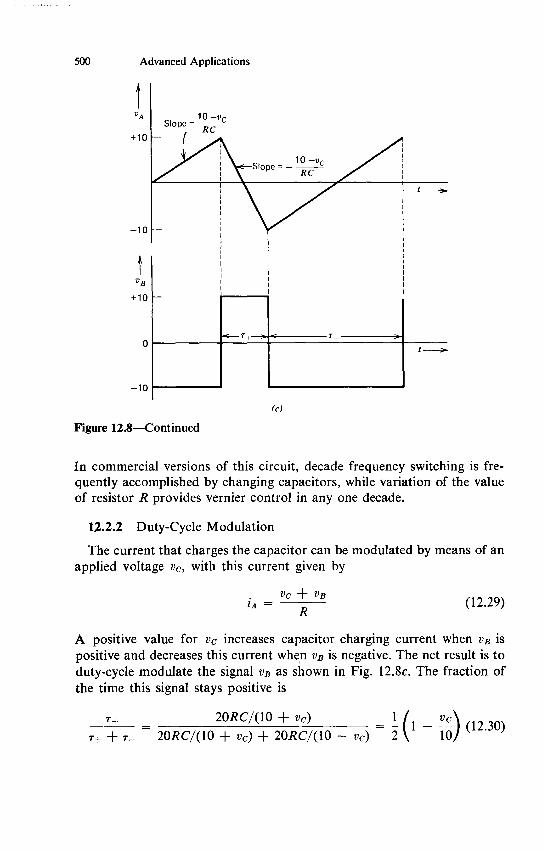
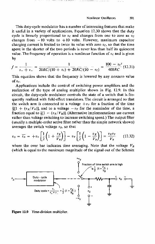

C
0 VB (a)
VA
+ VT
Slope= shy
t -
Slope= +C
-- VT shy
VB
VF
- VF 4VTRC
VF
(b)
Figure 1210 Voltage-controlled oscillator (a) Circuit (b) Waveforms
503
504 Advanced Applications
R R
+jVC I
-T
VA~I -0
R2
vK01
Limited to plusmn VM
(a)
t Vo
S+ VM
+V R1 R
1 +R 2
VA gt
Figure 1211 One amplifier nonlinear oscillator (a) Circuit (b) Inverting Schmittshytrigger characteristics (c) Waveforms
associated components that obeys the same differential equation as does the system under study The answers obtained consist of the responses of the electrical analog to particular inputs and initial conditions
Analog computers are available from several manufacturers These machines incorporate in addition to the necessary hardware a considerable human-engineering effort Summing amplifiers and integrators included in these machines are normally constructed with fixed scale factors so that external components need not be used For example several inputs with gains of - 1 and - 10 are typically provided for each summing amplifier
505
V
Analog Computation
Toward +VM with time constant RC+yMn
R +R2 V
tshy
-VM time constant R C
+VMv0
0- t -shy
(c)
Figure 1211-Continued
Potentiometers are also included and these devices are combined with
fixed-gain amplifiers to provide arbitrary gain levels Thus a gain of -312
might be realized by preceding a gain of - 10 amplifier with a potentiometer
set for an attenuation of 0312 Nonlinear elements such as function genshy
erators and multipliers are frequently included The inputs and outputs of
the various elements are usually connected to jacks of some type The intershy
connections necessary to simulate a particular system are then made with
patchcords that connect the various jacks In many cases the programming
(inserting the patchcords to establish the proper connection pattern) is
done on a board physically removed from the computer while other users
with their own boards solve their problems The board makes the required
connections when it is inserted into a mating plate located on the machine
While the accuracy of solutions obtained via analog computation is limited by component tolerances it normally far exceeds the accuracy required
for the simulation of physical systems which are themselves constructed
with imprecise components A further consideration is that it is frequently
506 Advanced Applications
possible to get a good physical feeling for a system via analog computation since many variables are available for observation and since the effects of parameter variations can be quickly investigated
Our treatment here can only cover the barest essentials and highlight a few of the ancillary circuits that were evolved for analog computation The reader interested in a detailed treatment of this fascinating and powerful technique is referred to Korn and Korn
1231 The Approach
Our objective here is to show how electronic-analog techniques are used to simulate differential equations that describe the systems to be studied We initially assume that the differential equation under investigation is linear and has the general form
d~x -x dx an dtx + a-1 dt-x + - + ai - + aox = f(t) (1234)dtn r- dt
It is certainly not necessary that the independent variable of the system under study be time as implied by Eqn 1234 For example if we were investigating the deflection of a bridge under static load we might be interested in vertical displacements from equilibrium as a function of disshytance from one end of the bridge However since our analog will use time as its independent variable we substitute time for the independent variable if necessary in the original equation Similarly we realize that any dependent variables in our analog will have to be voltages regardless of the variables they actually represent in the system under study
Equation 1234 is rewritten so that the highest derivative of x is expressed in terms of the other variables in the form
dx an_ 1 d- 1 x a1 dx aox 1 dtn andt~ dt-~ 1
- a~ d a~ + - f(t) (1235)dt--1 an dt an an
Equation 1235 can be represented as the block diagram shown in Fig 1212 In this representation the variable dnxdtn appears as the output of a summation point Inputs to the summation point are scaled multiples of the driving function and the lower-order derivatives of x The lower-order derivatives are obtained by successive integrations of dnxdtn with a total of n integrations required to complete the block diagram
Note that the only elements included in the block diagram are a multiple-input summation point inverters to precede some inputs on the summer
I G A Korn and T M Korn Electronic Analog and Hybrid Computers 2nd Edition McGraw-Hill New York 1972
f (t)
Figure 1212 Block diagram of Eqn 1235
(I
508 Advanced Applications
gain blocks and integrators Since each of these elements can be readily constructed using operational amplifiers and passive components the block diagram can be implemented using these devices When the analog realizashytion is excited with a voltage equal tof(t) voltages equal in value to x and its derivatives will be available as the outputs of the integrators
As an example of this process consider the differential equation
dex d3x d2x dx - + 261 d + 342 d2 + 261 + x = f(t) (1236)dt4 dt dts dt
(We recall from Section 332 that this equation represents a fourth-order Butterworth filter) Solving for d 4xdt yields
dex d3x d2x dx -= -261 - 342 - - 261 - x + f(t) (1237)
dt4 dt3 dt2 dt
One possible simulation of this equation is shown in Fig 1213 The voltages expected at the output of various amplifiers are indicated by writing the value of the variable the voltage represents at appropriate nodes Note that in contrast to traditional analog-computer methods gains are established by selecting impedances 4 used around operational amplifiers rather than by combining potentiometers with fixed-gain amplifiers and integrators Also functions have been combined in order to reduce the number of amplifiers required The use of inverting connections only is traditional in analog computation and reflects that fact that an operashytional-amplifier design technique frequently used to improve d-c performshyance results in an amplifier that can only be used in inverting connections (See Section 1233) It may of course be possible to use noninverting integrators or summing amplifiers (realized with resistive summing at the input to a noninverting-amplifier connection) if general-purpose operashytional amplifiers are used for this simulation
The four integrators appear along the top of the diagram Since it is assumed that there is no need to have a voltage representing d 4xdt4 availshyable the summing operation is included in the first integrator connection The output of this integrator is - (dlxdt) when the indicated current is equal to (10-6 A) d 4xdt4 Since inverting integrators are used the signs associated with successive derivatives alternate The scaling and inversions required by the coefficients of x and its second derivative are obtained with the bottom amplifier
4The relative impedance levels shown in Fig 1213 are high if general-purpose operashytional amplifiers such as the LM101A are used Since only ratios are important in estabshylishing the transfer function all impedance levels can be scaled to reduce errors that result from amplifier input currents
Current here equals 1pF
(10-6 A) 4xdt47 1 pF
1 pF 1 M F
1pF
1 M261
1 M92
1 M92
M32
1 ME2
Figure 1213
-x -342 d dt
2
Simulation of fourth-order Butterworth equation
510 Advanced Applications
The number of amplifiers required in Fig 1213 indicates the general rule If this topology is used simulating an nth-order linear differential equation requires n integrators and one amplifier that inverts appropriate signals as necessary to complete feedback paths
Analog-computing techniques can also be used to solve a variety of nonshylinear differential equations by including hardware that implements the nonlinearity in the simulation As an example consider Van der Pols differential equation
dsx dx + y(x 2 - 1) + x = 0 (1238)
dt2 dt
where y is a positive constant For small values of x the coefficient of the first derivative term is negashy
tive and increasing-amplitude oscillations result When the amplitude of the oscillation becomes large enough the coefficient of the first derivative will be positive over part of the cycle and a limit cycle can result Equation 1238 is rewritten in a form convenient for simulation as
d 2 x dx dx = - - x (1239)
dtz dt dt
2Multipliers are required to generate x and form the x 2(dxdt) product necessary for the simulation of Eqn 1239 Two techniques for analog multiplication were described in Sections 1155 and 1222 Practical multishypliers based on these methods are often designed to have an output voltage equal to the product of the two input voltages divided by 10 volts for comshypatibility with the dynamic range of most solid-state operational amplifiers Figure 1214 shows a possible simulation of Eqn 1239 assuming that multipliers with this scale factor are used
Van der Pols equation is an example of an undriven differential equashytion and excitation is by initial conditions only While initial conditions were not mentioned in our earlier discussion of the simulation of linear differential equations we recognize that we must specify n initial conditions in order to determine the complete (homogeneous plus driven) solution of an nth-order differential equation These initial conditions can be set simply by establishing the voltages on the integrating capacitors at time t = 0 since these voltages are proportional to the values of x and its first n - I derivatives A circuit for setting initial conditions is described in Section 1233
The value of x as a function of time for Van der Pols equation with y = 025 is shown in Fig 1215 The initial conditions used for parts a and b of this figure are x(0) = 05 (dxdt)(0) = 0 and x(0) = 3 (dxdt)(0) = 0 respectively We see that in both cases the amplitude of the limit cycle conshy
511 Analog Computation
1 MG
- x 2 dx if x2
1 Mn 10_0 dt 10 IE Multiplier - - -- Multiplier
_1 1 Mamp2
Figure 1214 Simulation of Van der Pols equation
verges to a peak-to-peak value of approximately 4 Part c of this figure is a plot of dxdt versus x(t) This representation in which time is a parameter
along the curve is called a phase-plane plot The responses for both values
of initial conditions are included The convergence to equal-amplitude
limit-cycles for both sets of initial conditions is evident in this figure
The formal procedure described here is certainly not the only one which
results in a correct analog representation of a problem While it does lead
to a compact realization other realizations may maintain better correshy
spondence with the physical system that is being modeled One popular
alternative technique involves simply drawing a block diagram for the
system under study and then implementing the block diagram on a blockshy
by-block basis without ever writing down the complete system differential
equation While this approach often requires more hardware to complete
the simulation it is convenient in that voltages proportional to the actual
variables of interest in the problem under study are avaliable Furthermore it is generally possible using this alternative to associate scale factors with
the parameters of physical elements in the simulated systems on a one-toshy
one basis
x(t) 2 shy
0 020 t 30 (seconds)
-2shy(a)
4shy
t x(t)
2 shy
0__ 010 20 t 30
- v Y v(seconds)
-2 -
(b)
-4 shy
Figure 1215 Solution to d2xdt
2 + 025(x 2 - 1)(dx dt) + x = 0 (a) With initial
conditions x(0) = 05 (dx dt)(0) = 0 (b) With initial conditions x(0) = 3 (dx dt)(0) = 0 (c) Parts a and b repeated in phase-plane form
512
513 Analog Computation
I dx dt
x=3 dX 0dt
-5 x(t)
Direction of increasingtime
-4 Lshy
(c)
Figure 1215-Continued
1232 Amplitude and Time Scaling
Practical considerations constrain the amplitude and frequency range of the signals that arise in analog computation We normally prefer maxishymum signal levels that are comfortably below amplifier saturation levels but well above noise and offset uncertainties Similarly very low-frequency signals are difficult to integrate accurately while the limited gain of an operational amplifier at high frequencies compromises accuracy in this frequency range Amplitude scaling and time scaling are used to standardize signals to convenient amplitude levels and spectral content
Amplitude scaling involves little more than some additional bookkeeping effort Since we are using voltages for all of the dependent variables in our simulation there must be a dimensioned scale factor that relates the mashychine variables to the problem variables when the problem variables are quantities other than voltages For example if x is a displacement in meters and some voltage in a simulation represents this variable on a 1 meter = 1 volt basis the machine variable should really be labeled (1 voltmeter)x rather than simply x as is frequently done We should realize that the number associated with the scale factor can readily be selected to be other than unity Thus we might use lOx as the label for some voltage or preferably (10 voltsmeter)x If this voltage were 7 volts the correshysponding displacement would be x = (7 volts) (1 meter 10 volts) = 07 meter The appropriate values for scale factors can only be determined with a knowledge of approximate problem-variable levels since the correspondshying machine variables should have peak values slightly below the saturation
514 Advanced Applications
level Once scale factors have been selected they are implemented by modishyfying the gains of amplifiers and integrators from their initially selected values
Time scaling has advantages beyond those of centering signal-frequency components within the range of optimum operational-amplifier performshyance Consider for example the simulation of a planetary motion problem that may require years of real time to complete Using a faster machine time scale permits us to obtain the solution in a more reasonable time interval Similarly the use of a slower than real time scaling procedure allows us to display the buildup of charge in the base region of a transistor at a rate comfortable for viewing on a display oscilloscope
The technique used for time scaling involves the substitution
t = or (1240)
where r is machine time and is equal to real time divided by a scale factor 0 A value of a-greater than one implies that the machine solution is faster than the actual solution so that one second of real time is represented by a shorter period r of machine time
This process is illustrated using the form for a differential equation given in Eqn 1234 and repeated here for convenience
dux ux dx an dt + an_1 dtx + + a dt + aox = f(t) (1234)
dtn dr-1dt
In order to apply the substitution of Eqn 1240 we change f(t) tof(-r) and change dmxdtm to (lum)(dxdrm) Thus the time-scaled version of Eqn 1234 is
an dax an_1 dux dxa1 - d+xplusmn d + -lx plusmn- + aox = f(r) (1241) e-ndr an- 1 dr- o dr
The equation when simulated will have a solution identical in form to that of Eqn 1234 but will run a factor of a-faster than the original equation
A second way to implement time scaling is to realize that the dynamics of the simulation are implemented by means of integrations and that changshying the scale factor of every integrator in the simulation by some factor must change the time scale of the simulation by precisely the same factor Thus problems can be time scaled by first simulating the problem for a
real-time solution and then dividing the value of every capacitor by a
factor of a Alternatively every resistor used to implement all integrators can be reduced in value by a factor of a or the scale-factor change can be apportioned between resistors and capacitors The net result of any of these modifications will be to make the problem on the machine run a factor ofa faster than the real-time solution It is of course still necessary to increase the speed of driving functions applied to the system by a factor of a if these
515 Analog Computation
signals are derived from sources that are not implemented using scaled integrators
The coefficients of the original differential equation often can be used to determine the time scale appropriate to a particular problem If the roots of the characteristic equation have approximately equal magnitudes the natural frequencies of the undriven solution will be the order of
w - (1242)(a Conversely if the system is dominated by one pole the characteristic freshyquency is the order of
ao (1243) ai
The characteristic frequencies given by Eqn 1242 or 1243 can be changed to values convenient for display and compatible with operational-amplifier performance by appropriate selection of a
The element values that occur in a problem simulation often provide clear indications of the need to modify amplitude or time scales If for example we find that high gain is required at the input of every amplifier being supplied with some particular signal the scale factor of that signal is probably too small relative to other amplitude scale factors used Simishylarly if one input resistor to a summing amplifier or an integrator is much larger than all other input resistors associated with the amplifier the implication is that the term applied to the input in question contributes little to the output of the summer or integrator In the case of time-scale selection an inappropriate choice is usually reflected by unreasonable resistor values capacitor values or both associated with integrators
The Van der Pol equation simulated earlier (Eqn 1238) is used as a simple example of time and amplitude scaling For the range of initial conditions used previously and with A = 025 the maximum magnitudes of x and dxdt are approximately 3 and 3 sec-1 respectively while the maximum magnitude of d 2xdt2 is slightly greater than 3 sec-2 Accordshy
ingly if 10-volt maximum amplifier outputs are assumed scale factors of 3 volts per unit for x and dxdt combined with a scale factor of 2 volts per unit for d 2xdt2 are reasonable If Eqn 1239 is rewritten using these scale factors we obtain
d2x 2 dx 2 dx 2
2 -= - y(3x)2 3 + - 3- - (3x) (1244)dt2 27 dt 3 dt 3
The simulation diagram again assuming that multipliers with outputs equal to the product of the inputs divided by 10 are used is shown in Fig 1216 It has also been assumed in forming this diagram that a voltage
516 Advanced Applications
proportional to d2xdt2 is required Note that the input signals applied to the first amplifier are negatives of the right-hand side of Eqn 1244 because of the inversion associated with this amplifier The transfer funcshytion of the first integrator is -(32s) so that it provides an output of -3(dxdt) when driven with 2(d 2xdt2) Alternate scaling may be advanshytageous if different values of y are used to keep the maximum magnitudes of the voltages proportional to dxdt and d 2xdt2 at optimum levels
If a value of RC = 1 second is used the solution will run at real time and the oscillation frequency will be about one radian per second Changing this product will time scale the solution For example the use of RC = 1 ms results in limit-cycle oscillation at approximately 1000 radians per second
1233 Ancillary Circuits
There are several interesting circuit configurations that are frequently employed in analog computation and that also can be used in other more general applications
One of these topologies is the three-mode integrator We have seen that it is necessary to apply initial conditions to integrators in order to obtain complete (homogeneous plus driven) solutions for simulated differential
1MG C
C
2 X dt2 -3 yx
dt
3 + R 3
Figure 1216 Scaled simulation of Van der Pols equation
517 Analog Computation
equations Another useful computing mode results if all integrators are simultaneously switched to a state where their outputs become time inshyvariant and thus hold the values that were present at the switching time The values of problem variables at the switching time can then be detershymined accurately with a digital voltmeter
The three-mode integrator shown in Fig 1217 permits application of initial conditions and allows holding an output voltage in addition to functioning as an integrator The reset (or initial condition) operate and hold modes are selected by appropriate choice of switch positions With switch D open and switch o closed the amplifier closed-loop transfer function is
V0(s) __ 1 V(S) RC(1245) V-(s) R2Cs + 1
If VA is time invariant in this mode the capacitor will charge so that the output voltage eventually becomes the negative of VA The capacitor voltage can then provide initial conditions for subsequent operations
If switch o is closed and switch o is open the amplifier integrates VB in the usual fashion
With both switches open capacitor current is limited to operational-amplifier input current and capacitor self-leakage thus capacitor voltage is ideally time invariant
C
R||
VB
R2 R2
VA
Figure 1217 Three-mode integrator
518 Advanced Applications
The required reset time of the connection shown in Fig 1217 can be quite long if reasonable values are used for the resistors labeled R2 The use of a second operational amplifier connected as a voltage follower and supplying a low-resistance drive for the inverting input of the integrator can substantially shorten reset times A practical three-mode integrator circuit that incorporates this feature is shown in Fig 1218
The bipolar-transistor drivers are compatible with T2L logic signals and drive the gate potential of field-effect-transistor switches to ground on inputs that exceed two diode forward voltages With a high level for the operate signal and the reset signal at ground Q1 is on and Q2 is off This combination puts the circuit in the normal integrating mode FET Qi has a drain-to-source on resistance of approximately 25 ohms and this value is compensated for by reducing the integrating-resistor size by a
+15V +15V +15V
10 kE2
Reseton high
-15 V
Input to be Q1 2N4391 integrated
Output
Initial-condition input
Figure 1218 Circuit for three-mode integrator
519 Analog Computation
corresponding amount Diode D1 does not conduct significant current in this state Diodes D2 and D3 keep the output of the follower within approxishymately 06 volt of ground One benefit of this clamping is that the source of Q2 cannot become negative enough to initiate conduction with its gate at - 15 volts since the maximum pinchoff voltage of the 2N4391 is 10 volts Clamping the follower input level also keeps its signal levels near those anticipated during reset thus avoiding long slewing periods when the circuit is switched to apply initial conditions
With the gate of Q1 at - 15 volts (corresponding to a low level on the operate control line) diode D1 prevents source potentials that would initiate conduction of transistor Q1 If Q2 is on the output voltage is driven toward the negative of the initial-condition input-signal level The details of the transient for a large error depend on diode FET and amplifier characteristics As the error signal becomes smaller the reset loop enters its linear operating region The reader should convince himself that the linear-region transmission of the reset loop (assuming ideal operational amplifiers) is - l2rdCs where rd is the incremental drain-to-source on resistance of the FET Thus the low FET resistance rather than R2 detershymines linear-region dynamics
The hold mode results with both the operate and the reset signals at ground so that both FETs are off In this state the current supplied to the capacitor is determined by FET leakage and amplifier input current
One application for this type of circuit in addition to its use in analog computation is as a sample-and-hold circuit In this case the operate switch is not needed and the circuit is switched from sampling the negative of an input voltage to hold with Q2
Sinusoidal signals are frequently used as test inputs in analog-computer simulations A quadrature oscillator that includes limiting and that is easily assembled using components available on most analog computers is shown in Fig 1219 The diagram implies a simulated differential equation prior to limiting of
- 2 C2 d RCdv + v0 (1246) dt2 K dt
We recognize this equation as a linear second-order differential equation with c = 1RC and = - 12K The value of K is chosen small enough
to guarantee oscillation with anticipated capacitor losses and amplifier imperfections thus insuring that signal amplitudes will be determined primarily by the diode-resistor networks shown
A precisely known voltage reference is required in many simulations to apply constant input signals provide initial-condition voltages function as a bias level for nonlinearities or for other purposes Voltage references are also used regularly in a host of applications unrelated to analog simulation
R2 R2
C R3 R3
R
RRCdt R
RIR
-RCC
dR
Figure 1219 Quadrature oscillator with limiting
521 Analog Computation
The circuit shown in Fig 1220 is a simple yet highly stable voltage refershyence The operational amplifier is connected for a noninverting gain of slightly more than 15 so that a 10-volt output results with 64 volts applied to the noninverting amplifier input
With the topology as shown the voltage across the resistor connected from the amplifier output to its noninverting input is constrained by the amplifier closed-loop gain to be 0562 Vz where Vz is the forward voltage of the Zener diode The current through this resister is the bias current apshyplied to the Zener diode Zener-diode current is thus established by the stable value of the Zener voltage itself The Zener output resistance does not deteriorate voltage regulation since the diode is operated at constant current in this connection The filter following the Zener diode helps to attentuate noise fluctuations in its output voltage
An emitter follower is included inside the operational-amplifier loop to increase output current capacity (current limiting circuitry as discussed in Section 84 is often a worthwhile precaution) and to lower output impedshyance particularly at higher frequencies While the low-frequency output impedance of the circuit would be small even without the follower because of feedback this impedance would increase to the amplifier open-loop output impedance at frequencies above crossover The emitter follower reduces open-loop output impedance to improve performance when pulsed or high-frequency load-current changes are anticipated A shunt capacitor at the output may also be used to lower high-frequency output impedance (See Section 522)
Start-up diode
V +5 V
64 V
Temperature shycompensated 0562 R1 Zener diode
Trim to -adjust output
voltage
Figure 1220 Voltage reference
522 Advanced Applications
The bootstrapping used to excite the Zener diode is of course a form of positive feedback and would deteriorate performance if the magnitude of this feedback approached unity The low-frequency transmission of the positive feedback loop is
L = 1562 rd - (1247)R + rd
where rd is the incremental resistance of the Zener diode This expression is evaluated using parameters for a 1N829A a temperature-compensated Zener diode The diode is designed for an operating current of 75 mA and thus R will be approximately 500 Q The incremental resistance of the diode is specified as a maximum of 10 Q Thus the loop transmission is from Eqn 1247 003 This small amount of positive feedback does not significantly affect performance
The positive feedback can result in the circuit operating with the diode in its forward-conducting state rather than its normal reverse-breakdown mode This state which leads to a negative output of approximately one volt can be eliminated with the start-up diode shown The start-up diode insures that the Zener diode is forced into its reverse region but does not contribute to Zener current under normal operating conditions
The expected operational-amplifier imperfections have relatively little effect on the overall performance of the reference circuit A value of 30000 for supply-voltage rejection ratio (typical for integrated-circuit amplifiers) causes a change in output voltage of approximately 50 AV per volt of supply change (This 33 yVV sensitivity is amplified by the closed-loop gain of 15) The typical input-voltage drift for many inexpensive operashytional amplifiers is the order of 5 MV per degree Centigrade This figure is not significant compared to the temperature coefficient of 5 parts per million per degree Centigrade or approximately 32 MV per degree Centishygrade of a high-quality Zener diode such as the 1N829A
The designers of the large analog computers that evolved during the period from the early 1950s to the mid-1960s often devoted almost fanatical effort to achieving high static accuracy in their computing elements Toward this end operational amplifiers were surrounded with high-precision wire-wound resistors and capacitors that could be accurately trimmed to desired values These passive components were often placed in temperature-stable ovens to eliminate variations with ambient temperature
The low-frequency errors (particularly input voltage offset) characteristic of vacuum-tube operational amplifiers were largely eliminated by means of an imaginative technique known as chopper stabilization5 This method
IE A Goldberg Stabilization of Wide-Band Direct Current Amplifiers for Zero and Gain RCA Review Vol II No 2 June 1950 pp 296-300
Figure 1221 Chopper-stabilized amplifier
LA
524 Advanced Applications
is still incorporated into some modern operational-amplifier designs and it provides a way of reducing the voltage drift and input current of an amplifier to vanishingly small levels The usual implementation of this technique can be viewed as an extreme example of feedforward (see Section 822) and thus results in an amplifier that can only be used in inverting connections
Figure 1221 illustrates the concept Assume that the optional network is eliminated so that the junction of Zf and Z is connected directly to the inverting input of the top amplifier The resulting connection clearly funcshytions as an inverting amplifier if the voltage vc is zero Observe that one necessary condition for the amplifier closed-loop gain to be equal to its ideal value is that VA = 0 The objective of chopper stabilization is to reduce VA to nearly zero by applying an appropriate signal to the non-inverting input of the top amplifier
The d-c component of the voltage VA is determined with a low-pass filter and this component (VB) is chopped (converted to a square wave with peak-to-peak amplitude VB) using a periodically operated switch (Early designs used vibrating-reed mechanical switches while more modern units often use periodically illuminated photoresistors or field-effect transistors as the switch) The chopped a-c signal can be amplified without offset by an a-c amplifier and demodulated to produce a signal yc proportional to VB If the gain of the a-c amplifier is high the low-frequency gain VCVA = a0 2
will be high If a02 is negative the signal applied to the positive gain input of the top amplifier will be of the correct polarity to drive VA toward zero Arbitrarily small d-c components of VA can theoretically be obtained by having a sufficiently high magnitude for a02 although in practice achievable offsets are limited by errors such as thermally induced voltages in the switch itself The low-pass filter is necessary to prevent sampling errors that arise if signals in excess of half the chopping frequency are applied to the chopper
An alternative way to view the operation of a chopper-stabilized amplifier is to notice that high-frequency signals pass directly through the top amplishyfier while components below the cutoff frequency of the low-pass filter are amplified by both the bottom amplifier and the top amplifier in cascade (It is interesting to observe that low-frequency open-loop gain magnitudes in excess of 10 have been achieved in this way) It is therefore not necessary to apply low-frequency signals directly to the top amplifier and a high-pass filter (shown as the optional network) can be included in series with the inverting input of the top amplifier As a result both voltage offset and input current to the operational amplifier can be reduced by chopper stabilization yielding an amplifier with virtually ideal low-frequency characteristics
Several manufacturers offer packages that combine discrete-component choppers with integrated-circuit amplifiers More recently integratedshy
525 Active Filters
C1 v
Figure 1222 Second-order low-pass active filter
circuit manufacturers have been able to fabricate complete chopper-stabilized amplifiers either in monolothic form or by combining several monolithic chips to form a hybrid circuit These circuits incorporate topological improvements that permit true differential operation The large capacitors required are connected externally to the package Drifts of a fraction of a microvolt per degree Centigrade coupled with input currents in the picoampere range are available at surprisingly low cost
124 ACTIVE FILTERS There are numerous applications that require the realization of a particushy
lar transfer function One of the many limitations of the design of filter networks using only passive components is that inductors are required to obtain complex pole locations This restriction is removed if active elements are included in the designs and the resultant activefilterspermit the realizashy
tion of complex poles using only resistors and capacitors in addition to the active elements Further advantages of active-filter synthesis include the possibility of a wide range of relative input and output impedances and the use of smaller less expensive reactive components than is normally possible with passive designs
There is a fair amount of present research devoted toward improving techniques for active-filter synthesis and the probability is that better deshysigns particularly with respect to sensitivity (the dependence of the transfer function on variations in parameter values) will evolve This section deshyscribes two presently popular topologies that can be used to realize active filters
1241 The Sallen and Key Circuit6
Figure 1222 shows an active-filter circuit that uses a unity-gain-conshynected operational amplifier Node equations for the circuit are easily
I R P Sallen and E L Key A Practical Method of Designing RC Active Filters Instishytute of Radio Engineers Transactions on Circuit Theory March 1955 pp 74-85
526 Advanced Applications
written by noting that the voltage at the noninverting input of the amplifier is equal to the output voltage and are
G1Vi =(G 1 + G2 + C2s)V - (G2 + C2 s)Vo (1248)
0 = -G 2 V + (G2 + C1s)V
Solving for the transfer function yields
V0(s) 1V(S shyCC2S2(1249)
Vi(s) R1 R 2C1 C2s2 + (R 1 + R2 )Cls + 1
This equation represents a second-order transfer function with standard-form parameters
n VR 1R2C1C2 (1250)
and
R1 + R 2 (1251)
2VR 1 R 2 C2
Since only two quantities are required to characterize the second-order filter the four degrees of freedom represented by the four passive-comshyponent values are redundant Part of this redundancy is frequently elimishynated by choosing R1 = R2 = R In this case the standard-form paramshyeters become
on (1252)R -C1C2
and
= (1253)
The addition of another section to the second-order low-pass active filter as shown in Fig 1223 allows the synthesis of a third-order transfer function with a single amplifier If equal-value resistors are used as shown the transfer function is
V 0(s) _ _____1________ V-(S - I 2S2(1254)
C1C2 2 (C1Vi(s) C3 Rs 3 + 2(C 1C3 + C2C3)R2s + + 3C3)Rs + 1
An nth-order low-pass filter is often designed by combining n2 second-order sections in the case of n even or one third-order section with n2 - 32 second-order sections when n is odd Tables7 that simplify
I Farouk Al-Nasser Tables Speed Design of Low-Pass Active Filters EDN March 15 1971 pp 23-32
527 Active Filters
C2
R R R
Figure 1223 Third-order low-pass active filter
element-value selection are available for filters up to the tenth order with a number of different pole patterns
Interchanging resistors and capacitors as shown in Fig 1224 changes the second-order low-pass filter to a high-pass filter The transfer function for this configuration is
2Vo(s) _ R1 R 2C1C 2s
Vi(s) R1R2C1C2s2 + R2(C1 + C2)s + 1
If in a development analogous to that used for the low-pass filter we choose C1 = C2 = C Eqn 1255 reduces to
V 0(s) s2_____________2 _
V-(S S2 W2(1256) V1(s) (s2 2) + (2 so) + 1
where
I
CVR1 R 2 and
R2
R 1
R2
Cy C2
7 ++
+iR -V 0~-1
Figure 1224 Second-order high-pass active filter
528 Advanced Applications
The Sallen and Key circuit can be designed with an amplifier gain other than unity (see Problem P128) This modification allows greater flexibility since the low- or high-frequency gain of the circuit can be made other than one However the damping ratio of transfer functions realized in this way is dependent on the values of resistors that set the closed-loop amplifier gain thus poles may be somewhat less reliably located A further advantage of the unity-gain version is that it may be constructed using the LM 110 inteshygrated circuit (see Section 1044) The bandwidth of this amplifier far exceeds that of most general-purpose integrated-circuit units and corner frequencies in the low megahertz range can be obtained using it
1242 A General Synthesis Procedure
The Sallen and Key configuration together with many other active-filter topologies allows-complete freedom in the choice of pole location but does not permit arbitrary placement of transfer-function zeros The application of the analog-computation concepts described in Section 1231 allows the synthesis of any realizable transfer function that is expressable as a ratio of polynomials in s provided that the number of poles is equal to or greater than the number of zeros in the transfer function
Consider the transfer function
V(s) _ b s + bn_1 s-1 + - + b1s + bo (1257) Vi(s) as + ans 1 + - + ais + ao
The first step is to introduce an intermediate variable V(s) such that Vj(s) Vi(s) contains only the poles of the transfer function or
Va(S) 1(1258)Vi(s) ans + a_s--1 + + ais + ao
Proceeding in a way exactly parallel to the time-domain development of Section 1231 we write
SVa(S-(s) - -a s V(s) - ao Va(S) + Vi(s) (1259) a an an a
The block-diagram representation of Eqn 1259 is shown in Fig 1225 This block diagram can be readily implemented using summers and inteshygrators In order to complete the synthesis of our transfer function (Eqn 1257) we recognize that
V(s) = Va(s) (b s + bs-- + - + bis + bo) (1260)
The essential feature of Eqn 1260 is that it indicates V(s) is a linear comshybination of Va(s) and its first n derivatives Since all of the necessary varishy
Figure 1225 Block diagram representation of transfer function that contains only poles
LAi
530 Advanced Applications
ables appear in the block diagram V(s) can be generated by simply scaling and summing these variables without the need for differentiation
This synthesis procedure is illustrated for an approximation to a pure time delay known as the Pad6 approximate The time delay has a transfer function e-1 where r is the length of the delay The magnitude of this transshyfer function is one at all frequencies while its negative phase shift is linearly proportional to frequency The time delay has an essential singularity at the origin and thus cannot be exactly represented as a ratio of polynomials in s
The Taylors series expansion of e- 7 is
s22 SmnTm e- = 1 - sr + - + - - - + (-1) + - (1261)
2 M
The Pade approximates locate an equal number of poles and zeros so as to agree with the maximum possible number of terms of the Taylors series expansion This approximation always leads to an all-pass network that has right-half-plane zeros and left-half-plane poles located symmetrically with respect to the imaginary axis This type of singularity pattern results in a frequency-independent magnitude for the transfer function
Since we can always frequency or time scale at a later point we consider a unit time delay e- to simplify the development The first-order Padd approximate to this function is
I - (s2) s2 s 3
= 1-splusmn - +-- + - + (1262)1 + (s2) 2 4
The expansion for e- is
2 5 s s3 s4 s s6
e-= 1- s +-- + + - + (1263)2 6 24 120 720
The first-order approximation matches the first two coefficients of s of the complete expansion and is in reasonable agreement with the third coefficient This match is all that can be expected since only two degrees of freedom (the location of the pole and the location of the zero) are available for the first-order approximation The second-order Pad6 approximate to a one-second time delay is
1 - (s2) + (s212)
1 + (s2) + (S212)
s4S2 s 3 s5
-s+ + - - - - ---+ (1264)2 6 24 144
531 Active Filters
x0
s plane
X 0
Figure 1226 Singularity locations for second-order Pade approximate to one-
second time delay
As expected the first four time-delay coefficients of s are matched by the
approximation The s-plane plot for P 2(s) is shown in Fig 1226 Simple
vector manipulations confirm the fact that the magnitude of this function
is one at all frequencies The phase shift of the approximating function is (from Eqn 1264)
4 P2(jo) = 2 4 1 - + (I] 2 tan- 1 2 [1 - C212)] (1265)
This function is compared with an angle of - 573cr (the value for a one-
second time delay) in Fig 1227 We note excellent agreement to frequencies
of approximately 2 radians per second implying that the approximation
represents the actual function well for sinusoidal excitation to this freshy
quency with increasing discrepancy at higher frequencies The error reshy
flects the fact that the maximum negative phase shift of the Pad6 approxishy
mate is 360 while the time delay provides unlimited negative phase shift
at sufficiently high frequency
Synthesis is initiated by defining an intermediate variable Va(s) in accordshy
ance with Eqns 1258 and 1259 or
V-(s) -1 (1266)V(s) (s212) + (s2) + 1
and
S2 Va(S) = -- 6sVa(s) - 12 V(s) + 12Vi(s) (1267)
532 Advanced Applications
o (radsec) -3
4 5 6 7 8 90 1 2 3
-900
Phase shift of second-order Pade approximate to one-second
-180- time delay
t Phase shift of
-270 - one-second time delay
-360 shy
-450shy
-540shy
Figure 1227 Comparison of time delay and Pad6 approximate phase characteristics
The output voltage is
S2 s V0(s) - V(S) - - Va(S) + Va(S) (1268)
12 2
The operational-amplifier synthesis shown in Fig 1228 provides the required transfer function if RC = 1 second The reader should convince himself that the liberties taken with inversions and various resistor values do in fact lead to the desired relationship
Anticipated amplitudes depend on the input-signal level and its spectral content For example if a step is applied to the input of the circuit the magnitude of the signal out of the first amplifier must initially be 12 times as large as the step amplitude since the outputs of the integrators cannot change instantaneously to subtract from the input-signal level Note howshyever that the input-to-output transfer function of the circuit remains the same for any values of R1 = R2 If for example 10-V step changes are expected at the input selection of R1 = R2 = 120 kQ will limit the signal level at the output of the first amplifier to 10 volts while maintaining the correct input-to-output gain
The circuit shown in Fig 1228 was constructed using R = 100 kQ and C = 001 MF values resulting in an approximation to a 1-ms time delay This choice of time scale is convenient for oscilloscope presentation The
R2= 10 kE2
Vt -V
Y Y Y
A Figure 1228 Synthesis of second-order Pade approximate to a time delay
200 mV
I T
(a) 1 ms
200 mV
(b) 1 Ms
Figure 1229 Input and output signals for second-order Padd approximate to a 1-ms time delay (a) Sine-wave excitation (b) Triangular-wave excitation (c) Square-wave excitation
534
535 Active Filters
200 mV
I T
(c) 1 ms
Figure 1229-Continued
input and output signals for 100-Hz sine-wave excitation are shown in Fig 1229a The time delay between these two signals is 1 ms to within instrushymentation tolerances This performance reflects the prediction of Fig 1227 since good agreement to 2000 radsec or 300 Hz is anticipated for the apshyproximation to a 1-ms delay
Input and output signals for 100-Hz triangular-wave excitation are comshypared in Fig 1229b The triangular wave contains only odd harmonics and these harmonics fall off as the square of their frequency Thus the amplitude of the third harmonic of the triangular wave is approximately 11 of the amplitude of the fundamental the amplitude of the fifth harmonic is 4 of the fundamental while higher harmonics are further attentuated We notice that the circuit does very well in approximating a 1-ms time delay most of the time The aberration that results immediately following a change in slope reflects the inability of the circuit to provide proper phase shift to the higher-frequency components
The performance of the circuit when excited with an 100-Hz square wave is shown in Fig 1229c The relatively poorer behavior in the vicinity of a transition in this case results from the higher harmonic content of the square wave (Recall that the square wave contains odd harmonics that fall off only as the first power of the frequency)
536 Advanced Applications
125 FURTHER EXAMPLES
It was mentioned in the introduction to Chapter 11 that the objective of
the application portion of this book was to illustrate concepts for design
rather than to provide specific detailed examples in the usually futile
hope that the reader could apply them directly to his own problems
Successful design almost always involves combining bits and pieces a
concept here a topology there to ultimately arrive at the optimum solution
In this section we will see how some of the ideas introduced earlier are
combined into relatively more sophisticated configurations The three
examples that are presented are all real world in that they reflect actual
requirements that the author has encountered recently in his own work
1251 A Frequency-Independent Phase Shifter
There are a number of operational-amplifier connections such as the
approximation to a time delay described in the previous section that have
a transfer-function magnitude independent of frequency combined with
specified phase characteristics The phase shifter shown in Fig 1230 is
another example of this type of circuit We recognize this circuit as a differshy
ential-amplifier connection and thus realize that its transfer function is
V__s = 2RCsRs-1V0(s) = _2RC - 1 = RCs -1 (1269) Vi(s) RCs + 1 RCs + 1
This transfer function (which is the negative of a first-order Pade approxishy
mate to a time delay of 2RC seconds) produces a phase shift that varies from
- 1800 at low frequencies to 0 at high frequencies If a potentiometer or a
field-effect transistor is used for R the phase shift can be manually or
electronically varied
R1
R1
+ c RVi n
Figure 1230 Adjustable phase shifter
537 Further Examples
Input sinusoid Output sinusoid
shifter
Integrator
multiplier
Figure 1231 Constant phase shifter using a phase detector
One technique for converting resolver8 signals to digital form requires that a fixed 900 phase shift be applied to a sinusoidal signal with no change in its amplitude The frequency of the signal to be phase shifted may change by a few percent Unfortunately there are no finite-polynomial linear transfer functions that combine frequency-independent magnitude characshyteristics with a constant 900 phase shift While approximating functions do exist over restricted frequency ranges the arc-minute phase-shift constancy required in this application precluded the use of such functions We note that since a very specific class of input signals (single-frequency sinusoids) is to be applied to the phase shifter linearity may not be a necessary conshystraint Nonlinear circuits in spite of our inability to analyze them systeshymatically often have very interesting properties
Consider the configuration shown diagrammatically in Fig 1231 as a possible solution to our problem In this circuit an all-pass phase shifter with a voltage-variable amount of phase shift is the central element The circuit shown in Fig 1230 with a field-effect transistor used for the resistor R can perform this function The multiplier is used as a phase detector If the magnitude of the phase shift between the input and output signals is less than 900 the average value of the multiplier output will be positive while if this magnitude is between 90 and 1800 the average multiplier outshyput signal will be negative The integrator which provides the control
8 A resolver is basically a transformer with a primary-to-secondary coupling that can be varied by mechanically changing the relative alignment of these windings This device is used as a rugged and highly accurate mechanical-angle transducer
538 Advanced Applications
voltage for the FET in the phase shifter filters the second harmonic that results from the multiplication and supplies the loop gain necessary to keep the average value of the multiplier output at zero thus forcing a 900 phase shift between input and output signals Although the circuit described above can result in moderate accuracy a detailed investigation indicated that meeting the required specifications probably was not practical with this topology
It is worth noting that while the basic approach described above was not used in this case it is a valuable technique that has a number of interesting and useful variations For example the phase shift of a second-order high-or low-pass active filter is plusmn90 when excited at its corner frequency Tracking filters can be realized by replacing the fixed resistors in an active filter with voltage-controlled resistors and using a phase comparison to locate the corner frequency of the filter at its excitation frequency
In some applications other types of phase detectors are used One possishybility involves high-gain limiters that produce square waves with zero crossshying synchronized to those of the sine waves of interest The duty cycle of an exclusive OR gate operating on the square waves indicates the relative phase of the original signals
The previous circuit combined an all-pass network that provides a transfer-function magnitude that is independent of frequency with feedback which forces 90 of phase shift at the operating frequency An alternative approach is to combine a network that provides 90 of phase shift at all frequencies (an integrator) with feedback that forces its gain magnitude to be one at the operating frequency
The circuit that evolved to implement the above concept is shown in only slightly simplified form in Fig 1232 The signal integrator provides the required 90 of phase shift Its scale factor is adjusted by means of the field-effect transistor so that a gain magnitude of one is provided at frequencies close to the nominal operating value of 400 Hz Half of the drain-to-source voltage of the field-effect transistor is applied to its gate to linearize the drain-to-source resistance as described in Section 1214 The unity-gain buffer amplifier prevents current flowing through the FET-gate network from being integrated The capacitor in series with the signal-integrator input reshysistor and the resistor shunting the integrating capacitor are required to keep this integrator from saturating as a consequence of input voltage offset and bias current While they change the ideal phase shift by a total of approxishymately eight arc minutes this value is trimmed out along with other phase-shift errors with a network (not shown) following the integrator
The two full-wave precision-rectifier connections combine with the loop-gain integrator to provide an average current into the capacitor of this
0039 yF
Input (400 Hz)
375 kS2
U
Figure 1232 Precision phase shifter with amplitude control
540 Advanced Applications
integrator that is proportional to the difference between the magnitudes of
the input and output signals If for example the output-signal magnitude
exceeds the input-signal magnitude the voltage out of the loop-gain inteshy
grator is driven negative This action increases the incremental resistance
of the FET thus decreasing the signal-integrator scale factor and lowering
the magnitude of the output signal The inputs to the precision rectifiers are
a-c coupled so that d-c components of these signals do not influence the
rectifier output signals A two-pole low-pass filter follows the loop-gain
integrator to further filter harmonics that would degrade signal-integrator
performance The maximum positive output level of the loop-gain integrator is clamped
via an internal node to a maximum output level of zero volts in order to
eliminate a latch-up mode If this voltage became positive the FET would
conduct gate current and this current could cause the signal-integrator
output to saturate As a result the a-c component of the signal-integrator
output would be eliminated and the loop in an attempt to restore equishy
librium would drive the output of the loop-gain integrator further positive
The diode clamp prevents initiation of this unfortunate chain of events
The circuit shown in Fig 1232 has been built and tested at operating
frequencies between 395 and 405 Hz over the temperature range of 00 to
50 Centigrade (The feedback also eliminates the effects of signal-integrator
component-value changes with temperature) The input- and output-signal amplitudes remain equal within I mV peak-to-peak at any input-signal
level up to 20 volts peak-to-peak The phase shift of the circuit with a 20shy
volt peak-to-peak input remains constant within one arc minute While the
actual phase shift is not precisely 90 the constant component of the phase
error can be trimmed out as described earlier
1252 A Sine-Wave Shaper
We have discussed certain aspects of a function-generator circuit that
combines an integrator and a Schmitt trigger to produce square and triangle
waves in Sections 633 and 1221 Commercial versions of this circuit
usually also provide a sine-wave output that is synthesized by the seemingly
improbable method of shaping the triangle wave with a piecewise-linear
network This technique is practical because of the ease of generating
variable-frequency triangular waves and because the use of relatively few
segments in the shaping network gives surprisingly good sine-wave fidelity
Part of the design problem is to determine how the characteristics of the
shaping network should be chosen to best approximate a sine wave The
parameters that define the network are shown in Fig 1233 A total of n
break points are located over the input-variable range of 00 to 90 The
541 Further Examples
Slope = KS
-90 -on 61 62 on 900 0
SI
Slope = KS
Figure 1233 Piecewise-linear network characteristics
slope of the input-output transfer relationship is KSm between 0 = 0m and
o = 6m+1 The multiplying constant K reflects the fact that only relative slopes are important since a multiplicative change in all slopes changes only the magnitude of the input-output transfer characteristics The symshy
metry of the transfer characteristics about the origin insures that the output signal will have no d-c component and will contain no even harmonics when a zero-average-value triangular signal is used as the input
The network specification involves the choice of n values of 0 (the breakshypoint locations) and n + 1 relative slopes It can be shown that if the Os
are selected such that
m 1800 Om = M 80 0 lt M lt n7 (1270)
2n + 1 shy
and slopes selected as
Sm = sin 0m+1 - sin Om 0 lt m lt n (1271a)
Sm= 0 m = n (1271b)
the first n odd harmonics will be eliminated from the output signal
The decision to use four break points in the realization of the sine shaper was based on two considerations With this number of break points outshy
542 Advanced Applications
put distortion resulting from imprecise break-point locations and slope values is comparable to the distortion associated with the piecewise-linear approximation unless expensive components are used to establish these parameters Furthermore an inexpensive integrated-circuit five-diode array is available This matched-diode array can be used for the four break points with the fifth diode providing temperature compensation as described in material to follow Equations 1270 and 1271 evaluated for n - 4 suggest break points located at input-variable values of 20 400 60 and 800 with relative segment slopes (normalized to a minimum nonzero slope of one) of 2879 2532 1879 1 and 0 respectively
With the transfer characteristics of the shaping network determined it is necessary to design the circuit that synthesizes the required function The discussion of Section 1153 mentioned the use of superdiode connections to improve the sharpness of break points compared to that which can be achieved with diodes alone This technique was not used for the sine shaper since the rounding associated with the normal diode forward characteristics actually improves the quality of the fit to the sine curve
The compressive type nonlinearities described in Section 1153 were realized using diodes to increase the feedback around an operational amplifier thus reducing its incremental closed-loop gain when a breakshypoint level was exceeded An alternative is to use diodes to decrease the drive signal applied to the amplifier to lower incremental gain This apshyproach simplifies temperature compensation The topology used is shown in Fig 1234
The input-signal level of 20 volts peak-to-peak corresponds to the input variable range of z90 shown in Fig 1233 Thus the break-point locashytions of L20 plusmn40 -60 and L800 correspond to input-voltage levels of plusmn222 volts plusmn444 volts plusmn667 volts and plusmn-+89 volts respectively Resistor values are determined as follows It is initially assumed that the diodes are ideal in that they have a threshold voltage of zero volts zero resistance in the forward direction and zero conductance in the reverse direction Assume that the R1-R2 path is to provide the break points at input voltages of plusmn 889 volts Since the inverting input of the operational amplifier is at ground potential the resistor ratio necessary to make the voltage at the midpoint of these two resistors plusmn 15 volts with plusmn 889 volts at the input is
R215 R2 1 5 = 01687 (1272)
R1 + R2 889
The ratios of resistor pairs R3-R 4 R5-R6 and RrRs are chosen in a similar way to locate the remaining break points
+10 V--shy
OA
-10 V------shy
Signal v
v +
+1
+ O -
Figure 1234 Simplified sine-wave shaper
544 Advanced Applications
The relative conductances of the resistive paths between the triangular-wave signal source and the inverting input of the operational amplifier are constrained by the relative slopes of the desired transfer characteristics as follows The closed-loop incremental gain of the connection is proportional to the incremental transfer conductance from the signal source to the current iA defined in Fig 1234 With the ratio of the two resistors in each path chosen in accordance with relationships like Eqn 1272 the increshymental transfer conductance is zero (for ideal diodes) when the input-signal magnitude exceeds 889 volts increases to 1(R1 + R 2) for input-signal magnitudes between 667 and 889 volts increases further to [1(R 1 + R 2)] + [1(R 3 + R 4)] for input-signal magnitudes between 444 and 667 volts etc If we define 1(R1 + R2 ) = G realizing the correct relative slope for input-signal magnitudes between 444 and 667 volts reshyquires
1 1 2 = 1S79G (1273)R +R 2 R 3 -+FR 4
The satisfaction of Eqn 1273 makes the slope in this input signal range 1879 times as large as the slope for input signals between 667 and 889 volts Corresponding relationships couple other resistor-pair values to the R1 -R 2 pair
The sets of equations that parallel Eqns 1272 and 1273 together with the selection of any one resistor value determine reistors R1 through R 8 The general resistance level set by choosing the one free resistor value is selected based on loading considerations and to insure that stray capacitance does not deteriorate dynamic performance
The circuit used for the sine shaper (Fig 1235) uses the standard 17oshytolerance resistor values that best approximate calculated values The five diodes labeled A and those labeled B are from two CA3039 integrated-circuit diode arrays One member of each array modifies the bias voltages to account for the diode threshold voltages and to provide temperature compensation The compensating diodes are operated at a current level of approximately half the maximum operating current level of the shaping diodes While this type of compensation clearly has no effect on the conshyductance characteristics of the shaping diodes the exponential diode characshyteristics actually improve the performance of the circuit as described earlier
Since this circuit is intended to operate to 1 MHz (a high-speed integrated-circuit operational amplifier with a discrete-component buffer to increase output-current capacity is used) capacitors are necessary at the output of the reference-voltage amplifiers to lower their output impedance at the switching frequency of the diodes The 15-V levels are derived from the
Triangle-wave D - t 78 2k input ~ - -r4I (20-volt peak-peak) OtuOtu
Figure 1235 Sine-wave shaper
546 Advanced Applications
200 Ts
Figure 1236 Output from sine-wave shaper
voltages that establish triangle-wave amplitude so that any changes in this
amplitude cause corresponding break-point location changes
The circuit produces approximate sine waves with the amplitude of any individual harmonic in the output signal at least 40 dB (a voltage ratio of 1001) below the fundamental This performance is obtained with no trimming If adjustments are made to null the offset of the operational
amplifier and empirical adjustments (guided by a spectrum analyzer) are
used to counteract component-value errors and to compensate for finite diode forward resistance the amplitude of individual output-signal harmonics can be reduced to 55 dB below the fundamental at low frequenshycies Performance deteriorates somewhat at frequencies above approxishy
mately 10 kHz because of reduced signal-amplifier open-loop gain
A 1-kHz output signal from the circuit is shown in Fig 1236
1253 A Nonlinear Three-Port Network
The realization of a device analog that may be of value in teaching the dynamic behavior of bipolar transistors requires a three-port network
547 Further Examples
VB E
VE - N
Figure 1237 Three-port network
defined by Fig 1237 The synthesis of this network is initiated by first
designing a circuit that provides the relationship
VN = VB - V0 exp [(VB- VE) (1274)
The parameter Vo as we might expect is related to the quantity Is for the
transistor being simulated and consequently a corresponding temperature
dependence is desirable There are a number of ways to simulate Eqn 1274 One topology that
is adaptable to further requirements is shown in Fig 1238 Since an evenshy
tual constraint is that the current at the VB input be zero a buffer amplifier
is used at this terminal The second amplifier is differentially connected
with an output voltage
VA = 2VE - VB (1275)
The third amplifier is also connected as a differential amplifier so that
VN = VE - (iT + iA)R (1276)
Since feedback keeps the inverting input terminal of the third amplifier at
potential VE
A A - VE VE -B (177)R R
00
+ vc
IT R
VB
+ VB
+N
VA
-I
VE
Figure 1238 Synthesis of exponential relationship
549 FurtherExamples
If we assume the usual transistor characteristics
ir Is jexp [(VB- 1i (1278)
Substituting Eqns 1277 and 1278 into Eqn 1276 yields the form reshyquired by Eqn 1275
VN = VB - RIs exp VE)] -(VB- (1279)
In order to complete the synthesis it is necessary to sample the current flowing at terminal N and make the current flowing at terminal E the negashytive of this current A modification of the Howland current source (see Section 1143) can be used The basic circuit with differential inputs is shown in Fig 1239a (The reason for the seemingly strange input-voltage connection and the split resistor will become apparent momentarily) The current io for these parameter values is
22 (VA - vc) (VA - VA - vr) -2vr
o - (1280)R R R
In Fig 1239b the voltage source vr and half of the split resistor are reshyplaced with a Norton-equivalent circuit For equivalence it is necessary to make ir = 2vrR Expressing Eqn 1280 in terms of ir shows
io = -i (1281)
The topology of Fig 1239b shows that the iT current source can be reshyturned to ground rather than to voltage source VA This modification is shown in Fig 1239c the current-controlled current source necessary in our present application Note that the output is independent of VA the common-mode input voltage applied to the current source
The circuits of Figs 1238 and 1239c are combined to form the three-port network as shown in Fig 1240 In this circuit the feedback for the voltage vN is taken from the output side of the current-sampling resistor so that voltage drops in this resistor do not influence vN It is necessary to buffer the 100-kQ feedback resistor with a unity-gain follower to insure that current through this resistor does not flow through the current-sampling resistor and thus alter iE
The trim potentiometer allows precise matching of resistor ratios to make current iE independent of common-mode voltage levels at various points in the current source and thus dependent only on iN In this applicashytion it was not necessary to have exactly unity gain between iN and - iE so no trim is included for this ratio The general magnitude of the resistors
2R
R
VI
VA
(a)
2R
R
VA 1
i~ (b)
R 2R 1
R R 2 2 +
VA i A
R R
- R Load
o -
(c) Figure 1239 Current-controlled current source (a) Basic Howland current source (b) Current source following Norton substitution (c) Final configuration
550
I
Problems 551
VB
+ L- I----oVE 0-1249 k 2 249 k2 499 k E2 7j
100 k2
Figure 1240 Complete nonlinear three-port network
in the current source is chosen for compatibility with required current levels and amplifier characteristics and is not important for purposes of this discussion
PROBLEMS
P121 Consider a Wien-Bridge oscillator as shown in Fig 121 Show that if
the output signal is of the general form vo = E sin [(tRC) + 0] where 0 is a constant the signals applied to the two inputs of the operational amplishyfier are virtually identical a necessary condition for satisfactory performshyance Note that if the inverting and noninverting inputs are interchanged and it is assumed that the output has the form indicated above the signals at the two inputs will also be identical However this modified topology will not function as an oscillator Explain
P122 A Wien-Bridge oscillator is constructed using the basic topology shown
in Fig 121 Because of component tolerances the time constants of the series and parallel arms of the frequency-dependent feedback network
552 Advanced Applications
differ by 5 How must component values in the frequency-independent feedback path be related to guarantee oscillation
P123 Use a describing-function approach to analyze the circuit shown in Fig
123 assuming that the operational amplifier is ideal and that the diodes have zero conductance until a forward voltage of 06 volt is reached and zero resistance in the forward-conducting state In particular determine the magnitude of the signal applied to the noninverting input of the amplifier and the third-harmonic distortion present at the amplifier output
P124 A sinusoidal oscillator is constructed by connecting the output of a
double integrator (see Fig 1112) to its input Show that amplitude can be controlled by varying the magnitude of the (R2)-valued resistor shown in this figure Design a complete circuit that can produce a 20-V peak-to-peak output signal at 1 kHz Use a FET with parameters given in Section 1214 for the control element Analyze your amplitude-control loop to show that it has acceptable stability and a crossover frequency compatible with the 1-kHz frequency of oscillation If you have confidence in your design build it The 2N4416 field-effect transistor is reasonably well characterized by the parameters referred to above
P125 The discussions of Sections 1222 and 1223 suggest operating electronic
switches connected to symmetrical variable voltages from the output of a
t +v F
VIshy
_VF
Figure 1241 Infinite-gain limiter
Problems 553
Schmitt trigger for two different applications An alternative to the use of
switches is to use a circuit that has the transfer characteristic shown in
Fig 1241 for the necessary shaping function (In this diagram the voltage
VF is a positive variable) Design a circuit that uses operational amplifiers
to synthesize this transfer characteristic Your output levels should be
insensitive to temperature variations
P126
A magnetic-suspension system was described in Section 623 Develop
an electronic analog simulation of this system that permits determination
of the transients that result from disturbing forces applied to the ball
Assume that in addition to operational amplifiers and appropriate passive
components multipliers with a scale factor vo = vxvy 10 volts are available
A way to perform the division required in this simulation using a multishy
plier and an operational amplifier is outlined in Section 622 You may leave the various element values in the simulation defined in
terms of system parameters without developing final amplitude-scaled values
P127
A circuit intended for use as a precision voltage reference for an analog-
to-digital converter is shown in Fig 1242 The circuit uses a fraction of the
Zener-diode voltage as its output While this method involving resistive
attenuation results in relatively high output resistance compared with using
the voltage at the output of the amplifier as the reference the output
voltage becomes essentially independent of operational-amplifier offset voltage
R1
1N4779A- +
9 k2
Figure 1242 Voltage reference
554 Advanced Applications
C1
R R
Vi +
C2 R +I Ri
Figure 1243 Low-pass Sallen and Key circuit with voltage gain
The specified breakdown voltage of the 1N4779A is 85 volts 5 The indicated resistor is selected during testing to obtain the required output voltage independent of the actual value of the Zener-diode voltage
The breakdowh voltage range and the temperature coefficient of the device are guaranteed at an operating current of 0500 mA By proper choice of R1 and R 2 it is possible to make the current through the Zener diode independent of the actual Zener voltage after the single indicated selection has been completed Such a choice is advantageous since it simshyplifies circuit calibration as opposed to methods that require two or more
interdependent adjustments to set output voltage and Zener-diode operatshying current Find values for R1 and R 2 that result in this simplification (Please excuse the somewhat unwieldy numbers involved in this problem but it is drawn directly from an existing application)
P128 A Sallen and Key low-pass circuit with an amplifier closed-loop voltage
gain greater than unity is shown in Fig 1243 Determine the transfer function V 0(s)Vi(s) for this circuit Compare the sensitivity of this circuit to component variations with that of the unity-gain version
P129
One way to analyze the Sallen and Key circuit shown in Fig 1243 is to
recognize the configuration as a positive-feedback circuit If the loop is
broken at the noninverting input to the operational amplifier analysis
techniques based on loop-transmission properties can be used
(a) Indicate the loop-transmission singularity pattern that results when the
loop is broken at the point mentioned above It is not necessary to determine singularity locations exactly in terms of element values
Problems 555
(b) Show how the closed-loop poles of the system move as a function of the closed-loop gain of the operational amplifier by using root-locus methods that have been appropriately modified for positive feedback systems
P1210 Design a sixth-order Butterworth filter with a 1 kHz corner frequency
by cascading three unity-gain Sallen and Key circuits
P1211 The fifth-order Pad6 approximate to a one-second time delay is
1 - 05s + 0111s 2 - 139 X 10-2 s3
+ 992 X 10- 4s4 - 331 X 10- 5s5
1 + 05s + 0111s2 - 139 X 10- 2s3
+ 992 X 10- 4s4 + 331 X 10- 5s
Design an active filter that synthesizes this transfer function
P1212 Develop a linearized block-diagram for the system shown in Fig 1232
assuming that the FET is characterized by the parameters given in Section 1214 Show that the loop crossover frequency is low compared to 400 Hz for any input-voltage level up to 20 volts peak-to-peak Estimate the time required for the system to restore equilibrium following an incremental perturbation (initiated for example by a change in input frequency) when the input-signal amplitude is 100 mV peak-to-peak Note that the system is not significantly disturbed by a change in input amplitude when operating under equilibrium conditions and that therefore this relatively long settling time does not deteriorate performance
MIT OpenCourseWarehttpocwmitedu
RES6-010 Electronic Feedback SystemsSpring 2013
For information about citing these materials or our Terms of Use visit httpocwmiteduterms
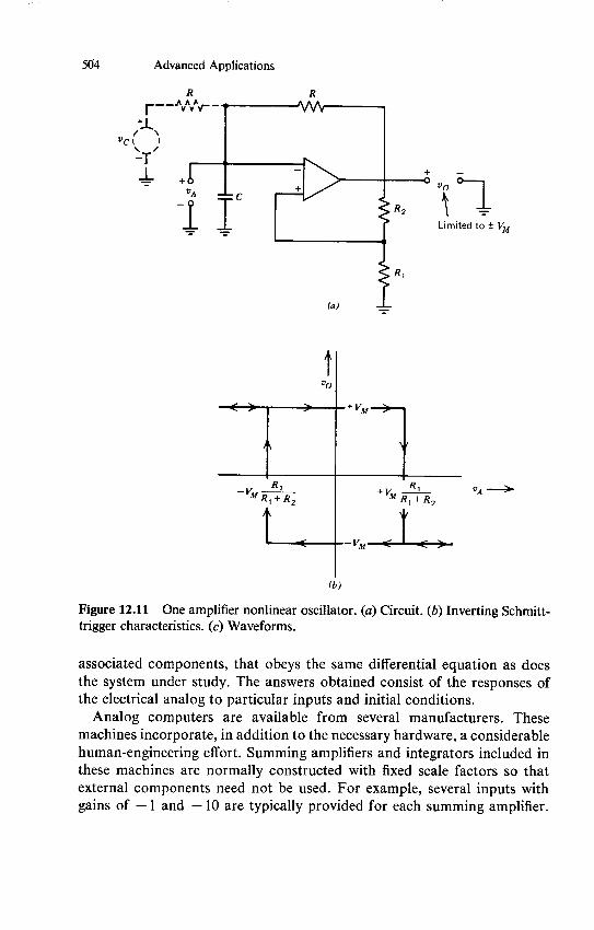
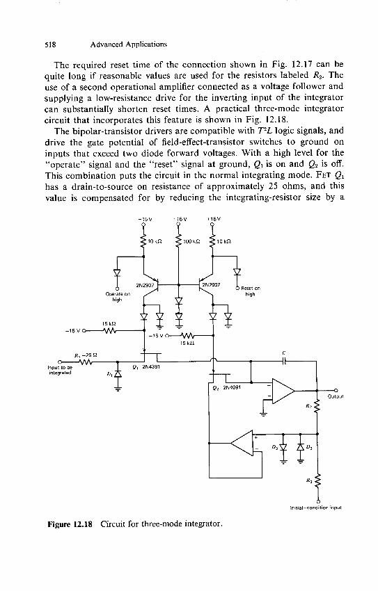
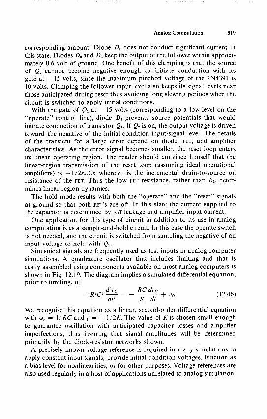
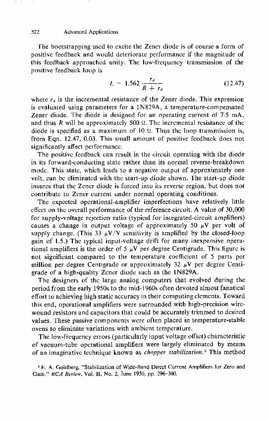
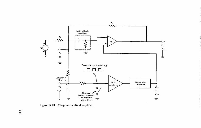

200 mV
I T
(a) 1 ms
200 mV
(b) 1 Ms
Figure 1229 Input and output signals for second-order Padd approximate to a 1-ms time delay (a) Sine-wave excitation (b) Triangular-wave excitation (c) Square-wave excitation
534
535 Active Filters
200 mV
I T
(c) 1 ms
Figure 1229-Continued
input and output signals for 100-Hz sine-wave excitation are shown in Fig 1229a The time delay between these two signals is 1 ms to within instrushymentation tolerances This performance reflects the prediction of Fig 1227 since good agreement to 2000 radsec or 300 Hz is anticipated for the apshyproximation to a 1-ms delay
Input and output signals for 100-Hz triangular-wave excitation are comshypared in Fig 1229b The triangular wave contains only odd harmonics and these harmonics fall off as the square of their frequency Thus the amplitude of the third harmonic of the triangular wave is approximately 11 of the amplitude of the fundamental the amplitude of the fifth harmonic is 4 of the fundamental while higher harmonics are further attentuated We notice that the circuit does very well in approximating a 1-ms time delay most of the time The aberration that results immediately following a change in slope reflects the inability of the circuit to provide proper phase shift to the higher-frequency components
The performance of the circuit when excited with an 100-Hz square wave is shown in Fig 1229c The relatively poorer behavior in the vicinity of a transition in this case results from the higher harmonic content of the square wave (Recall that the square wave contains odd harmonics that fall off only as the first power of the frequency)
536 Advanced Applications
125 FURTHER EXAMPLES
It was mentioned in the introduction to Chapter 11 that the objective of
the application portion of this book was to illustrate concepts for design
rather than to provide specific detailed examples in the usually futile
hope that the reader could apply them directly to his own problems
Successful design almost always involves combining bits and pieces a
concept here a topology there to ultimately arrive at the optimum solution
In this section we will see how some of the ideas introduced earlier are
combined into relatively more sophisticated configurations The three
examples that are presented are all real world in that they reflect actual
requirements that the author has encountered recently in his own work
1251 A Frequency-Independent Phase Shifter
There are a number of operational-amplifier connections such as the
approximation to a time delay described in the previous section that have
a transfer-function magnitude independent of frequency combined with
specified phase characteristics The phase shifter shown in Fig 1230 is
another example of this type of circuit We recognize this circuit as a differshy
ential-amplifier connection and thus realize that its transfer function is
V__s = 2RCsRs-1V0(s) = _2RC - 1 = RCs -1 (1269) Vi(s) RCs + 1 RCs + 1
This transfer function (which is the negative of a first-order Pade approxishy
mate to a time delay of 2RC seconds) produces a phase shift that varies from
- 1800 at low frequencies to 0 at high frequencies If a potentiometer or a
field-effect transistor is used for R the phase shift can be manually or
electronically varied
R1
R1
+ c RVi n
Figure 1230 Adjustable phase shifter
537 Further Examples
Input sinusoid Output sinusoid
shifter
Integrator
multiplier
Figure 1231 Constant phase shifter using a phase detector
One technique for converting resolver8 signals to digital form requires that a fixed 900 phase shift be applied to a sinusoidal signal with no change in its amplitude The frequency of the signal to be phase shifted may change by a few percent Unfortunately there are no finite-polynomial linear transfer functions that combine frequency-independent magnitude characshyteristics with a constant 900 phase shift While approximating functions do exist over restricted frequency ranges the arc-minute phase-shift constancy required in this application precluded the use of such functions We note that since a very specific class of input signals (single-frequency sinusoids) is to be applied to the phase shifter linearity may not be a necessary conshystraint Nonlinear circuits in spite of our inability to analyze them systeshymatically often have very interesting properties
Consider the configuration shown diagrammatically in Fig 1231 as a possible solution to our problem In this circuit an all-pass phase shifter with a voltage-variable amount of phase shift is the central element The circuit shown in Fig 1230 with a field-effect transistor used for the resistor R can perform this function The multiplier is used as a phase detector If the magnitude of the phase shift between the input and output signals is less than 900 the average value of the multiplier output will be positive while if this magnitude is between 90 and 1800 the average multiplier outshyput signal will be negative The integrator which provides the control
8 A resolver is basically a transformer with a primary-to-secondary coupling that can be varied by mechanically changing the relative alignment of these windings This device is used as a rugged and highly accurate mechanical-angle transducer
538 Advanced Applications
voltage for the FET in the phase shifter filters the second harmonic that results from the multiplication and supplies the loop gain necessary to keep the average value of the multiplier output at zero thus forcing a 900 phase shift between input and output signals Although the circuit described above can result in moderate accuracy a detailed investigation indicated that meeting the required specifications probably was not practical with this topology
It is worth noting that while the basic approach described above was not used in this case it is a valuable technique that has a number of interesting and useful variations For example the phase shift of a second-order high-or low-pass active filter is plusmn90 when excited at its corner frequency Tracking filters can be realized by replacing the fixed resistors in an active filter with voltage-controlled resistors and using a phase comparison to locate the corner frequency of the filter at its excitation frequency
In some applications other types of phase detectors are used One possishybility involves high-gain limiters that produce square waves with zero crossshying synchronized to those of the sine waves of interest The duty cycle of an exclusive OR gate operating on the square waves indicates the relative phase of the original signals
The previous circuit combined an all-pass network that provides a transfer-function magnitude that is independent of frequency with feedback which forces 90 of phase shift at the operating frequency An alternative approach is to combine a network that provides 90 of phase shift at all frequencies (an integrator) with feedback that forces its gain magnitude to be one at the operating frequency
The circuit that evolved to implement the above concept is shown in only slightly simplified form in Fig 1232 The signal integrator provides the required 90 of phase shift Its scale factor is adjusted by means of the field-effect transistor so that a gain magnitude of one is provided at frequencies close to the nominal operating value of 400 Hz Half of the drain-to-source voltage of the field-effect transistor is applied to its gate to linearize the drain-to-source resistance as described in Section 1214 The unity-gain buffer amplifier prevents current flowing through the FET-gate network from being integrated The capacitor in series with the signal-integrator input reshysistor and the resistor shunting the integrating capacitor are required to keep this integrator from saturating as a consequence of input voltage offset and bias current While they change the ideal phase shift by a total of approxishymately eight arc minutes this value is trimmed out along with other phase-shift errors with a network (not shown) following the integrator
The two full-wave precision-rectifier connections combine with the loop-gain integrator to provide an average current into the capacitor of this
0039 yF
Input (400 Hz)
375 kS2
U
Figure 1232 Precision phase shifter with amplitude control
540 Advanced Applications
integrator that is proportional to the difference between the magnitudes of
the input and output signals If for example the output-signal magnitude
exceeds the input-signal magnitude the voltage out of the loop-gain inteshy
grator is driven negative This action increases the incremental resistance
of the FET thus decreasing the signal-integrator scale factor and lowering
the magnitude of the output signal The inputs to the precision rectifiers are
a-c coupled so that d-c components of these signals do not influence the
rectifier output signals A two-pole low-pass filter follows the loop-gain
integrator to further filter harmonics that would degrade signal-integrator
performance The maximum positive output level of the loop-gain integrator is clamped
via an internal node to a maximum output level of zero volts in order to
eliminate a latch-up mode If this voltage became positive the FET would
conduct gate current and this current could cause the signal-integrator
output to saturate As a result the a-c component of the signal-integrator
output would be eliminated and the loop in an attempt to restore equishy
librium would drive the output of the loop-gain integrator further positive
The diode clamp prevents initiation of this unfortunate chain of events
The circuit shown in Fig 1232 has been built and tested at operating
frequencies between 395 and 405 Hz over the temperature range of 00 to
50 Centigrade (The feedback also eliminates the effects of signal-integrator
component-value changes with temperature) The input- and output-signal amplitudes remain equal within I mV peak-to-peak at any input-signal
level up to 20 volts peak-to-peak The phase shift of the circuit with a 20shy
volt peak-to-peak input remains constant within one arc minute While the
actual phase shift is not precisely 90 the constant component of the phase
error can be trimmed out as described earlier
1252 A Sine-Wave Shaper
We have discussed certain aspects of a function-generator circuit that
combines an integrator and a Schmitt trigger to produce square and triangle
waves in Sections 633 and 1221 Commercial versions of this circuit
usually also provide a sine-wave output that is synthesized by the seemingly
improbable method of shaping the triangle wave with a piecewise-linear
network This technique is practical because of the ease of generating
variable-frequency triangular waves and because the use of relatively few
segments in the shaping network gives surprisingly good sine-wave fidelity
Part of the design problem is to determine how the characteristics of the
shaping network should be chosen to best approximate a sine wave The
parameters that define the network are shown in Fig 1233 A total of n
break points are located over the input-variable range of 00 to 90 The
541 Further Examples
Slope = KS
-90 -on 61 62 on 900 0
SI
Slope = KS
Figure 1233 Piecewise-linear network characteristics
slope of the input-output transfer relationship is KSm between 0 = 0m and
o = 6m+1 The multiplying constant K reflects the fact that only relative slopes are important since a multiplicative change in all slopes changes only the magnitude of the input-output transfer characteristics The symshy
metry of the transfer characteristics about the origin insures that the output signal will have no d-c component and will contain no even harmonics when a zero-average-value triangular signal is used as the input
The network specification involves the choice of n values of 0 (the breakshypoint locations) and n + 1 relative slopes It can be shown that if the Os
are selected such that
m 1800 Om = M 80 0 lt M lt n7 (1270)
2n + 1 shy
and slopes selected as
Sm = sin 0m+1 - sin Om 0 lt m lt n (1271a)
Sm= 0 m = n (1271b)
the first n odd harmonics will be eliminated from the output signal
The decision to use four break points in the realization of the sine shaper was based on two considerations With this number of break points outshy
542 Advanced Applications
put distortion resulting from imprecise break-point locations and slope values is comparable to the distortion associated with the piecewise-linear approximation unless expensive components are used to establish these parameters Furthermore an inexpensive integrated-circuit five-diode array is available This matched-diode array can be used for the four break points with the fifth diode providing temperature compensation as described in material to follow Equations 1270 and 1271 evaluated for n - 4 suggest break points located at input-variable values of 20 400 60 and 800 with relative segment slopes (normalized to a minimum nonzero slope of one) of 2879 2532 1879 1 and 0 respectively
With the transfer characteristics of the shaping network determined it is necessary to design the circuit that synthesizes the required function The discussion of Section 1153 mentioned the use of superdiode connections to improve the sharpness of break points compared to that which can be achieved with diodes alone This technique was not used for the sine shaper since the rounding associated with the normal diode forward characteristics actually improves the quality of the fit to the sine curve
The compressive type nonlinearities described in Section 1153 were realized using diodes to increase the feedback around an operational amplifier thus reducing its incremental closed-loop gain when a breakshypoint level was exceeded An alternative is to use diodes to decrease the drive signal applied to the amplifier to lower incremental gain This apshyproach simplifies temperature compensation The topology used is shown in Fig 1234
The input-signal level of 20 volts peak-to-peak corresponds to the input variable range of z90 shown in Fig 1233 Thus the break-point locashytions of L20 plusmn40 -60 and L800 correspond to input-voltage levels of plusmn222 volts plusmn444 volts plusmn667 volts and plusmn-+89 volts respectively Resistor values are determined as follows It is initially assumed that the diodes are ideal in that they have a threshold voltage of zero volts zero resistance in the forward direction and zero conductance in the reverse direction Assume that the R1-R2 path is to provide the break points at input voltages of plusmn 889 volts Since the inverting input of the operational amplifier is at ground potential the resistor ratio necessary to make the voltage at the midpoint of these two resistors plusmn 15 volts with plusmn 889 volts at the input is
R215 R2 1 5 = 01687 (1272)
R1 + R2 889
The ratios of resistor pairs R3-R 4 R5-R6 and RrRs are chosen in a similar way to locate the remaining break points
+10 V--shy
OA
-10 V------shy
Signal v
v +
+1
+ O -
Figure 1234 Simplified sine-wave shaper
544 Advanced Applications
The relative conductances of the resistive paths between the triangular-wave signal source and the inverting input of the operational amplifier are constrained by the relative slopes of the desired transfer characteristics as follows The closed-loop incremental gain of the connection is proportional to the incremental transfer conductance from the signal source to the current iA defined in Fig 1234 With the ratio of the two resistors in each path chosen in accordance with relationships like Eqn 1272 the increshymental transfer conductance is zero (for ideal diodes) when the input-signal magnitude exceeds 889 volts increases to 1(R1 + R 2) for input-signal magnitudes between 667 and 889 volts increases further to [1(R 1 + R 2)] + [1(R 3 + R 4)] for input-signal magnitudes between 444 and 667 volts etc If we define 1(R1 + R2 ) = G realizing the correct relative slope for input-signal magnitudes between 444 and 667 volts reshyquires
1 1 2 = 1S79G (1273)R +R 2 R 3 -+FR 4
The satisfaction of Eqn 1273 makes the slope in this input signal range 1879 times as large as the slope for input signals between 667 and 889 volts Corresponding relationships couple other resistor-pair values to the R1 -R 2 pair
The sets of equations that parallel Eqns 1272 and 1273 together with the selection of any one resistor value determine reistors R1 through R 8 The general resistance level set by choosing the one free resistor value is selected based on loading considerations and to insure that stray capacitance does not deteriorate dynamic performance
The circuit used for the sine shaper (Fig 1235) uses the standard 17oshytolerance resistor values that best approximate calculated values The five diodes labeled A and those labeled B are from two CA3039 integrated-circuit diode arrays One member of each array modifies the bias voltages to account for the diode threshold voltages and to provide temperature compensation The compensating diodes are operated at a current level of approximately half the maximum operating current level of the shaping diodes While this type of compensation clearly has no effect on the conshyductance characteristics of the shaping diodes the exponential diode characshyteristics actually improve the performance of the circuit as described earlier
Since this circuit is intended to operate to 1 MHz (a high-speed integrated-circuit operational amplifier with a discrete-component buffer to increase output-current capacity is used) capacitors are necessary at the output of the reference-voltage amplifiers to lower their output impedance at the switching frequency of the diodes The 15-V levels are derived from the
Triangle-wave D - t 78 2k input ~ - -r4I (20-volt peak-peak) OtuOtu
Figure 1235 Sine-wave shaper
546 Advanced Applications
200 Ts
Figure 1236 Output from sine-wave shaper
voltages that establish triangle-wave amplitude so that any changes in this
amplitude cause corresponding break-point location changes
The circuit produces approximate sine waves with the amplitude of any individual harmonic in the output signal at least 40 dB (a voltage ratio of 1001) below the fundamental This performance is obtained with no trimming If adjustments are made to null the offset of the operational
amplifier and empirical adjustments (guided by a spectrum analyzer) are
used to counteract component-value errors and to compensate for finite diode forward resistance the amplitude of individual output-signal harmonics can be reduced to 55 dB below the fundamental at low frequenshycies Performance deteriorates somewhat at frequencies above approxishy
mately 10 kHz because of reduced signal-amplifier open-loop gain
A 1-kHz output signal from the circuit is shown in Fig 1236
1253 A Nonlinear Three-Port Network
The realization of a device analog that may be of value in teaching the dynamic behavior of bipolar transistors requires a three-port network
547 Further Examples
VB E
VE - N
Figure 1237 Three-port network
defined by Fig 1237 The synthesis of this network is initiated by first
designing a circuit that provides the relationship
VN = VB - V0 exp [(VB- VE) (1274)
The parameter Vo as we might expect is related to the quantity Is for the
transistor being simulated and consequently a corresponding temperature
dependence is desirable There are a number of ways to simulate Eqn 1274 One topology that
is adaptable to further requirements is shown in Fig 1238 Since an evenshy
tual constraint is that the current at the VB input be zero a buffer amplifier
is used at this terminal The second amplifier is differentially connected
with an output voltage
VA = 2VE - VB (1275)
The third amplifier is also connected as a differential amplifier so that
VN = VE - (iT + iA)R (1276)
Since feedback keeps the inverting input terminal of the third amplifier at
potential VE
A A - VE VE -B (177)R R
00
+ vc
IT R
VB
+ VB
+N
VA
-I
VE
Figure 1238 Synthesis of exponential relationship
549 FurtherExamples
If we assume the usual transistor characteristics
ir Is jexp [(VB- 1i (1278)
Substituting Eqns 1277 and 1278 into Eqn 1276 yields the form reshyquired by Eqn 1275
VN = VB - RIs exp VE)] -(VB- (1279)
In order to complete the synthesis it is necessary to sample the current flowing at terminal N and make the current flowing at terminal E the negashytive of this current A modification of the Howland current source (see Section 1143) can be used The basic circuit with differential inputs is shown in Fig 1239a (The reason for the seemingly strange input-voltage connection and the split resistor will become apparent momentarily) The current io for these parameter values is
22 (VA - vc) (VA - VA - vr) -2vr
o - (1280)R R R
In Fig 1239b the voltage source vr and half of the split resistor are reshyplaced with a Norton-equivalent circuit For equivalence it is necessary to make ir = 2vrR Expressing Eqn 1280 in terms of ir shows
io = -i (1281)
The topology of Fig 1239b shows that the iT current source can be reshyturned to ground rather than to voltage source VA This modification is shown in Fig 1239c the current-controlled current source necessary in our present application Note that the output is independent of VA the common-mode input voltage applied to the current source
The circuits of Figs 1238 and 1239c are combined to form the three-port network as shown in Fig 1240 In this circuit the feedback for the voltage vN is taken from the output side of the current-sampling resistor so that voltage drops in this resistor do not influence vN It is necessary to buffer the 100-kQ feedback resistor with a unity-gain follower to insure that current through this resistor does not flow through the current-sampling resistor and thus alter iE
The trim potentiometer allows precise matching of resistor ratios to make current iE independent of common-mode voltage levels at various points in the current source and thus dependent only on iN In this applicashytion it was not necessary to have exactly unity gain between iN and - iE so no trim is included for this ratio The general magnitude of the resistors
2R
R
VI
VA
(a)
2R
R
VA 1
i~ (b)
R 2R 1
R R 2 2 +
VA i A
R R
- R Load
o -
(c) Figure 1239 Current-controlled current source (a) Basic Howland current source (b) Current source following Norton substitution (c) Final configuration
550
I
Problems 551
VB
+ L- I----oVE 0-1249 k 2 249 k2 499 k E2 7j
100 k2
Figure 1240 Complete nonlinear three-port network
in the current source is chosen for compatibility with required current levels and amplifier characteristics and is not important for purposes of this discussion
PROBLEMS
P121 Consider a Wien-Bridge oscillator as shown in Fig 121 Show that if
the output signal is of the general form vo = E sin [(tRC) + 0] where 0 is a constant the signals applied to the two inputs of the operational amplishyfier are virtually identical a necessary condition for satisfactory performshyance Note that if the inverting and noninverting inputs are interchanged and it is assumed that the output has the form indicated above the signals at the two inputs will also be identical However this modified topology will not function as an oscillator Explain
P122 A Wien-Bridge oscillator is constructed using the basic topology shown
in Fig 121 Because of component tolerances the time constants of the series and parallel arms of the frequency-dependent feedback network
552 Advanced Applications
differ by 5 How must component values in the frequency-independent feedback path be related to guarantee oscillation
P123 Use a describing-function approach to analyze the circuit shown in Fig
123 assuming that the operational amplifier is ideal and that the diodes have zero conductance until a forward voltage of 06 volt is reached and zero resistance in the forward-conducting state In particular determine the magnitude of the signal applied to the noninverting input of the amplifier and the third-harmonic distortion present at the amplifier output
P124 A sinusoidal oscillator is constructed by connecting the output of a
double integrator (see Fig 1112) to its input Show that amplitude can be controlled by varying the magnitude of the (R2)-valued resistor shown in this figure Design a complete circuit that can produce a 20-V peak-to-peak output signal at 1 kHz Use a FET with parameters given in Section 1214 for the control element Analyze your amplitude-control loop to show that it has acceptable stability and a crossover frequency compatible with the 1-kHz frequency of oscillation If you have confidence in your design build it The 2N4416 field-effect transistor is reasonably well characterized by the parameters referred to above
P125 The discussions of Sections 1222 and 1223 suggest operating electronic
switches connected to symmetrical variable voltages from the output of a
t +v F
VIshy
_VF
Figure 1241 Infinite-gain limiter
Problems 553
Schmitt trigger for two different applications An alternative to the use of
switches is to use a circuit that has the transfer characteristic shown in
Fig 1241 for the necessary shaping function (In this diagram the voltage
VF is a positive variable) Design a circuit that uses operational amplifiers
to synthesize this transfer characteristic Your output levels should be
insensitive to temperature variations
P126
A magnetic-suspension system was described in Section 623 Develop
an electronic analog simulation of this system that permits determination
of the transients that result from disturbing forces applied to the ball
Assume that in addition to operational amplifiers and appropriate passive
components multipliers with a scale factor vo = vxvy 10 volts are available
A way to perform the division required in this simulation using a multishy
plier and an operational amplifier is outlined in Section 622 You may leave the various element values in the simulation defined in
terms of system parameters without developing final amplitude-scaled values
P127
A circuit intended for use as a precision voltage reference for an analog-
to-digital converter is shown in Fig 1242 The circuit uses a fraction of the
Zener-diode voltage as its output While this method involving resistive
attenuation results in relatively high output resistance compared with using
the voltage at the output of the amplifier as the reference the output
voltage becomes essentially independent of operational-amplifier offset voltage
R1
1N4779A- +
9 k2
Figure 1242 Voltage reference
554 Advanced Applications
C1
R R
Vi +
C2 R +I Ri
Figure 1243 Low-pass Sallen and Key circuit with voltage gain
The specified breakdown voltage of the 1N4779A is 85 volts 5 The indicated resistor is selected during testing to obtain the required output voltage independent of the actual value of the Zener-diode voltage
The breakdowh voltage range and the temperature coefficient of the device are guaranteed at an operating current of 0500 mA By proper choice of R1 and R 2 it is possible to make the current through the Zener diode independent of the actual Zener voltage after the single indicated selection has been completed Such a choice is advantageous since it simshyplifies circuit calibration as opposed to methods that require two or more
interdependent adjustments to set output voltage and Zener-diode operatshying current Find values for R1 and R 2 that result in this simplification (Please excuse the somewhat unwieldy numbers involved in this problem but it is drawn directly from an existing application)
P128 A Sallen and Key low-pass circuit with an amplifier closed-loop voltage
gain greater than unity is shown in Fig 1243 Determine the transfer function V 0(s)Vi(s) for this circuit Compare the sensitivity of this circuit to component variations with that of the unity-gain version
P129
One way to analyze the Sallen and Key circuit shown in Fig 1243 is to
recognize the configuration as a positive-feedback circuit If the loop is
broken at the noninverting input to the operational amplifier analysis
techniques based on loop-transmission properties can be used
(a) Indicate the loop-transmission singularity pattern that results when the
loop is broken at the point mentioned above It is not necessary to determine singularity locations exactly in terms of element values
Problems 555
(b) Show how the closed-loop poles of the system move as a function of the closed-loop gain of the operational amplifier by using root-locus methods that have been appropriately modified for positive feedback systems
P1210 Design a sixth-order Butterworth filter with a 1 kHz corner frequency
by cascading three unity-gain Sallen and Key circuits
P1211 The fifth-order Pad6 approximate to a one-second time delay is
1 - 05s + 0111s 2 - 139 X 10-2 s3
+ 992 X 10- 4s4 - 331 X 10- 5s5
1 + 05s + 0111s2 - 139 X 10- 2s3
+ 992 X 10- 4s4 + 331 X 10- 5s
Design an active filter that synthesizes this transfer function
P1212 Develop a linearized block-diagram for the system shown in Fig 1232
assuming that the FET is characterized by the parameters given in Section 1214 Show that the loop crossover frequency is low compared to 400 Hz for any input-voltage level up to 20 volts peak-to-peak Estimate the time required for the system to restore equilibrium following an incremental perturbation (initiated for example by a change in input frequency) when the input-signal amplitude is 100 mV peak-to-peak Note that the system is not significantly disturbed by a change in input amplitude when operating under equilibrium conditions and that therefore this relatively long settling time does not deteriorate performance
MIT OpenCourseWarehttpocwmitedu
RES6-010 Electronic Feedback SystemsSpring 2013
For information about citing these materials or our Terms of Use visit httpocwmiteduterms
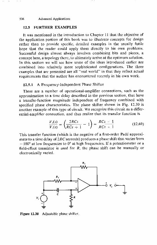

2R
R
VI
VA
(a)
2R
R
VA 1
i~ (b)
R 2R 1
R R 2 2 +
VA i A
R R
- R Load
o -
(c) Figure 1239 Current-controlled current source (a) Basic Howland current source (b) Current source following Norton substitution (c) Final configuration
550
I
Problems 551
VB
+ L- I----oVE 0-1249 k 2 249 k2 499 k E2 7j
100 k2
Figure 1240 Complete nonlinear three-port network
in the current source is chosen for compatibility with required current levels and amplifier characteristics and is not important for purposes of this discussion
PROBLEMS
P121 Consider a Wien-Bridge oscillator as shown in Fig 121 Show that if
the output signal is of the general form vo = E sin [(tRC) + 0] where 0 is a constant the signals applied to the two inputs of the operational amplishyfier are virtually identical a necessary condition for satisfactory performshyance Note that if the inverting and noninverting inputs are interchanged and it is assumed that the output has the form indicated above the signals at the two inputs will also be identical However this modified topology will not function as an oscillator Explain
P122 A Wien-Bridge oscillator is constructed using the basic topology shown
in Fig 121 Because of component tolerances the time constants of the series and parallel arms of the frequency-dependent feedback network
552 Advanced Applications
differ by 5 How must component values in the frequency-independent feedback path be related to guarantee oscillation
P123 Use a describing-function approach to analyze the circuit shown in Fig
123 assuming that the operational amplifier is ideal and that the diodes have zero conductance until a forward voltage of 06 volt is reached and zero resistance in the forward-conducting state In particular determine the magnitude of the signal applied to the noninverting input of the amplifier and the third-harmonic distortion present at the amplifier output
P124 A sinusoidal oscillator is constructed by connecting the output of a
double integrator (see Fig 1112) to its input Show that amplitude can be controlled by varying the magnitude of the (R2)-valued resistor shown in this figure Design a complete circuit that can produce a 20-V peak-to-peak output signal at 1 kHz Use a FET with parameters given in Section 1214 for the control element Analyze your amplitude-control loop to show that it has acceptable stability and a crossover frequency compatible with the 1-kHz frequency of oscillation If you have confidence in your design build it The 2N4416 field-effect transistor is reasonably well characterized by the parameters referred to above
P125 The discussions of Sections 1222 and 1223 suggest operating electronic
switches connected to symmetrical variable voltages from the output of a
t +v F
VIshy
_VF
Figure 1241 Infinite-gain limiter
Problems 553
Schmitt trigger for two different applications An alternative to the use of
switches is to use a circuit that has the transfer characteristic shown in
Fig 1241 for the necessary shaping function (In this diagram the voltage
VF is a positive variable) Design a circuit that uses operational amplifiers
to synthesize this transfer characteristic Your output levels should be
insensitive to temperature variations
P126
A magnetic-suspension system was described in Section 623 Develop
an electronic analog simulation of this system that permits determination
of the transients that result from disturbing forces applied to the ball
Assume that in addition to operational amplifiers and appropriate passive
components multipliers with a scale factor vo = vxvy 10 volts are available
A way to perform the division required in this simulation using a multishy
plier and an operational amplifier is outlined in Section 622 You may leave the various element values in the simulation defined in
terms of system parameters without developing final amplitude-scaled values
P127
A circuit intended for use as a precision voltage reference for an analog-
to-digital converter is shown in Fig 1242 The circuit uses a fraction of the
Zener-diode voltage as its output While this method involving resistive
attenuation results in relatively high output resistance compared with using
the voltage at the output of the amplifier as the reference the output
voltage becomes essentially independent of operational-amplifier offset voltage
R1
1N4779A- +
9 k2
Figure 1242 Voltage reference
554 Advanced Applications
C1
R R
Vi +
C2 R +I Ri
Figure 1243 Low-pass Sallen and Key circuit with voltage gain
The specified breakdown voltage of the 1N4779A is 85 volts 5 The indicated resistor is selected during testing to obtain the required output voltage independent of the actual value of the Zener-diode voltage
The breakdowh voltage range and the temperature coefficient of the device are guaranteed at an operating current of 0500 mA By proper choice of R1 and R 2 it is possible to make the current through the Zener diode independent of the actual Zener voltage after the single indicated selection has been completed Such a choice is advantageous since it simshyplifies circuit calibration as opposed to methods that require two or more
interdependent adjustments to set output voltage and Zener-diode operatshying current Find values for R1 and R 2 that result in this simplification (Please excuse the somewhat unwieldy numbers involved in this problem but it is drawn directly from an existing application)
P128 A Sallen and Key low-pass circuit with an amplifier closed-loop voltage
gain greater than unity is shown in Fig 1243 Determine the transfer function V 0(s)Vi(s) for this circuit Compare the sensitivity of this circuit to component variations with that of the unity-gain version
P129
One way to analyze the Sallen and Key circuit shown in Fig 1243 is to
recognize the configuration as a positive-feedback circuit If the loop is
broken at the noninverting input to the operational amplifier analysis
techniques based on loop-transmission properties can be used
(a) Indicate the loop-transmission singularity pattern that results when the
loop is broken at the point mentioned above It is not necessary to determine singularity locations exactly in terms of element values
Problems 555
(b) Show how the closed-loop poles of the system move as a function of the closed-loop gain of the operational amplifier by using root-locus methods that have been appropriately modified for positive feedback systems
P1210 Design a sixth-order Butterworth filter with a 1 kHz corner frequency
by cascading three unity-gain Sallen and Key circuits
P1211 The fifth-order Pad6 approximate to a one-second time delay is
1 - 05s + 0111s 2 - 139 X 10-2 s3
+ 992 X 10- 4s4 - 331 X 10- 5s5
1 + 05s + 0111s2 - 139 X 10- 2s3
+ 992 X 10- 4s4 + 331 X 10- 5s
Design an active filter that synthesizes this transfer function
P1212 Develop a linearized block-diagram for the system shown in Fig 1232
assuming that the FET is characterized by the parameters given in Section 1214 Show that the loop crossover frequency is low compared to 400 Hz for any input-voltage level up to 20 volts peak-to-peak Estimate the time required for the system to restore equilibrium following an incremental perturbation (initiated for example by a change in input frequency) when the input-signal amplitude is 100 mV peak-to-peak Note that the system is not significantly disturbed by a change in input amplitude when operating under equilibrium conditions and that therefore this relatively long settling time does not deteriorate performance
MIT OpenCourseWarehttpocwmitedu
RES6-010 Electronic Feedback SystemsSpring 2013
For information about citing these materials or our Terms of Use visit httpocwmiteduterms

MIT OpenCourseWarehttpocwmitedu
RES6-010 Electronic Feedback SystemsSpring 2013
For information about citing these materials or our Terms of Use visit httpocwmiteduterms