ads 7834
DESCRIPTION
Datasheet of analog to digital converter 12 bits. Analog Devices.TRANSCRIPT

ADS7834
DESCRIPTIONThe ADS7834 is a 12-bit sampling analog-to-digital converter(A/D) complete with sample/hold, internal 2.5V reference,and synchronous serial interface. Typical power dissipationis 11mW at a 500kHz throughput rate. The device can beplaced into a power-down mode that reduces dissipation tojust 2.5mW. The input range is zero to the reference voltage,and the internal reference can be overdriven by an externalvoltage.
Low power, small size, and high speed make the ADS7834ideal for battery-operated systems such as wirelesscommunication devices, portable multi-channel data loggers,and spectrum analyzers. The serial interface also provideslow-cost isolation for remote data acquisition. The ADS7834is available in a plastic mini-DIP-8 or an MSOP-8 packageand is ensured over the –40°C to +85°C temperature range.
12-Bit High-Speed, Low-Power SamplingANALOG-TO-DIGITAL CONVERTER
FEATURES 500kHz THROUGHPUT RATE
2.5V INTERNAL REFERENCE
LOW POWER: 11mW
SINGLE-SUPPLY +5V OPERATION
DIFFERENTIAL INPUT
SERIAL INTERFACE
12-BITS NO MISSING CODES
MINI-DIP-8 AND MSOP-8
0V TO VREF INPUT RANGE
APPLICATIONS BATTERY-OPERATED SYSTEMS
DIGITAL SIGNAL PROCESSING
HIGH-SPEED DATA ACQUISITION
WIRELESS COMMUNICATION SYSTEMS
ADS7834
SARCLK
SerialInterface
ComparatorS/H Amp
DATA
+In
–InCDAC
Internal+2.5V Ref
Buffer
VREF
CONV
10kΩ ±30%
SBAS098A – JANUARY 1998 – REVISED SEPTEMBER 2003
www.ti.com
PRODUCTION DATA information is current as of publication date.Products conform to specifications per the terms of Texas Instrumentsstandard warranty. Production processing does not necessarily includetesting of all parameters.
Copyright © 1998-2003, Texas Instruments Incorporated
Please be aware that an important notice concerning availability, standard warranty, and use in critical applications ofTexas Instruments semiconductor products and disclaimers thereto appears at the end of this data sheet.
All trademarks are the property of their respective owners.

ADS78342SBAS098Awww.ti.com
1
2
3
4
8
7
6
5
+VCC
CLK
DATA
CONV
VREF
+IN
–IN
GND
ADS7834
MSOP-8
1
2
3
4
8
7
6
5
+VCC
CLK
DATA
CONV
VREF
+IN
–IN
GND
ADS7834
Plastic Mini-DIP-8
+VCC to GND ............................................................................–0.3V to 6VAnalog Inputs to GND .............................................. –0.3V to (VCC + 0.3V)Digital Inputs to GND ............................................... –0.3V to (VCC + 0.3V)Power Dissipation .......................................................................... 325mWMaximum Junction Temperature ................................................... +150°COperating Temperature Range ......................................... –40°C to +85°CStorage Temperature Range .......................................... –65°C to +150°CLead Temperature (soldering, 10s) ............................................... +300°C
NOTE: (1) Stresses above those listed under “Absolute Maximum Ratings” maycause permanent damage to the device. Exposure to absolute maximum condi-tions for extended periods may affect device reliability.
ELECTROSTATICDISCHARGE SENSITIVITY
Electrostatic discharge can cause damage ranging fromperformance degradation to complete device failure. TexasInstruments recommends that all integrated circuits be handledand stored using appropriate ESD protection methods.
ESD damage can range from subtle performance degrada-tion to complete device failure. Precision integrated circuitsmay be more susceptible to damage because very smallparametric changes could cause the device not to meetpublished specifications.
ABSOLUTE MAXIMUM RATINGS(1)
PIN CONFIGURATION
Top View
PIN NAME DESCRIPTION
1 VREF Reference Output. Decouple to ground with a 0.1µF ceramic capacitor and a 2.2µF tantalum capacitor.
2 +IN Noninverting Input.
3 –IN Inverting Input. Connect to ground or to remote ground sense point.
4 GND Ground.
5 CONV Convert Input. Controls the sample/hold mode, start of conversion, start of serial data transfer, type of serial transfer, and powerdown mode. See the Digital Interface section for more information.
6 DATA Serial Data Output. The 12-bit conversion result is serially transmitted most significant bit first with each bit valid on the rising edgeof CLK. By properly controlling the CONV input, it is possibly to have the data transmitted least significant bit first. See the DigitalInterface section for more information.
7 CLK Clock Input. Synchronizes the serial data transfer and determines conversion speed.
8 +VCC Power Supply. Decouple to ground with a 0.1µF ceramic capacitor and a 10µF tantalum capacitor.
PIN ASSIGNMENTS
PACKAGE/ORDERING INFORMATION
MAXIMUM MAXIMUMINTEGRAL DIFFERENTIALLINEARITY LINEARITY SPECIFIED
ERROR ERROR PACKAGE- PACKAGE TEMPERATURE PACKAGE ORDERING TRANSPORTPRODUCT (LSB) (LSB) LEAD DESIGNATOR(1) RANGE MARKING(2) NUMBER(3) MEDIA, QUANTITY
ADS7834E ±2 N/S(3) MSOP-8 DGK –40°C to +85°C C34 ADS7834E/250 Tape and Reel, 250ADS7834E " " " " " " ADS7834E/2K5 Tape and Reel, 2500ADS7834EB ±1 ±1 MSOP-8 DGK –40°C to +85°C C34 ADS7834EB/250 Tape and Reel, 250ADS7834EB " " " " " " ADS7834EB/2K5 Tape and Reel, 2500ADS7834P ±2 N/S(3) Plastic DIP-8 P –40°C to +85°C ADS7834P ADS7834P RailsADS7834PB ±1 ±1 " " " ADS7834PB ADS7834PB Rails
NOTE: (1) For the most current specifications and package information, refer to our web site at www.ti.com. (2) Performance Grade information is marked on thereel. (3) N/S = Not Specified, typical only. However, 12-Bits no missing codes is ensured over temperature.
ADS7834 3SBAS098A www.ti.com
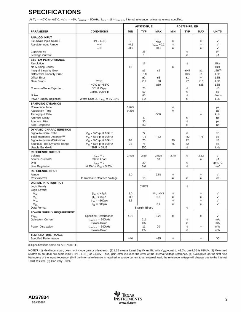
SPECIFICATIONS At TA = –40°C to +85°C, +VCC = +5V, fSAMPLE = 500kHz, fCLK = 16 • fSAMPLE, internal reference, unless otherwise specified.
ADS7834P, E ADS7834PB, EB
PARAMETER CONDITIONS MIN TYP MAX MIN TYP MAX UNITS
ANALOG INPUTFull-Scale Input Span(1) +IN – (–IN) 0 VREF VAbsolute Input Range +IN –0.2 VREF +0.2 V
–IN –0.2 +0.2 VCapacitance 25 pFLeakage Current 1 µA
SYSTEM PERFORMANCEResolution 12 BitsNo Missing Codes 12 BitsIntegral Linearity Error ±1 ±2 ±0.5 ±1 LSB(2)
Differential Linearity Error ±0.8 ±0.5 ±1 LSBOffset Error ±2 ±5 ±1 LSBGain Error(3) 25°C ±12 ±30 ±7 ±15 LSB
–40°C to +85°C ±50 ±35 LSBCommon-Mode Rejection DC, 0.2Vp-p 70 dB
1MHz, 0.2Vp-p 50 dBNoise 60 µVrmsPower Supply Rejection Worst Case ∆, +VCC = 5V ±5% 1.2 LSB
SAMPLING DYNAMICSConversion Time 1.625 µsAcquisition Time 0.350 µsThroughput Rate 500 kHzAperture Delay 5 nsAperture Jitter 30 psStep Response 350 ns
DYNAMIC CHARACTERISTICSSignal-to-Noise Ratio VIN = 5Vp-p at 10kHz 72 dBTotal Harmonic Distortion(4) VIN = 5Vp-p at 10kHz –78 –72 –82 –75 dBSignal-to-(Noise+Distortion) VIN = 5Vp-p at 10kHz 68 70 70 72 dBSpurious Free Dynamic Range VIN = 5Vp-p at 10kHz 72 78 75 82 dBUsable Bandwidth SNR > 68dB 350 kHz
REFERENCE OUTPUTVoltage IOUT = 0 2.475 2.50 2.525 2.48 2.52 VSource Current(5) Static Load 50 µADrift IOUT = 0 20 ppm /°CLine Regulation 4.75V ≤ VCC ≤ 5.25V 0.6 mV
REFERENCE INPUTRange 2.0 2.55 VResistance(6) to Internal Reference Voltage 10 kΩ
DIGITAL INPUT/OUTPUTLogic Family CMOS
Logic Levels:VIH |IIH| ≤ +5µA 3.0 VCC +0.3 VVIL |IIL| ≤ +5µA –0.3 0.8 VVOH IOH = –500µA 3.5 VVOL IOL = 500µA 0.4 V
Data Format Straight Binary
POWER SUPPLY REQUIREMENT+VCC Specified Performance 4.75 5.25 VQuiescent Current fSAMPLE = 500kHz 2.2 mA
Power-Down 0.5 mAPower Dissipation fSAMPLE = 500kHz 11 20 mW
Power-Down 2.5 mW
TEMPERATURE RANGESpecified Performance –40 +85 °C
Specifications same as ADS7834P,E.
NOTES: (1) Ideal input span, does not include gain or offset error. (2) LSB means Least Significant Bit, with VREF equal to +2.5V, one LSB is 610µV. (3) Measuredrelative to an ideal, full-scale input (+IN – (–IN)) of 2.499V. Thus, gain error includes the error of the internal voltage reference. (4) Calculated on the first nineharmonics of the input frequency. (5) If the internal reference is required to source current to an external load, the reference voltage will change due to the internal10kΩ resistor. (6) Can vary ±30%.

ADS78344SBAS098Awww.ti.com
SUPPLY CURRENT vs SAMPLE RATE
400100 600200 300 500
Sample Rate (kHz)
Supply
Curr
ent (m
A)
1.7
2.4
2.3
2.2
2.1
2.0
1.9
1.8
TYPICAL PERFORMANCE CURVESAt TA = +25°C, VCC = +5V, fSAMPLE = 500kHz, fCLK = 16 • fSAMPLE, and internal +2.5V reference, unless otherwise specified.
FULL-SCALE ERROR vs TEMPERATURE
20–40 100–20 0 40
Temperature (°C)
Del
ta fr
om +
25°C
(LS
B)
1
0
–1
–2
–3
–4
–5
–6
–7
–860 80
OFFSET VOLTAGE vs TEMPERATURE
–40 100–20 0 20 40
Temperature (°C)
Del
ta fr
om +
25°C
(LS
B)
0.5
0.4
0.3
0.2
0.1
0
–0.1
–0.2
–0.360 80
POWER-DOWN SUPPLY CURRENTvs TEMPERATURE
20–40 100–20 0 40
Temperature (°C)
Pow
er-d
own
Sup
ply
Cur
rent
(µA
)
390
470
440
430
420
410
400
450
460
60 80
SUPPLY CURRENT vs TEMPERATURE
20–40 100–20 0 40
Temperature (°C)
Sup
ply
Cur
rent
(m
A)
1.6
2.3
2.1
2.0
1.9
1.8
1.7
2.2
60 80
fSAMPLE
= 500kHz
fSAMPLE
= 125kHz
INTEGRAL LINEARITY and DIFFERENTIAL LINEARITYvs SAMPLE RATE
300100 600200 400
Sample Rate (kHz)
Del
ta fr
om f S
AM
PLE
= 5
00kH
z (L
SB
)
0.06
0.04
0.02
0
–0.02
–0.04
–0.06
–0.08
–0.1500
Change in IntegralLinearity (LSB)
Change in DifferentialLinearity (LSB)

ADS7834 5SBAS098A www.ti.com
FREQUENCY SPECTRUM(4096 Point FFT; fIN = 9.77kHz, –0.2dB)
Frequency (kHz)
0
–20
–40
–60
–80
–100
–120
Am
plitu
de (
dB)
0 50 100 150 200 250
TYPICAL PERFORMANCE CURVES (Cont.)At TA = +25°C, VCC = +5V, fSAMPLE = 500kHz, fCLK = 16 • fSAMPLE, and internal +2.5V reference, unless otherwise specified.
FULL-SCALE ERRORvs EXTERNAL REFERENCE VOLTAGE
External Reference Voltage (V)
0.300
0.200
0.100
0.000
–0.100
–0.200
–0.300
–0.400
–0.500
–0.600
Del
ta fr
om V
RE
F =
2.5
V (
mV
)
2.0 2.1 2.2 2.3 2.4 2.5
FREQUENCY SPECTRUM(4096 Point FFT; fIN = 977Hz, –0.2dB)
Frequency (kHz)
0
–20
–40
–60
–80
–100
–120
Am
plitu
de (
dB)
0 50 100 150 200 250
PEAK-TO-PEAK NOISEvs EXTERNAL REFERENCE VOLTAGE
2.22 2.52.1 2.3
External Reference Voltage (V)
Pea
k-to
-Pea
k N
oise
(LS
B)
0.90
0.85
0.80
0.75
0/70
0.65
0.60
0.55
0.502.4
POWER SUPPLY REJECTIONvs POWER SUPPLY RIPPLE FREQUENCY
1 1M10 100 1k
Power Supply Ripple Frequency (Hz)
Pow
er S
uppl
y R
ejec
tion
(mV
/V)
30
25
20
15
10
5
010k 100k
OFFSET VOLTAGE vs EXTERNALREFERENCE VOLTAGE
External Reference Voltage (V)
0.2
0.1
0
–0.1
–0.2
–0.3
–0.4
–0.5
–0.6
–0.7
–0.8
Del
ta fr
om V
RE
F =
2.5
V (
mV
)
2.0 2.2 2.4 2.55

ADS78346SBAS098Awww.ti.com
FREQUENCY SPECTRUM(4096 Point FFT; fIN = 99.7kHz, –0.2dB)
Frequency (kHz)
0.00
–20
–40
–60
–80
–100
–120
Am
plitu
de (
dB)
0 50 100 150 200 250
TYPICAL PERFORMANCE CURVES (Cont.)At TA = +25°C, VCC = +5V, fSAMPLE = 500kHz, fCLK = 16 • fSAMPLE, and internal +2.5V reference, unless otherwise specified.
SIGNAL-TO-NOISE RATIO andSIGNAL-TO-(NOISE+DISTORTION)
vs INPUT FREQUENCY
Input Frequency (kHz)
76
74
72
70
68
66
64
62
60
SN
R a
nd S
INA
D (
dB)
1 10 100 1000
SINAD
SNR
SPURIOUS FREE DYNAMIC RANGE and TOTAL HARMONIC DISTORTION
vs INPUT FREQUENCY
Input Frequency (kHz)
95
90
85
80
75
70
65
60
55
50
–95
–90
–85
–80
–75
–70
–65
–60
–55
–50
SF
DR
(dB
)
TH
D (
dB)
1 10 100 1000
THD
SFDR
First nine harmonicsof an input frequency
SIGNAL-TO-NOISE andSIGNAL-TO-(NOISE+DISTORTION)
vs TEMPERATURE
20–40 80 100–20 0 40
Temperature (°C)
SN
R a
nd S
INA
D D
elta
from
+25
°C (
dB) 0.3
0.2
0.1
0.
–0.1
–0.2
–0.3
–0.4
–0.560
fIN = 10kHz, –0.2dB)
SINAD
SNR

ADS7834 7SBAS098A www.ti.com
1
2
3
4
8
7
6
5
+VCC
CLK
DATA
CONV
VREF
+IN
–IN
GND
ADS7834 0.1µF
+5V
0.1µF 10µF
Serial ClockfromMicrocontrolleror DSP
Serial Data
Convert Start
+2.2µF
+
0V to 2.5VAnalog Input
FIGURE 1. Basic Operation of the ADS7834.
THEORY OF OPERATIONThe ADS7834 is a high-speed. successive approximationregister (SAR) analog-to-digital converter (A/D) with aninternal 2.5V bandgap reference. The architecture is basedon capacitive redistribution which inherently includes asample/hold function. The converter is fabricated on a 0.6µCMOS process. See Figure 1 for the basic operating circuitfor the ADS7834.
The ADS7834 requires an external clock to run the conver-sion process. This clock can vary between 200kHz (12.5kHzthroughput) and 8MHz (500kHz throughput). The duty cycleof the clock is unimportant as long as the minimum HIGHand LOW times are at least 50ns and the clock period is atleast 125ns. The minimum clock frequency is set by theleakage on the capacitors internal to the ADS7834.
The analog input is provided to two input pins: +IN and –IN.When a conversion is initiated, the differential input on thesepins is sampled on the internal capacitor array. While aconversion is in progress, both inputs are disconnected fromany internal function.
The range of the analog input is set by the voltage on theVREF pin. With the internal 2.5V reference, the input rangeis 0V to 2.5V. An external reference voltage can be placedon VREF, overdriving the internal voltage. The range for theexternal voltage is 2.0V to 2.55V, giving an input voltagerange of 2.0V to 2.55V.
The digital result of the conversion is provided in a serialmanner, synchronous to the CLK input. The result is pro-vided most significant bit first and represents the result ofthe conversion currently in progress—there is no pipelinedelay. By properly controlling the CONV and CLK inputs,it is possible to obtain the digital result least significant bitfirst.
ANALOG INPUTThe +IN and –IN input pins allow for a differential inputsignal to be captured on the internal hold capacitor when theconverter enters the hold mode. The voltage range on the–IN input is limited to –0.2V to 0.2V. Because of this, thedifferential input can be used to reject only small signals that
are common to both inputs. Thus, the –IN input is best usedto sense a remote ground point near the source of the +INsignal. If the source driving the +IN signal is nearby, the–IN should be connected directly to ground.
The input current into the analog input depends on inputvoltage and sample rate. Essentially, the current into thedevice must charge the internal hold capacitor (typically20pF) during the sample period. After this capacitance hasbeen fully charged, there is no further input current. Thesource of the analog input voltage must be able to charge theinput capacitance to a 12-bit settling level within the sampleperiod—which can be as little as 350ns in some operatingmodes. While the converter is in the hold mode or after thesampling capacitor has been fully charged, the input imped-ance of the analog input is greater than 1GΩ.
Care must be taken regarding the input voltage on the +INand –IN pins. To maintain the linearity of the converter, the+IN input should remain within the range of GND – 200mVto VREF + 200mV. The –IN input should not drop belowGND – 200mV or exceed GND + 200mV. Outside of theseranges, the converter’s linearity may not meet specifications.
REFERENCEThe reference voltage on the VREF pin directly sets the full-scale range of the analog input. The ADS7834 can operatewith a reference in the range of 2.0V to 2.55V, for a full-scale range of 2.0V to 2.55V.
The voltage at the VREF pin is internally buffered and thisbuffer drives the capacitor DAC portion of the converter.This is important because the buffer greatly reduces thedynamic load placed on the reference source. However, thevoltage at VREF will still contain some noise and glitchesfrom the SAR conversion process. These can be reduced bycarefully bypassing the VREF pin to ground as outlined in thesections that follow.
INTERNAL REFERENCE
The ADS7834 contains an onboard 2.5V reference, resultingin a 0V to 2.5V input range on the analog input. Thespecification table gives the various specifications for the

ADS78348SBAS098Awww.ti.com
internal reference. This reference can be used to supply asmall amount of source current to an external load, but theload should be static. Due to the internal 10kΩ resistor, adynamic load will cause variations in the reference voltage,and will dramatically affect the conversion result. Note thateven a static load will reduce the internal reference voltageseen at the buffer input. The amount of reduction depends onthe load and the actual value of the internal “10kΩ” resistor.The value of this resistor can vary by ±30%.
The VREF pin should be bypassed with a 0.1µF capacitorplaced as close as possible to the ADS7834 package. Inaddition, a 2.2µF tantalum capacitor should be used inparallel with the ceramic capacitor. Placement of this ca-pacitor, while not critical to performance, should be placedas close to the package as possible.
EXTERNAL REFERENCE
The internal reference is connected to the VREF pin and to theinternal buffer via a 10kΩ series resistor. Thus, the referencevoltage can easily be overdriven by an external referencevoltage. The voltage range for the external voltage is 2.0Vto 2.55V, corresponding to an analog input range of 2.0V to2.55V.
While the external reference will not source significantcurrent into the VREF pin, it does have to drive the series10kΩ resistor that is terminated into the 2.5V internalreference (the exact value of the resistor will vary up to±30% from part to part). In addition, the VREF pin shouldstill be bypassed to ground with at least a 0.1µF ceramiccapacitor (placed as close to the ADS7834 as possible). Thereference will have to be stable with this capacitive load.Depending on the particular reference and A/D conversionspeed, additional bypass capacitance may be required, suchas the 2.2µF tantalum capacitor shown in Figure 1.
Reasons for choosing an external reference over the internalreference vary, but there are two main reasons. One is toachieve a given input range. For example, a 2.048V refer-ence provides for a 0V to 2.048V input range—or 500µVper LSB. The other is to provide greater stability overtemperature. (The internal reference is typically 20ppm/°Cwhich translates into a full-scale drift of roughly 1 outputcode for every 12°C. This does not take into account othersources of full-scale drift). If greater stability over tempera-ture is needed, then an external reference with lower tem-perature drift will be required.
DIGITAL INTERFACE
Figure 2 shows the serial data timing and Figure 3 shows thebasic conversion timing for the ADS7834. The specifictiming numbers are listed in Table I. There are severalimportant items in Figure 3 which give the converter addi-tional capabilities over typical 8-pin converters. First, thetransition from sample mode to hold mode is synchronous tothe falling edge of CONV and is not dependent on CLK.Second, the CLK input is not required to be continuousduring the sample mode. After the conversion is complete,the CLK may be kept LOW or HIGH.
FIGURE 2. Serial Data and Clock Timing.
SYMBOL DESCRIPTION MIN TYP MAX UNITS
tACQ Acquisition Time 350 ns
tCONV Conversion Time 1.625 µs
tCKP Clock Period 125 5000 ns
tCKL Clock LOW 50 ns
tCKH Clock HIGH 50 ns
tCKDH Clock Falling to Current Data 5 15 nsBit No Longer Valid
tCKDS Clock Falling to Next Data Valid 30 50 ns
tCVL CONV LOW 40 ns
tCVH CONV HIGH 40 ns
tCKCH CONV Hold after Clock Falls(1) 10 ns
tCKCS CONV Setup to Clock Falling(1) 10 ns
tCKDE Clock Falling to DATA Enabled 20 50 ns
tCKDD Clock Falling to DATA 70 100 nsHigh Impedance
tCKSP Clock Falling to Sample Mode 5 ns
tCKPD Clock Falling to Power-Down Mode 50 ns
tCVHD CONV Falling to Hold Mode 5 ns(Aperture Delay)
tCVSP CONV Rising to Sample Mode 5 ns
tCVPU CONV Rising to Full Power-up 50 ns
tCVDD CONV Changing State to DATA 70 100 nsHigh Impedance
tCVPD CONV Changing State to 50 nsPower-Down Mode
tDRP CONV Falling to Start of CLK 5 µs(for hold droop < 0.1 LSB)
Note: (1) This timing is not required under some situations. See text for more information.
TABLE I. Timing Specifications (TA = –40°C to +85°C,CLOAD = 30pF).
The asynchronous nature of CONV to CLK raises someinteresting possibilities, but also some design consider-ations. Figure 3 shows that CONV has timing restraints inrelation to CLK (tCKCH and tCKCS). However, if these timesare violated (which could happen if CONV is completelyasynchronous to CLK), the converter will perform a conver-sion correctly, but the exact timing of the conversion isindeterminate. Since the setup and hold time between CONVand CLK has been violated in this example, the start ofconversion could vary by one clock cycle. (Note that thestart of conversion can be detected by using a pull-upresistor on DATA. When DATA drops out of high-imped-ance and goes LOW, the conversion has started and thatclock cycle is the first of the conversion.)
In addition if CONV is completely asynchronous to CLKand CLK is continuous, then there is the possibility thatCLK will transition just prior to CONV going LOW. If this
DATA
CLK
tCKH
tCKP
tCKDH
tCKDS
tCKL

ADS7834 9SBAS098A www.ti.com
occurs faster than the 10ns indicated by tCKCH, then there isa chance that some digital feedthrough may be coupled ontothe hold capacitor. This could cause a small offset error forthat particular conversion.
Thus, there are two basic ways to operate the ADS7834.CONV can be synchronous to CLK and CLK can be con-tinuous. This would be the typical situation when interfacingthe converter to a digital signal processor. The secondmethod involves having CONV asynchronous to CLK andgating the operation of CLK (a non-continuous clock). Thismethod would be more typical of an SPI-like interface on amicrocontroller. This method would also allow CONV to begenerated by a trigger circuit and to initiate (after somedelay) the start of CLK. These two methods are coveredunder DSP Interfacing and SPI Interfacing.
POWER-DOWN TIMING
The conversion timing shown in Figure 3 does not result inthe ADS7834 going into the power-down mode. If theconversion rate of the device is high (approaching 500kHz),then there is very little power that can be saved by using thepower-down mode. However, since the power-down modeincurs no conversion penalty (the very first conversion isvalid), at lower sample rates, significant power can be savedby allowing the device to go into power-down mode be-tween conversions.
Figure 4 shows the typical method for placing the A/D intothe power-down mode. If CONV is kept LOW during theconversion and is LOW at the start of the 13 clock cycle,then the device enters the power-down mode. It remains inthis mode until the rising edge of CONV. Note that CONVmust be HIGH for at least tACQ in order to sample the signalproperly as well as to power-up the internal nodes.
There are two different methods for clocking the ADS7834.The first involves scaling the CLK input in relation to theconversion rate. For example, an 8MHz input clock and thetiming shown in Figure 3 results in a 500kHz conversionrate. Likewise, a 1.6MHz clock would result in a 100kHzconversion rate. The second method involves keeping theclock input as close to the maximum clock rate as possibleand starting conversions as needed. This timing is similar tothat shown in Figure 4. As an example, a 50kHz conversionrate would require 160 clock periods per conversion insteadof the 16 clock periods used at 500kHz.
The main distinction between the two is the amount of timethat the ADS7834 remains in power-down. In the first mode,the converter only remains in power-down for a smallnumber of clock periods (depending on how many clockperiods there are per each conversion). As the conversionrate scales, the converter always spends the same percentageof time in power-down. Since less power is drawn by thedigital logic, there is a small decrease in power consump-tion, but it is very slight. This effect can be seen in thetypical performance curve “Supply Current vs Sample Rate.”
FIGURE 3. Basic Conversion Timing.
D11(MSB)DATA
NOTES: (1) Clock periods 14 and 15 are shown for clarity, but are not required for proper operation of the ADS7834, provided that theminimum tACQ time is met. The CLK input may remain HIGH or LOW during this period. (2) The transition from sample mode to holdmode occurs on the falling edge of CONV. This transition is not dependent on CLK. (3) The device remains fully powered whenoperated as shown. If the sample time is longer than 3 clock periods, power consumption can be reduced by allowing the device toenter a power-down mode. See the power-down timing for more information.
HOLD
CONVERSION IN PROGRESS IDLE IDLE(3)
SAMPLESAMPLE
(2)
(1)
HOLD
CLK 1 2 3 4 11 12 13 14 1514 15 1616 1
CONV
SAMPLE/HOLDMODE
INTERNALCONVERSION
STATE
D10 D9 D2 D1 D0(LSB)
tCKDE
tCVHD
tCONV
tACQ
tCKCS
tCKCH
tCKSP
tCVL
tCKDD
tCVCK

ADS783410SBAS098Awww.ti.com
D11(MSB)DATA
HOLD SAMPLESAMPLE HOLD
CLK
CONV
SAMPLE/HOLDMODE
POWER MODE FULL POWER FULL POWERLOW POWER
D10 D1 D0(LSB)
tCKPD tCVPU
tCVSP
1 2 3 12 13
tACQ
CONVERSION IN PROGRESS IDLE IDLEINTERNAL
CONVERSIONSTATE
NOTES: (1) The low power mode (“power-down”) is entered when CONV remains LOW during the conversion and is still LOW at thestart of the 13th clock cycle. (2) The low power mode is exited when CONV goes HIGH. (3) When in power-down, the transition fromhold mode to sample mode is initiated by CONV going HIGH.
(1) (2)
(3)
FIGURE 4. Power-down Timing.
D11(MSB)DATA
CONVERSION IN PROGRESSIDLE
LOW...
IDLE
CLK
CONV
POWER MODE FULL POWER LOW POWER
D10 D1 D0(LSB)
1 2 3 12 13 14 23 24
D1 D10 D11(MSB)
INTERNALCONVERSION
STATE
tCVDDtCKCS
tCKCH
tCVPD
tCVH
HOLDSAMPLESAMPLE/HOLD
MODE
NOTES: (1) The serial data can be transmitted LSB first by pulling CONV LOW during the 13th clock cycle. (2) After the MSB has beentransmitted, the DATA output pin will remain LOW until CONV goes HIGH. (3) When CONV is taken LOW to initiate the LSB first transfer,the converter enters the power-down mode.
(1) (2)
(3)
FIGURE 5. Serial Data “LSB-First” Timing.
In contrast, the second method (clocking at a fixed rate)means that each conversion takes X clock cycles. As thetime between conversions get longer, the converter remainsin power-down an increasing percentage of time. This reduces
total power consumption by a considerable amount. Forexample, a 50kHz conversion rate results in roughly1/10 of the power (minus the reference) that is used at a500kHz conversion rate.

ADS7834 11SBAS098A www.ti.com
Table II offers a look at the two different modes of operationand the difference in power consumption.
the conversion will terminate immediately, before all 12 bitshave been decided. This can be a very useful feature whena resolution of 12 bits is not needed. An example would bewhen the converter is being used to monitor an input voltageuntil some condition is met. At that time, the full resolutionof the converter would then be used. Short-cycling theconversion can result in a faster conversion rate or lowerpower dissipation.
There are several very important items shown in Figure 6.The conversion currently in progress is terminated whenCONV is taken HIGH during the conversion and then takenLOW prior to tCKCH before the start of the 13th clock cycle.Note that if CONV goes LOW during the 13th clock cycle,then the LSB-first mode will be entered (Figure 5). Also,when CONV goes LOW, the DATA output immediatelytransitions to high impedance. If the output bit that is presentduring that clock period is needed, CONV must not go LOWuntil the bit has been properly latched into the receivinglogic.
DATA FORMAT
The ADS7834 output data is in straight binary format asshown in Figure 7. This figure shows the ideal output codefor the given input voltage and does not include the effectsof offset, gain, or noise.
POWER WITH POWER WITHfSAMPLE CLK = 16 • fSAMPLE CLK = 8MHz
500kHz 11mW 11mW
250kHz 10mW 7mW
100kHz 9mW 4mW
TABLE II. Power Consumption versus CLK Input.
LSB FIRST DATA TIMING
Figure 5 shows a method to transmit the digital result in aleast-significant bit (LSB) format. This mode is enteredwhen CONV is pulled HIGH during the conversion (beforethe end of the 12th clock) and then pulled LOW during the13th clock (when D0, the LSB, is being transmitted). Thenext 11 clocks then repeat the serial data, but in an LSB firstformat. The converter enters the power-down mode duringthe 13th clock and resumes normal operation when CONVgoes HIGH.
SHORT-CYCLE TIMING
The conversion currently in progress can be “short-cycled”with the technique shown in Figure 6. This term means that
FIGURE 6. Short-cycle Timing.
D11(MSB)DATA
CONVERSION IN PROGRESSIDLE IDLE
CLK
CONV
POWER MODE FULL POWER LOW POWER
D10 D8D9 D7
1 2 3 54 6 7
D6
INTERNALCONVERSION
STATE
tCVDD
tCVL
tCVH
HOLDSAMPLESAMPLE/HOLD
MODE
NOTE: (1) The conversion currently in progress can be stopped by pulling CONV LOW during the conversion. This must occur atleast tCKCS prior to the start of the 13th clock cycle. The DATA output pin will tri-state and the device will enter the power-downmode when CONV is pulled LOW.
(1)
tCVPD

ADS783412SBAS098Awww.ti.com
D11(MSB)DATA
CLK
CONV
D10 D1 D0(LSB)
2 31 4 13 14 15 16 1 2 3
D11(MSB)
tACQtDRP
FIGURE 7. Ideal Input Voltages and Output Codes.
DSP INTERFACING
Figure 8 shows a timing diagram that might be used with atypical digital signal processor such as a TI DSP. For thebuffered serial port (BSP) on the TMS320C54X family,CONV would tied to BFSX, CLK would be tied to BCLKX,and DATA would be tied to BDR.
SPI/QSPI INTERFACING
Figure 9 shows the timing diagram for a typical serialperipheral interface (SPI) or queued serial peripheral inter-face (QSPI). Such interfaces are found on a number of
microcontrollers form various manufacturers. CONV wouldbe tied to a general purpose I/O pin (SPI) or to a PCX pin(QSPI), CLK would be tied to the serial clock, and DATAwould be tied to the serial input data pin such as MISO(master in slave out).
Note the time tDRP shown in Figure 9. This represents themaximum amount of time between CONV going LOW andthe start of the conversion clock. Since CONV going LOWplaces the sample and hold in the hold mode and because thehold capacitor loses charge over time, there is a requirementthat time tDRP be met as well as the maximum clock period(tCKP).
LAYOUTFor optimum performance, care should be taken with thephysical layout of the ADS7834 circuitry. This is particu-larly true if the CLK input is approaching the maximuminput rate.
The basic SAR architecture is sensitive to glitches or suddenchanges on the power supply, reference, ground connec-tions, and digital inputs that occur just prior to latching theoutput of the analog comparator. Thus, during any singleconversion for an n-bit SAR converter, there are n “win-dows” in which large external transient voltages can easilyaffect the conversion result. Such glitches might originatefrom switching power supplies, nearby digital logic, andhigh power devices. The degree of error in the digital outputdepends on the reference voltage, layout, and the exacttiming of the external event. The error can change if theexternal event changes in time with respect to the CLKinput.
FIGURE 8. Typical DSP Interface Timing.
D11(MSB)DATA
CLK
CONV
D10 D1 D0(LSB)
1 215 16 3 12 13 14 15 16 1 2 3 4
D11(MSB) D10 D9
FIGURE 9. Typical SPI/QSPI Interface Timing.
Input Voltage(2) (V)
Out
put C
ode
0V
FS = Full-Scale Voltage = VREF
1 LSB = FS/4096
2.499V(1)
00...010
00...001
00...000
11...101
11...110
11...1111 LSB
NOTES: (1) For external reference, value is VREF – 1 LSB. (2) Voltageat converter input: +IN – (–IN).

ADS7834 13SBAS098A www.ti.com
With this in mind, power to the ADS7834 should be cleanand well bypassed. A 0.1µF ceramic bypass capacitor shouldbe placed as close to the device as possible. In addition, a1µF to 10µF capacitor is recommended. If needed, an evenlarger capacitor and a 5Ω or 10Ω series resistor my be usedto lowpass filter a noisy supply.
The ADS7834 draws very little current from an externalreference on average as the reference voltage is internallybuffered. However, glitches from the conversion processappear at the VREF input and the reference source must beable to handle this. Whether the reference is internal orexternal, the VREF pin should be bypassed with a 0.1µF
capacitor. An additional larger capacitor may also be used,if desired. If the reference voltage is external and originatesfrom an op-amp, make sure that it can drive the bypasscapacitor or capacitors without oscillation.
The GND pin should be connected to a clean ground point.In many cases, this will be the “analog” ground. Avoidconnections which are too near the grounding point of amicrocontroller or digital signal processor. If needed, run aground trace directly from the converter to the power supplyentry point. The ideal layout will include an analog groundplane dedicated to the converter and associated analogcircuitry.

PACKAGE OPTION ADDENDUM
www.ti.com 11-Apr-2013
Addendum-Page 1
PACKAGING INFORMATION
Orderable Device Status(1)
Package Type PackageDrawing
Pins PackageQty
Eco Plan(2)
Lead/Ball Finish MSL Peak Temp(3)
Op Temp (°C) Top-Side Markings(4)
Samples
ADS7834E/250 ACTIVE VSSOP DGK 8 250 Green (RoHS& no Sb/Br)
CU NIPDAUAG Level-2-260C-1 YEAR -40 to 85 C34
ADS7834E/250G4 ACTIVE VSSOP DGK 8 250 Green (RoHS& no Sb/Br)
CU NIPDAUAG Level-2-260C-1 YEAR -40 to 85 C34
ADS7834E/2K5 ACTIVE VSSOP DGK 8 2500 Green (RoHS& no Sb/Br)
CU NIPDAUAG Level-2-260C-1 YEAR -40 to 85 C34
ADS7834E/2K5G4 ACTIVE VSSOP DGK 8 2500 Green (RoHS& no Sb/Br)
CU NIPDAUAG Level-2-260C-1 YEAR -40 to 85 C34
ADS7834EB/250 ACTIVE VSSOP DGK 8 250 Green (RoHS& no Sb/Br)
CU NIPDAUAG Level-2-260C-1 YEAR -40 to 85 C34
ADS7834EB/250G4 ACTIVE VSSOP DGK 8 250 Green (RoHS& no Sb/Br)
CU NIPDAUAG Level-2-260C-1 YEAR -40 to 85 C34
ADS7834EB/2K5 ACTIVE VSSOP DGK 8 2500 Green (RoHS& no Sb/Br)
CU NIPDAUAG Level-2-260C-1 YEAR -40 to 85 C34
ADS7834EB/2K5G4 ACTIVE VSSOP DGK 8 2500 Green (RoHS& no Sb/Br)
CU NIPDAUAG Level-2-260C-1 YEAR -40 to 85 C34
ADS7834P OBSOLETE PDIP P 8 TBD Call TI Call TI
ADS7834PB OBSOLETE PDIP P 8 TBD Call TI Call TI (1) The marketing status values are defined as follows:ACTIVE: Product device recommended for new designs.LIFEBUY: TI has announced that the device will be discontinued, and a lifetime-buy period is in effect.NRND: Not recommended for new designs. Device is in production to support existing customers, but TI does not recommend using this part in a new design.PREVIEW: Device has been announced but is not in production. Samples may or may not be available.OBSOLETE: TI has discontinued the production of the device.
(2) Eco Plan - The planned eco-friendly classification: Pb-Free (RoHS), Pb-Free (RoHS Exempt), or Green (RoHS & no Sb/Br) - please check http://www.ti.com/productcontent for the latest availabilityinformation and additional product content details.TBD: The Pb-Free/Green conversion plan has not been defined.Pb-Free (RoHS): TI's terms "Lead-Free" or "Pb-Free" mean semiconductor products that are compatible with the current RoHS requirements for all 6 substances, including the requirement thatlead not exceed 0.1% by weight in homogeneous materials. Where designed to be soldered at high temperatures, TI Pb-Free products are suitable for use in specified lead-free processes.Pb-Free (RoHS Exempt): This component has a RoHS exemption for either 1) lead-based flip-chip solder bumps used between the die and package, or 2) lead-based die adhesive used betweenthe die and leadframe. The component is otherwise considered Pb-Free (RoHS compatible) as defined above.Green (RoHS & no Sb/Br): TI defines "Green" to mean Pb-Free (RoHS compatible), and free of Bromine (Br) and Antimony (Sb) based flame retardants (Br or Sb do not exceed 0.1% by weightin homogeneous material)

PACKAGE OPTION ADDENDUM
www.ti.com 11-Apr-2013
Addendum-Page 2
(3) MSL, Peak Temp. -- The Moisture Sensitivity Level rating according to the JEDEC industry standard classifications, and peak solder temperature.
(4) Multiple Top-Side Markings will be inside parentheses. Only one Top-Side Marking contained in parentheses and separated by a "~" will appear on a device. If a line is indented then it is acontinuation of the previous line and the two combined represent the entire Top-Side Marking for that device.
Important Information and Disclaimer:The information provided on this page represents TI's knowledge and belief as of the date that it is provided. TI bases its knowledge and belief on informationprovided by third parties, and makes no representation or warranty as to the accuracy of such information. Efforts are underway to better integrate information from third parties. TI has taken andcontinues to take reasonable steps to provide representative and accurate information but may not have conducted destructive testing or chemical analysis on incoming materials and chemicals.TI and TI suppliers consider certain information to be proprietary, and thus CAS numbers and other limited information may not be available for release.
In no event shall TI's liability arising out of such information exceed the total purchase price of the TI part(s) at issue in this document sold by TI to Customer on an annual basis.

TAPE AND REEL INFORMATION
*All dimensions are nominal
Device PackageType
PackageDrawing
Pins SPQ ReelDiameter
(mm)
ReelWidth
W1 (mm)
A0(mm)
B0(mm)
K0(mm)
P1(mm)
W(mm)
Pin1Quadrant
ADS7834E/250 VSSOP DGK 8 250 180.0 12.4 5.3 3.4 1.4 8.0 12.0 Q1
ADS7834EB/250 VSSOP DGK 8 250 180.0 12.4 5.3 3.4 1.4 8.0 12.0 Q1
ADS7834EB/2K5 VSSOP DGK 8 2500 330.0 12.4 5.3 3.4 1.4 8.0 12.0 Q1
PACKAGE MATERIALS INFORMATION
www.ti.com 8-Apr-2013
Pack Materials-Page 1

*All dimensions are nominal
Device Package Type Package Drawing Pins SPQ Length (mm) Width (mm) Height (mm)
ADS7834E/250 VSSOP DGK 8 250 210.0 185.0 35.0
ADS7834EB/250 VSSOP DGK 8 250 210.0 185.0 35.0
ADS7834EB/2K5 VSSOP DGK 8 2500 367.0 367.0 35.0
PACKAGE MATERIALS INFORMATION
www.ti.com 8-Apr-2013
Pack Materials-Page 2


IMPORTANT NOTICE
Texas Instruments Incorporated and its subsidiaries (TI) reserve the right to make corrections, enhancements, improvements and otherchanges to its semiconductor products and services per JESD46, latest issue, and to discontinue any product or service per JESD48, latestissue. Buyers should obtain the latest relevant information before placing orders and should verify that such information is current andcomplete. All semiconductor products (also referred to herein as “components”) are sold subject to TI’s terms and conditions of salesupplied at the time of order acknowledgment.
TI warrants performance of its components to the specifications applicable at the time of sale, in accordance with the warranty in TI’s termsand conditions of sale of semiconductor products. Testing and other quality control techniques are used to the extent TI deems necessaryto support this warranty. Except where mandated by applicable law, testing of all parameters of each component is not necessarilyperformed.
TI assumes no liability for applications assistance or the design of Buyers’ products. Buyers are responsible for their products andapplications using TI components. To minimize the risks associated with Buyers’ products and applications, Buyers should provideadequate design and operating safeguards.
TI does not warrant or represent that any license, either express or implied, is granted under any patent right, copyright, mask work right, orother intellectual property right relating to any combination, machine, or process in which TI components or services are used. Informationpublished by TI regarding third-party products or services does not constitute a license to use such products or services or a warranty orendorsement thereof. Use of such information may require a license from a third party under the patents or other intellectual property of thethird party, or a license from TI under the patents or other intellectual property of TI.
Reproduction of significant portions of TI information in TI data books or data sheets is permissible only if reproduction is without alterationand is accompanied by all associated warranties, conditions, limitations, and notices. TI is not responsible or liable for such altereddocumentation. Information of third parties may be subject to additional restrictions.
Resale of TI components or services with statements different from or beyond the parameters stated by TI for that component or servicevoids all express and any implied warranties for the associated TI component or service and is an unfair and deceptive business practice.TI is not responsible or liable for any such statements.
Buyer acknowledges and agrees that it is solely responsible for compliance with all legal, regulatory and safety-related requirementsconcerning its products, and any use of TI components in its applications, notwithstanding any applications-related information or supportthat may be provided by TI. Buyer represents and agrees that it has all the necessary expertise to create and implement safeguards whichanticipate dangerous consequences of failures, monitor failures and their consequences, lessen the likelihood of failures that might causeharm and take appropriate remedial actions. Buyer will fully indemnify TI and its representatives against any damages arising out of the useof any TI components in safety-critical applications.
In some cases, TI components may be promoted specifically to facilitate safety-related applications. With such components, TI’s goal is tohelp enable customers to design and create their own end-product solutions that meet applicable functional safety standards andrequirements. Nonetheless, such components are subject to these terms.
No TI components are authorized for use in FDA Class III (or similar life-critical medical equipment) unless authorized officers of the partieshave executed a special agreement specifically governing such use.
Only those TI components which TI has specifically designated as military grade or “enhanced plastic” are designed and intended for use inmilitary/aerospace applications or environments. Buyer acknowledges and agrees that any military or aerospace use of TI componentswhich have not been so designated is solely at the Buyer's risk, and that Buyer is solely responsible for compliance with all legal andregulatory requirements in connection with such use.
TI has specifically designated certain components as meeting ISO/TS16949 requirements, mainly for automotive use. In any case of use ofnon-designated products, TI will not be responsible for any failure to meet ISO/TS16949.
Products Applications
Audio www.ti.com/audio Automotive and Transportation www.ti.com/automotive
Amplifiers amplifier.ti.com Communications and Telecom www.ti.com/communications
Data Converters dataconverter.ti.com Computers and Peripherals www.ti.com/computers
DLP® Products www.dlp.com Consumer Electronics www.ti.com/consumer-apps
DSP dsp.ti.com Energy and Lighting www.ti.com/energy
Clocks and Timers www.ti.com/clocks Industrial www.ti.com/industrial
Interface interface.ti.com Medical www.ti.com/medical
Logic logic.ti.com Security www.ti.com/security
Power Mgmt power.ti.com Space, Avionics and Defense www.ti.com/space-avionics-defense
Microcontrollers microcontroller.ti.com Video and Imaging www.ti.com/video
RFID www.ti-rfid.com
OMAP Applications Processors www.ti.com/omap TI E2E Community e2e.ti.com
Wireless Connectivity www.ti.com/wirelessconnectivity
Mailing Address: Texas Instruments, Post Office Box 655303, Dallas, Texas 75265Copyright © 2013, Texas Instruments Incorporated