a reconfigurable 3d-stacked spad imager with in-pixel ... · (spad) sensor integrated in a...
TRANSCRIPT
> REPLACE THIS LINE WITH YOUR PAPER IDENTIFICATION NUMBER (DOUBLE-CLICK HERE TO EDIT) <
1
Abstract—A 256 x 256 single photon avalanche diode
(SPAD) sensor integrated in a 3D-stacked 90nm
1P4M/40nm 1P8M process is reported for flash light
detection and ranging (LIDAR) or high speed direct time of
flight (ToF) 3D imaging. The sensor bottom tier is composed
of a 64x64 matrix of 36.72 m pitch modular photon
processing units which operate from shared 4x4 SPADs at
9.18 m pitch and 51% fill-factor. A 16 x 14-bit counter
array integrates photon counts or events to compress data
to 31.4 Mbps at 30 fps readout over 8 I/O operating at 100
MHz. The pixel-parallel multi-event TDC approach
employs a programmable internal or external clock for 0.56
ns to 560 ns time bin resolution. In conjunction with a per-
pixel correlator, the power is reduced to less than 100 mW
in practical daylight ranging scenarios. Examples of
ranging and high speed 3D TOF applications are given.
Index Terms—3-D imaging, CMOS, direct time of flight (dTOF),
histogramming, image sensor, light detection and ranging
(LiDAR), single photon avalanche diodes (SPADs), time-to-digital
converter (TDC), TDC sharing architecture, TOF.
I. INTRODUCTION
IGHT Detection and Ranging (LIDAR) applications pose
extremely challenging dynamic range (DR) requirements
on optical ToF receivers due to laser returns affected by the
inverse square law over 2-3 decades of distance, diverse target
reflectivity and high solar background [1][2]. Integrated CMOS
SPADs have a native DR exceeding 140dB, typically extending
from the noise floor of few counts per second (cps) to 100’s
Mcps peak rate [3]. To deliver this DR to downstream digital
signal processing (DSP), large SPAD time-resolved imaging
arrays must count and time billions of single photon events per
second demanding massively parallel on-chip pixel processing
to achieve practical I/O power consumption and data rates.
This work was supported by the Engineering and Physical Sciences
Research Council through the Quantum Hub in Quantum Enhanced Imaging
EP/M01326X/1 and UKRI Innovation Fellowship EP/S001638/1. We are
grateful to STMicroelectronics and the ENIAC-POLIS project for chip fabrication. The EPSRC CDT in Intelligent Sensing and Measurement, Grant
Number EP/L016753/1 supported Sam Hutchings’ work.
Robert K. Henderson, Nick Johnston, Istvan Gyongy and Tarek Al Abbas are with School of Engineering, University of Edinburgh, Kings Buildings,
Hybrid Cu-Cu bonding offers a mass-manufacturable platform
to implement these sensors by providing high fill-factor SPADs
optimized for NIR stacked on dense nanoscale digital
processors [4][5][6].
While some of the key challenges to practical SPAD
widefield imagers are resolved by advanced manufacturing
technologies others must be addressed by design innovation. In
particular, achieving simultaneously high spatial/temporal
resolution and dynamic range at low power consumption and
I/O data rates is especially challenging. The new design
freedom offered by 3D-stacking of SPAD arrays has inspired a
number of novel stacked sensor architectures involving pixel-
level histogramming, on-chip peak detection and
TDC/processor resource sharing [7][8][9]. However, so far
none has entirely managed to balance satisfactorily these
conflicting factors, either consuming high power or generating
high volumes of timestamp data.
This paper presents the first large imaging array of compact,
Mayfield Road, Edinburgh, EH9 3JL, UK (e-mail: [email protected]). Max Tyler, Susan Chan, Jonathan Leach are
with Heriot Watt University, Institute of Photonics and Quantum Sciences,
Edinburgh, U.K. Neale A.W. Dutton is with STMicroelectronics, Tanfield, Edinburgh, EH3 5DA, UK.
A Reconfigurable 3D-stacked SPAD Imager
with In-Pixel Histogramming for Flash LIDAR
or High Speed Time of Flight Imaging
Sam W. Hutchings, Nick Johnston, Istvan Gyongy, Tarek Al Abbas, Neale A. W. Dutton, Max Tyler,
Susan Chan, Jonathan Leach and Robert K. Henderson, Senior Member, IEEE
L
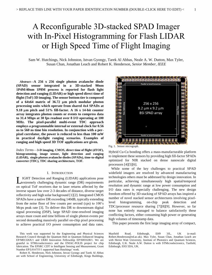
Fig. 1. Sensor micrograph.

> REPLACE THIS LINE WITH YOUR PAPER IDENTIFICATION NUMBER (DOUBLE-CLICK HERE TO EDIT) <
2
reconfigurable SPAD time-resolved pixels in a 3D-stacked
90nm 1P4M/40nm 1P8M CMOS technology. We address pixel
power consumption by employing an in-pixel correlator which
triggers TDC activity only on multiple photon detections within
nanosecond timescales most likely to occur from short laser
pulses rather than background light or dark count [10]. In
addition, power is conserved by a selectable internal/external
TDC clock generation which uses high resolution internal TDC
power sparingly in small time ranges to refine coarse but lower
power range estimates from external TDC clocking. Dynamic
range is tackled by in-pixel integration of photon counts or
events in a counter bank, with TDC throughput enhanced by a
multi-event shift-register approach.
II. SENSOR DESIGN
Fig. 1 shows a chip micrograph indicating the positions of
the main functional blocks. Little circuit detail is visible
because of the backside illuminated silicon of the top tier. Fig.
2 shows the chip organization, 8 I/O pads generate a modest
31.6 Mbps of pixel data at the targeted 30fps (a maximum of
800 Mbps at 760 fps). Pixels are read out by a pairwise rolling
scheme from the center outwards over 256 16-bit column buses.
Two exposure schemes are employed, either rolling pairwise
readout while all other rows are in integration or a global shutter
scheme where all rows are in integration which is then
suspended before readout. A uniform top tier BSI matrix of 256
x 256 pwell/deep-nwell SPADs at 9.18 m pitch with 51% fill-
factor occupies the top tier [2][4]. The SPAD has median dark
count rate of 20 cps at 1.5 V excess bias and peak PDP of 28%
at 615 nm falling to around 5% at 900nm [11]. In the bottom-
tier a 64 x 64 matrix of modular pixel processors at 36.72 m
pitch is integrated in 40nm CMOS technology. A dense custom
layout approach employing area-optimized d-type flip-flops has
been employed to allow ~40 M transistors to be integrated
under the 5.38 mm2 focal plane.
The reconfigurable pixel architecture is shown in Fig. 3. A
16 x 14b ripple counter array and mode multiplexer allow the
sensor to operate in a number of imaging modalities which are
summarized in Table 1 including their key signals, resolutions
and main applications. The counter bank can be re-purposed for
either photon counting or as time bins for in-pixel
histogramming. The full resolution 256x256 of the sensor is
available in single photon counting (SPC) mode with a bit depth
commensurate with common full well depths (and hence SNR)
in conventional pinned photodiode pixels (16384). Photon
counting modes can be combined with windowing or electrical
gating of the SPADs suppress background or provide indirect
time of flight or frequency domain lifetime imaging. This
Fig. 2. Sensor architecture showing pixel layout on bottom tier (left) and SPAD layout on top tier (right).
Fig. 3. Pixel architecture
Table. 1. Sensor operating modes

> REPLACE THIS LINE WITH YOUR PAPER IDENTIFICATION NUMBER (DOUBLE-CLICK HERE TO EDIT) <
3
function also provides an option to operate the pixel in global
shutter exposure (with zero parasitic light sensitivity) while the
default is a high temporal aperture (127/128) rolling shutter
exposure.
A gated ring oscillator (GRO) can be used for either single
shot timestamping of single photons for precise but low
throughput time correlated single photon counting (TCSPC). ).
This mode finds use in scientific imaging or long range LIDAR
where the 38ps time resolution and 143 ns range (tunable to
500ns) are suited to common distances and fluorophores. The
same GRO can be employed as the frequency reference for an
in-pixel histogramming mode for short range time of flight with
high photon timing throughput at a modest I/O rate. Here the
time resolution is coarse (560ps upwards in factors of 2) but
finer depth is recovered by peak centroiding. In microscopy
applications the bin size is still sufficient for common
fluorescence lifetimes (few ns decay time). The same GRO can
be employed as the frequency reference for an in-pixel
histogramming mode for short range time of flight with high
photon timing throughput at a modest I/O rate. The various
modes generally involve a tradeoff of spatial and temporal
resolution where the counters and GRO are shared between all
16 SPADs via an XOR tree. Alternatively dynamic range and
counter depth are traded for spatial resolution by chaining
counters or sharing the timing functions of the multi-event TDC
(METDC) or GRO. A counting correlator can be applied with
a variable threshold to suppress background and save power in
all timing modes. Use of an external clock for multi-event
histogramming or STOP clock in single shot timestamping
offer longer time ranges at lower power consumption than the
in-pixel GRO.
Switching between the various modes can be achieved either
instantaneously where the control signals are available on pads
or within around 320ns where reprogramming of the serial
interface is required. Rapidly alternating between say multi-
event histogramming for 3D imaging and SPC mode has been
proven very useful to combine the lower spatial resolution
depth estimation with improved spatial intensity information
[12]. All operating modes apply globally to the whole array and
cannot be reprogrammed on a per-pixel basis.
In SPC mode, the 16 SPADs can be multiplexed directly to a
bank of 16 14-bit counters realizing shot noise limited digital
photon counting imaging with a 16384 photon full-well
capacity (84dB DR). GS-HDR modes are realised by chaining
the counters into 8 x 28b whilst binning groups of 4 SPADs
allowing 256M photons per SPAD to be counted in an exposure
period with a 64 x 256 spatial resolution. Binning SPADs in
groups of 4 (rather than 2 for higher spatial resolution) was
chosen to allow a ping-pong global-shutter indirect time of
flight mode. This is of value to allow the imager to operate over
long exposure times (1s) without the possibility of counter
saturation even at the peak SPAD event rate of 200 Mcps. The
same 16 counters are repurposed for LIDAR or 3D imaging as
histogram bins for direct time of flight operation where the
resolution is now 64x64 pixels. In this case a tradeoff is made
between temporal and spatial resolution to allow on-chip
integration of timed photons, greatly reduced I/O rates and
extended dynamic range,
Fig. 4 shows the SPAD interface circuit which has been
designed to be highly area-efficient and multi-functional. Only
four thick oxide devices are employed to perform passive
quenching or gating of the SPAD as well as level shifting from
the excess bias voltage Veb (up to 3.3V) to the logic voltage Vdd
of 1.1V. The interface is also agnostic to the SPAD polarity for
compatibility to future top tier detector generations which may
integrate n-on-p or p-on-n SPAD structures. The combination
of external global Vqp and Vqn voltages and the Invert signal
allow selection of either NMOS or PMOS quench transistors
and time gating. An enable SRAM allows masking of noisy
detectors. Two 16-bit datapaths (Fig. 3) connect the SPAD
interface circuits to the pixel counter array, implementing
parallel photon counting or timing using the SPAD(k) or
Start(k) signals respectively. The Start(k) signals act as a start
trigger for the in-pixel TDC which can operate in either single
shot timestamping mode or multi-event histogramming mode.
When ToggleEn is low, only the first photon within a frame
exposure time will be time-stamped by the single shot TDC.
This first photon in the kth SPAD is encoded as a rising edge of
Start(k) and combined by the XOR tree and correlator as
PhotonEdges to initiate single shot timestamping operation
(Fig. 5). Alternatively if the SPAD(k) outputs are used in
conjunction with SPCmode=0, the counters can be used to
count STOP edges to provide per-SPAD photon arrival macro-
times. A macro-time is the coarse time offset from the start of
frame exposure to detection of the first photon arrival, as a
count of the number of laser cycles (or STOP clock cycles). A
macro time can be combined with a micro-time (the fine TDC
timestamp of the photon arrival) to generate a precise time
arrival estimate of the first photon in a frame for every pixel.
When ToggleEn is high, multiple photons can now be time
converted per laser cycle by the multi-event TDC and integrated
in the histogram memory over many laser cycles. Photon
arrivals are encoded on both rising and falling edges of Start(k).
The 16 Start(k) toggling outputs are then mixed via an XOR
tree and correlator to a single sequence PhotonEdges which is
passed to the multi-event TDC (METDC) (Fig. 5).
PhotonEdges is processed by a counter-based correlator
circuit (Fig. 5) which continually counts photons from the first
rising edge received in each a laser cycle. A threshold of 1, 2,
4, 8 photons occurring within a 0.5-10ns delay time (adjustable
Fig. 4. SPAD interfaces
> REPLACE THIS LINE WITH YOUR PAPER IDENTIFICATION NUMBER (DOUBLE-CLICK HERE TO EDIT) <
4
by current starving voltage Vndelay) will generate an output
trigger to start the gated ring oscillator (GRO). This circuit
saves power by only activating the GRO if there is a highly
correlated burst of photons likely to belong to a laser return
while suppressing uncorrelated background light. An example
of the timing of this circuit is shown in Fig. 6. When Qtrig is
asserted, it enables a qualified trigger as the delayed first photon
in the burst provided that the threshold has been met. Although
this creates a histogram with a time-offset, the matching of the
Vndelay controlled current starving circuit is sufficient to allow
acceptable uniformity and simple offset correction. The
toggling trigger sequence can also be generated on multiple
bursts for use in the METDC.
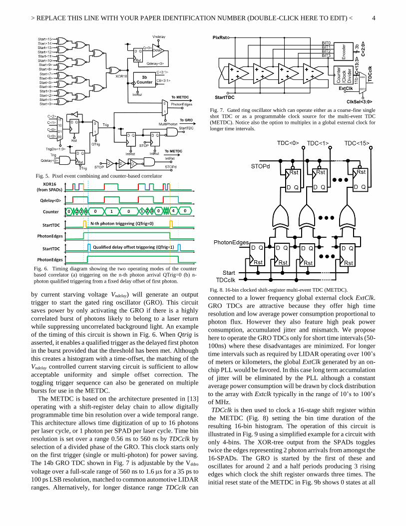
The METDC is based on the architecture presented in [13]
operating with a shift-register delay chain to allow digitally
programmable time bin resolution over a wide temporal range.
This architecture allows time digitization of up to 16 photons
per laser cycle, or 1 photon per SPAD per laser cycle. Time bin
resolution is set over a range 0.56 ns to 560 ns by TDCclk by
selection of a divided phase of the GRO. This clock starts only
on the first trigger (single or multi-photon) for power saving.
The 14b GRO TDC shown in Fig. 7 is adjustable by the Vddro
voltage over a full-scale range of 560 ns to 1.6 s for a 35 ps to
100 ps LSB resolution, matched to common automotive LIDAR
ranges. Alternatively, for longer distance range TDCclk can
connected to a lower frequency global external clock ExtClk.
GRO TDCs are attractive because they offer high time
resolution and low average power consumption proportional to
photon flux. However they also feature high peak power
consumption, accumulated jitter and mismatch. We propose
here to operate the GRO TDCs only for short time intervals (50-
100ns) where these disadvantages are minimized. For longer
time intervals such as required by LIDAR operating over 100’s
of meters or kilometers, the global ExtClk generated by an on-
chip PLL would be favored. In this case long term accumulation
of jitter will be eliminated by the PLL although a constant
average power consumption will be drawn by clock distribution
to the array with Extclk typically in the range of 10’s to 100’s
of MHz.
TDCclk is then used to clock a 16-stage shift register within
the METDC (Fig. 8) setting the bin time duration of the
resulting 16-bin histogram. The operation of this circuit is
illustrated in Fig. 9 using a simplified example for a circuit with
only 4-bins. The XOR-tree output from the SPADs toggles
twice the edges representing 2 photon arrivals from amongst the
16-SPADs. The GRO is started by the first of these and
oscillates for around 2 and a half periods producing 3 rising
edges which clock the shift register onwards three times. The
initial reset state of the METDC in Fig. 9b shows 0 states at all
Fig. 5. Pixel event combining and counter-based correlator
Fig. 6. Timing diagram showing the two operating modes of the counter
based correlator (a) triggering on the n-th photon arrival QTrig=0 (b) n-
photon qualified triggering from a fixed delay offset of first photon.
Fig. 7. Gated ring oscillator which can operate either as a coarse-fine single
shot TDC or as a programmable clock source for the multi-event TDC
(METDC). Notice also the option to multiplex in a global external clock for
longer time intervals.
Fig. 8. 16-bin clocked shift-register multi-event TDC (METDC).

> REPLACE THIS LINE WITH YOUR PAPER IDENTIFICATION NUMBER (DOUBLE-CLICK HERE TO EDIT) <
5
internal nodes. After the first TDCclk edge the high state of
XOR16 is latched into the first position in the shift register (Fig.
9c). On the second TDCclk edge this 1 moves one position
forward and another 1 is introduced as no new photon has
arrived (Fig, 9d). On the third clock edge the XOR16 has
toggled from the second photon and a 0 is introduced (Fig. 9e).
The chain of XORs pick out these transitions in the shift register
generating a multiple hot code. The positions of ones in this
code represent the time offset in TDCclk cycles of photon
arrivals from the STOPd clock which is synchronized to the
pulsed light source. On the high transition of the STOPd clock
this multiple hot code is latched as TDC<3:0> which is
multiplexed into the clock inputs of an array of counters
forming a 4-bin histogram. The bits TDC<0> and TDC<2>
which transition high increment their respective histogram bins
in parallel. Thus multiple photons can be recorded within one
laser cycle compared to a more conventional TDC which places
a single timestamp in a histogram memory per laser cycle.
Readout of the 16 x 14-b counter array is accomplished in
either a rolling shutter or global shutter approach. The pixel
reads out over 4 x 16-bit parallel buses which is subsequently
serialized over 8 I/O pads operating at 100 MHz. Operating at
30 fps the sensor produces a very modest 31.4 Mbps of data
which is readily processed to extract histogram peak locations
by an external FPGA. A frame rate of 760fps has been achieved
in global shutter mode although a glitch in the token-passing
shift register currently limits the sensor to access only half the
available image resolution.
III. SENSOR CHARACTERIZATION
Fig. 10a-d shows a series of 33ms exposure global shutter
photon counting images taken using a white LED array lamp to
illustrate the high dynamic range of the sensor. In 1klux
lighting the 14b counters do not saturate (Fig. 10a). The light
level is increased to 100klux showing saturation and clipping in
the Nikon reference image (Fig. 10b). In the same illumination
conditions the 14b counters rollover and corrupt the image in
the top left corner (Fig. 10c). Detail in this area is recovered in
the tone-mapped 28b photon counting image albeit at four times
lower image resolution (Fig. 10d). No electronic masking or
image post-processing has been applied to remove high DCR
pixels in Fig. 10.
The HDR global shutter mode is insensitive to parasitic light
as the frame is stored in digital form. A DR of 120 dB is seen
in the photon transfer curve in Fig. 11 with peak count rates of
Fig. 9. Simplified timing example of multi-event histogramming operation with
a 4-bin TDC, three clock cycles and two photon arrivals (a) timing diagram (b)
initial state (c) after first clock edge (d) after second clock edge (e) after third
clock edge and rising edge of STOPd.
Fig. 10. SPC mode: (a) 1klux illumination 14b image; (b) side-illuminated
100klux scene with Nikon camera; (c) 100klux illumination 14b code roll-over
image; (d) 100klux illumination 28b image with 4× pixel binning

> REPLACE THIS LINE WITH YOUR PAPER IDENTIFICATION NUMBER (DOUBLE-CLICK HERE TO EDIT) <
6
200 Mcps/SPAD or 13 Tcps for the whole array. We believe
this is the first time the full native SPAD dynamic range is
available in a video rate widefield image sensor.
Fig, 12 shows an impulse response function (IRF) in single
shot TDC mode captured using a 775 nm Coherent Chameleon
Ultra laser operating at 80 MHz. The TDC resolution is 38ps
and the mean FWHM across the array including laser, SPAD
and system jitter is 277 ps with a standard deviation of 30 ps.
Fig. 13 shows the linearity of the single shot TDC operating
in direct ToF as +/-10 cm over a 50 m range. These latter data
were obtained with a 671 nm Picoquant pulsed laser coupled
into a 100 m multimode fiber and passed through a 15 mm
lens to flood illuminate the scene. The pulse duration of the
laser was ~100 ps, the repetition rate was 1.9 MHz, and after
the fibre and imaging lens, the laser power was measured to be
1.8 mW.
Fig. 14 shows distance accuracy in multi-event
histogramming mode improved over that expected from the 560
ps bin size by spreading the pulse energy over bins and
performing centroiding around the peak. As the linearity of the
METDC depends primarily on clock intervals and not delay cell
matching, the INL and DNL are far in excess of the 4-b level.
Fig. 15 shows a map of INL/DNL across the array taken by
uniformly illuminating the image with uncorrelated light and
performing a code density test. The linearity in this mode
exceeds the few bits expected from the 16bins as the bin spacing
is only dependent on clock edges within the shift register.
Fig. 16 shows the operation of the in-pixel counter based
correlator with a threshold of 2 (a logic error prevents
characterization of 4 and 8 thresholds). A 3.5 ns laser pulse is
generated by an 840nm Picoquant Laser Diode at 3.8 MHz. A
controlled background light level is generated by a blue 450 nm
LED operated with 20 mA bias current causing the SPAD to
operate around 900 kcps (measured in SPC mode). The TDC
histograms are shown in single-shot timestamping mode with
laser on in all cases for a single pixel with combinations of
Fig. 11 Photon transfer curve in HDR mode
200Mcps/SPAD
13Tcps for 256x256 array
Fig. 12. Impulse response function in single shot TDC mode (170ps FWHM)
Fig. 13. Linearity in single shot TDC mode
Fig. 14. Linearity in multi-event histogramming mode
Fig. 15. Linearity in histogramming TDC mode
> REPLACE THIS LINE WITH YOUR PAPER IDENTIFICATION NUMBER (DOUBLE-CLICK HERE TO EDIT) <
7
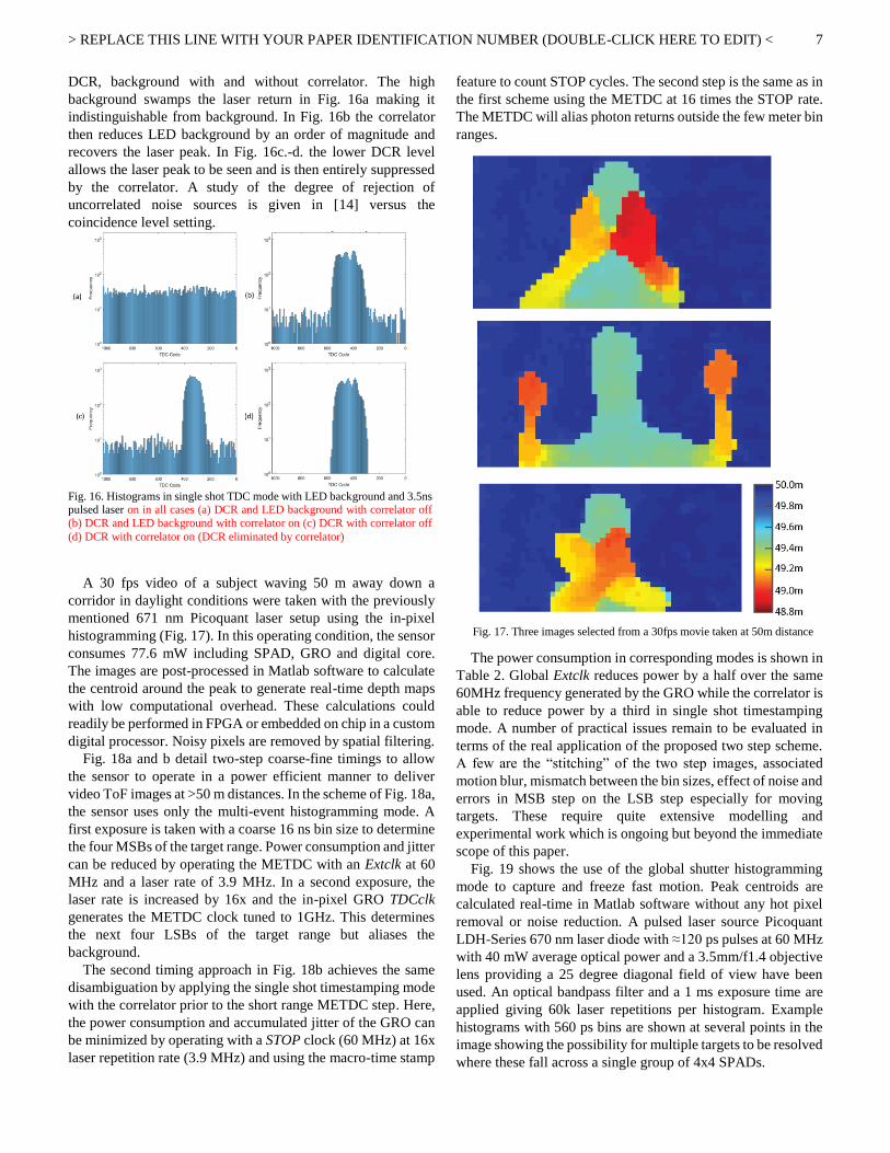
DCR, background with and without correlator. The high
background swamps the laser return in Fig. 16a making it
indistinguishable from background. In Fig. 16b the correlator
then reduces LED background by an order of magnitude and
recovers the laser peak. In Fig. 16c.-d. the lower DCR level
allows the laser peak to be seen and is then entirely suppressed
by the correlator. A study of the degree of rejection of
uncorrelated noise sources is given in [14] versus the
coincidence level setting.
A 30 fps video of a subject waving 50 m away down a
corridor in daylight conditions were taken with the previously
mentioned 671 nm Picoquant laser setup using the in-pixel
histogramming (Fig. 17). In this operating condition, the sensor
consumes 77.6 mW including SPAD, GRO and digital core.
The images are post-processed in Matlab software to calculate
the centroid around the peak to generate real-time depth maps
with low computational overhead. These calculations could
readily be performed in FPGA or embedded on chip in a custom
digital processor. Noisy pixels are removed by spatial filtering.
Fig. 18a and b detail two-step coarse-fine timings to allow
the sensor to operate in a power efficient manner to deliver
video ToF images at >50 m distances. In the scheme of Fig. 18a,
the sensor uses only the multi-event histogramming mode. A
first exposure is taken with a coarse 16 ns bin size to determine
the four MSBs of the target range. Power consumption and jitter
can be reduced by operating the METDC with an Extclk at 60
MHz and a laser rate of 3.9 MHz. In a second exposure, the
laser rate is increased by 16x and the in-pixel GRO TDCclk
generates the METDC clock tuned to 1GHz. This determines
the next four LSBs of the target range but aliases the
background.
The second timing approach in Fig. 18b achieves the same
disambiguation by applying the single shot timestamping mode
with the correlator prior to the short range METDC step. Here,
the power consumption and accumulated jitter of the GRO can
be minimized by operating with a STOP clock (60 MHz) at 16x
laser repetition rate (3.9 MHz) and using the macro-time stamp
feature to count STOP cycles. The second step is the same as in
the first scheme using the METDC at 16 times the STOP rate.
The METDC will alias photon returns outside the few meter bin
ranges.
The power consumption in corresponding modes is shown in
Table 2. Global Extclk reduces power by a half over the same
60MHz frequency generated by the GRO while the correlator is
able to reduce power by a third in single shot timestamping
mode. A number of practical issues remain to be evaluated in
terms of the real application of the proposed two step scheme.
A few are the “stitching” of the two step images, associated
motion blur, mismatch between the bin sizes, effect of noise and
errors in MSB step on the LSB step especially for moving
targets. These require quite extensive modelling and
experimental work which is ongoing but beyond the immediate
scope of this paper.
Fig. 19 shows the use of the global shutter histogramming
mode to capture and freeze fast motion. Peak centroids are
calculated real-time in Matlab software without any hot pixel
removal or noise reduction. A pulsed laser source Picoquant
LDH-Series 670 nm laser diode with ≈120 ps pulses at 60 MHz
with 40 mW average optical power and a 3.5mm/f1.4 objective
lens providing a 25 degree diagonal field of view have been
used. An optical bandpass filter and a 1 ms exposure time are
applied giving 60k laser repetitions per histogram. Example
histograms with 560 ps bins are shown at several points in the
image showing the possibility for multiple targets to be resolved
where these fall across a single group of 4x4 SPADs.
Fig. 16. Histograms in single shot TDC mode with LED background and 3.5ns pulsed laser on in all cases (a) DCR and LED background with correlator off
(b) DCR and LED background with correlator on (c) DCR with correlator off
(d) DCR with correlator on (DCR eliminated by correlator)
Fig. 17. Three images selected from a 30fps movie taken at 50m distance

> REPLACE THIS LINE WITH YOUR PAPER IDENTIFICATION NUMBER (DOUBLE-CLICK HERE TO EDIT) <
8
Table 3 compares this sensor with other recent advanced
SPAD sensors. Our sensor is distinguished by low power
consumption, high sensitivity and small pixel pitch as well as
multi-mode imaging capability at a high dynamic range.
(a)
(b)
Fig. 18. Two proposed schemes to disambiguate short range (2m)
histogramming over typical automotive (50m) LIDAR ranges.
Table 2. Power consumption in the modes proposed in Fig. 18.
Histogram TDC Mode Single Shot TDC Mode
Scenario GRO
clock
(60MHz)
Extclk
(60MHz)
GRO
clock
(1 GHz)
DCR + No
corr.
DCR +
Corr +
Laser
Bckgnd
+ Laser
No Corr.
Bckgnd
+ Laser
Corr.
VHV Power (mW) 36 36 36 0.13 0.18 0.88 0.9
Vddro Power (mW) 66 0.8 6.8 0.67 0.64 0.61 0.64
Vdd Power (mW) 98.6 41.8 125 60.8 32.8 100.6 32.8
(a) (b) (c)
(d)
(e)
(f)
Fig. 19. Three consecutive ToF frames of a 1000 RPM fan taken at 380fps and
1ms exposure. Panel e shows distinct histogram peaks for both the fan blade
edge and the backdrop, with adjacent points shown in panels e and f.
Table 3. Comparison with the state of the art in SPAD sensors
Parameters Units This Work [8] [9] [10] [2]
Sensor
CMOS Technology - 90nm 1P4M/
40nm 1P8M
180nm 45nm/65nm 150nm 180nm
Pixel Array - 256x256/64x64 252x144 16x8 64x64 16x1/32x1
Pixel Pitch m 9.18/36.72 28.5 19.8 60 21
Fill-factor % 51 28 31.3/50.6 26.5 70
Median
DCR@Veb
cps [email protected] 195 @5V [email protected] 6.8k@3V 2.65k@NA
TDC depth bits 14/4 12 14 16/15 12
TDC resolution ps 35/560 48.8 60-320 250-20000 208
TDC area m2 130/150 4200 550 NA NA
TDC number - 4096 1728 1 4096 64
TDC linearity
DNL/INL
LSB +0.05/-0.05
+0.1/-0.08
+0.6/-0.48
+0.89/-1.67
+0.8/-0.7
+3.4/-0.8
+1.2/-1
+4.8/-3.2
+0.15/-0.17
+0.32/-0.56
LIDAR Measurement
Image resolution - 64x64 252x144 256x256 64x64 202x96
Laser projection - Flash Flash Scanning Flash Scanning
Wavelength nm 671 637 532 470 870
Repetition rate MHz 1.9 40 1 NA 0.133
Mean illumination
power
mW 1.8 2 6 NA 21
PDP@ illumination
wavelength@Veb
% 23@3V 33.7@5V [email protected] 20@3V NA
Max distance m 50 50 150-430 367-5862 128
Imaging range m 50 0.7 4.5 NA 100
FOV deg. 1.2x1.2 40x20 NA NA
Accuracy m(%) 0.17(0.34) 0.088(0.17) 0.07(0.3) 1.5(0.37) 11(0.11)
Background light - 1 klux dark NA 100M/pix/s 70 klux
Target reflectivity - white white white NA 9%
Power
consumption
mW 77.6 2540 NA 93.5 530

> REPLACE THIS LINE WITH YOUR PAPER IDENTIFICATION NUMBER (DOUBLE-CLICK HERE TO EDIT) <
9
IV. CONCLUSION
It has been demonstrated that a compact SPAD pixel can be
designed in advanced stacked-3D manufacturing technologies
offering reconfigurable functionalities to reduce power and
extend dynamic range enabling fast 3D imaging and flash
LIDAR applications. Tradeoffs are made in the spatial and
temporal resolution as well as sharing of resources amongst
SPADs to achieve practical performance levels.
REFERENCES
[1] R. Halterman and M. Bruch, “Velodyne HDL-64E lidar for unmanned
surface vehicle obstacle detection,” Proc. SPIE, Unmanned Syst. Technol. XII,
vol. 7692, p. 76920D, May 2010, [2] C. Niclass et al., "A 100-m Range 10-Frame/s 340 x 96-Pixel Time-of-Flight
Depth Sensor in 0.18 m CMOS," in IEEE JSSC, 2013.
[3] A. Eisele and R. Henderson, “185 MHz count rate, 139 dB dynamic range single-photon avalanche diode with active quenching circuit in 130nm CMOS
technology,” in Proc. Int. Image Sensor Workshop, 2011, pp. 6–8.
[4] T. A. Abbas et al., "Backside illuminated SPAD image sensor with 7.83μm pitch in 3D-stacked CMOS technology," IEDM 2016.
[5] S. Lhostis, A. Farcy, E. Deloffre, F. Lorut, S. Mermoz, Y. Henrion, L.
Berthier, F. Bailly, D. Scevola, F. Guyader, F. Gigon, C. Besset, S. Pellissier, L. Gay, N. Hotellier, A. -L. Le Berrigo, S. Moreau, V. Balan, F. Fournel, A.
Jouve, S. Ch´eramy, M. Arnoux, B. Rebhan, G. A. Maier and L. Chitu,
”Reliable 300 mm Wafer Level Hybrid Bonding for 3D Stacked CMOS Image Sensors,” 2016 IEEE 66th Electronic Components and Technology Conference
(ECTC), Las Vegas, NV, 2016, pp. 869-876.
[6] S. Lindner, S. Pellegrini, Y. Henrion, B. Rae, M. Wolf, and E. Charbon, “A high-PDE, backside-illuminated SPAD in 65/40-nm 3D IC CMOS pixel with
cascoded passive quenching and active recharge,” IEEE Electron Device Lett.,
vol. 38, no. 11, pp. 1547–1550, Nov. 2017. [7] M.-J. Lee and E. Charbon, “Progress in single-photon avalanche diode
image sensors in standard CMOS: From two-dimensional monolithic to three-
dimensional-stacked technology”, Japanese Journal of Applied Physics 57, 1002A3 (2018)
[8] Zhang et al., “A 30-frames/s, 252 × 144 SPAD Flash LiDAR With 1728
Dual-Clock 48.8-ps TDCs, and Pixel-Wise Integrated Histogramming”, IEEE J. Solid-State Circuits, Vol. 54, No. 4, pp. 1137-1151, April 2019
[9] A. Ximenes et al., “A 256×256 45/65nm 3D-stacked SPAD-based direct
TOF image sensor for LiDAR applications with optical polar modulation for up to 18.6dB interference suppression”, ISSCC 2018.
[10] M. Perenzoni et al., "A 64 x 64-Pixels Digital Silicon Photomultiplier
Direct TOF Sensor With 100-MPhotons/s/pixel Background Rejection and Imaging/Altimeter Mode With 0.14% Precision Up To 6 km for Spacecraft
Navigation and Landing," in IEEE JSSC, 2017.
[11] T. Al Abbas, D. Chitnis, F. Mattioli Della Rocca, R. K. Henderson, “Dual Layer 3D-Stacked High Dynamic Range SPAD Pixel”, in Proceedings of IISW
(IISS, 2019), pp. 206–209.
[12] I. Gyongy, S. W. Hutchings, M. Tyler, S. Chan, F. Zhu, R. K. Henderson, J. Leach, “1kFPS Time-of-Flight Imagng with a 3D-stacked CMOS SPAD
Sensor”, in Proceedings of IISW (IISS, 2019), pp. 226–229.
[13] N. A. W. Dutton et al., "11.5 A time-correlated single-photon-counting sensor with 14GS/S histogramming time-to-digital converter," ISSCC 2015.
[14] M. Beer et al. “Background Light Rejection in SPAD-Based LiDAR
Sensors by Adaptive Photon Coincidence Detection.” Sensors (Basel, Switzerland) vol. 18,12 4338. 8 Dec. 2018.
Author biographies will be available at time of publication.