a plug and play interface using xilinx fpgasweb.engr.oregonstate.edu/~sllu/fpga/plugplay.pdfa plug...
TRANSCRIPT
®
May, 1995 Application Note BY BILL ALLAIRE AND STEVE KNAPP
© 1995 Xilinx, Inc. All rights reserved. PRELIMINARY—SUBJECT TO CHANGE Version 0.90
A Plug and Play InterfaceUsing Xilinx FPGAs
Summary
This Application Note describes a Plug and Play ISA interface reference design using a Xilinx XC4003-6PQ100C, orlarger, FPGA device. This design implements the features used in a majority of Plug and Play designs but does notimplement every option available within the Plug and Play specification.
Table of ContentsAssumptions...............................................................1
Overview ................................................................ .....1
The Xilinx Solution .....................................................1
Plug and Play Card Configuration Sequence ...........2
Plug and Play Auto-configuration Ports ...................3
Sending and Verifying the Initiation Key ..................4
Isolation Protocol .......................................................4
Programming Plug and Play Devices ........................6
Plug and Play Register Summary ..............................7
Control Register Space ..............................................7
Plug and Play Isolation Sequence.............................9
Reading Resource Data..............................................9
Configuring Card Resource Usage............................9
Resource Programming ...........................................10
Run Time Access to Plug and Play registers..........10
High-Volume, Cost-Reduction Strategies ...............10
Using the Xilinx Plug and Play Design Files...........11
Additional Resources ...............................................12
Assumptions
This application note assumes that the reader has:
n A copy of the Plug and Play ISA Specification.
n A basic understanding of the Plug and Play ISAfunctionality.
n An understanding of the ISA bus functionality.
n A working knowledge of the Xilinx XACT develop-ment system.
The “Additional Resources” section describes where tofind additional information on these topics.
Overview
The ISA bus is the most popular expansion standard inthe PC industry. Unfortunately, ISA has no definedhardware or software mechanism for allocating re-sources among the various ISA cards in a system.Consequently, users typically configure ISA cards using
“jumpers” that change the decode maps for memory andI/O space and steer the DMA and interrupt signals todifferent pins on the bus. Usually, system configurationfiles need to be updated to reflect these changes. Userstypically resolve any sharing conflicts between boards inthe system by referring to the documentation providedby each card manufacturer. For most users, this con-figuration process can be frustrating, time-consuming,and error-prone.
Other common PC bus standards—like Micro Channel,EISA, and PCI—have hardware and software mecha-nisms to automatically identify the resources requestedby a card and to resolve conflicts. Unfortunately, theseexisting mechanisms are not compatible with the hugeinstalled base of PCs with ISA card slots.
The Plug and Play ISA specification provides a hard-ware and software mechanism to resolve resource con-flicts between various Plug and Play-compatible ISAcards in a system. The Plug and Play software opti-mally allocates system resources between the Plug andPlay ISA cards and other devices in the system withoutuser intervention.
A system that uses only Plug Play ISA cards shouldautomatically configure. However, Plug and Play ISAcards will usually co-exist with current generation ISAcards in the same system. In such cases, user interac-tion may still be necessary, although the configuration isaugmented in the BIOS and/or operating system tomanage and arbitrate ISA bus resources.
The Plug and Play ISA specification requires that eachcard support identification, resource usage determina-tion, conflict detection, and conflict resolution. Thespecification also presents a process for software toautomatically configure the new cards without user in-tervention.
The Xilinx Solution
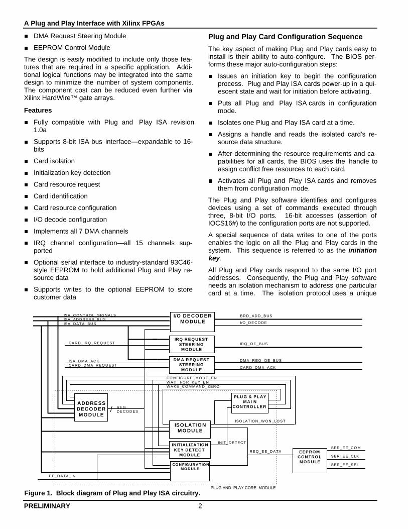
This application note includes all the logic and state ma-chines needed to fully support the Plug and Play ISArevision 1.0a using a single Xilinx XC4003-6PQ100CFPGA device. The design includes five basic modules:
n Plug and Play Core Module
n I/O Decoder Module
n IRQ Steering Module
A Plug and Play Interface with Xilinx FPGAs
PRELIMINARY 2
n DMA Request Steering Module
n EEPROM Control Module
The design is easily modified to include only those fea-tures that are required in a specific application. Addi-tional logical functions may be integrated into the samedesign to minimize the number of system components.The component cost can be reduced even further viaXilinx HardWire™ gate arrays.
Features
n Fully compatible with Plug and Play ISA revision1.0a
n Supports 8-bit ISA bus interface—expandable to 16-bits
n Card isolation
n Initialization key detection
n Card resource request
n Card identification
n Card resource configuration
n I/O decode configuration
n Implements all 7 DMA channels
n IRQ channel configuration—all 15 channels sup-ported
n Optional serial interface to industry-standard 93C46-style EEPROM to hold additional Plug and Play re-source data
n Supports writes to the optional EEPROM to storecustomer data
Plug and Play Card Configuration Sequence
The key aspect of making Plug and Play cards easy toinstall is their ability to auto-configure. The BIOS per-forms these major auto-configuration steps:
n Issues an initiation key to begin the configurationprocess. Plug and Play ISA cards power-up in a qui-escent state and wait for initiation before activating.
n Puts all Plug and Play ISA cards in configurationmode.
n Isolates one Plug and Play ISA card at a time.
n Assigns a handle and reads the isolated card's re-source data structure.
n After determining the resource requirements and ca-pabilities for all cards, the BIOS uses the handle toassign conflict free resources to each card.
n Activates all Plug and Play ISA cards and removesthem from configuration mode.
The Plug and Play software identifies and configuresdevices using a set of commands executed throughthree, 8-bit I/O ports. 16-bit accesses (assertion ofIOCS16#) to the configuration ports are not supported.
A special sequence of data writes to one of the portsenables the logic on all the Plug and Play cards in thesystem. This sequence is referred to as the initiationkey .
All Plug and Play cards respond to the same I/O portaddresses. Consequently, the Plug and Play softwareneeds an isolation mechanism to address one particularcard at a time. The isolation protocol uses a unique
ISA _C ON TR OL _SIGN AL SISA _AD D R ES S_B U SISA _D ATA_ BU S
RE GDE C OD ES/
SER _E E_C O M
SER _E E_C LK
SER _E E_S EL
BR D _AD D _B US
I/O_D E C OD E
DM A _R EQ _OE _BU S
CA R D_ D M A_A CK
EE_D A TA _IN
RE Q_E E_D A TA
IN IT_ D ETEC T
ISO LA TION _ W ON _LO ST
CO N FIGU R E _M OD E_ ENW A IT_ FO R _KE Y_E NW A KE _C OM M AN D _ZER O
IR Q_OE_BU S
ISA _D M A_ AC KCA R D_ D M A_R EQ U EST
CA R D_ IR Q _R EQ UE ST
INITIALIZATIO NKEY DETEC T
MO DULE
CO N FIGU R A TIONMO D U LE
PLU G & P LAYMAI N
CON TRO LLE R
I/O DE CO DERMO DULE
IRQ RE Q UESTSTE ER INGMO DULE
AD DRE SSDEC OD E RMO DULE
DMA R EQ UES TSTE ER INGMO DULE
EEP ROMCON TRO LMO DULE
ISO LATIO NMO DULE
Figure 1. Block diagram of Plug and Play ISA circuitry.PLUG AND PLAY CORE MODULE
3 SUBJECT TO CHANGE
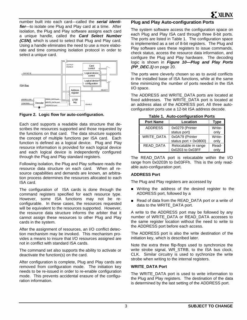
number built into each card—called the serial identi-fier —to isolate one Plug and Play card at a time. Afterisolation, the Plug and Play software assigns each carda unique handle, called the Card Select Number(CSN), which is used to select that Plug and Play card.Using a handle eliminates the need to use a more elabo-rate and time consuming isolation protocol in order toselect a unique card.
Each card supports a readable data structure that de-scribes the resources supported and those requested bythe functions on that card. The data structure supportsthe concept of multiple functions per ISA card. Eachfunction is defined as a logical device. Plug and Playresource information is provided for each logical deviceand each logical device is independently configuredthrough the Plug and Play standard registers.
Following isolation, the Plug and Play software reads theresource data structure on each card. When all re-source capabilities and demands are known, an arbitra-tion process determines the resources allocated to eachISA card.
The configuration of ISA cards is done through thecommand registers specified for each resource type.However, some ISA functions may not be re-configurable. In these cases, the resources requestedwill be equivalent to the resources supported. However,the resource data structure informs the arbiter that itcannot assign these resources to other Plug and Playcards in the system.
After the assignment of resources, an I/O conflict detec-tion mechanism may be invoked. This mechanism pro-vides a means to insure that I/O resources assigned arenot in conflict with standard ISA cards.
The command set also supports the ability to activate ordeactivate the function(s) on the card.
After configuration is complete, Plug and Play cards areremoved from configuration mode. The initiation keyneeds to be re-issued in order to re-enable configurationmode. This prevents accidental erasure of the configu-ration information.
Plug and Play Auto-configuration Ports
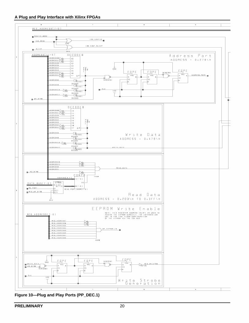
The system software access the configuration space oneach Plug and Play ISA card through three 8-bit ports.The ports are listed in Table 1. The configuration spaceis implemented as a set of 8-bit registers. The Plug andPlay software uses these registers to issue commands,check status, access the resource data information, andconfigure the Plug and Play hardware. The decodinglogic is shown in Figure 10—Plug and Play Ports(PP_DEC.1) on page 20.
The ports were cleverly chosen so as to avoid conflictsin the installed base of ISA functions, while at the sametime minimizing the number of ports needed in the ISAI/O space.
The ADDRESS and WRITE_DATA ports are located atfixed addresses. The WRITE_DATA port is located atan address alias of the ADDRESS port. All three auto-configuration ports use a 12-bit ISA address decode.
Table 1. Auto-configuration PortsPort Name Location Type
ADDRESS 0x0279 (Printerstatus port)
Write-only
WRITE_DATA 0x0A79 (Printerstatus port + 0x0800)
Write-only
READ_DATA Relocatable in range0x0203 to 0x03FF
Read-only
The READ_DATA port is relocatable within the I/Orange from 0x0203h to 0x03FFh. This is the only read-able auto-configuration port.
ADDRESS Port
The Plug and Play registers are accessed by
n Writing the address of the desired register to theADDRESS port, followed by a
n Read of data from the READ_DATA port or a write ofdata to the WRITE_DATA port.
A write to the ADDRESS port may be followed by anynumber of WRITE_DATA or READ_DATA accesses tothe same register location without the need to write tothe ADDRESS port before each access.
The ADDRESS port is also the write destination of theinitiation key, which is described later.
Note the extra three flip-flops used to synchronize thewrite strobe signal, WR_STRB, to the ISA bus clock,CLK. Similar circuitry is used to sychronize the writestrobe when writing to the internal registers.
WRITE_DATA Port
The WRITE_DATA port is used to write information tothe Plug and Play registers. The destination of the datais determined by the last setting of the ADDRESS port.
Logical deviceconfiguration
Logical devicecontrol
Cardcontrol
Addressregister
LFSRkey
ISA Bus
DecoderADDRESS port
WRITE_DATA port
READ_DATA port
ENABLE
SELECT
OUTPUTENABLE
ADDR[11:00]
CONTROL
DATA[7:0]
Figure 2. Logic flow for auto-configuration.
A Plug and Play Interface with Xilinx FPGAs
PRELIMINARY 4
READ_DATA Port
The READ_DATA port is used to read information fromthe Plug and Play registers. The source of the data isdetermined by the last setting of the ADDRESS port.
The address of the READ_DATA port is set by writingthe proper value to a Plug and Play control register.The isolation protocol verifies that the location selectedfor the READ_DATA port is free of conflict.
Sending and Verifying the Initiation Key
The Plug and Play logic is quiescent on power up andmust be enabled by software.
Logic Modules Used
The logic that performs this function is included in thefollowing modules:
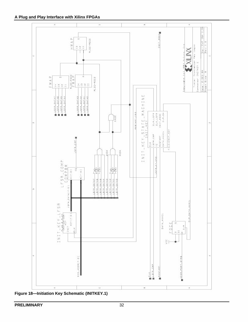
1. the INIT_DETECT symbol shown in Figure 7—Plugand Play Demonstration Design, Sheet 1(PLGPLY.1) on page 14.
2. the underlying logic for INIT_DETECT shown inFigure 18—Initiation Key Schematic (INITKEY.1)on page 32.
3. the ABEL source code for the initiation key statemachine shown in Figure 20—ABEL source filefor Initiation Key state machine (INIT_KEY.ABL)on page 34.
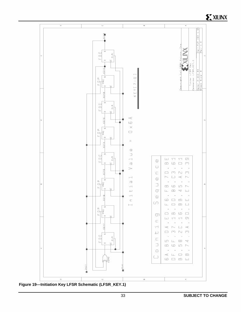
4. the underlying logic for the LFSR initiation keyshown in Figure 19—Initiation Key LFSR Sche-matic (LFSR_KEY.1) on page 33.
5. the MAIN_CONTROL symbol shown in Figure 7—Plug and Play Demonstration Design, Sheet 1(PLGPLY.1) on page 14.
6. the ABEL source for the Plug and Play main control-ler (states ‘wait_init’ and ‘sleep’) shown in Figure17—ABEL source file for Plug and Play mainstate machine on page 30.
The initiation key places the Plug and Play logic intoconfiguration mode. This is done by a predefined seriesof writes to the ADDRESS port. The write sequence isdecoded by the logic and state machine in theINIT_DETECT symbol. If the proper series of I/O writesis detected, then the Plug and Play auto-configurationports are enabled.
The hardware verification of the initiation key is ac-complished using a Linear Feedback Shift Register(LFSR) shown in Figure 19. The LFSR powers-up pre-
loaded with 0x6Ah. Software generates the LFSR se-quence, also shown in Figure 19, and writes it to theADDRESS port as a sequence of 8-bit write cycles. Thehardware compares the byte of write data with the valuein the shift register at each write. Any time the datadoes not match, the hardware resets the LFSR to theinitial value. Software should reset the LFSR to its ini-tial value by a sequence of two write cycles of 0x00 tothe ADDRESS port before the initiation key is sent.
Isolation Protocol
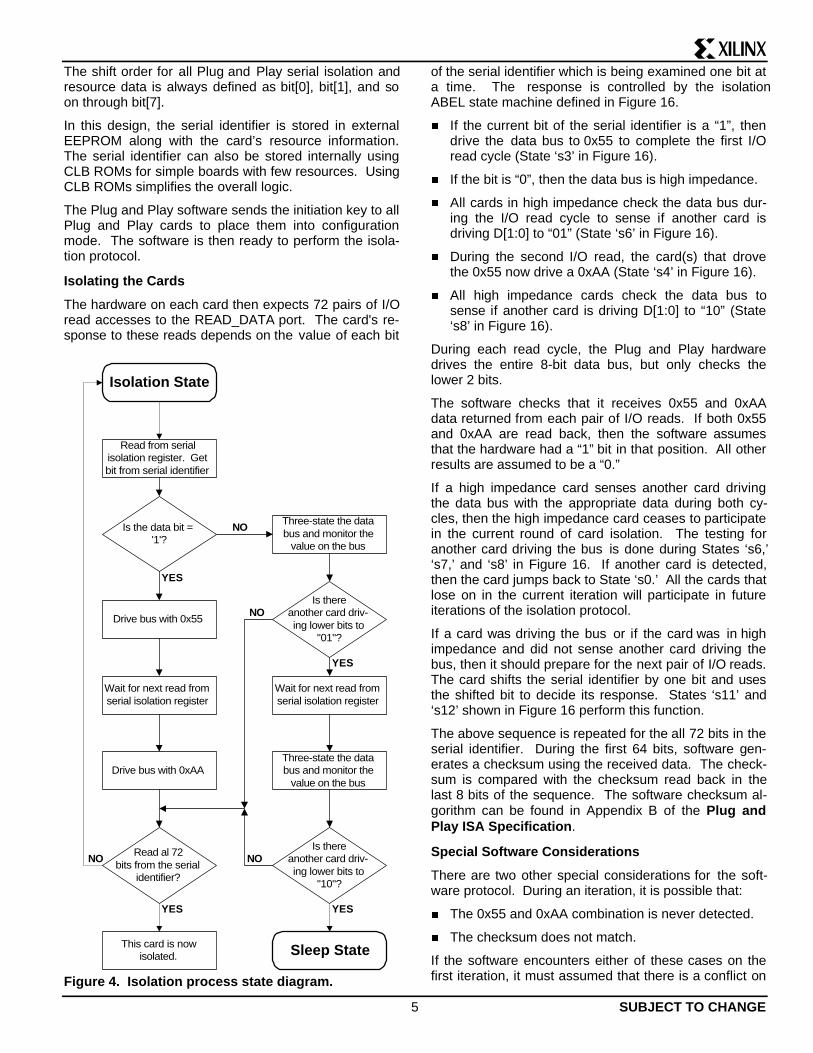
A simple algorithm is used to isolate each Plug and Playcard. This algorithm uses the signals on the ISA busand requires lock-step operation between the Plug andPlay hardware and the isolation software. The statediagram for the isolation process is shown in Figure 4.
Logic Modules Used
The logic that performs the isolation protocol is shown inthe following modules:
1. the ISOLATION symbol shown in Figure 7—Plugand Play Demonstration Design, Sheet 1(PLGPLY.1) on page 14.
2. the underlying logic for ISOLATION shown inFigure 15—Isolation Protocol Schematic(ISO_MOD.1) on page 26.
3. the underlying ABEL source code for the isolationstate machine shown in Figure 16—Isolation StateMachine Listing (ISOLATE.ABL) on page 27.
4. the MAIN_CONTROL symbol shown in Figure 7—Plug and Play Demonstration Design, Sheet 1(PLGPLY.1) on page 14.
5. the ABEL source for the Plug and Play main control-ler shown in Figure 17—ABEL source file for Plugand Play main state machine on page 30.
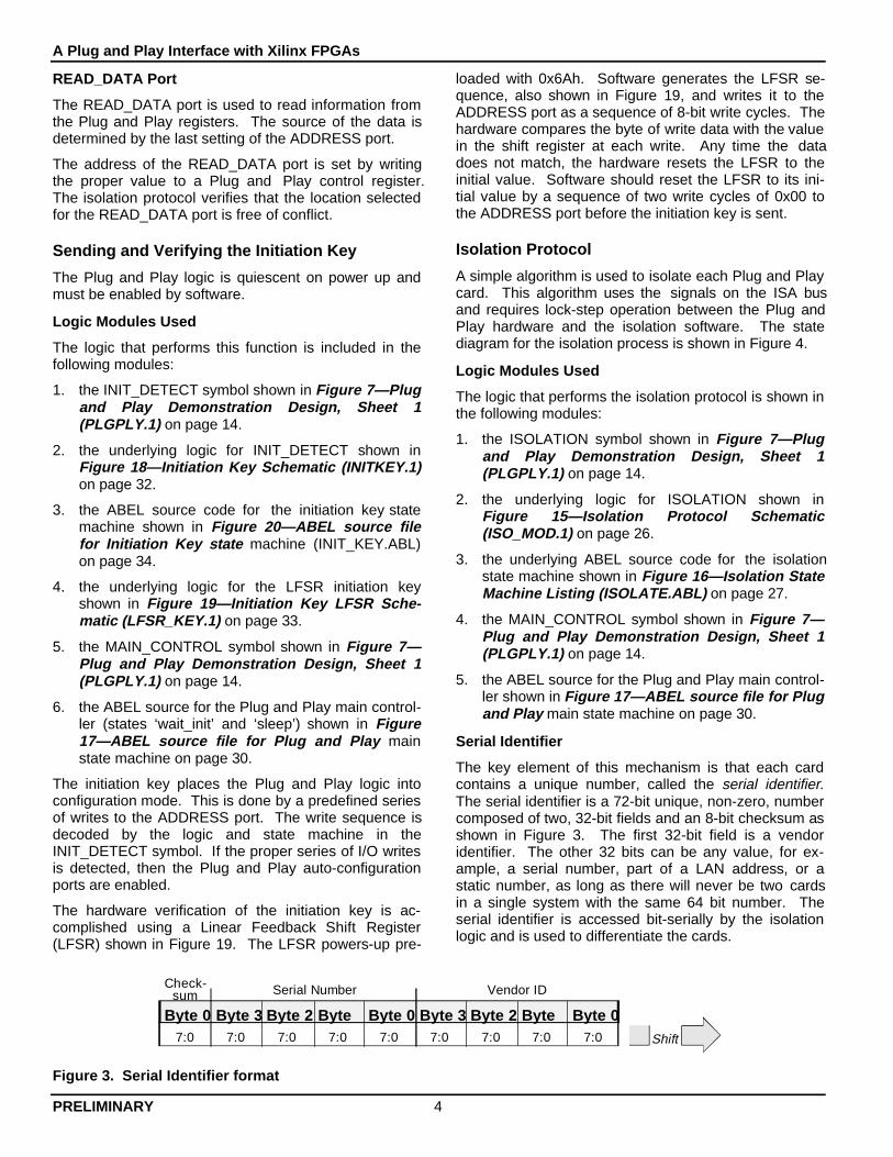
Serial Identifier
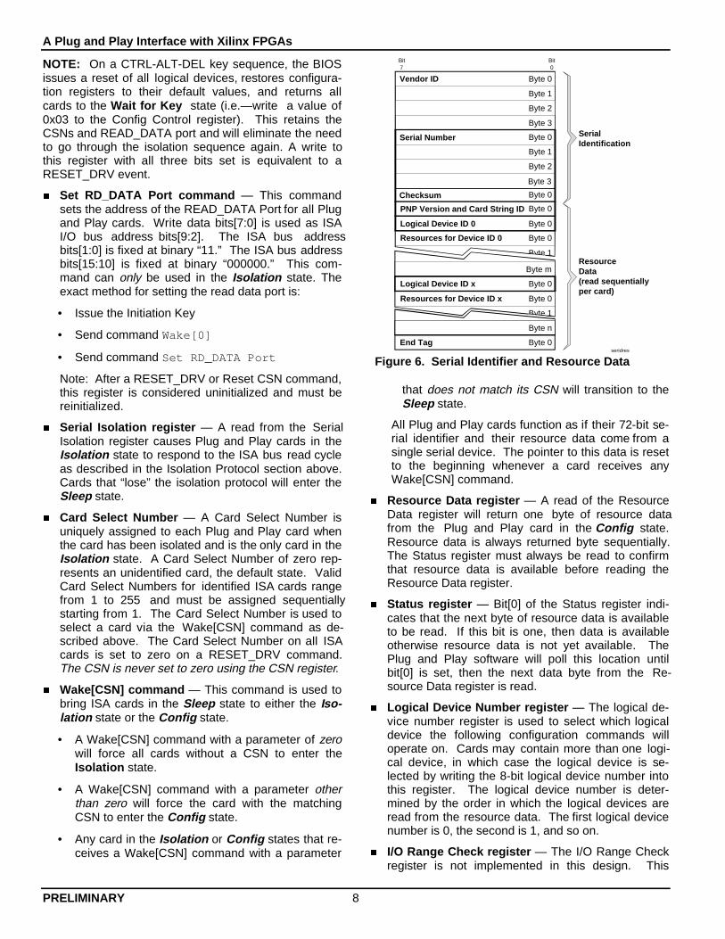
The key element of this mechanism is that each cardcontains a unique number, called the serial identifier.The serial identifier is a 72-bit unique, non-zero, numbercomposed of two, 32-bit fields and an 8-bit checksum asshown in Figure 3. The first 32-bit field is a vendoridentifier. The other 32 bits can be any value, for ex-ample, a serial number, part of a LAN address, or astatic number, as long as there will never be two cardsin a single system with the same 64 bit number. Theserial identifier is accessed bit-serially by the isolationlogic and is used to differentiate the cards.
Byte 0
Vendor ID
7:0
Byte7:0
Byte 27:0
Byte 37:0
Byte 07:0
Byte7:0
Byte 27:0
Byte 37:0
Byte 07:0
Serial NumberCheck-sum
Shift
Figure 3. Serial Identifier format
5 SUBJECT TO CHANGE
The shift order for all Plug and Play serial isolation andresource data is always defined as bit[0], bit[1], and soon through bit[7].
In this design, the serial identifier is stored in externalEEPROM along with the card’s resource information.The serial identifier can also be stored internally usingCLB ROMs for simple boards with few resources. UsingCLB ROMs simplifies the overall logic.
The Plug and Play software sends the initiation key to allPlug and Play cards to place them into configurationmode. The software is then ready to perform the isola-tion protocol.
Isolating the Cards
The hardware on each card then expects 72 pairs of I/Oread accesses to the READ_DATA port. The card's re-sponse to these reads depends on the value of each bit
of the serial identifier which is being examined one bit ata time. The response is controlled by the isolationABEL state machine defined in Figure 16.
n If the current bit of the serial identifier is a “1”, thendrive the data bus to 0x55 to complete the first I/Oread cycle (State ‘s3’ in Figure 16).
n If the bit is “0”, then the data bus is high impedance.
n All cards in high impedance check the data bus dur-ing the I/O read cycle to sense if another card isdriving D[1:0] to “01” (State ‘s6’ in Figure 16).
n During the second I/O read, the card(s) that drovethe 0x55 now drive a 0xAA (State ‘s4’ in Figure 16).
n All high impedance cards check the data bus tosense if another card is driving D[1:0] to “10” (State‘s8’ in Figure 16).
During each read cycle, the Plug and Play hardwaredrives the entire 8-bit data bus, but only checks thelower 2 bits.
The software checks that it receives 0x55 and 0xAAdata returned from each pair of I/O reads. If both 0x55and 0xAA are read back, then the software assumesthat the hardware had a “1” bit in that position. All otherresults are assumed to be a “0.”
If a high impedance card senses another card drivingthe data bus with the appropriate data during both cy-cles, then the high impedance card ceases to participatein the current round of card isolation. The testing foranother card driving the bus is done during States ‘s6,’‘s7,’ and ‘s8’ in Figure 16. If another card is detected,then the card jumps back to State ‘s0.’ All the cards thatlose on in the current iteration will participate in futureiterations of the isolation protocol.
If a card was driving the bus or if the card was in highimpedance and did not sense another card driving thebus, then it should prepare for the next pair of I/O reads.The card shifts the serial identifier by one bit and usesthe shifted bit to decide its response. States ‘s11’ and‘s12’ shown in Figure 16 perform this function.
The above sequence is repeated for the all 72 bits in theserial identifier. During the first 64 bits, software gen-erates a checksum using the received data. The check-sum is compared with the checksum read back in thelast 8 bits of the sequence. The software checksum al-gorithm can be found in Appendix B of the Plug andPlay ISA Specification .
Special Software Considerations
There are two other special considerations for the soft-ware protocol. During an iteration, it is possible that:
n The 0x55 and 0xAA combination is never detected.
n The checksum does not match.
If the software encounters either of these cases on thefirst iteration, it must assumed that there is a conflict on
Isolation State
Read from serialisolation register. Getbit from serial identifier
Is the data bit ='1'?
Three-state the databus and monitor the
value on the bus
Is thereanother card driv-ing lower bits to
"01"?
Wait for next read fromserial isolation register
Wait for next read fromserial isolation register
Drive bus with 0x55
Is thereanother card driv-ing lower bits to
"10"?
Drive bus with 0xAA
Read al 72bits from the serial
identifier?
Sleep StateThis card is nowisolated.
Three-state the databus and monitor the
value on the bus
YES
NO
NO
YES
NO
YESYES
NO
Figure 4. Isolation process state diagram.
A Plug and Play Interface with Xilinx FPGAs
PRELIMINARY 6
the READ_DATA. If a conflict is detected, then theREAD_DATA port needs to be relocated.
The above process is repeated until a non-conflictinglocation for the READ_DATA port is found. The entirerange between 0x200 and 0x3FF is available, howeverin practice it is expected that only a few locations will betried before software determines that no Plug and Playcards are present.
During subsequent iterations, the occurrence of either ofthese two special cases should be interpreted as theabsence of any further Plug and Play cards (i.e.—thelast card was found in the previous iteration). This ter-minates the isolation protocol.
The software must delay 1 msec prior to starting the firstpair of isolation reads, and must wait 250 µsec betweeneach subsequent pair of isolation reads. This delaygives the ISA card time to access information from pos-sibly very slow storage devices.
One Card Remains—The Isolation Winner
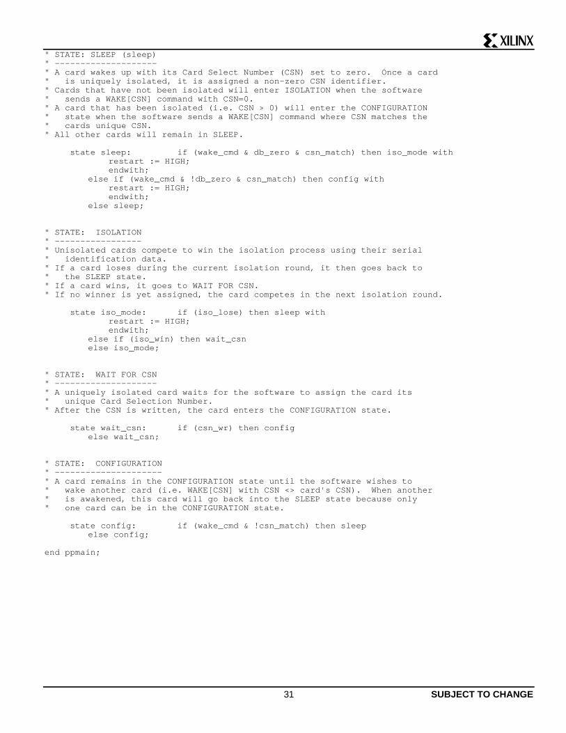
At the end of isolation process, only one card remains.This card is assigned a handle referred to as the CardSelect Number (CSN). The CSN will be used later bythe software to select the card. The logic that controlsthe process is contained in the MAIN_CONTROL sym-bol shown in Figure 7 and in the ABEL state machinelisting showin in Figure 17. The specific states involvedare named ‘iso_mode’ and ‘wait_csn.’
Cards that have already been assigned a CSN do notparticipate in subsequent iterations of the isolation pro-tocol: They have already been uniquely identified. Acards must be assigned a CSN before it will respond toother Plug and Play commands.
The protocol permits the 8-bit checksum to be stored innon-volatile memory on the card or generated by on-card logic in real-time. The same LFSR algorithm de-scribed in the initiation key section is used in the check-sum generation. In this example, the checksum isstored in the EEPROM.
Plug and Play cards must not drive the IOCHRDY signalduring serial isolation. However, cards may driveIOCHRDY at any other time.
Programming Plug and Play Devices
This section describes how configuration resource datais read from Plug and Play ISA cards as well as howresource selections are programmed. The Plug andPlay state machine and Plug and Play commands areintroduced.
The Card Select Number (CSN) register is written duringthe isolation process and is actively involved in mostPlug and Play commands. The CSN is an 8-bit registerused to select one or more ISA cards and is shown asCSN_REGISTER toward the top of Figure 7.
The CSN is an 8-bit register because it allows a widevariety of devices to manage their configuration andcontrol using this mechanism. The CSN is defined suchthat all cards power-up with this register set to zero(0x00). Once a card has been isolated, the CSN on thatcard is assigned a unique, non-zero value. This valueallows the Plug and Play software to select this card atlater points in the configuration process without goingthrough the isolation protocol again.
Logic Modules Used
1. the CSN_REGISTER symbol shown in Figure 7—Plug and Play Demonstration Design, Sheet 1(PLGPLY.1) on page 14.
2. the MAIN_CONTROL symbol shown in Figure 7—Plug and Play Demonstration Design, Sheet 1(PLGPLY.1) on page 14.
3. the ABEL source for the Plug and Play main control-ler shown in Figure 17—ABEL source file for Plugand Play main state machine on page 30.
Main Controller States
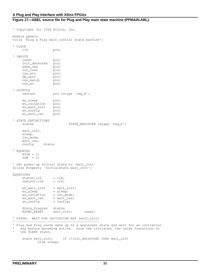
The Plug and Play control states are summarized asfollows:
n Wait for Key — State ‘wait_init’ in Figure 17. Allcards enter this state after initial power-up or in re-sponse to the Wait for Key command. No com-mands are active in this state until the initiation keyis detected on the ISA bus. The Wait for Key stateis the default state for Plug and Play cards duringnormal system operation. After configuration andactivation, software should return all cards to thisstate.
n Sleep — State ‘sleep’ in Figure 17. In this state,Plug and Play cards wait for a Wake[CSN] com-mand. This command selectively enables one ormore cards to enter either the Isolation or Configstates based on the write data and the value of theCSN on each card. Cards leave the Sleep state inresponse to a Wake[CSN] command when the valueof write data bits[7:0] of the command matches thecard’s unique CSN. All the cards that have not beenassigned a CSN value have CSN=0x00 (the defaultvalue). If the write data for the Wake[CSN] com-mand is zero then all cards that have not been as-signed a CSN will enter the Isolation state. If thewrite data for the Wake[CSN] command is not zerothen the one card whose assigned CSN matches theparameter of the Wake[CSN] command will enter theConfig state.
n Isolation — State ‘iso_mode’ in Figure 17. In thisstate, Plug and Play cards respond to reads of theSerial Isolation Register as described in the previoussection on the isolation process. Once a card is iso-lated, it is a assigned unique CSN value in State‘wait_csn’ in Figure 17. This number will later beused by the Wake[CSN] command to select the card.
7 SUBJECT TO CHANGE
Once the CSN is written, the card transitions to theConfig state.
n n Config — State ‘config’ in Figure 17. A card in theConfig state responds to all configuration commandsincluding reading the card's resource configurationinformation and programming the card's resourceselections. Only one card may be in this state at atime.
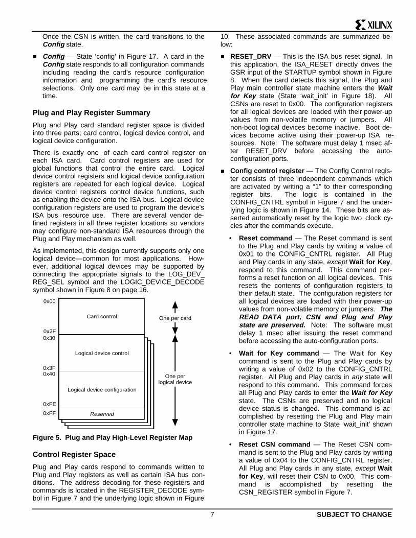
Plug and Play Register Summary
Plug and Play card standard register space is dividedinto three parts; card control, logical device control, andlogical device configuration.
There is exactly one of each card control register oneach ISA card. Card control registers are used forglobal functions that control the entire card. Logicaldevice control registers and logical device configurationregisters are repeated for each logical device. Logicaldevice control registers control device functions, suchas enabling the device onto the ISA bus. Logical deviceconfiguration registers are used to program the device'sISA bus resource use. There are several vendor de-fined registers in all three register locations so vendorsmay configure non-standard ISA resources through thePlug and Play mechanism as well.
As implemented, this design currently supports only onelogical device—common for most applications. How-ever, additional logical devices may be supported byconnecting the appropriate signals to the LOG_DEV_REG_SEL symbol and the LOGIC_DEVICE_DECODEsymbol shown in Figure 8 on page 16.
c
Card control
0x00
0x2F
One perlogical device
One per card
Logical device control
Logical device configuration
Reserved
0x30
0x3F0x40
0xFE
0xFF
Figure 5. Plug and Play High-Level Register Map
Control Register Space
Plug and Play cards respond to commands written toPlug and Play registers as well as certain ISA bus con-ditions. The address decoding for these registers andcommands is located in the REGISTER_DECODE sym-bol in Figure 7 and the underlying logic shown in Figure
10. These associated commands are summarized be-low:
n RESET_DRV — This is the ISA bus reset signal. Inthis application, the ISA_RESET directly drives theGSR input of the STARTUP symbol shown in Figure8. When the card detects this signal, the Plug andPlay main controller state machine enters the Waitfor Key state (State ‘wait_init’ in Figure 18). AllCSNs are reset to 0x00. The configuration registersfor all logical devices are loaded with their power-upvalues from non-volatile memory or jumpers. Allnon-boot logical devices become inactive. Boot de-vices become active using their power-up ISA re-sources. Note: The software must delay 1 msec af-ter RESET_DRV before accessing the auto-configuration ports.
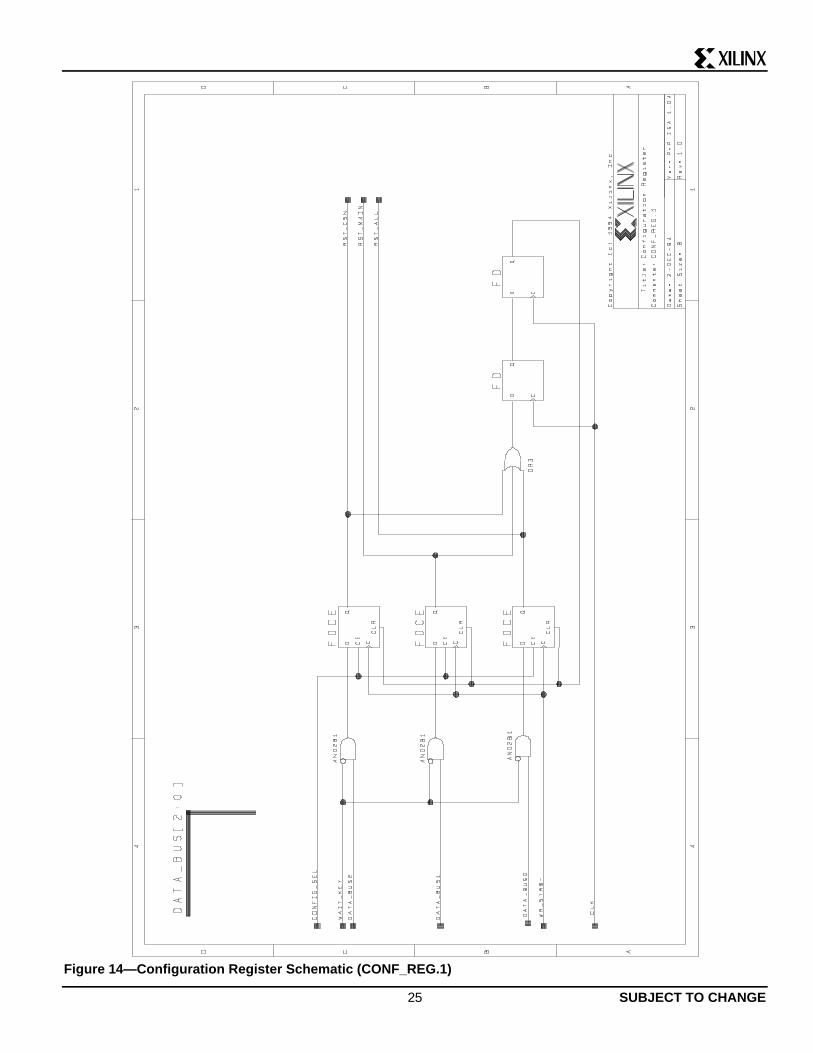
n Config control register — The Config Control regis-ter consists of three independent commands whichare activated by writing a “1” to their correspondingregister bits. The logic is contained in theCONFIG_CNTRL symbol in Figure 7 and the under-lying logic is shown in Figure 14. These bits are as-serted automatically reset by the logic two clock cy-cles after the commands execute.
• Reset command — The Reset command is sentto the Plug and Play cards by writing a value of0x01 to the CONFIG_CNTRL register. All Plugand Play cards in any state, except Wait for Key ,respond to this command. This command per-forms a reset function on all logical devices. Thisresets the contents of configuration registers totheir default state. The configuration registers forall logical devices are loaded with their power-upvalues from non-volatile memory or jumpers. TheREAD_DATA port, CSN and Plug and Playstate are preserved. Note: The software mustdelay 1 msec after issuing the reset commandbefore accessing the auto-configuration ports.
• Wait for Key command — The Wait for Keycommand is sent to the Plug and Play cards bywriting a value of 0x02 to the CONFIG_CNTRLregister. All Plug and Play cards in any state willrespond to this command. This command forcesall Plug and Play cards to enter the Wait for Keystate. The CSNs are preserved and no logicaldevice status is changed. This command is ac-complished by resetting the Plug and Play maincontroller state machine to State ‘wait_init’ shownin Figure 17.
• Reset CSN command — The Reset CSN com-mand is sent to the Plug and Play cards by writinga value of 0x04 to the CONFIG_CNTRL register.All Plug and Play cards in any state, except Waitfor Key , will reset their CSN to 0x00. This com-mand is accomplished by resetting theCSN_REGISTER symbol in Figure 7.
A Plug and Play Interface with Xilinx FPGAs
PRELIMINARY 8
NOTE: On a CTRL-ALT-DEL key sequence, the BIOSissues a reset of all logical devices, restores configura-tion registers to their default values, and returns allcards to the Wait for Key state (i.e.—write a value of0x03 to the Config Control register). This retains theCSNs and READ_DATA port and will eliminate the needto go through the isolation sequence again. A write tothis register with all three bits set is equivalent to aRESET_DRV event.
n Set RD_DATA Port command — This commandsets the address of the READ_DATA Port for all Plugand Play cards. Write data bits[7:0] is used as ISAI/O bus address bits[9:2]. The ISA bus addressbits[1:0] is fixed at binary “11.” The ISA bus addressbits[15:10] is fixed at binary “000000.” This com-mand can only be used in the Isolation state. Theexact method for setting the read data port is:
• Issue the Initiation Key
• Send command Wake[0]
• Send command Set RD_DATA Port
Note: After a RESET_DRV or Reset CSN command,this register is considered uninitialized and must bereinitialized.
n Serial Isolation register — A read from the SerialIsolation register causes Plug and Play cards in theIsolation state to respond to the ISA bus read cycleas described in the Isolation Protocol section above.Cards that “lose” the isolation protocol will enter theSleep state.
n Card Select Number — A Card Select Number isuniquely assigned to each Plug and Play card whenthe card has been isolated and is the only card in theIsolation state. A Card Select Number of zero rep-resents an unidentified card, the default state. ValidCard Select Numbers for identified ISA cards rangefrom 1 to 255 and must be assigned sequentiallystarting from 1. The Card Select Number is used toselect a card via the Wake[CSN] command as de-scribed above. The Card Select Number on all ISAcards is set to zero on a RESET_DRV command.The CSN is never set to zero using the CSN register.
n Wake[CSN] command — This command is used tobring ISA cards in the Sleep state to either the Iso-lation state or the Config state.
• A Wake[CSN] command with a parameter of zerowill force all cards without a CSN to enter theIsolation state.
• A Wake[CSN] command with a parameter otherthan zero will force the card with the matchingCSN to enter the Config state.
• Any card in the Isolation or Config states that re-ceives a Wake[CSN] command with a parameter
that does not match its CSN will transition to theSleep state.
All Plug and Play cards function as if their 72-bit se-rial identifier and their resource data come from asingle serial device. The pointer to this data is resetto the beginning whenever a card receives anyWake[CSN] command.
n Resource Data register — A read of the ResourceData register will return one byte of resource datafrom the Plug and Play card in the Config state.Resource data is always returned byte sequentially.The Status register must always be read to confirmthat resource data is available before reading theResource Data register.
n Status register — Bit[0] of the Status register indi-cates that the next byte of resource data is availableto be read. If this bit is one, then data is availableotherwise resource data is not yet available. ThePlug and Play software will poll this location untilbit[0] is set, then the next data byte from the Re-source Data register is read.
n Logical Device Number register — The logical de-vice number register is used to select which logicaldevice the following configuration commands willoperate on. Cards may contain more than one logi-cal device, in which case the logical device is se-lected by writing the 8-bit logical device number intothis register. The logical device number is deter-mined by the order in which the logical devices areread from the resource data. The first logical devicenumber is 0, the second is 1, and so on.
n I/O Range Check register — The I/O Range Checkregister is not implemented in this design. This
Byte 0PNP Version and Card String ID
Byte 0
End Tag
Byte 0
Byte 0Serial Number
Byte 3
Byte 2
Byte 1
Byte 0Vendor ID
Byte 1
Byte 2
Byte 3
Bit7
Bit0
SerialIdentification
ResourceData(read sequentiallyper card)
seridres
Checksum Byte 0
Logical Device ID 0
Resources for Device ID 0
Byte 1
Byte m
Byte 0
Byte 0Logical Device ID x
Resources for Device ID x
Byte 1
Byte n
Byte 0
Figure 6. Serial Identifier and Resource Data
9 SUBJECT TO CHANGE
command is optional and is not implemented oncards that do not have configurable I/O port ranges.
n n Activate register — The Activate register is aread/write register that is used to activate a logicaldevice. An active logical device responds to all ISAbus cycles as per its normal operation. An inactivelogical device does not respond to nor drive any ISAbus signals. Bit[0] is the active bit, if it is set to “1”then the logical device is active, otherwise it is inac-tive.
Plug and Play Isolation Sequence
On power up, all Plug and Play cards detectRESET_DRV, set their CSN to 0, and enter the Wait forKey state. There is a required 1 msec delay from eithera RESET_DRV or ResetCmd to any Plug and Play portaccess to allow a card to load initial configuration infor-mation from a non-volatile device.
Cards in the Wait for Key state do not respond to anyaccess to their auto-configuration ports until the initiationkey is detected. Cards ignore all ISA accesses to theirPlug and Play interface.
When the cards have received the initiation key, theyenter the Sleep state. In this state, the cards listen for aWake[CSN] command with the write data set to 0x00.This Wake[CSN] command will send all cards to theIsolation state and reset the serial identifier/resourcedata pointer to the beginning.
The first time the cards enter the Isolation state it isnecessary to set the READ_DATA port address usingthe Set RD_DATA port command.
Next, 72 pairs of reads are performed to the Serial Iso-lation register to isolate a card as described previously.If the checksum read from the card is valid, then thismeans one card has been isolated. The isolated cardremains in the Isolation state while all other cards havefailed the isolation protocol and have returned to theSleep state. The CSN on this card is set to a uniquenumber. Writing this value causes this card to transitionto the Config state. Sending a Wake[0] commandcauses this card to transition back to Sleep state and allcards with a CSN value of zero to transition to the Iso-lation state. This entire process is repeated until noPlug and Play cards are detected.
If a conflict is detected on the READ_DATA port, aWake[0] command is issued to cause all the cards thatare in the Isolation state to reset their serial identiferdata pointer to the beginning while remaining in theIsolation state. Further, after a read port conflict hasbeen detected and a Wake[0] has been issued, thesoftware must wait 1 msec before beginning the next 72pairs of serial isolation read cycles.
Reading Resource Data
Card resource data may only be read from cards in theConfig state. A card may get to the Config state byone of two different methods:
1. A card enters the Config state in response to thecard “winning” the serial isolation protocol and hav-ing a CSN assigned.
2. The card also enters the Config state in response toreceiving a Wake[CSN] command that matches thecard's CSN.
As shown in Figure 6, all Plug and Play cards functionas if their 72-bit serial identifier and their resource databoth come from a single byte-serial device (an industry-standard EEPROM, in this design). As stated earlier,the pointer to the byte-serial device is reset in responseto any Wake[CSN] command. This implies that if a cardenters the Config state directly from Sleep state in re-sponse to a Wake[CSN] command, the 9-byte serialidentifier must be read first before the card resourcedata is accessed. The Vendor ID and Unique SerialNumber are valid. However, the checksum byte is notvalid when read in this way. For a card that enters theConfig state from the Isolation state (i.e. after the iso-lation protocol has been run and all 72 bits of the serialidentifier have been read), the first read of the ResourceData register will return resource data.
Card resource data is read by first polling the Statusregister and waiting for bit[0] to be set. When this bit isset it means that one byte of resource data is ready tobe read from the Resource Data register. After the Re-source Data register is read, the Status register must bepolled before reading the next byte of resource data.This process is repeated until all resource data is read.The format of resource data is described in the followingsection.
The above operation implies that the hardware is re-sponsible for accumulating 8 bits of data in the Re-source Data register. When this operation is complete,the status bit[0] is set. When a read is performed on theResource Data register, the status bit[0] is cleared, eightmore bits are accumulated in the Resource Data regis-ter, then the status bit[0] is set again.
Configuring Card Resource Usage
Plug and Play cards support the following registerswhich are used for configuring the card's standard ISAresource usage per logical device.
n Memory Address Base registers (up to four non-contiguous ranges in the Plug and Play specification,not implemented in this design )
n I/O Address Base registers (up to eight non-contiguous ranges in the Plug and Play specification,a single contiguous range in this design )
A Plug and Play Interface with Xilinx FPGAs
PRELIMINARY 10
n Interrupt Level Select registers (up to two separateinterrupt levels in the Plug and Play specification, asingle level in this design )
n DMA Channel Select registers (up to two DMA chan-nels in the Plug and Play specification, a singlechannel in this design )
These registers are read/write and always reflect thecurrent operation of all logical devices on the Plug andPlay card. If a resource is not programmable, then theconfiguration register bits are read-only.
Resource Programming
Plug and Play cards are programmed by sending thecard a Wake[CSN] command with the write data set tothe card's CSN. This will force the one card with thematching CSN into the Config state and force all othercards into the Sleep state. Next, the logical device tobe programmed is selected by writing the logical devicenumber to the Logical Device Number register. If thecard has only one logical device, this step may beskipped.
Resource configuration for each logical device is pro-grammed into the card using the registers for I/O, mem-ory, IRQ, and DMA selection defined in Appendix A inthe Plug and Play ISA Specification . Each and everyresource requested by a logical device must be pro-grammed, even if the resource is not assigned. Eachresource type is described below.
n Memory Configuration — NOT SUPPORTED INTHIS DESIGN. Memory space resource use is pro-grammed by writing the memory base address to thememory base address registers. Next, the memorycontrol is written with the correct 8/16/32 bit memoryoperation value and the decode select option. If thememory decode option was set to range length, thenthe range length is written to the memory upperlimit/range length registers. If the memory decodeoption was set to upper limit, then the upper limitmemory address is written to the upper limit/rangelength register. If no memory resource is assigned,the memory base address registers must be set tozero and the upper limit/range length registers mustbe set to zero.
n I/O Space Configuration — I/O space resource useis programmed by writing the I/O base address[15:0]to the I/O port base address registers. The logic forthe base registers is shown in Figure 11. If a logicaldevice indicated it uses 10-bit I/O space decoding,then bits [15:10] of the I/O address are not imple-mented on the card. If no I/O resource is assigned,the I/O base address registers must be set to zero.
n Interrupt Request Level — The interrupt requestlevel for a logical device is selected by writing theinterrupt request level number to the Interrupt LevelSelect register. This select number represents thenumber of the interrupt on the ISA bus. The interrupt
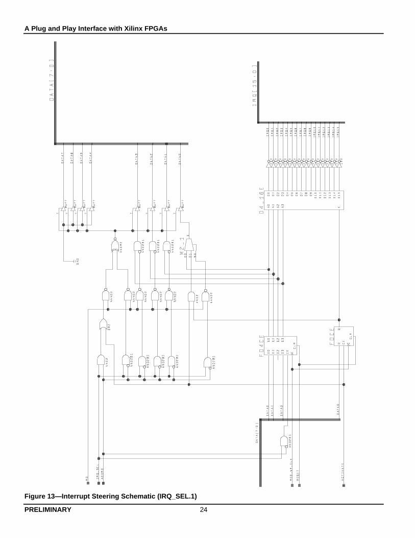
request logic is shown in Figure 13. The referencedesign only uses IRQ2 through IRQ5 though all 15are available.
The edge/level and high/low active state of the inter-rupt must be written to the Interrupt Request Typeregister. If no interrupt is assigned, the InterruptLevel Select register must be set to 0. The IRQ2signal on the ISA bus is routed to IRQ 9 on the 8259interrupt controller. To select IRQ 2 on the ISA bus,the Interrupt Level Select register must be set to 2,not 9.
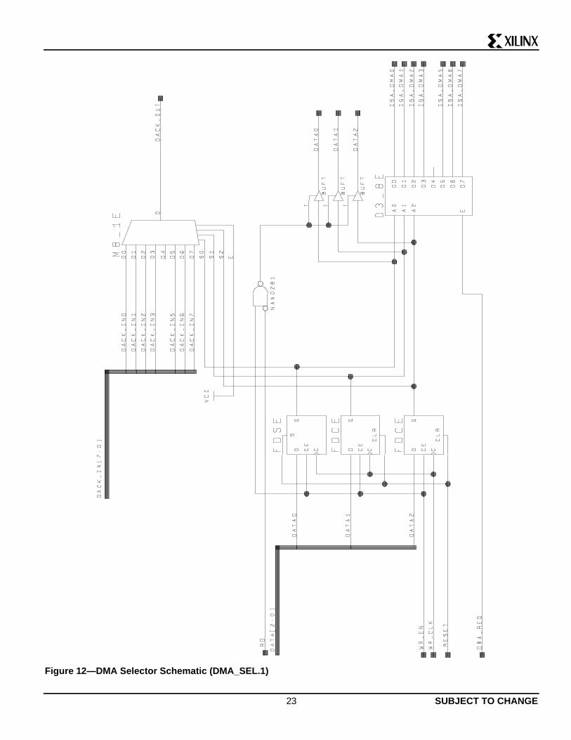
n DMA Channel — The DMA channel for a logicaldevice is selected by writing the DMA channel num-ber to the DMA Channel Select register. The DMAlogic is shown in Figure 12. The select number rep-resents the number of the DRQ/DACK channel onthe ISA bus. If no DMA channel is assigned, thisregister must be set to 4.
The last step in the programming sequence is to set thelogical device's activate bit. This forces the logical de-vice to become active on the ISA bus at its assignedresources. When finished programming configurationregisters, all cards must be set to the Wait for Keystate.
Run Time Access to Plug and Play registers
Read access to Plug and Play configuration is availableat all times with no impact to the function(s) on the card.However, write accesses to Plug and Play registersmust be done with the full knowledge of the devicedriver controlling the device and the operating systemenvironment. Even though it is possible to re-assign theCSNs during run time, this is not necessary since CSNsfor all Plug and Play cards are assigned during initiali-zation. The only exception to this case is for dockingstations, hot-insertion capability or if power manage-ment is supported. It is required that prior to changingthe value of any registers, the logical device be de-activated, the resource register re-programmed, and thelogical device is activated again. When finished access-ing Plug and Play registers, all cards must be returnedto the Wait for Key state.
High-Volume, Cost-Reduction Strategies
Plug and Play ISA cards typically will be shipped in highproduction volumes. While the Plug and Play ISAspecification is still in a state of flux, programmablelogic is probably the best solution for implementing theinterface.
However, as the specification matures, there are a fewstrategies for reducing the overall cost. In this applica-tion note, the design is implemented using an XC4003-6PQ100C. This provides a relatively low cost solutionwhile retaining the benefits of flexible, changeable pro-grammable logic. As of this writing (February 1995),Xilinx recently introduced a new FPGA family called the
11 SUBJECT TO CHANGE
XC5200. The attributes of the XC5200 family importantfor this design are:
n Pin-compatibility with corresponding XC4000 de-vices.
n A revolutionary, low-cost architecture by exploitingadvanced 0.6µ triple-layer metal CMOS technology.
This design can be migrated to the lower-cost XC5200,when available, without changing the PC board pinout.The XC5200 offers a cost reduction over the XC4003while remaining fully re-programmable.
Once the Plug and Play ISA specification has solidified,another option for higher-volume applications is to cov-ert the programmable XC4003 design into a mask-programmed Xilinx XC4303 or XC4403 HardWire™ gatearray. The HardWire gate array offers:
n 100% pin- and design-compatibility with the XC4003
n Low NRE charge
n “Design Once” — A low-risk conversion process us-ing the same design files as used in the XC4003without requiring test or simulation vectors
n 100% fault coverage without requiring user-writtentest vectors
n Reduced production costs
Using the Xilinx Plug and Play Design Files
This design is made available on diskette. This sectiondescribes what software is required to run the designand the steps involved. Also, please read through theLimitations and Restrictions section.
Software Requirements
The following software is required to process this design:
n PKUNZIP 2.04e, or later, unarchiving pro-gram.
n Xilinx XACT 5.0, or later, FPGA development sys-tem.
n VIEWdraw or VIEWdraw-LCA schematic editor withXilinx XC4000 Unified libraries. This is required inorder to make modifications to the schematics.
n Xilinx X-ABEL or Data I/O ABEL 5.0 or later. This isrequired in order to make modifications to the vari-ous state machine design implemented using ABEL.
n QBASIC BASIC intrepreter usually included with MS-DOS. This is only required for executing the variousBASIC test programs.
Using the Design on Your System
1. Create a new directory called PLGPLY on your harddisk.
2. Copy the file called PLUGPLAY.EXE into thePLGPLY directory.
3. Type PLUGPLAY.EXE on the command line. Thisextracts a README.TXT file, and a hierarchical ar-chive of the design files called PLGPLY.ZIP .
4. Invoke PKUNZIP -D PLYGPLY.ZIP to extract thefiles, including their hierarchical path names, ontoyour disk.
5. Edit the VIEWDRAW.INI file. Make sure that theVIEWlogic design library pointers are set appropri-ately for your machine. You will find the librarypointers near the end of the file.
6. Invoke the XDM program.
7. Set the part type for a XC4003-6PQ100C.
8. Run XMAKE on PLGPLY.MAK to process the design.The schematic files named PLGPLY.1 throughPLGPLY.3 include the top-level schematics.
Design Directories
The files are installed in separate sub-directories asshown in Table 2.
Table 2. Design Sub-directories.Sub-Directory Files
/SCH VIEWdraw schematic designs/SYM VIEWdraw symbols used in the
schematics/WIR VIEWdraw wire files/BASIC QBASIC routines used to test and
access the Plug and Play design/CMD VIEWsim command files for
simulation
Limitations and Restrictions
WARNING: THIS IS AN UNTESTED DESIGN.
Xilinx, Inc. does not make any representation or war-ranty regarding this design or any item based on thisdesign. Xilinx disclaims all express and implied warran-ties, including but not limited to the implied fitness ofthis design for a particular purpose and freedom frominfringement. Without limiting the generality of the fore-going, Xilinx does not make any warranty of any kindthat any item developed based on this design, or anyportion of it, will not infringe any copyright, patent, tradesecret or other intellectual property right of any personor entity in any country. It is the responsibility of theuser to seek licenses for such intellectual property rightswere applicable. Xilinx shall not be liable for any dam-ages arising out of or in connection with the use of thedesign including liability for lost profit, business interrup-tion, or any other damages whatsoever.
Design Support and Feedback
This application note, like the Plug and Play ISA specifi-cation itself, is still under development. Consequently,there will most likely be future changes and additions.
A Plug and Play Interface with Xilinx FPGAs
PRELIMINARY 12
If you would like to be updated with new versions of thisapplication note, or if you have questions, comments, orsuggestions, or if you discover potential problems,please send an E-mail to
or a FAX addressed to "Corporate Applications: Plugand Play Application Note" sent to
1+(408) 879-4442.
Updates to this document can be received via E-mail.Send an E-mail message to [email protected] withsend 21610 in the subject header.
IMPORTANT: Please be sure to include which versionof the application note you are using. The version num-ber is in the lower right-hand corner of page 1.
Additional Resources
The following additional information is available on Plugand Play:
Plug and Play ISA 1.0a Specification
Available via the ComuServe Plug and Play forum (GOPLUGPLAY). Requires a CompuServe account. Thespecification is available as a downloadable MicrosoftWord for Windows 6.0 .DOC file.
Plug and Play X-NOTES
Contains additional basic background information on thePlug and Play market and design solutions. Availablefrom your local Xilinx sales office.
Acknowledgments
Portions reprinted by permission of Intel Corporation,Copyright/Intel Corporation 1994.

13 SUBJECT TO CHANGE
NOTES:
A Plug and Play Interface with Xilinx FPGAs
PRELIMINARY 14
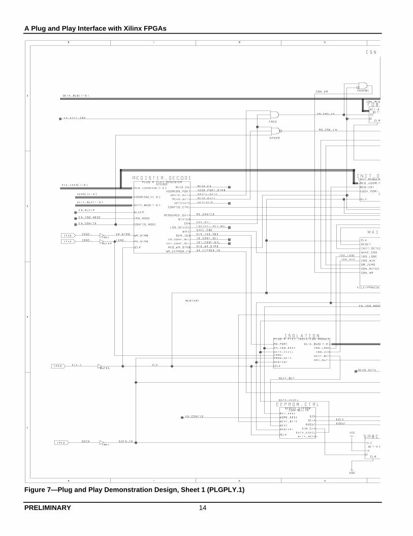
Figure 7—Plug and Play Demonstration Design, Sheet 1 (PLGPLY.1)
15 SUBJECT TO CHANGE
A Plug and Play Interface with Xilinx FPGAs
PRELIMINARY 16
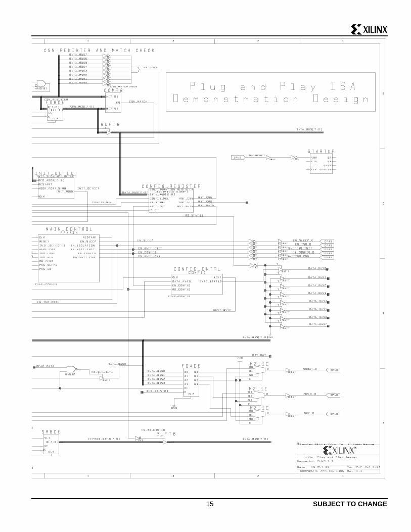
Figure 8—Plug and Play Demonstration Design, Sheet 2 (PLGPLY.2)
17 SUBJECT TO CHANGE
A Plug and Play Interface with Xilinx FPGAs
PRELIMINARY 18
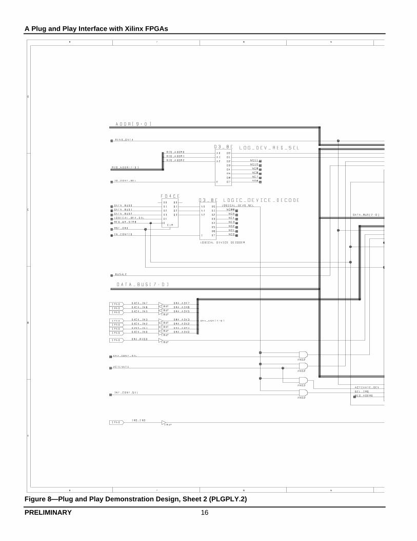
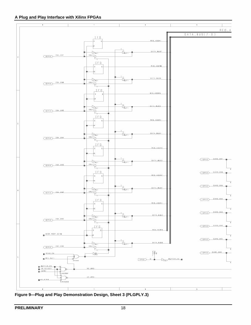
Figure 9—Plug and Play Demonstration Design, Sheet 3 (PLGPLY.3)
19 SUBJECT TO CHANGE
A Plug and Play Interface with Xilinx FPGAs
PRELIMINARY 20
Figure 10—Plug and Play Ports (PP_DEC.1)
21 SUBJECT TO CHANGE
A Plug and Play Interface with Xilinx FPGAs
PRELIMINARY 22
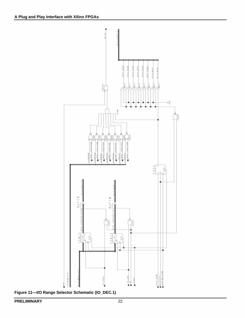
Figure 11—I/O Range Selector Schematic (IO_DEC.1)
23 SUBJECT TO CHANGE
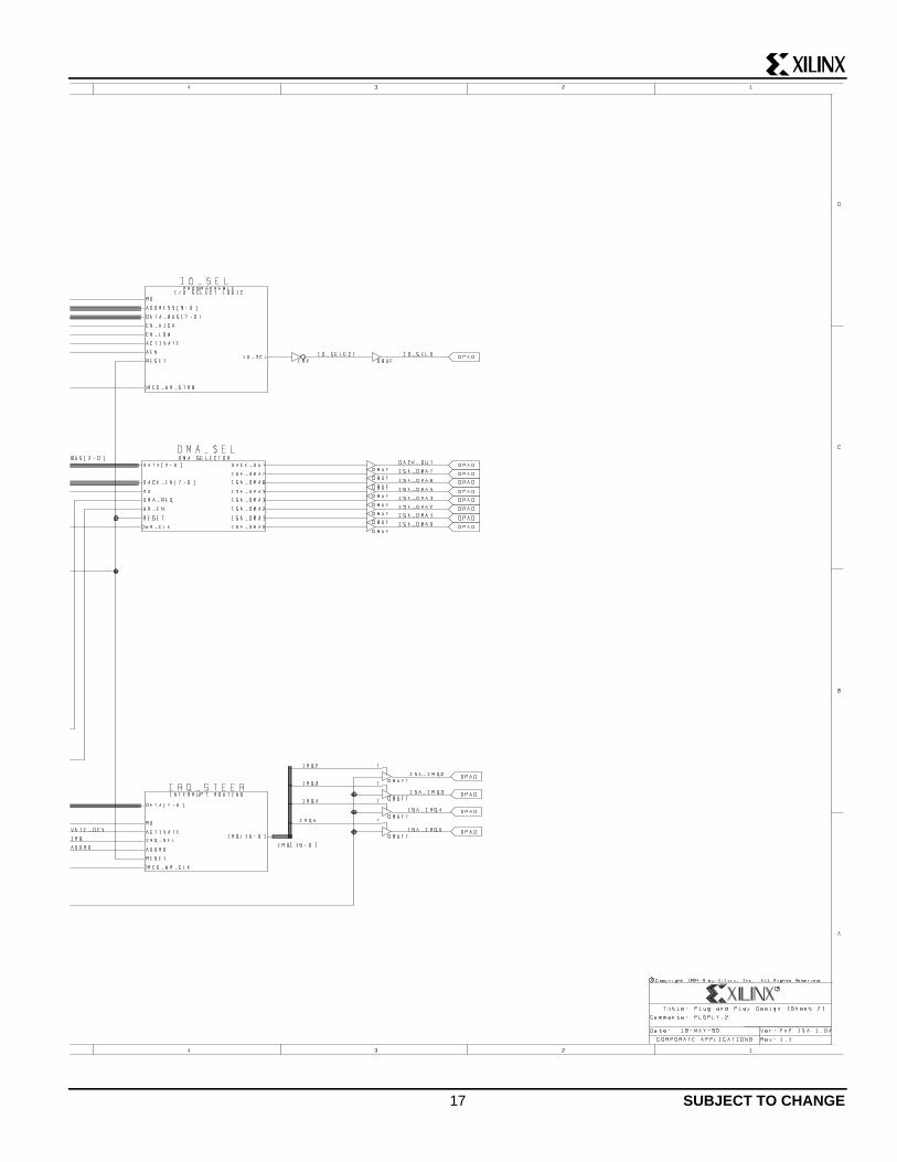
Figure 12—DMA Selector Schematic (DMA_SEL.1)
A Plug and Play Interface with Xilinx FPGAs
PRELIMINARY 24
Figure 13—Interrupt Steering Schematic (IRQ_SEL.1)
25 SUBJECT TO CHANGE
Figure 14—Configuration Register Schematic (CONF_REG.1)
A Plug and Play Interface with Xilinx FPGAs
PRELIMINARY 26
Figure 15—Isolation Protocol Schematic (ISO_MOD.1)
27 SUBJECT TO CHANGE
Figure 16—Isolation State Machine Listing (ISOLATE.ABL)
" Copyright (c) 1994 Xilinx, Inc.
module isolatetitle 'Plug & Play isolation state machine'
" clock clk pin;
" inputs iso_mode pin; "card in isolation mode
prom_data pin; "ID data one bit at a time bit_avail pin; "bit available from PROM
rd_port pin; "ISA I/O port read to isolation address
db_reg0 pin; "Registered databus bit 0 db_reg1 pin; "Registered databus bit 1
rd_cnt_cmp pin; "when 72 isolation reads completed goes true
restart pin; "signal used to force back to state s0
" outputs next_bit pin istype 'reg_D'; "requests another bit of data from PROM
db0 pin istype 'reg_D'; "output data 0 db1 pin istype 'reg_D'; "output data 1 drv_db pin istype 'reg_D'; "output enable for data bus driver
clr_iso_mode pin istype 'reg_D'; "clears the register that indicates in isolation mode clr_rd_cnt pin istype 'reg_D'; "isolation read count clear signal rd_cnt_inc pin istype 'reg_D'; "increment the isolation read counter
isolated pin istype 'reg_D'; "sucess -- 72 isolation reads done
" state diagram label definitions sbit STATE_REGISTER istype 'reg_D'; s0, s1, s2, s3, s4, s5, s6, s7, s8, s9, s10, s11, s12 STATE;
" The power-on initial state is 's0'xilinx property 'Initialstate s0';
" label definitions db_in =[db_reg1, db_reg0]; db_out =[db1, db0];
HIGH = 1; LOW = 0;
EQUATIONS
next_bit.clk = clk; db0.clk = clk; db1.clk = clk; drv_db.clk = clk; clr_iso_mode.clk = clk; clr_rd_cnt.clk = clk; rd_cnt_inc.clk = clk; isolated.clk = clk; sbit.clk = clk;
" STATE MACHINE DESCRIPTION" -------------------------" There are two main branches to this state machine, depending on the data" from the Serial Identification data in the PROM." When the PROM data is HIGH, then the state machine actively drives a
A Plug and Play Interface with Xilinx FPGAs
PRELIMINARY 28
" 0x55h pattern and then a 0xAAh pattern on the bus. Then the state" machine increments the isolation read counter and the isolation" sequence continues." When the PROM data is LOW, then the state machine monitors the data bus." If this card detects another card driving the bus with 0x55h followed" by 0xAAh, then this card drops out of the current isolation round (but" it will compete in the next round). If no other card is detected" driving the bus, then the read counter is incremented and the sequence" contiues."" Sucessful isolation is indicated by the ISOLATED signal going high."
State_Diagram sbit
ASYNC_RESET s0: restart;
" Wait for the card to be in ISOLATION mode." ----------------------------------------- state s0: if (!iso_mode) then s0 else s1 with next_bit := HIGH; endwith;
" Wait for data to be available from PROM." --------------------------------------- state s1: if (!bit_avail) then s1 with next_bit := HIGH; else s2;
" Wait for the system to read the PROM data. Jump to the appropriate loop" in the state machine depending on whether the PROM data is HIGH or LOW." If HIGH, then jump to state 's3' while driving 0x55h on the bus." Otherwise, jump to state 's6'." ------------------------------------------------------------------------- state s2: if (!rd_port) then s2 else if (rd_port & prom_data) then s3 with drv_db := HIGH; db_out := ^b01; " drive the bus with 0x55h endwith; else if (rd_port & !prom_data) then s6
" ==============================" SERIAL IDENTIFIER DATA IS HIGH" ==============================" WAIT for read cycle to end and continue to drive the bus with 0x55h." ------------------------------------------------------------------- state s3: if (rd_port) then s3 with drv_db := HIGH; db_out := ^b01; " drive bus with 0x55h endwith; else s4;
" WAIT for next read cycle but now drive the bus with 0xAAh." --------------------------------------------------------- state s4: if (!rd_port) then s4 else s5 with drv_db := HIGH; db_out := ^b10; endwith;
" Keep driving the bus with 0xAAh until the end of the read cycle. At the" end of the cycle, increment the read counter and proceed to state 's11'." ------------------------------------------------------------------------ state s5: if (rd_port) then s5 with drv_db := HIGH; db_out := ^b10; endwith; else s11 with rd_cnt_inc := HIGH; endwith;
29 SUBJECT TO CHANGE
" =============================" SERIAL IDENTIFIER DATA IS LOW" =============================" Check if another card is driving the bus with 0x55h data. If there is a" card driving 0x55h, then goto state 's7' and begin the check for 0xAAh." If no other card is driving 0x55h, then goto state 's9' to complete" this round." ------------------------------------------------------------------------- state s6: if (rd_port) then s6 else if (!rd_port & db_reg0 & !db_reg1) then s7 else s9;
" WAIT for next read cycle." ------------------------ state s7: if (!rd_port) then s7 else s8;
" Check if another card is driving the bus with 0xAAh data. If there is a" card driving 0xAAh, then drop out of the this isolation round and go" back to state 's0'." If no other card is driving 0xAAh, then goto state 's11' to complete" this round." ------------------------------------------------------------------------- state s8: if (rd_port) then s8 else if (!rd_port & !db_reg0 & db_reg1) then s0 with clr_rd_cnt := HIGH; clr_iso_mode := HIGH; endwith; else s11 with rd_cnt_inc := HIGH; endwith;
" WAIT for next read cycle. The data bus is not being driven with 0x55h." ---------------------------------------------------------------------- state s9: if (!rd_port) then s9 else s10;
" WAIT for read cycle to end, then get next bit from PROM." ------------------------------------------------------- state s10: if (rd_port) then s10 else s11 with rd_cnt_inc := HIGH; endwith;
" =================" CHECK IF ISOLATED" =================" Check to see if all 72 serial identifier reads have occured. If so, then" this card has been isolated. Otherwise, continue the isolation process." -------------------------------------------------------------------------- state s11: if (rd_cnt_cmp) then s11 with isolated := HIGH; endwith; else s12 with next_bit := HIGH; endwith;
" This state synchronizes the EEPROM controller's data_avail signal to this" this state machine." -------------------------------------------------------------------------- state s12: if (bit_avail) then s12 with next_bit := HIGH; endwith; else s1 with next_bit := HIGH; endwith;
end isolate
A Plug and Play Interface with Xilinx FPGAs
PRELIMINARY 30
Figure 17—ABEL source file for Plug and Play main state machine (PPMAIN.ABL).
" Copyright (c) 1994 Xilinx, Inc.
module ppmaintitle 'Plug & Play main control state machine';
" CLOCK clk pin;
" INPUTS reset pin; init_detected pin; wake_cmd pin; iso_lose pin; iso_win pin; db_zero pin; csn_match pin; csn_wr pin;
" OUTPUTS restart pin istype 'reg_D';
en_sleep pin; en_isolation pin; en_wait_init pin; en_config pin; en_wait_csn pin;
" STATE DEFINITIONS states STATE_REGISTER istype 'reg_D';
wait_init, sleep, iso_mode, wait_csn, config state;
" EQUATES HIGH = 1; LOW = 0;
" Set power-up initial state to 'wait_init'Xilinx Property 'InitialState wait_init';
EQUATIONS states.clk = clk; restart.clk = clk;
en_wait_init = wait_init; en_sleep = sleep; en_isolation = iso_mode; en_wait_csn = wait_csn; en_config = config;
State_Diagram states ASYNC_RESET wait_init: reset;
" STATE: WAIT FOR INITIATION KEY (wait_init)" -------------------------------------------" Plug and Play cards wake up in a queiscent state and wait for an initiation" key before becoming active. Once the initiated, the cards transition to" the SLEEP state.
state wait_init: if (!init_detected) then wait_initelse sleep;
31 SUBJECT TO CHANGE
" STATE: SLEEP (sleep)" --------------------" A card wakes up with its Card Select Number (CSN) set to zero. Once a card" is uniquely isolated, it is assigned a non-zero CSN identifier." Cards that have not been isolated will enter ISOLATION when the software" sends a WAKE[CSN] command with CSN=0." A card that has been isolated (i.e. CSN > 0) will enter the CONFIGURATION" state when the software sends a WAKE[CSN] command where CSN matches the" cards unique CSN." All other cards will remain in SLEEP.
state sleep: if (wake_cmd & db_zero & csn_match) then iso_mode with restart := HIGH; endwith; else if (wake_cmd & !db_zero & csn_match) then config with restart := HIGH; endwith; else sleep;
" STATE: ISOLATION" -----------------" Unisolated cards compete to win the isolation process using their serial" identification data." If a card loses during the current isolation round, it then goes back to" the SLEEP state." If a card wins, it goes to WAIT FOR CSN." If no winner is yet assigned, the card competes in the next isolation round.
state iso_mode: if (iso_lose) then sleep with restart := HIGH; endwith; else if (iso_win) then wait_csn else iso_mode;
" STATE: WAIT FOR CSN" --------------------" A uniquely isolated card waits for the software to assign the card its" unique Card Selection Number." After the CSN is written, the card enters the CONFIGURATION state.
state wait_csn: if (csn_wr) then config else wait_csn;
" STATE: CONFIGURATION" ---------------------" A card remains in the CONFIGURATION state until the software wishes to" wake another card (i.e. WAKE[CSN] with CSN <> card's CSN). When another" is awakened, this card will go back into the SLEEP state because only" one card can be in the CONFIGURATION state.
state config: if (wake_cmd & !csn_match) then sleep else config;
end ppmain;
A Plug and Play Interface with Xilinx FPGAs
PRELIMINARY 32
Figure 18—Initiation Key Schematic (INITKEY.1)
33 SUBJECT TO CHANGE
Figure 19—Initiation Key LFSR Schematic (LFSR_KEY.1)
A Plug and Play Interface with Xilinx FPGAs
PRELIMINARY 34
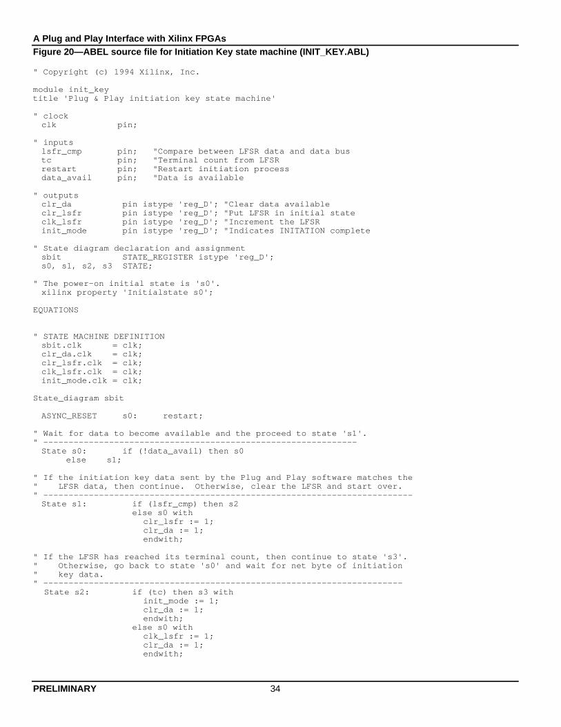
Figure 20—ABEL source file for Initiation Key state machine (INIT_KEY.ABL)
" Copyright (c) 1994 Xilinx, Inc.
module init_keytitle 'Plug & Play initiation key state machine'
" clockclk pin;
" inputslsfr_cmp pin; "Compare between LFSR data and data bustc pin; "Terminal count from LFSRrestart pin; "Restart initiation processdata_avail pin; "Data is available
" outputsclr_da pin istype 'reg_D'; "Clear data availableclr_lsfr pin istype 'reg_D'; "Put LFSR in initial stateclk_lsfr pin istype 'reg_D'; "Increment the LFSRinit_mode pin istype 'reg_D'; "Indicates INITATION complete
" State diagram declaration and assignmentsbit STATE_REGISTER istype 'reg_D';s0, s1, s2, s3 STATE;
" The power-on initial state is 's0'.xilinx property 'Initialstate s0';
EQUATIONS
" STATE MACHINE DEFINITIONsbit.clk = clk;clr_da.clk = clk;clr_lsfr.clk = clk;clk_lsfr.clk = clk;init_mode.clk = clk;
State_diagram sbit
ASYNC_RESET s0: restart;
" Wait for data to become available and the proceed to state 's1'." --------------------------------------------------------------
State s0: if (!data_avail) then s0else s1;
" If the initiation key data sent by the Plug and Play software matches the" LFSR data, then continue. Otherwise, clear the LFSR and start over." -------------------------------------------------------------------------
State s1: if (lsfr_cmp) then s2else s0 with
clr_lsfr := 1;clr_da := 1;endwith;
" If the LFSR has reached its terminal count, then continue to state 's3'." Otherwise, go back to state 's0' and wait for net byte of initiation" key data." -----------------------------------------------------------------------
State s2: if (tc) then s3 withinit_mode := 1;clr_da := 1;endwith;
else s0 withclk_lsfr := 1;clr_da := 1;endwith;

35 SUBJECT TO CHANGE
" Once the entire initation key has been read and verified, indicate that" the card is now in INITIATION mode." -----------------------------------------------------------------------
State s3: if (!data_avail) then s3 withinit_mode := 1;clr_lsfr := 1;endwith;
else s0;
end init_key
A Plug and Play Interface with Xilinx FPGAs
PRELIMINARY 36
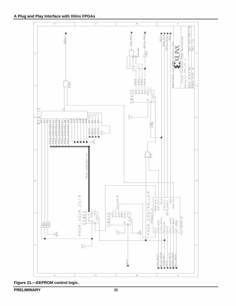
Figure 21.—EEPROM control logic.
37 SUBJECT TO CHANGE
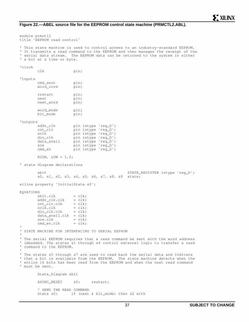
Figure 22.—ABEL source file for the EEPROM control state machine (PRMCTL2.ABL).
module prmctl2title 'EEPROM read control'
" This state machine is used to control access to an industry-standard EEPROM." It transmits a read command to the EEPROM and then manages the receipt of the" serial data stream. The EEPROM data can be returned to the system in either" a bit at a time or byte.
"clock clk pin;
"inputs cmd_sent pin; word_rcvd pin;
restart pin; next pin; next_word pin;
word_mode pin; bit_mode pin;
"outputs addr_clk pin istype 'reg_D'; cnt_clr pin istype 'reg_D'; sclk pin istype 'reg_D'; din_clk pin istype 'reg_D'; data_avail pin istype 'reg_D'; sce pin istype 'reg_D'; cmd_en pin istype 'reg_D';
HIGH, LOW = 1,0;
" state diagram declarations
sbit STATE_REGISTER istype 'reg_D'; s0, s1, s2, s3, s4, s5, s6, s7, s8, s9 state;
xilinx property 'InitialState s0';
EQUATIONS sbit.clk = clk; addr_clk.clk = clk; cnt_clr.clk = clk; sclk.clk = clk; din_clk.clk = clk; data_avail.clk = clk; sce.clk = clk; cmd_en.clk = clk;"" STATE MACHINE FOR INTERFACING TO SERIAL EEPROM"" The serial EEPROM requires that a read command be sent with the word address" imbedded. The states s1 through s4 control external logic to transfer a read" command to the EEPROM."" The states s5 through s7 are used to read back the serial data and indicate" that a bit is available from the EEPROM. The state machine detects when the" entire 16 bits has been read from the EEPROM and when the next read command" must be sent.
State_Diagram sbit
ASYNC_RESET s0: restart;
" SEND THE READ COMMAND state s0: if (next & bit_mode) then s2 with
A Plug and Play Interface with Xilinx FPGAs
PRELIMINARY 38
sce := HIGH; cmd_en := HIGH; endwith; else if (next_word & word_mode) then s2 with sce := HIGH; cmd_en := HIGH; endwith; else s0 with cnt_clr := HIGH; endwith;
state s2: goto s9 with sclk := HIGH; sce := HIGH; cmd_en := HIGH; endwith;
state s9: goto s3 with sce := HIGH; cmd_en := HIGH; endwith;
state s3: if (!cmd_sent) then s2 with sce := HIGH; cmd_en := HIGH; endwith; else s4 with sce := HIGH; cnt_clr := HIGH; addr_clk := HIGH; endwith;
" READ the data back out of the EEPROM a bit at a time state s4: goto s5 with sclk := HIGH; sce := HIGH; endwith;
state s5: if (next) then s6 with din_clk := HIGH; sce := HIGH; endwith; else if (next_word) then s7 with din_clk := HIGH; sce := HIGH; endwith;
state s6: if (next) then s6 with data_avail := HIGH; sce := HIGH; endwith; else s7 with data_avail := HIGH; sce := HIGH; endwith;
state s7: if (next_word & !word_rcvd & word_mode) then s4 with sce := HIGH; endwith; else if (next_word & word_rcvd & word_mode) then s7 with data_avail := HIGH; endwith; else if (!next & bit_mode) then s7 with data_avail := HIGH; sce := HIGH; endwith; else if (next & !word_rcvd & bit_mode) then s4 with sce := HIGH; endwith; else s0 with

39 SUBJECT TO CHANGE
cnt_clr := HIGH; endwith;
state s8: if (!next_word & word_mode) then s8 with data_avail := HIGH; endwith; else s0 with cnt_clr := HIGH; endwith;
end
Sales Offices
© 1995 Xilinx, Inc. All rights reserved. Xilinx and the Xilinx logo are registered trademarks, all XC-designated products are trademarks, and theProgrammable Logic Company is a service mark of Xilinx, Inc. All other company names are trademarks of their respective owners.
North America
Corporate Headquarters
Xilinx, Inc.2100 Logic DriveSan Jose, CA 95124U.S.A.
Tel: 1+(408) 559-7778FAX: 1+(408) 559-7114Web: http://www.xilinx.com/
Northern California
Xilinx, Inc.Oakmead Pkwy.Suite 202Sunnyvale, CA 95051
Tel: (408) 245-9850FAX: (408) 245-9865
Southern California
Xilinx, Inc.15615 Alton ParkwaySuite 280Irvine, CA 92718
Tel: (714) 727-0780FAX: (714) 727-3128
Colorado
Xilinx, Inc.5690 DTC ParkwaySuite 490WEnglewood, CO 80111
Tel: (303) 220-7541FAX: (303) 220-8641
New Hampshire
Xilinx, Inc.61 Spit Brook RoadNashua, NH 03060
Tel: (603) 891-1096FAX: (603) 891-0890
Pennsylvania
Xilinx, Inc.905 Airport Rd.Suite 200West Chester, PA 19380
Tel: (610) 430-3300FAX: (610) 430-0470
Texas
Xilinx, Inc.4100 McEwenSuite 237Dallas, TX 75244
Tel: (214) 960-1043FAX: (214) 960-0927
Illinois
Xilinx, Inc.939 N. Plum Grove RoadSuite HSchaumburg, IL 60173
Tel: (708) 605-1972FAX: (708) 605-1976
North Carolina
Xilinx, Inc.6080-C Six Forks RoadRaleigh, NC 27609
Tel: (919) 846-3922FAX: (919) 846-8316
Europe
United Kingdom
Xilinx, Ltd.Suite 1B, Cobb HouseOyster Lane, ByfleetSurry KT14 7DUUNITED KINGDOM
Tel: (44) 932-349401FAX: (44) 932-349499
France
Xilinx SarlEspace Jouy Technology21, rue Albert Calmette, Bt. C78353 Jouy en Josas CedexFRANCE
Tel: (33) 1-34-63-01-01FAX: (33) 1-34-63-01-09
Germany
Xilinx, GmbHDorfstr. 185609 AschheimMünchenGERMANY
Tel: (49) 89-904-5024FAX: (49) 89-904-4748
Japan
Xilinx, K.K.Daini-Nagaoka Bldg. 2F2-8-5, Hatchobori Chuo-kuTokyo 104JAPAN
Tel: (03) 3297-9191FAX: (03) 3297-9189
Asia Pacific
Hong Kong
Xilinx Asia PacificUnit No. 2318-2309Tower 1, MetroplazaHing Fong RoadKwai Fong, N.T.HONG KONG
Tel: (852) 2410-2717FAX: (852) 2494-7159E-mail: [email protected]
®
The Programmable Logic CompanySM