dram - circuits organization...
TRANSCRIPT
© 2015 TSMC, Ltd
DRAM -
Circuits
Organization
Interfaces
Shih-Lien Lu IEEE Microarchitecture Conference 2016
Acknowledgement: Dr. Shigeki Tomishima

© 2015 TSMC, Ltd 2
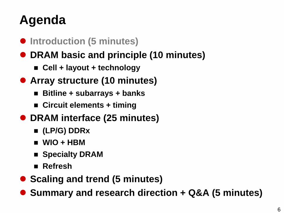
Agenda
Introduction (5 minutes)
DRAM basic and principle (10 minutes)
Cell + layout + technology
Array structure (10 minutes)
Bitline + subarrays + banks
Circuit elements + timing
DRAM interface (25 minutes)
(LP/G) DDRx
WIO + HBM
Specialty DRAM
Refresh
Scaling and trend (5 minutes)
Summary and research direction + Q&A (5 minutes)
© 2015 TSMC, Ltd 3
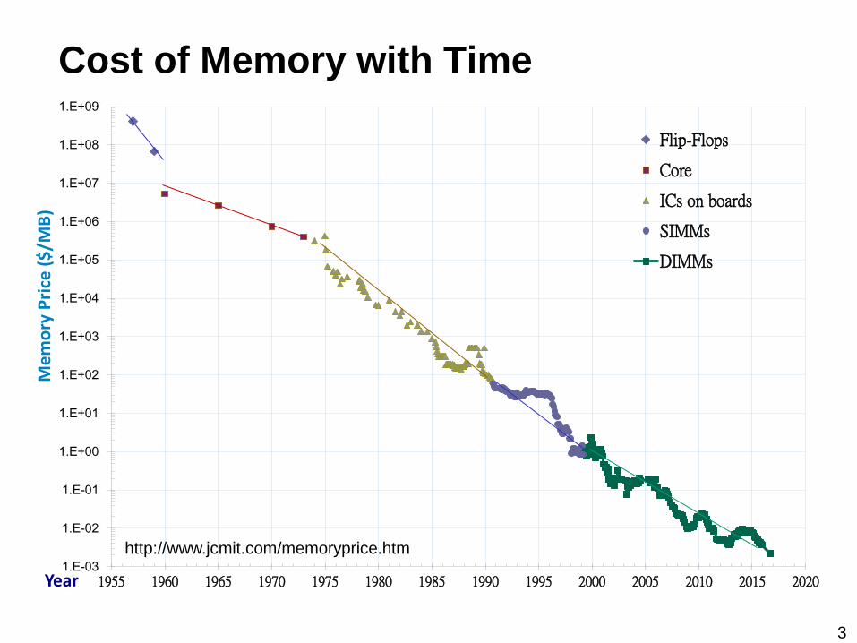
1.E-03
1.E-02
1.E-01
1.E+00
1.E+01
1.E+02
1.E+03
1.E+04
1.E+05
1.E+06
1.E+07
1.E+08
1.E+09
1955 1960 1965 1970 1975 1980 1985 1990 1995 2000 2005 2010 2015 2020
Me
mo
ry P
rice
($
/MB
)
Year
Flip-Flops
Core
ICs on boards
SIMMs
DIMMs
Cost of Memory with Time
http://www.jcmit.com/memoryprice.htm

© 2015 TSMC, Ltd 4
DRAM Scaling - Capacity
http://www.memcon.com/pdfs/proceedings2014/MOB102.pdf

© 2015 TSMC, Ltd 5
Introduction
Memory is a critical component
For more than 4 decades DRAM is the key
technology to implement main memory
Many amazing innovations lead to cost per bit reduction
143M folds in 41 years (1/2 cost every 18 months in avaerage)
Standardization of interface
Recent trends
Market segmentation
Technology challenges
Scaling slowing down?
Power?
DRAM internal modification?
Interface diversification + 3D
Reliability enhancement
© 2015 TSMC, Ltd 6
Agenda
Introduction (5 minutes)
DRAM basic and principle (10 minutes)
Cell + layout + technology
Array structure (10 minutes)
Bitline + subarrays + banks
Circuit elements + timing
DRAM interface (25 minutes)
(LP/G) DDRx
WIO + HBM
Specialty DRAM
Refresh
Scaling and trend (5 minutes)
Summary and research direction + Q&A (5 minutes)

© 2015 TSMC, Ltd 7
DRAM – Starting Out
An important invention
1968 patent by R. H. Dennard
1T1C cell
1970 W. Regitz ISSCC paper
3T cell
Intel 1103 (3T DRAM)
Introduced 1970
PMOS based
1st commercial 1Kb DRAM
Widely used by HP 9800 and PDP-11
K. Itoh, IEEE SSCS News, Winter 2008
G. Hendrie, “Oral History of Joel Karp,” Computer History Museum 2003
W. Regitz, J. Karp, “A three transistor-cell, 1024-bit, 500 NS MOS RAM,” IEEE JSSC 1970
The Intel Memory Design Handbook, August 1973
Intel Basic RAM Dynamic Cell
Read WL
Da
ta O
ut
Write WL
Da
ta In

© 2015 TSMC, Ltd 8
DRAM Development Innovations
Memory Cell
Planner Cap.
+
Planner Tr.
Stacked Cap. + Planner Tr.
Stacked Cap.
+
Recessed Tr. (RCAT-SRACT-URACT)
Trench Cap. + Planner Tr.
Sub-Array Architecture Technology
Open BL Folded BL Open BL
8F2 6F2
Cell Area
Interface Technology
Asynchronous Synchronous
DDRx, LPDDRx,
GDDRx, HBM
WIO, WIO2
(LRDIMM, FB-
DIMM, RDIMM)
4F2 22F2 16F2 4F2 (Elpida)
Many Innovations + Much Hard Work

© 2015 TSMC, Ltd 9
Cross Section View - Cartoon
Two areas
Array
Peripheral
Memory array area Standard logic area
Si Sub
M0 (W)
M2
M3
V2
V1
CH (W)
Si Surface
(Diffusion)
Poly Gate
Cell Capacitors
M0 CH
Cell Plate
WL
BL
STI
M1
© 2015 TSMC, Ltd 10
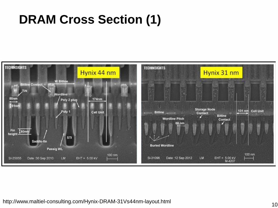
DRAM Cross Section (1)
http://www.maltiel-consulting.com/Hynix-DRAM-31Vs44nm-layout.html
© 2015 TSMC, Ltd 11
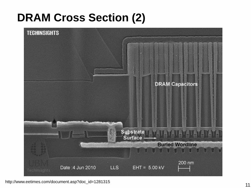
DRAM Cross Section (2)
http://www.eetimes.com/document.asp?doc_id=1281315

© 2015 TSMC, Ltd 12
DRAM Cross Section (3)
http://www.ma-tek.com/industry_detail.php?cpath=23

© 2014 TSMC, Ltd
13
TSMC Property
Destructive read Precharge bitline (BL) Fire wordline (WL) Develop a V diff
Vb=(CbVp+CsVs)/(Cs+Cb)
DVb=Vb-Vp is large enough for sensing
Write back Direct write
BL driven to high or low then forces in cell
Parameters Typical voltages
Vcca = 1.2V
Half Vcc = 0.6V
Vccp = 3.2V
Vbb = -0.6V
Vnwl = -0.3V
Capacitor Ta2O5
25-30fF
Access Transistor Characteristic Vt = ~0.9V
Id = ~10uA@cell
Ioff = ~10fA@cell
Cell Operation
WL (Vnwl ~ Vccp)
(1/2
Vc
ca
~ 0
V o
r Vc
ca
)
CP (1/2Vcca)
P-Well (Vbb)
BL

© 2014 TSMC, Ltd
14
TSMC Property
Cells EQ SA
Read Cross-couple latch SA
Timed enabling
Half-Vcc precharge
With equalization
Detect ~100mV diff
Vth imbalance sensitive
Write back Takes time to restore
Without full restoration cell charge deteriorates
Write Isolated by CSL
Cannot write all cells
Refresh Many rows each AR
Row address refresh
Read
Cell Operation
BL
BL#
SA
P
SA
N
LD
Q
…
EQ
Vcc/2
LD
Q#
CL_S A simplified ckt for folded bitline architecture
ISO
ISO
Data Write Sequence
1. BL (H)
2. WL (H) – On
3. WL (L) – Off
4. BL (M)
Data Read Sequence
1. BL (M)
2. WL (H) – On
3. BL (M+a) ; a=DVBL
4. WL (L) – Off

© 2015 TSMC, Ltd 15
DRAM Internal Timing
(Micron TN-40-03: DDR4 Networking Design Guide)
(WL likely under driven)
SA firing Equalize
Cells EQ SA BL
BL#
SA
P
SA
N
ISO
LD
Q
…
EQ
Vcc/2
ISO
LD
Q#
CL_S
Isolate
© 2015 TSMC, Ltd 16
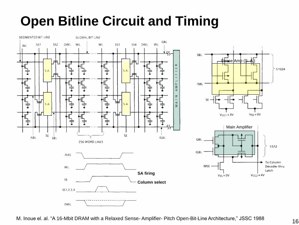
Open Bitline Circuit and Timing
M. Inoue el. al. “A 16-Mbit DRAM with a Relaxed Sense- Amplifier- Pitch Open-Bit-Line Architecture,” JSSC 1988
SA firing
Column select
Sense Amp (S. A.)
Main Amplifier

© 2015 TSMC, Ltd 17
Physical Layout
WL0 WL1
WL2 WL3
WL4 WL5
BL0
BL1
BL2
BL3
BL4
BL5
8F2 Cell (Folded BL Architecture) 6F2 Cell (Open BL Architecture)
3F
2F
T. Takahashi et. al. “A Multigigabit DRAM Technology With 6F2 Open-Bitline Cell, Distributed Overdriven Sensing, and Stacked-Flash Fuse,” JSSC 2001
S. Lu et. al. “Improving DRAM Latency with Dynamic Asymmetric Subarray,” IEEE Symp. On Microarchitecture, 2015
WL0 WL1
WL2 WL3
WL4 WL5
BL0
BL1
BL2
BL3
BL4
BL5
2
3
2
4

© 2015 TSMC, Ltd 18
Agenda
Introduction (5 minutes)
DRAM basic and principle (10 minutes)
Cell + layout + technology
Array structure (10 minutes)
Bitline + subarrays + banks
Circuit elements + timing
DRAM interface (25 minutes)
(LP/G) DDRx
WIO + HBM
Specialty DRAM
Refresh
Scaling and trend (5 minutes)
Summary and research direction + Q&A (5 minutes)

© 2015 TSMC, Ltd 19
DRAM Device Block Diagram
SRC: Micron TN4605.pdf
Core Array
Y-Control (Column)
CLK/CMD Inputs
Address Inputs
Data IO
2 Meg x 4 Memory Array with SDR and DDR Interface
© 2015 TSMC, Ltd 20
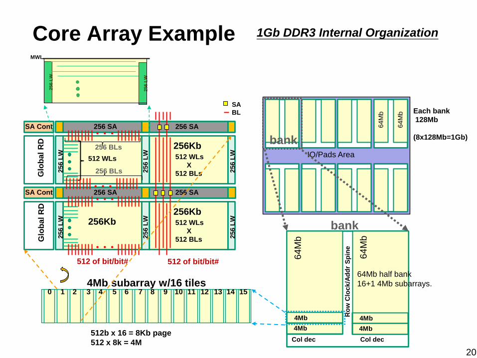
Core Array Example
64Mb half bank
16+1 4Mb subarrays. 4Mb subarray w/16 tiles
256 SA
256Kb
512 WLs
256 L
W
256 L
W
256 L
W
512 WLs
X
512 BLs 256 BLs
256 SA 256 SA
256 SA
Glo
bal
RD
256 BLs
256Kb
256 L
W
256 L
W
256 L
W
512 WLs
X
512 BLs Glo
bal
RD
SA Cont
SA Cont
256Kb
SA
BL
0 1 2 3 4 5 6 7 8 9 10 11 12 13 14 15
512b x 16 = 8Kb page
512 x 8k = 4M
64M
b
64M
b
IO/Pads Area
Col dec Col dec
Ro
w C
lock/A
dd
r S
pin
e
4Mb
1Gb DDR3 Internal Organization
64
Mb
64
Mb
Each bank
128Mb
(8x128Mb=1Gb) bank
bank
4Mb
4Mb
4Mb
512 of bit/bit# 512 of bit/bit#
256 L
W
256 L
W
MWL
© 2015 TSMC, Ltd 21
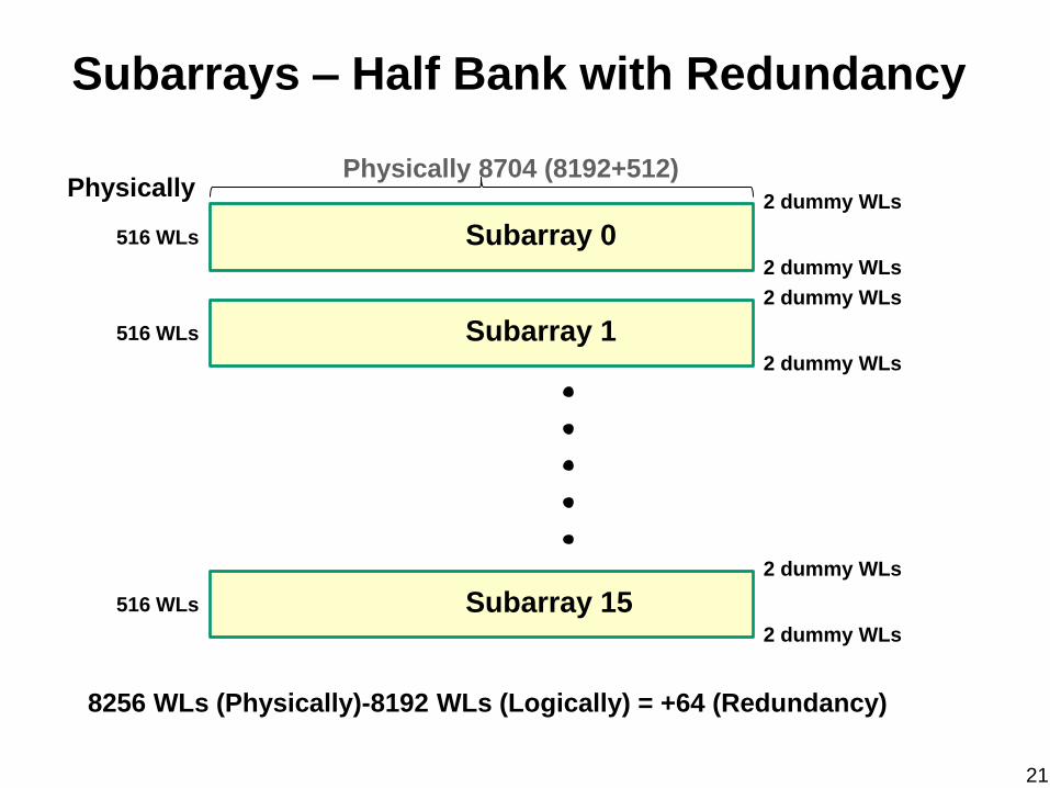
Subarrays – Half Bank with Redundancy
516 WLs
2 dummy WLs
2 dummy WLs
Subarray 0
516 WLs
2 dummy WLs
2 dummy WLs
Subarray 1
516 WLs
2 dummy WLs
2 dummy WLs
Subarray 15
8256 WLs (Physically)-8192 WLs (Logically) = +64 (Redundancy)
Physically Physically 8704 (8192+512)

© 2015 TSMC, Ltd 22
Subarrays/Tiles S
ub
arr
ay 0
Su
barr
ay 1
Su
barr
ay 2
Su
barr
ay 3
Su
barr
ay 4
Su
barr
ay 5
Su
barr
ay 6
Su
barr
ay 7
Su
barr
ay 8
Su
barr
ay 9
Su
barr
ay 0
’
T B T B T B T B T B T
SA
SA
SA
SA
Normal Subarrays
Edge Subarrays
SA SA SA SA SA SA
SA
SA
SA
SA
SA
SA
Subarray 0
Subarray 1
Subarray 0’
BL
BL#
BL
BL#
BL
BL#
Subarray i
Subarray i+1
Half row buffer
SA SA SA SA SA SA Half row buffer

© 2015 TSMC, Ltd 23
Cells to Chip
OPEN BL Architecture
SA
BL
BL#
Subarray 0
Subarray 1
LA GA
Local Amp Global Amp
DQ
Tx/Rx
DQ
Memory Array
DRAM Chip
WL0
WL524
RED : True Path
BLUE : Complement Path
Even data is “1” at DQ,
Physical charge in the memory cell depends on which subarray

© 2015 TSMC, Ltd 24
Detailed Signal Path
SA
SA
SA
SA
SA
SA
Subarray0 Subarray1 Subarray2
BL
BL
#
BL
B#
L
SA
SA
SA
SA
SA
SA
Subarray14 Subarray15 Subarray0
BL
BL
#
BL
BL
#
SA
S
A
SA
SA
S
A
SA
Half Normal
Half Dummy
HV
cc
HV
cc
SA
BL BL#
WLa
LIO
LIO# 1st
Amp
GIO GIO#
2nd
Amp
Tx
Rx
CS0
DQ Rd
(True)
Write
Driver Wd
(True)
WLb
Cell BL /BL LIO /LIO GIO /GIO Rd DQ
WLa H H L H L H H H L
WLb L H L H L H H H L
Half Normal
Half Dummy
RED : True
BLUE : Bar
Data Status at DQ Pins is not always equal to Data Status at Cells.

© 2015 TSMC, Ltd 25
1K Col dec.
Ro
w C
on
tro
l/A
dd
Sp
ine
64
Mb
4Mb
4Mb
4Mb
EX: M3 (AL) : ~2700um
Ctotal = ~0.6pF + 10% (Cg)
Rtotal =~700 Ohm
In the case of x8 DDR3
1:128 decode
64bits come out@ each 4Mb w/8 burst
CSL is common to all subarrays
64
Mb
64
Mb
IO/Pads Area
CSL (Column Select Line) Architecture

© 2015 TSMC, Ltd 26
Coldec.
256 SA
256Kb
256 L
WD
256
LW
D
257
6 L
WD
512 WLs
X
512 BLs
256 SA 256 SA
256 SA
Glo
bal
RD
SA Cont
SA Cont
LIO Pair 4b
LIO Pair 4b
GIO Pair 4b GIO Pair 4b GIO Pair 4b
32 SA Bands and
33 4Mb sub-arrays. 32 SA Bands and
33 4Mb sub-arrays.
Coldec.
GA GA GA
Col Dec.
GA : Global Amplifier
SA
BL
LA : Local Amplifier
- Many circuit variaty
- Voltage Sensing
- Write Path has MUX gate
- Many variations
- Vcc Precharge & Pull-down
- Voltage/Current Sensing
- Write Path has Write Driver
LIO : Local IO Pair
- Half-Vcc Precharge at Std-by
- After Subarray is selected,
Vcc Precharge & Pull-down
GIO : Global IO Pair - Vcc Precharge & Pull-down
IO Line Architecture

© 2015 TSMC, Ltd 27
Circuit Elements and Operation
Decoder
Wordline driver
Column muxing
Local to global bitline
Where does it make sense to add logic?

© 2015 TSMC, Ltd 28
DRAM Timing
Addr decode Signal devel & sensing Data out
Addr decode Signal devel & sensing & recovery Precharge
tRC = tRAS + tRP
Ac
tiva
te W
L
CMD/ADD
Decoding
Redundancy
SA
Fir
e CS
L F
ire
SA
Flip
By N
ew
Wri
te
BL
“H
” t
o ~
98
%
WL
Close
BL Equalize
BL
Pa
ir S
plit
to
ce
rta
in %
ACT
PRE
T3
RAED tRCD
WRITE tWR
T2
T1
tRAS > tRCD + T1 + tWR – T2 – T3
tAC

© 2015 TSMC, Ltd 29
DRAM Interface Timing Parameters (1)
tCL (or tCAS - CAS Latency)
This is the most important memory timing. CAS stands for Column Address Strobe. If a row has already been selected, it
tells us how many clock cycles we'll have to wait for a result (after sending a column address to the RAM controller).
tCCD (Column Address to Column Address Delay)
This is the minimum number of cycles between consecutive column accesses (CAS) to the same row.
tRCD (Row Address (RAS) to Column Address (CAS) Delay)
Once we send the memory controller a row address (through RAS), we'll have to wait this many cycles before accessing
one of the row's columns. So, if a row hasn't been selected, this means we'll have to wait tRCD + tCL cycles to get our
result from the RAM.
tRP (Row Precharge Time)
If we already have a row selected, we'll have to wait this number of cycles before selecting a different row. This means it
will take at least tRP + tRCD + tCL (tRC) cycles to access the data in a different row.
tRAS (Row Active Time)
This is the minimum number of cycles that a row has to be active for to ensure we'll have enough time to access the
information that's in it. This usually needs to be greater than or equal to the sum of two previous defined latencies (tRAS
>= tCL + tRCD)
tRC (Random Cycle Time or Row Cycle Time)
This is the time in cycles between two accesses from different rows in the same bank. In other word the time between
two successive ACTIVE commands to the same bank. (tRC=tRAS+tRP=tCL+tRCD+tRP)
tRRD (Row Active to Row Active Delay)
The minimum time interval in cycles between two successive ACTIVE commands to the different banks is defined by
tRRD.

© 2015 TSMC, Ltd 30
DRAM Interface Timing Parameters (2)
tWR (Write Recovery Time)
This is the number of clock cycles taken between writing data and issuing the pre-charge command. tWR is necessary to
guarantee that all data in the write buffer can be safely written to the memory core.
tRD (Read Delay)
This is the number of memory clocks from DRAM Chip Select# assert to data ready.
tWTR (Write to Read command Delay / Write to Read Delay)
This specifies the number of clock between the last valid write operation and the next read command to the same
internal bank.
tRTW (Read to Write delay)
This is the number of cycles needed to be inserted between read command and a subsequent write command on
different rank for data turn-around.
tRTP (Read to Precharge Delay)
Number of clocks inserted between a read command to a row pre-charge command to the same rank.
tFAW (Four Activate Window Time)
This specifies the time window in which four activates are allowed the same rank.
tRFC (Refresh Cycle Time)
This is the number of cycles needed to perform a refresh. As soon as the tRFC time elapses, the memory controller can
issue four consecutive Activate commands to different banks in the rank.
tREFI (Refresh Interval Time)
It is the window of time for each refresh command so DRAM cell does not lose its charge and corrupt. Its value depends
on capacity and number of rows in a bank and is measured in micro-seconds (µsec)
© 2015 TSMC, Ltd 31
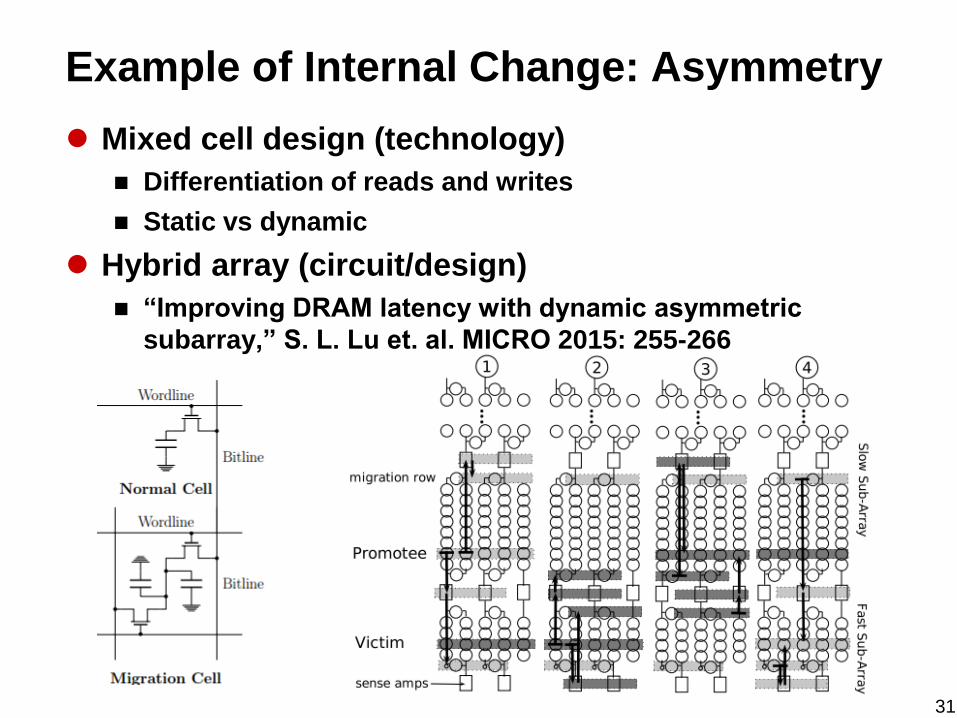
Example of Internal Change: Asymmetry
Mixed cell design (technology)
Differentiation of reads and writes
Static vs dynamic
Hybrid array (circuit/design)
“Improving DRAM latency with dynamic asymmetric
subarray,” S. L. Lu et. al. MICRO 2015: 255-266
© 2015 TSMC, Ltd 32
Agenda
Introduction (5 minutes)
DRAM basic and principle (10 minutes)
Cell + layout + technology
Array structure (10 minutes)
Bitline + subarrays + banks
Circuit elements + timing
DRAM interface (25 minutes)
(LP/G) DDRx
WIO + HBM
Specialty DRAM
Refresh
Scaling and trend (5 minutes)
Summary and research direction + Q&A (5 minutes)
© 2015 TSMC, Ltd 33
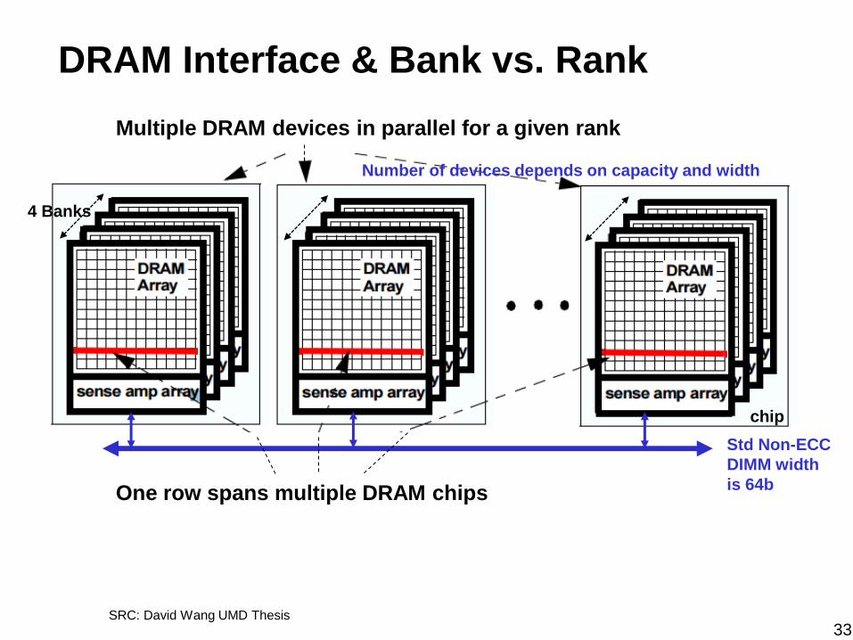
DRAM Interface & Bank vs. Rank
SRC: David Wang UMD Thesis
4 Banks
Multiple DRAM devices in parallel for a given rank
One row spans multiple DRAM chips
chip
Std Non-ECC
DIMM width
is 64b
Number of devices depends on capacity and width

© 2015 TSMC, Ltd 34
DRAM Std Bandwidth Trends
PF4X
DDR
0.4
0.8
>30
13.5
150
4
DDR2
0.8
1.6
30
6.75
50
4
DDR3
1.6
3.2
27.5
6.25
48
8
DDR4
3.2
6.4
27.5
5.75
34
8
WIO
0.2
12.8
>30
4
34
4
BW growth of SDR, DDR, DDR2,DDR3 comes
from prefetch factor and IO frequency, row
address access remain relatively the same
WIO2
0.8+
51.2
>30
NA
~10
8
BW increases from DDRx to WIO to
HBM due to wider DQs and higher
frequency
HBM
1.0
128*
30
4
~5
8/ch
Parameters
Data Rate
(GT/s)
Bandwidth
(GB/s)
Latency (ns)
Random
Access (ns)
Active
Energy(pJ/b)
Bank No.
512
IO
1024*
IO
Bank
Group
Prefetch
(PF)
2X
PF
2X
SRC: Joe Ting, Piecemakers

© 2015 TSMC, Ltd 35
ACT : Row Activation
PRE : Row Precharge
READ : Data Read
WRITE : Data Write
Primary Command (Row Operation)
(Col. Operation)
Idle Mode
Row Mode
Row Mode
Column Mode
Simplified DRAM Device State Diagram
Micron DDR3 Datasheetarge
Secondary Command

© 2015 TSMC, Ltd 36
DDR2/3 Command Truth Table Row Col WR
Command and Address pins are DDR

© 2015 TSMC, Ltd 37
?n-Prefetch of DDRx
SRC: Micron Technical Note TN-46-05
DDR
DDR
DDR2 is 4n-Prefetch
DDR3/4 is 8n-Prefetch
LPDDR4 is 16n-Prefetch
DDR2 has a prefetch buffer of depth 4
DDR3/4 has a prefetch buffer of depth 8
LPDDR4 has a prefetch buffer of depth 16

© 2015 TSMC, Ltd 38
DDR READ Example
SRC: Micron Technical Note TN-46-05
© 2015 TSMC, Ltd 39
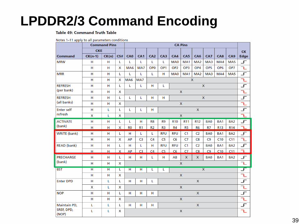
LPDDR2/3 Command Encoding

© 2015 TSMC, Ltd 40
LPDDR4 Command Table

© 2015 TSMC, Ltd 41
Agenda
Introduction (5 minutes)
DRAM basic and principle (10 minutes)
Cell + layout + technology
Array structure (10 minutes)
Bitline + subarrays + banks
Circuit elements + timing
DRAM interface (20 minutes)
(LP/G) DDRx
WIO + HBM
Specialty DRAM
Refresh
Scaling and trend (10 minutes)
Summary and research direction + Q&A (5 minutes)

© 2015 TSMC, Ltd 42
LPDDRx/WIOx/GDDRx
DDRx chips put in DIMMs usually
LPDDRx direct bond
Wider IO
WIOx
Multiple channels
For stacking with APU/CPU directly
GDDRx
Higher frequency
Direct bond

© 2015 TSMC, Ltd 43
High Bandwidth Memory
Stacked DRAM for graphics and HPC
Spec overview
2 channels per die (ec channel is similar to std DDR)
128b data IOs (DDR) per channel
500Mhz – 1GHz clock translate to 16–32 GB/s BW per ch
Up to 8 dice stack with each die 8Gb (2nd Gen)
New features
Per-bank refresh
Temperature compensated self-refresh
DBI
ECC support (optional)
JEDEC Std
Vs. HMC (Micron version of 3D stacked DRAM)

© 2015 TSMC, Ltd 44
HBM with 4 DRAM dice and 1 Logic Die
SRC: D.U Lee, JSSCC Jan. 2015

© 2015 TSMC, Ltd 45
Specialty DRAM - RLDRAM (vs. LRDIMM)
RLDRAM (Reduced Latancy DRAM)
Low tRC at the cost of density
SRAM-like interface (not address multiplexing)
RLDRAM-II
576Mb (x9, x18, x36)
400-533 MHz clk
BL=2
tRC = 15ns (6 or 8 cycles)
4GB/s BW max
LRDIMM (Load-Reduce DIMM)
Larger capacity
Multiple
Buffered cmd/addr and data
SRC: Micron RLDRAM datasheet and Inphi whitepaper
(https://www.inphi.com/products/whitepapers/Inphi_LRDIMM_whitepaper_Final.pdf)
© 2015 TSMC, Ltd 46
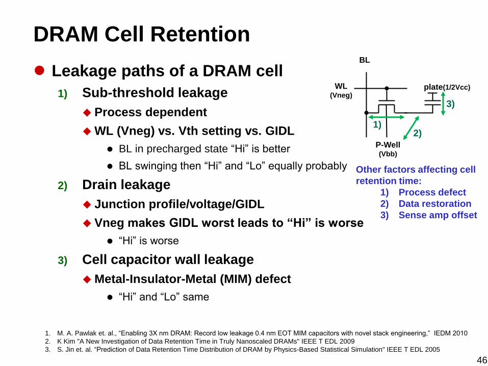
DRAM Cell Retention
Leakage paths of a DRAM cell
1) Sub-threshold leakage
Process dependent
WL (Vneg) vs. Vth setting vs. GIDL
BL in precharged state “Hi” is better
BL swinging then “Hi” and “Lo” equally probably
2) Drain leakage
Junction profile/voltage/GIDL
Vneg makes GIDL worst leads to “Hi” is worse
“Hi” is worse
3) Cell capacitor wall leakage
Metal-Insulator-Metal (MIM) defect
“Hi” and “Lo” same
Other factors affecting cell
retention time:
1) Process defect
2) Data restoration
3) Sense amp offset
WL (Vneg)
BL
plate(1/2Vcc)
P-Well (Vbb)
1) 2)
3)
1. M. A. Pawlak et. al., “Enabling 3X nm DRAM: Record low leakage 0.4 nm EOT MIM capacitors with novel stack engineering,” IEDM 2010
2. K Kim "A New Investigation of Data Retention Time in Truly Nanoscaled DRAMs" IEEE T EDL 2009
3. S. Jin et. al. “Prediction of Data Retention Time Distribution of DRAM by Physics-Based Statistical Simulation" IEEE T EDL 2005

© 2015 TSMC, Ltd 47
Full Array SR Power = Idd2 (DC + leak) + Full Array Refresh
1/16 SR Power = Idd2 (DC + Leak) + 1/16 Array Refresh
410uA
200uA
1650uA
575uA
Self Refresh Power = Idd2 (DC including Leak) + Refresh Power
Idd2 = 186uA
Ref. Power = 224uA
Idd2 = 504uA
Ref. Power = 1146uA
730uA
300uA
Idd2 = 272uA
Ref. Power = 458uA
LPDDR has TCSR
2Gb Mobile LPDDR SDR (src : Micron)

© 2015 TSMC, Ltd 48
DRAM Refresh
Needs to issue refresh periodically (tREFI) and each
time refresh takes tRFC
tRFC/tREFI unavailable (ex. 350/7800=4.5%)
AR vs. SR (SDRAM)
AR (auto-refresh) : issue AR command (RAS/CAS/CS all
asserted) no address needed (internal counter)
Opened rows are precharged before AR issued
Per-bank (LPDDRx) vs. all-bank
SR (self-refresh) : DRAM enters/exits SR mode
All banks pre-charged before entering
CKE low and RAS/CAS/CS low and WE high
tREFI (refersh interval – retention_time/refreshes)
(e.g. 64ms/8192 = 7.8ms)
tRFC (refresh cycle time – depends on DRAM chip density ~350ns for 8Gb)
Red/write access ~50ns

© 2015 TSMC, Ltd 49
Agenda
Introduction (5 minutes)
DRAM basic and principle (10 minutes)
Cell + layout + technology
Array structure (10 minutes)
Bitline + subarrays + banks
Circuit elements + timing
DRAM interface (25 minutes)
(LP/G) DDRx
WIO + HBM
Specialty DRAM
Refresh
Scaling and trend (5 minutes)
Summary and research direction + Q&A (5 minutes)
© 2015 TSMC, Ltd 50
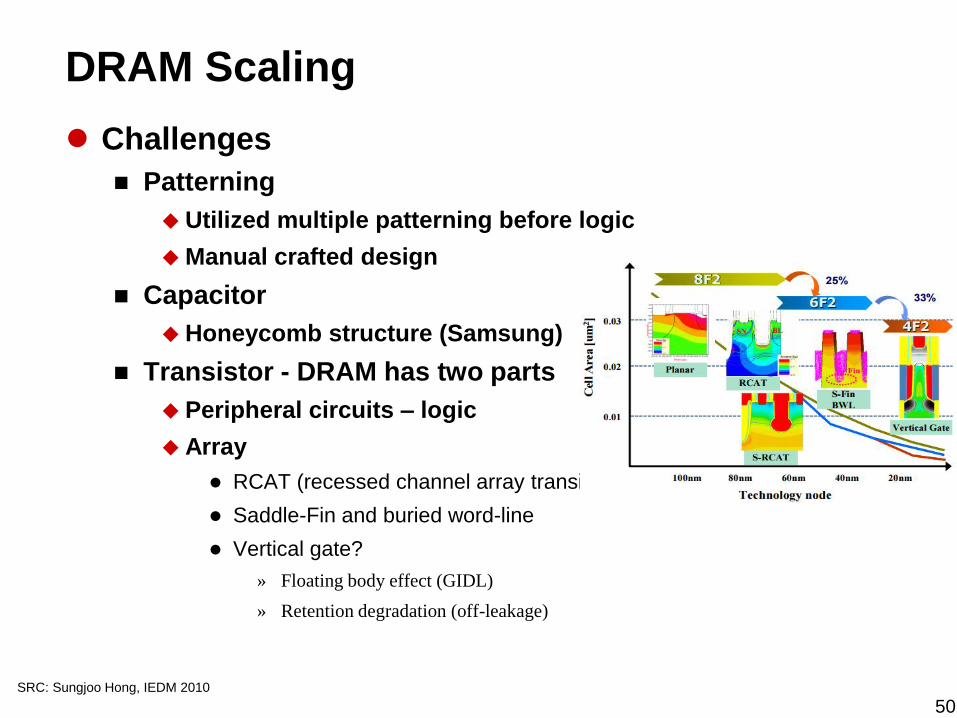
DRAM Scaling
Challenges
Patterning
Utilized multiple patterning before logic
Manual crafted design
Capacitor
Honeycomb structure (Samsung)
Transistor - DRAM has two parts
Peripheral circuits – logic
Array
RCAT (recessed channel array transistor)
Saddle-Fin and buried word-line
Vertical gate?
» Floating body effect (GIDL)
» Retention degradation (off-leakage)
SRC: Sungjoo Hong, IEDM 2010
© 2015 TSMC, Ltd 51
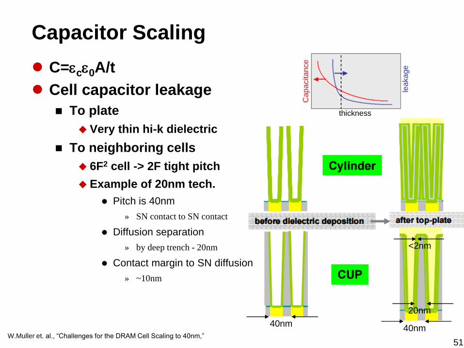
Capacitor Scaling
C=ece0A/t
Cell capacitor leakage
To plate
Very thin hi-k dielectric
To neighboring cells
6F2 cell -> 2F tight pitch
Example of 20nm tech.
Pitch is 40nm
» SN contact to SN contact
Diffusion separation
» by deep trench - 20nm
Contact margin to SN diffusion
» ~10nm
W.Muller et. al., “Challenges for the DRAM Cell Scaling to 40nm,”
40nm 40nm
20nm
<2nm
thickness
Cap
acita
nce
lea
ka
ge

© 2015 TSMC, Ltd 52
Scaling and Trend
Challenges
Interconnect
Capacitance of bitline – Cb/Cs ratio
Low-k spacer materials or air-gap?
Resistivity of bitline
Power/energy (active and stdby)
Density leads to over activation
Reliability
Variable retention
Disturb
Delay/timing
Security
Flipping bits
Data reminisce

© 2015 TSMC, Ltd 53
Redundancy (1)
Essential for yield improvement
Both row and column redundancy were employed early
Masashi Horiguchi, “Redundancy Techniques for High-Density DRAMs,” IEEE Int.
Conf. Innovative Systems Silicon, 1997
conventional
Simultaneous
replacement
Individual subarray
replacement
Flexible intra-subarray
replacement redundancy
© 2015 TSMC, Ltd 54
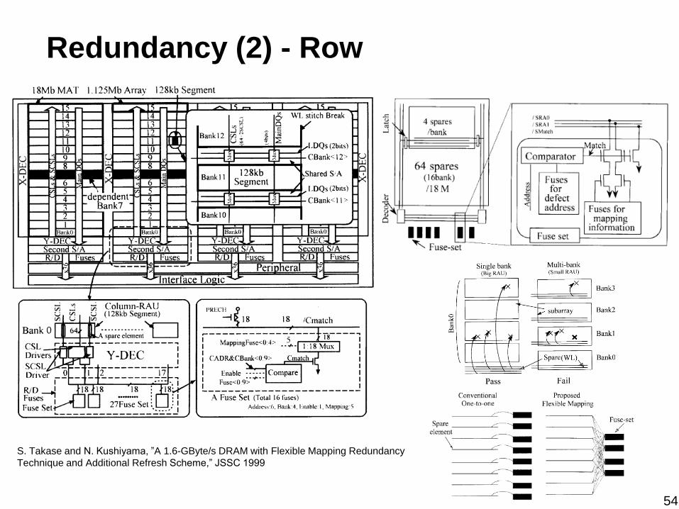
Redundancy (2) - Row
S. Takase and N. Kushiyama, ”A 1.6-GByte/s DRAM with Flexible Mapping Redundancy
Technique and Additional Refresh Scheme,” JSSC 1999

© 2015 TSMC, Ltd 55
On-Die ECC
First published paper
“A 50-11s 16-Mb DRAM with a 10-ns Data Rate and On-Chip
ECC” by Howard Kalter et. al. from IBM (JSSC 1990 )
Synergistic fault tolerant approach with row/column
redundancy
LPDDR4 (1st commodity DRAM) adopted on-die ECC
“A 3.2 Gbps/pin 8 Gbit 1.0 V LPDDR4 SDRAM With
Integrated ECC Engine for Sub-1 V DRAM Core Operation”
by Tae-Young Oh et. al. from Samsung (JSSC 2015)
SEC (not SECDED) (136, 128) code
Overhead is 6.25% in core array
With array efficiency ~50% the overhead is ~3%
Encoding overhead is 3ns (tWR from 15 to 18ns) vs LPDDR3
Decoding overhead is 2.5ns (RL from 15 to 17.5ns) vs LPDDR3

© 2015 TSMC, Ltd 56
LPDDR3 vs LPDDR4
“A 3.2 Gbps/pin 8 Gbit 1.0 V LPDDR4 SDRAM With Integrated ECC Engine for Sub-1 V DRAM Core Operation” by Tae-Young Oh et. al.
from Samsung (JSSC 2015)

© 2015 TSMC, Ltd 57
Bank Organization with Integrated ECC
“A 3.2 Gbps/pin 8 Gbit 1.0 V LPDDR4 SDRAM With Integrated ECC Engine for Sub-1 V DRAM Core Operation” by Tae-Young Oh et. al.
from Samsung (JSSC 2015)
© 2015 TSMC, Ltd 58
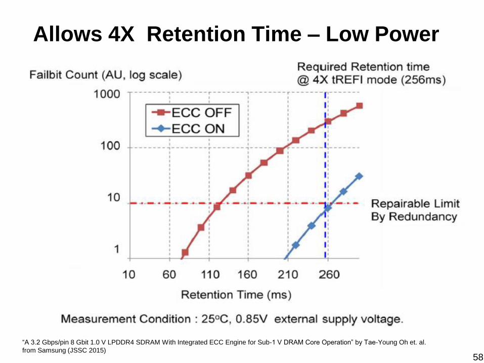
Allows 4X Retention Time – Low Power
“A 3.2 Gbps/pin 8 Gbit 1.0 V LPDDR4 SDRAM With Integrated ECC Engine for Sub-1 V DRAM Core Operation” by Tae-Young Oh et. al.
from Samsung (JSSC 2015)

© 2015 TSMC, Ltd 59
Agenda
Introduction (5 minutes)
DRAM basic and principle (10 minutes)
Cell + layout + technology
Array structure (10 minutes)
Bitline + subarrays + banks
Circuit elements + timing
DRAM interface (25 minutes)
(LP/G) DDRx
WIO + HBM
Specialty DRAM
Refresh
Scaling and trend (5 minutes)
Summary and research direction + Q&A (5 minutes)

© 2015 TSMC, Ltd 60
Summary + Direction
DRAM has been an amazing memory technology
Many innovations at several fronts
Cost reduction per bit
Scaling to 1- nm
Standardization is diversifying
Many requirements
BW and latency
Cost and capacity
Power
Making memory H. E. A. R.
Hierarchical
Efficient
Asymmetric
Resilient

© 2015 TSMC, Ltd 61
Q&A