a novel fpga-based real-time simulator for micro-grids
TRANSCRIPT

energies
Article
A Novel FPGA-Based Real-Time Simulatorfor Micro-Grids
Bingda Zhang *, Shaowen Fu, Zhao Jin and Ruizhao Hu
The Key Laboratory of Smart Grid of Ministry of Education, Tianjin University, Tianjin 300072, China;[email protected] (S.F.); [email protected] (Z.J.); [email protected] (R.H.)* Correspondence: [email protected]; Tel.: +86-022-2740-4101
Received: 27 July 2017; Accepted: 16 August 2017; Published: 21 August 2017
Abstract: To meet the requirements of micro-grid real-time simulation, a novel real-time simulatorfor micro-grids based on Field-Programmable Gate Array (FPGA) and orders (FO-RTDS) is designed.We describe the design idea of the real-time solver and the order generator. Multi-valued parameterprestorage and multi-rate simulation are introduced to reduce the computational pressure. The datascheduling is carried out following the principle of saving the resources and the minimizing theaverage distance between variables. An example is performed on XC7VX690T-2FFG1761 chip, whichproves the novel FO-RTDS method greatly improves the scale of real-time simulation of micro-grids.
Keywords: micro-grid; real-time simulation; FPGA; multi-valued parameter prestorage; multi-ratesimulation
1. Introduction
Against a background where the energy crisis and environmental pollution are becomingincreasingly serious, many distributed power generation technologies, such as wind power generation,photovoltaic power generation, have been rapidly developed and widely applied. However, the directparallel operation of many distributed power generations can reduce the stability and reliability ofpower systems and deteriorate the power quality [1–3]. To a certain extent, these problems can beavoided by connecting the distributed power generations in the form of micro-grids which is favoredby the electric research community. The hardware-in-the-loop real-time simulation platform formicro-grids plays a very important role in the process of testing newly developed control equipmentand management systems.
Micro-grids cannot work without power electronic switching devices, the switching frequency ofwhich ranges from several kilohertz to tens of thousands of Hertz and even higher. This requires thesimulation step length of micro-grid electromagnetic transients to be shortened to microseconds, oreven sub-microseconds, which has challenged the real-time simulation researchers at home and abroad.The different states of time-varying elements and non-linear elements lead to different admittanceinverse matrices and all the possible admittance inverse matrices value are prestored [4], whichfrees one from computational pressure to solve the node voltage equation, but on the other handit requires enough data storage space. The power electronic switching devices are modelled basedon the associated discrete circuit (ADC) model [5], which avoids the recalculation of the admittanceinverse matrices due to state switching, but it reduces the simulation accuracy. The multi-port hybridequivalent method is used to equalize the large-scale power network into multiple sub-networks [6],which effectively enlarges the storage space problem caused by prestoring the admittance inversematrices. The power network is decoupled by an improved latency-based approach and thesub-networks are solved by different simulation steps [7], which can limit the small step simulationwithin a small bound and scale up simulation. These methods effectively promote the implementationof micro-grid real-time simulations, but the excellent hardware, such as real time digital power system
Energies 2017, 10, 1239; doi:10.3390/en10081239 www.mdpi.com/journal/energies
Energies 2017, 10, 1239 2 of 17
simulator (RTDS), and real time lab (RT-LAB), also play a key role in the hardware-in-the-loop real-timesimulation [8–10]. Although there are big differences among the relevant software of these simulationplatforms, all their core devices are either central processing unit (CPU) or digital signal processing(DSP), which targets high-speed computing. Due to the limited number of arithmetic logic elementsinside the CPU or DSP, cluster methods are commonly used to solve the calculation problem ofmicro-grid electromagnetic transient real-time simulation. However, the establishment of a micro-gridhard-ware-in-the-loop real time simulation platform on a large scale based on RTDS or RT-LAB requireshuge amounts of funding, so it is difficult to promote the real-time simulation platform to the generalscientific research institutions and advanced colleges, let alone use it for technical training in thepower sector.
FPGA, which has an abundant amount of logic, storage and DSP resources, can be used forpower system electromagnetic transient real-time simulation. FPGA realizes real time simulationof transmission line using a full frequency-dependent modeling and conventional componentmodel [11]. Wang proposed a computational solution framework aimed at active distribution networkbased on FPGA and gave the hardware implementation of several key function modules [12,13].Multi-FPGA electromagnetic transient real-time simulation is studied for large-scale power system [14].The hardware circuits in these references are designed on the basis of the simulation objects, which canminimize the simulation time, but this requires the programmers to have high FPGA programmingcapabilities and power system expertise. A real-time digital simulator based on FPGA and ordersis designed and an order generator is proposed [15], providing electrical engineers with a generalbeginner’s all-purpose symbolic instruction code (BASIC) programming ability so they can designnew simulation applications. FO-RTDS has broken the design concept of converting the simulationobject into hardware, which provides a new idea to realize the electromagnetic transient real-timesimulation of power system based on FPGA.
Each input of arithmetic logic unit in FO-RTDS is equipped with a read controller and each outputof arithmetic logic units is equipped with a write controller and a buffer channel. The buffer channelconsists of registers which can be read and written from any position. The controller based on ordercan effectively improve the flexibility of arithmetic and logic operations, but it requires a large numberof logical and storage resources. In the process of building FO-RTDS, the logic resources or storageresources may be used up fast, but a lot of DSP resources still remain, which makes the computingability of FO-RTDS not be very high. Although multi-valued parameter prestorage algorithms andmulti-rate simulation algorithms can effectively reduce the amount of calculation, they cannot beachieved in FO-RTDS. Directed acyclic graph (DAG) is used to describe the relationship amongthe computational tasks in FO-RTDS and a list scheduling algorithm that takes resource constraintsinto account is used to achieve task scheduling, but the data interactions between microprocessorcores need to be specified in the form of computational tasks in the simulation script. Based on thecharacteristics of FPGA resources and micro-grid simulation, we design a real-time solver with theability of parallel computing, multi-valued parameter pre-storage algorithm and real-time solver ofmulti-rate simulation algorithm. At the same time, we propose an order generator, which has theability of auto scheduling, following the working principle of real-time solver.
The hardware core of the simulation platform−real-time solver is described in Section 2, focusingon the design thought of micro core, data interaction and multi-valued parameter prestorage. Section 3describes the software core of the simulation platform−order generator, focusing on script design, taskscheduling, data scheduling and other key issues. Section 4 presents the functional test of the real-timesolver, which verifies the high efficiency of the real-time solver’s computing ability. A case is studiedin Section 4, which verifies the accuracy of the real-time solver. Some experience got in the process ofdesigning real-time solver and order generator is given in Section 5.

Energies 2017, 10, 1239 3 of 17
2. The Real-Time Solver
The micro-grid model can be described by a set of differential equations or algebraic equationsand the simulation speed depends entirely on the simulation algorithm and the real-time solver.This article expects to integrate the parallel computing, multi-valued parameter prestorage, multi-ratesimulation and other ideas into the design of real-time solver combined with the characteristics ofFPGA, software-hardware conversion, and make it undertake a large-scale micro-grid hardwarein-the-loop real-time simulation.
In order to avoid the phenomenon that the logic resources or storage resources are used upsoon and DSP resources remain a lot, we enhance the reuse function of the Processing Element (PE)I/O and remove the order storage unit that exactly corresponds to the read/write controller whichis replaced by an order dispatcher that provides service for all PEs. In order to realize multi-ratesimulation and fully exert the function of microprocessor core, the interactive mode between themicroprocessor core and external device is a Ping-Pong operation instead of time share operating andthe rhythm is controlled by the step controller. In order to reduce the consumption of FPGA resourcesand maintain the data interactive abilities between micro cores, the interactive mode between dataexchange stations is changed from “point-to-point” to “hand-in-hand + data-pipeline”. At the sametime, the real-time solver is equipped with small form-factor pluggables (SFP)/SFP + and peripheralcomponent interconnect express (PCIe) interface, which make it easy to connect with the digital relayprotection devices, industrial control machines, input/output boards, the overall structure is shown inFigure 1.
Energies 2017, 10, 1239 3 of 17
The micro-grid model can be described by a set of differential equations or algebraic equations and the simulation speed depends entirely on the simulation algorithm and the real-time solver. This article expects to integrate the parallel computing, multi-valued parameter prestorage, multi-rate simulation and other ideas into the design of real-time solver combined with the characteristics of FPGA, software-hardware conversion, and make it undertake a large-scale micro-grid hardware in-the-loop real-time simulation.
In order to avoid the phenomenon that the logic resources or storage resources are used up soon and DSP resources remain a lot, we enhance the reuse function of the Processing Element (PE) I/O and remove the order storage unit that exactly corresponds to the read/write controller which is replaced by an order dispatcher that provides service for all PEs. In order to realize multi-rate simulation and fully exert the function of microprocessor core, the interactive mode between the microprocessor core and external device is a Ping-Pong operation instead of time share operating and the rhythm is controlled by the step controller. In order to reduce the consumption of FPGA resources and maintain the data interactive abilities between micro cores, the interactive mode between data exchange stations is changed from “point-to-point” to “hand-in-hand + data-pipeline”. At the same time, the real-time solver is equipped with small form-factor pluggables (SFP)/SFP + and peripheral component interconnect express (PCIe) interface, which make it easy to connect with the digital relay protection devices, industrial control machines, input/output boards, the overall structure is shown in Figure 1.
Microprocessor core
Data pipline
Microprocessor core
Data exchange station ...
...
...
...Data exchange station
Microprocessor core Microprocessor core
Dat
a ex
chan
ge
stat
ion
Microprocessor core Microprocessor core
Data exchange station
Data exchange station
Microprocessor core Microprocessor core
Data exchange
station
Step
con
trol
ler
Ord
er d
ispa
tche
r
SFP/
SFP+
PCIe
Figure 1. The overall structure of the real-time solver.
2.1. Microprocessor Core
Microprocessor cores consist of processing elements, data storage unit, control unit and multiplex switches, as shown in Figure 2. The PEs can execute arithmetic expressions, logical expressions, and comparison expressions while the control unit, on the one hand, operates the PEs what calculations are performed on and on the other controls the status of address multiplex switches and the status of data multiplex switches to ensure that the input and output data and data storage unit are correctly connected.
With the number of PE I/O operations increasing, the number of address multiplex switches and data multiplex switches will grow dramatically, so it is necessary to increase the amount of data storage unit I/O. Therefore, the design of the microprocessor core must be weighted the advantages and the disadvantages between the scale of the PEs and the data storage unit to improve the computing ability of the real-time solver by rational utilization of FPGA resources.
Figure 1. The overall structure of the real-time solver.
2.1. Microprocessor Core
Microprocessor cores consist of processing elements, data storage unit, control unit and multiplexswitches, as shown in Figure 2. The PEs can execute arithmetic expressions, logical expressions, andcomparison expressions while the control unit, on the one hand, operates the PEs what calculations areperformed on and on the other controls the status of address multiplex switches and the statusof data multiplex switches to ensure that the input and output data and data storage unit arecorrectly connected.
With the number of PE I/O operations increasing, the number of address multiplex switches anddata multiplex switches will grow dramatically, so it is necessary to increase the amount of data storageunit I/O. Therefore, the design of the microprocessor core must be weighted the advantages and thedisadvantages between the scale of the PEs and the data storage unit to improve the computing abilityof the real-time solver by rational utilization of FPGA resources.

Energies 2017, 10, 1239 4 of 17Energies 2017, 10, 1239 4 of 17
Processing Element
Data Storage Unit
Data Multiplex Switches
Order dispathcer
Control Unit
Address Multiplex Switches
Data exchange station
Data exchange station SFP/SFP+, PCIe
Step controller
Figure 2. The overall structure of the microprocessor core.
2.1.1. The Processing Element
In the electromagnetic transient simulation of the power system based on the node voltage method, the arithmetic expressions can be summarized as ( )A B C D E× − + × (the calculation of the historical current source), A (the calculation of node injection current), /A B C D− × (Gaussian
elimination calculation), A B C− × (Gaussian generation calculation), ( )A B C D× − + (current calculation) and so on. A, B, C, D, E are the corresponding calculation parameters. If specific hardware circuits are built for these arithmetic expressions, these hardware circuits are often in the idle state because of calculation process, which is undoubtedly a design method that wastes FPGA resources. In addition to the calculation of node injection current, these arithmetic expressions include three modes, namely addition-multiplication-addition, division-multiplication-addition and addition-addition-addition or just a part of one mode, they can benefit from each. In this article, the first stage calculation circuit is planned as two addition/division reuse modules, the second stage calculation circuit is planned as three addition/multiplication reuse modules, the third stage calculation circuit is planned as two addition/multiplication reuse modules and some selectors are inserted between the modules. The status of the reuse modules and selectors are controlled by the selection line. Figure 3 shows a seven-module three-level series arithmetic expressions circuit, which executes 23 kinds of multi-input single-output arithmetic expressions.
In addition to arithmetic expressions, there are logic expressions, comparison expressions and other functions. According to the design idea of the arithmetic expression circuits, comparatively complicated logic expression circuits, comparison expression circuits and function circuits are constructed in the PEs. Multiple data direct transmission channels are constructed in the PEs. In order to allow data to migrate between data storage units, several data direct transmission channels are constructed in the PEs. As the using frequency of logic expression circuits, comparison expression circuits and function circuits are not high, the input ports of PEs are directly shared by arithmetic expression circuits, comparison expression circuits, function circuits and data transmission channels while the output ports of PEs are shared by logic expression circuits, comparison expression circuits through selectors. In this way drastically reduces the number of PE I/O while the computational function of the PEs is not affected.
Figure 2. The overall structure of the microprocessor core.
2.1.1. The Processing Element
In the electromagnetic transient simulation of the power system based on the node voltage method,the arithmetic expressions can be summarized as A× (B−C) + D× E (the calculation of the historicalcurrent source), ∑ A (the calculation of node injection current), A− B× C/D (Gaussian eliminationcalculation), A− B× C (Gaussian generation calculation), A× (B− C) + D (current calculation) andso on. A, B, C, D, E are the corresponding calculation parameters. If specific hardware circuits arebuilt for these arithmetic expressions, these hardware circuits are often in the idle state because ofcalculation process, which is undoubtedly a design method that wastes FPGA resources. In additionto the calculation of node injection current, these arithmetic expressions include three modes, namelyaddition-multiplication-addition, division-multiplication-addition and addition-addition-additionor just a part of one mode, they can benefit from each. In this article, the first stage calculationcircuit is planned as two addition/division reuse modules, the second stage calculation circuit isplanned as three addition/multiplication reuse modules, the third stage calculation circuit is plannedas two addition/multiplication reuse modules and some selectors are inserted between the modules.The status of the reuse modules and selectors are controlled by the selection line. Figure 3 shows aseven-module three-level series arithmetic expressions circuit, which executes 23 kinds of multi-inputsingle-output arithmetic expressions.
In addition to arithmetic expressions, there are logic expressions, comparison expressions andother functions. According to the design idea of the arithmetic expression circuits, comparativelycomplicated logic expression circuits, comparison expression circuits and function circuits areconstructed in the PEs. Multiple data direct transmission channels are constructed in the PEs. In orderto allow data to migrate between data storage units, several data direct transmission channels areconstructed in the PEs. As the using frequency of logic expression circuits, comparison expressioncircuits and function circuits are not high, the input ports of PEs are directly shared by arithmeticexpression circuits, comparison expression circuits, function circuits and data transmission channelswhile the output ports of PEs are shared by logic expression circuits, comparison expression circuitsthrough selectors. In this way drastically reduces the number of PE I/O while the computationalfunction of the PEs is not affected.

Energies 2017, 10, 1239 5 of 17Energies 2017, 10, 1239 5 of 17
INPUT OUTPUT
MUX
MUX
MUX
MUX
MUX
0
1
0
10
1
0
1
0
1
MUX
MUX
0
1
0
1
0:A*B1:A+B
0:A*B1:A+B
0:A*B1:A+B
0:A+B1;A/B
0:A+B1;A/B
A
B
A
B
A
B
A
B
A
B
0:A*B1:A+B
0:A*B1:A+B
First Stage Second Stage Third Stage
SELECTION LINE
Figure 3. 7-module 3-level series arithmetic expressions circuit.
2.1.2. The Data Storage Unit
Building the data storage units with registers can prevent data read-write conflicts, but FPGA logic resources cannot afford such a huge amount of data storage. Double-port block RAMs (DBRAM) are usually adopted as the data storage units in actual projects.
In order to make full use of FPGA storage resources and facilitate the data exchange with external devices, the data storage units are divided into real data inflow area, real data outflow area, real data blocking area, logical data inflow area, logical data outflow area and logical data blocking area. The inflow area stores the data that can be changed by outside, such as the node admittance matrix value, the initial power value, light intensity, temperature and so on. The outflow area stores the data that needs to be output, such as the node voltage and current. The blocking area stores the data to be used later, such as the voltage and current calculated in the previous step. Obviously, the real data inflow area is connected to the real data input of the PEs; the real data outflow area is connected to the real data output of the PEs; the real data blocking area is connected to the real data I/O of the PEs; the logical data inflow area is connected to the logical data input of the PEs; the logical data outflow area is connected to the logical data output of the PEs; the logical data blocking area is connected to the logical data I/O of the PEs.
The number of data storage units I/O should be estimated by the most complex expression combinations. However, since the using frequency of the inflow and outflow area is relatively low, their numbers of I/O may be less than estimates.
2.1.3. The Control Unit
Although the reuse of I/O is taken into account in the design of the PEs, many I/O are still often in the idle state. In order to shorten the order length, the microprocessor core orders are described as the unequal length format like “length + code + address table” where the code gives the status word of PE I/O (the idle state is represented by 0 and the operating state is represented by 1) and the selection word of the selection line, the address table gives the address of data storage units which will be connected to the I/O in an operating state. Since the distributed order cannot guarantee that the order storage space can be made full use, the orders are aggregated to a real-time solver order as
Figure 3. 7-module 3-level series arithmetic expressions circuit.
2.1.2. The Data Storage Unit
Building the data storage units with registers can prevent data read-write conflicts, but FPGAlogic resources cannot afford such a huge amount of data storage. Double-port block RAMs (DBRAM)are usually adopted as the data storage units in actual projects.
In order to make full use of FPGA storage resources and facilitate the data exchange with externaldevices, the data storage units are divided into real data inflow area, real data outflow area, realdata blocking area, logical data inflow area, logical data outflow area and logical data blocking area.The inflow area stores the data that can be changed by outside, such as the node admittance matrixvalue, the initial power value, light intensity, temperature and so on. The outflow area stores the datathat needs to be output, such as the node voltage and current. The blocking area stores the data to beused later, such as the voltage and current calculated in the previous step. Obviously, the real datainflow area is connected to the real data input of the PEs; the real data outflow area is connected to thereal data output of the PEs; the real data blocking area is connected to the real data I/O of the PEs;the logical data inflow area is connected to the logical data input of the PEs; the logical data outflowarea is connected to the logical data output of the PEs; the logical data blocking area is connected tothe logical data I/O of the PEs.
The number of data storage units I/O should be estimated by the most complex expressioncombinations. However, since the using frequency of the inflow and outflow area is relatively low,their numbers of I/O may be less than estimates.
2.1.3. The Control Unit
Although the reuse of I/O is taken into account in the design of the PEs, many I/O are still oftenin the idle state. In order to shorten the order length, the microprocessor core orders are describedas the unequal length format like “length + code + address table” where the code gives the statusword of PE I/O (the idle state is represented by 0 and the operating state is represented by 1) and theselection word of the selection line, the address table gives the address of data storage units whichwill be connected to the I/O in an operating state. Since the distributed order cannot guarantee

Energies 2017, 10, 1239 6 of 17
that the order storage space can be made full use, the orders are aggregated to a real-time solverorder as the format like: “Length + Microprocessor core order length + Microprocessor core orderCode + Microprocessor core order address table”. The real-time solver orders are stored in the orderdispatcher, which decomposes and reorganizes the orders and then distributes the orders to the controlunits of each microprocessor core.
The control unit of the microprocessor core contains a read controller, a write controller anda selection controller. These controllers have a number of buffer queues that correspond to the numberof input ports, output ports and selection lines, respectively. The control unit will write data to the writebuffer queue and read data from the read buffer queue at each clock. The written data is determinedby the microprocessor core order. The address got in the address table is written to the buffer queuecorresponding to the PE I/O in operating state. The default address is written to the buffer queuecorresponding to the PE I/O in idle state. The code is written to the buffer queue corresponding tothe selection line. The data read from the write buffer queue and the data written to the write bufferqueue is the address of the data storage unit associated with PE I/O. The data read from control bufferqueue is the state of the reuse modules and the selector.
In order to ensure that the PEs work in a good order, the length of these buffer must be consistentwith the input and output pipeline length of the reuse modules and the buffer corresponding to theselection line should be the same as the output line of the reuse modules. The length of the bufferqueue corresponding to the reuse modules selection port line should be in line with the output linelength of the reuse modules.
2.2. Data Interaction
2.2.1. The Interaction between Microprocessor Cores and External Devices
The data inflow area and the data outflow area of the data storage units are used less frequently,so for communication circuit one part of time shall be used in PEs and the other time in externaldevices. However, this time-sharing mechanism has constrained the arrangement of calculation task,which will not make full use of the microprocessor core.
In this article, there are two sets of the data inflow area and the data outflow area of the datastorage unit, one for PEs and another for communication circuits according to the simulation step. ThisPing-Pong mechanism consumes more FPGA storage resources, but it lifts the read/write restrictionsof the data inflow area and the data outflow area.
For the data inflow areas and the data outflow areas, if a portion of their read/write ports arededicated to the PEs and the others to the communication circuits, the PEs and the communicationcircuits will have different operating frequencies, but this will reduce the data transmission abilitybetween the PEs and the data inflow/outflow areas. The first in first out (FIFO) circuits are addedbetween the communication circuits and the data inflow areas as well as between the PEs and thedata outflow areas in this article so that the PEs and the communication circuits will have differentoperating frequencies and maintain the data transmission capacity between the PEs and the datainflow/outflow areas.
The PEs can write the complete output data to the data outflow area at regular time, but thecommunication circuits cannot write the complete input data to the data inflow area at regular timeand it just tells which input data has been changed. In order to update the input data of the data inflowarea, the FIFO circuits between the communication circuits and the data inflow area are changed intotwo sets, and the read/write ports of the data inflow area are fixedly jointed to the read ports of theFIFO circuits. The communication circuits write data to the two sets of FIFO circuits at the same timeand the FIFO circuits write the data to the data inflow area according to the simulation step.
Since the order dispatcher is responsible for issuing the orders to the microprocessor core,the repetition period of the order for each microprocessor core depends entirely on the restart period ofthe order dispatcher. This period is generally consistent with the maximum simulation step. In order

Energies 2017, 10, 1239 7 of 17
to realize multi-rate real-time simulation, there should be multiple data inflow areas and data outflowareas of each microprocessor core, the number of which is equal to that of simulation steps and theinteraction period of which corresponds to the simulation step.
2.2.2. The Interaction between Microprocessor Cores
For each microprocessor core, there is a data exchange station, the owner of which is readableand the other microprocessors only have the right to write. This point-to-point data interactionwill consume a large number of FPGA logic resources when the real-time solver has manymicroprocessor cores.
Each microprocessor core can read and write to two data exchange stations in this article andeach data exchange station is only read and written by two microprocessor cores. The hand-in-handinteractive mode will maintain the interactive ability between the adjacent microprocessor cores andwill not increase the microprocessor core at the expenses of FPGA logic resources. However, the dataexchange between remote microprocessors need to be solved by multiple data exchange stations,which not only increases the data interaction latency, but also decreases the computing ability ofrelevant microprocessor cores.
To solve the problem of data interaction between remote microprocessors, several data-pipelinesare built between the microprocessor core and the data exchange station. The data-pipeline consists ofseveral data receiving FIFO circuits and a data distributing FIFO circuit. The microprocessor core sendsdata to the data receiving FIFO circuits. The data distributing FIFO circuit, on the one hand, readsdata from the data receiving FIFO circuits and on the other distributes the data to the data exchangestations. Since the distribution is performed automatically, the data in the data-pipeline should containthe information of the data exchange stations and its data storage unit. In general, the data-pipelineensures that data interaction between remote microprocessors are completed within three clocks.This data interactive mode is the point-to-point data interaction between the microprocessor coreand the data-pipeline plus the point-to-point data interaction between the data-pipeline and the dataexchange station. As there are few data-pipelines, the FPGA logic resources will not surge due to theincrease of microprocessor core. Therefore, the “hand-in-hand + data-pipeline” data interactive modecan take into account both the FPGA logic resources and data exchange capacity.
2.3. Multi-Valued Parameter Prestorage
The free-wheeling diode, insulated gate bipolar transistor (IGBT), open/short circuit point inFigure 4 can be represented by a binary resistance element, but the reasons for the change of resistancevalue are different. The free-wheeling diode, the resistance value of which depends on the voltageacross it, is a non-linear element; the resistance value of the IGBT is controlled by the inverter controller,the resistance value of the open/circuit point is man-made, which are time-varying elements. In orderto reflect the switching characteristics of the binary resistance element and to ensure the connectivityof the topology, the admittance value of the short-circuit point is defined as 10−6 S and 106 S, and thatof the free-wheeling diode, IGBT and the open point is 0 S and 106 S. The former is called the verticalswitch and the latter is called the horizontal switch.
As the resistance value of the binary resistance element changes, the value of the parameterssuch as the equivalent conductance in the node voltage equation and the tributary current calculationformula may also change. When the influence surface of the binary resistance element is large, the timerequired for the calculation of parameters such as admittance matrix and equivalent conductance willbe related to the problem that whether the real-time simulation will realize in short-step. In this article,parameters which have a variety of deterministic values are called multi-valued parameters in thisarticle and their possible values are stored in the data storage unit of microprocessor core in advance.
Factors that affect the value of a multi-valued parameter are described by the influencing words.The influencing words of the self-admittance of node A in Figure 4 include T1, D1, T4, D4, d1, k3,and the influencing words of the self-admittance of node H include T1, D1, T2, D2, T3, D3, d5, K1.

Energies 2017, 10, 1239 8 of 17
Obviously, the contents of the influencing words contain both non-linear elements and time-varyingelements. Because of the different properties of time-varying elements and non-linear elements,the influencing words are divided into time-varying one and non-linear one and the former one isused to store the time-varying component states while the latter for the non-linear component states.In order to realize multi-rate real-time simulation, the time-varying influencing words are divided intofast one and slow one.
Energies 2017, 10, 1239 8 of 17
elements. Because of the different properties of time-varying elements and non-linear elements, the influencing words are divided into time-varying one and non-linear one and the former one is used to store the time-varying component states while the latter for the non-linear component states. In order to realize multi-rate real-time simulation, the time-varying influencing words are divided into fast one and slow one.
A
D1
B
C
H
IGND
GND
GND
T1 D2T2 D3T3
D4T4 D5T5 D6T6
k1
k2
k3
k4
k5
DE
F
G
d1
d2
d3
d4
d5
J
K
Figure 4. Three-phase full-bridge inverting circuit.
If the parameters are prestored using the influencing word as offset, there will be a number of storage units with the same value. Since all vertical switches share a set of resistance values while all horizontal switches share another ones, the multi-valued parameter such as admittance can be described by the number of closed vertical switches and the number of closed horizontal switches. Therefore, it is necessary to convert the influencing word into an offset by different decoding methods. The same type of switches should be put together in the organization of influencing words in order to make it easy to decode.
The multi-valued parameter values are stored in the data inflow area according to a certain rule. Finding the current value of the multi-valued parameter will influence the base address, the influencing words and the decoding mode. Since the influencing words need to be stored separately, the guide word of the multi-valued parameter is defined as the base address, the address of the non-linear influencing word, the address of the fast time-varying influencing word, the address of the slow time-varying influencing word and the decoding method. The given address table in the microprocessor core order is the guide word address of the multi-valued parameter. Figure 5 is the mapping circuit converting the guide word address to the current value address. The guide word can be obtained according to the address table in the microprocessor core order, then we obtain the address of the non-linear influencing word and the address of the fast time-varying influencing word and the address of the slow time-varying influencing word according to the influencing word and the integrated influencing word can be obtained by or operation of them. The influencing word is converted into an offset according to the decoding method specified in the guide word and the offset value plus the base address in the guide word is the current value address.
Figure 4. Three-phase full-bridge inverting circuit.
If the parameters are prestored using the influencing word as offset, there will be a number ofstorage units with the same value. Since all vertical switches share a set of resistance values whileall horizontal switches share another ones, the multi-valued parameter such as admittance can bedescribed by the number of closed vertical switches and the number of closed horizontal switches.Therefore, it is necessary to convert the influencing word into an offset by different decoding methods.The same type of switches should be put together in the organization of influencing words in order tomake it easy to decode.
The multi-valued parameter values are stored in the data inflow area according to a certainrule. Finding the current value of the multi-valued parameter will influence the base address, theinfluencing words and the decoding mode. Since the influencing words need to be stored separately,the guide word of the multi-valued parameter is defined as the base address, the address of thenon-linear influencing word, the address of the fast time-varying influencing word, the address ofthe slow time-varying influencing word and the decoding method. The given address table in themicroprocessor core order is the guide word address of the multi-valued parameter. Figure 5 is themapping circuit converting the guide word address to the current value address. The guide wordcan be obtained according to the address table in the microprocessor core order, then we obtain theaddress of the non-linear influencing word and the address of the fast time-varying influencing wordand the address of the slow time-varying influencing word according to the influencing word andthe integrated influencing word can be obtained by or operation of them. The influencing word isconverted into an offset according to the decoding method specified in the guide word and the offsetvalue plus the base address in the guide word is the current value address.

Energies 2017, 10, 1239 9 of 17Energies 2017, 10, 1239 9 of 17
The guide word
Address modifier
Fast time-varying influencing word
Slow time-varying influencing word
The guide word address
Non-linear influencing word
The current value address
Non-linear elementtime-varying
element(fast)time-varying
element(slow)
Figure 5. The mapping circuit converting the guide word address to the current value address.
3. The Order Generator
3.1. The Script Design
The PE has the function of calculating multi-input and multi-output expressions, which can be used to organize the calculation task. However, determining what principles should be followed to organize this kind of computing task is still a challenge. Therefore, this article organizes the computational tasks according to the multi-input single-output function of PE.
In the simulation algorithm, it is possible to face an expression that cannot be expressed by the PEs directly. To solve this problem, we introduce intermediate variable, mixed operations including logical variable and real number variable and Taylor series.
There are eight zones in the data storage unit of microprocessor core (the data inflow area and the data outflow area each have two sets, fast one and slow one), which area the variables are stored in should be specified in the simulation script. If the variable in the expression is a multi-valued parameter, it is also necessary to provide a guide word. If the on-off state of the IGBT and the free-wheeling diode in Figure 5 is given by the microprocessor core, it is necessary to specify which equations affect the non-linear influencing word and which ones affect the time-varying influencing word. Besides, the voltage and current used to calculate the historical current source is the result of the previous simulation step, but the intermediate variable in the Gaussian elimination process is only used in the current simulation step. From the perspective of the real-time solver hardware structure and to facilitate the calculation of task scheduling, the variables are divided into fast multi-valued parameters, slow multi-valued parameters, fast real-number inflow variables, slow real-number inflow variables, fast real-number outflow variables, slow real-number outflow variables, real-number circulation variables, real-number intermediate variables, logical circulation variables, logical intermediate variables, logical non-linear outflow variables, fast logical time-varying outflow variables, slow logical time-varying outflow variables and so on.
The dependency relationships of the computational tasks in the simulation script are determined by the relationships between the variables. However, this cannot reflect the effects of the non-linear influencing word on multi-valued parameters. In order to describe this dependency relationships, a non-linear operational task is introduced. The input is the influencing factor and the output is the multi-valued parameters.
Multi-valued parameters, real-number inflow variables, real-number outflow variables and logical time-varying outflow variables are performed via Ping-Pong operations. Since the multi-rate simulation script is designed on the basis of the large simulation step, the Ping-Pong operations are carried out in the data inflow area and the data outflow area in the large simulation step. In order to describe this Ping-Pong operation, an inflow operation task and an outflow operation task with a time stamp are introduced. The output of the inflow operation task is inflow variables and there is
Figure 5. The mapping circuit converting the guide word address to the current value address.
3. The Order Generator
3.1. The Script Design
The PE has the function of calculating multi-input and multi-output expressions, which can beused to organize the calculation task. However, determining what principles should be followedto organize this kind of computing task is still a challenge. Therefore, this article organizes thecomputational tasks according to the multi-input single-output function of PE.
In the simulation algorithm, it is possible to face an expression that cannot be expressed by thePEs directly. To solve this problem, we introduce intermediate variable, mixed operations includinglogical variable and real number variable and Taylor series.
There are eight zones in the data storage unit of microprocessor core (the data inflow areaand the data outflow area each have two sets, fast one and slow one), which area the variablesare stored in should be specified in the simulation script. If the variable in the expression is amulti-valued parameter, it is also necessary to provide a guide word. If the on-off state of theIGBT and the free-wheeling diode in Figure 5 is given by the microprocessor core, it is necessary tospecify which equations affect the non-linear influencing word and which ones affect the time-varyinginfluencing word. Besides, the voltage and current used to calculate the historical current source isthe result of the previous simulation step, but the intermediate variable in the Gaussian eliminationprocess is only used in the current simulation step. From the perspective of the real-time solverhardware structure and to facilitate the calculation of task scheduling, the variables are dividedinto fast multi-valued parameters, slow multi-valued parameters, fast real-number inflow variables,slow real-number inflow variables, fast real-number outflow variables, slow real-number outflowvariables, real-number circulation variables, real-number intermediate variables, logical circulationvariables, logical intermediate variables, logical non-linear outflow variables, fast logical time-varyingoutflow variables, slow logical time-varying outflow variables and so on.
The dependency relationships of the computational tasks in the simulation script are determinedby the relationships between the variables. However, this cannot reflect the effects of the non-linearinfluencing word on multi-valued parameters. In order to describe this dependency relationships,a non-linear operational task is introduced. The input is the influencing factor and the output is themulti-valued parameters.
Multi-valued parameters, real-number inflow variables, real-number outflow variables andlogical time-varying outflow variables are performed via Ping-Pong operations. Since the multi-ratesimulation script is designed on the basis of the large simulation step, the Ping-Pong operations arecarried out in the data inflow area and the data outflow area in the large simulation step. In order todescribe this Ping-Pong operation, an inflow operation task and an outflow operation task with a timestamp are introduced. The output of the inflow operation task is inflow variables and there is no input
Energies 2017, 10, 1239 10 of 17
of the inflow operation task. The input of the outflow operation task is outflow variables and there isno output of the outflow operation task.
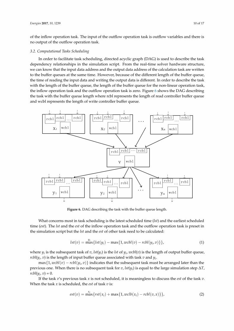
3.2. Computational Tasks Scheduling
In order to facilitate task scheduling, directed acyclic graph (DAG) is used to describe the taskdependency relationships in the simulation script. From the real-time solver hardware structure,we can know that the input data address and the output data address of the calculation task are writtento the buffer queues at the same time. However, because of the different length of the buffer queue,the time of reading the input data and writing the output data is different. In order to describe the taskwith the length of the buffer queue, the length of the buffer queue for the non-linear operation task,the inflow operation task and the outflow operation task is zero. Figure 6 shows the DAG describingthe task with the buffer queue length where rcbl represents the length of read controller buffer queueand wcbl represents the length of write controller buffer queue.
Energies 2017, 10, 1239 10 of 17
no input of the inflow operation task. The input of the outflow operation task is outflow variables and there is no output of the outflow operation task.
3.2. Computational Tasks Scheduling
In order to facilitate task scheduling, directed acyclic graph (DAG) is used to describe the task dependency relationships in the simulation script. From the real-time solver hardware structure, we can know that the input data address and the output data address of the calculation task are written to the buffer queues at the same time. However, because of the different length of the buffer queue, the time of reading the input data and writing the output data is different. In order to describe the task with the length of the buffer queue, the length of the buffer queue for the non-linear operation task, the inflow operation task and the outflow operation task is zero. Figure 6 shows the DAG describing the task with the buffer queue length where rcbl represents the length of read controller buffer queue and wcbl represents the length of write controller buffer queue.
...wcbl
rcblrcbl ...
y2
rcbl
wcbl
rcblrcbl
...
y1
rcbl
wcbl
rcblrcbl
...
ym
rcbl
...
wcbl
rcblrcbl
...
x2
rcbl
wcbl
rcblrcbl ...
x1
rcbl
wcbl
rcblrcbl
...
xm
rcbl
wcbl
rcblrcbl ...
v
rcbl
Figure 6. DAG describing the task with the buffer queue length.
What concerns most in task scheduling is the latest scheduled time (lst) and the earliest scheduled time (est). The lst and the est of the inflow operation task and the outflow operation task is preset in the simulation script but the lst and the est of other task need to be calculated:
( ) max{ ( ) max{1, ( ) ( , )}}iy
i ilst v lst y wcbl v rcbl y v= − − , (1)
where yi is the subsequent task of v, lst(yi) is the lst of yi, wcbl(v) is the length of output buffer queue, rcbl(yi, v) is the length of input buffer queue associated with task v and yi.
max{1, ( ) ( , )}iwcbl v rcbl y v− indicates that the subsequent task must be arranged later than the previous one. When there is no subsequent task for v, lst(yi) is equal to the large simulation step ΔT, rcbl(yi, v) = 0.
If the task v’s previous task x is not scheduled, it is meaningless to discuss the est of the task v. When the task x is scheduled, the est of task v is:
( ) max{ ( ) max{1, ( ) ( , )}}ix
i iest v rst x wclb x rcbl v x= + − , (2)
rpst(xi) is the scheduling time for task xi, wcbl(xi) is the length of output buffer queue, rcbb(v,xi) is the length of input buffer queue associated with task v and xi.
Figure 6. DAG describing the task with the buffer queue length.
What concerns most in task scheduling is the latest scheduled time (lst) and the earliest scheduledtime (est). The lst and the est of the inflow operation task and the outflow operation task is preset inthe simulation script but the lst and the est of other task need to be calculated:
lst(v) =yi
max{lst(yi)−max{1, wcbl(v)− rcbl(yi, v)}}, (1)
where yi is the subsequent task of v, lst(yi) is the lst of yi, wcbl(v) is the length of output buffer queue,rcbl(yi, v) is the length of input buffer queue associated with task v and yi.
max{1, wcbl(v)− rcbl(yi, v)} indicates that the subsequent task must be arranged later than theprevious one. When there is no subsequent task for v, lst(yi) is equal to the large simulation step ∆T,rcbl(yi, v) = 0.
If the task v’s previous task x is not scheduled, it is meaningless to discuss the est of the task v.When the task x is scheduled, the est of task v is:
est(v) =ximax{rst(xi) + max{1, wclb(xi)− rcbl(v, x)}}, (2)

Energies 2017, 10, 1239 11 of 17
rpst(xi) is the scheduling time for task xi, wcbl(xi) is the length of output buffer queue, rcbb(v,xi) isthe length of input buffer queue associated with task v and xi.
max{1, wclb(xi)− rcbl(v, xi)} also indicates that the subsequent task must be arranged later thanthe previous one. When there is no subsequent task for v, rst(v).
If the est of a task is less than or equal to the current execution time, the task is called a ready task.Although there are many PEs and a PE can take multiple tasks at the same time, we still cannot meetthe requirements of the ready task, that is, many ready tasks cannot be immediately scheduled. If thelst for a task is less than the current execution time, the simulation script cannot be finished in thespecified simulation step. Therefore, the strategy of prioritizing the lst is adopted in this article, that is,the earlier the lst, the sooner scheduled.
3.3. Data Scheduling
There are three concerns to consider during the scheduling tasks: (1) Whether the PE has inputand output ports and the selection lines to undertake the task; (2) Whether the input data is in thedata storage units or the data exchange stations which are associated with the inputs; (3) Whetherthe relevant data storage units can be read or written. When (2) and (3) cannot be met, the data canbe adjusted in advance to solve the problem, but such data scheduling may consume some data totransfer channel resources of the PEs directly. To arrange the tasks orderly, the three batches taskscheduling strategy is adopted. The first batch arranges the ready task which does not need to do datascheduling, the second batch arranges the ready task which meet the conditions (1,2) and the thirdbatch arranges the ready task that only satisfies the condition (1). Definitely, the ready task must lineup followed by the strategy of prioritizing the lst.
Data scheduling occurs within the microprocessor core during the second batch of the taskscheduling. There are three kinds of data scheduling methods: (1) Move the data directly to theappropriate data storage unit; (2) Arrange the data to the input of the PE in advance; (3) Copy the datato the appropriate data storage unit. Method (1) adjusts the data storage location and this will notconsume PE resources. If the adjusted data has been used in the scheduled task, it should be ensuredthat the change of data storage location will not cause the read/write conflicts of the scheduled data;Method (2) uses the data latch function of idle input port, the data arranged in advance may be justa part of the task inflow, et al. Method (3) achieves data adjustment through the data transmissionchannel, which will consume the data to transfer channel resources of the PEs directly. Therefore, thisarticle checks the feasibility of methods (1)−(3) one by one and puts the resource-saving strategy inthe first when there are multiple methods to schedule tasks. In the implementation of method (3),we gives priority to the microprocessor core internal resources rather than the data exchange stationstypically. Although the temporary data generated by method (3) can only be used once, we shouldkeep using it before being covered, avoiding unnecessary wastes.
Similarly, the above three kinds of data scheduling methods and the resource-saving prioritystrategy are still used in the third batch of the task scheduling. The data interactive ability of“hand-in-hand” is significantly higher than that of “data-pipeline”. Therefore, in the case of thesame resource consumption, we prefer the “hand-in-hand” data interaction. Since the data is storedin the microprocessor core after the execution of the task, the microprocessor core which has theminimum average distance between the migrated variable and the original variable will be givenpriority under the same conditions. The variable distance refers to the sum of the output buffer queuelengths experienced by the new variables generated from the two variables in the DAG.
Data scheduling is caused by the inaccurate data location and is closely related to the multi-valueparameters, circulation variables, inflow variables, outflow variables and other non-intermediatevariables. Since the data direct movement method can solve the problem of data storage inside themicroprocessor core. The non-intermediate variables initial storage scheme here focuses on whichmicroprocessor core is the non-intermediate variables assigned to. When a non-intermediate variableappears at multiple locations, only the earliest one is retained. The k-center point algorithm is used to

Energies 2017, 10, 1239 12 of 17
divide the non-intermediate variables of short variable distance into the same microprocessor core [16].Since the “hand-in” data interaction takes precedence over the “data-pipeline” data interaction,the non-intermediate variables is allocated following the principle of minimizing the distance ofnon-intermediate variables in adjacent PEs.
4. Micro-Grid Simulation Platform
4.1. The Construction of Simulation Platform
A Xilinx Virtex-7 VC709 FPGA (Xilinx, San Jose, CA, USA) was adopted as the developmentboard of the real-time solver, the FPGA chip of which is XC7VX690T-2FFG1761 with 693,120 logiccells, 108,300 configurable logic elements, 3600 DSP blocks and 147,036 KB of dual-port BRAMs.The real-time solver described in this article and [15] which can operate at 200 MHz and their resourceconsumptions are shown in Table 1 are constructed.
Table 1. FPGA resources utilized by two implementation methods.
Resource Type Configurable LogicBlock (CLB)
Storage Resource(Block RAM)
HardwareMultiplier (DSP)
Item ConsumptionNumber Utilization Consumption
Number Utilization ConsumptionNumber Utilization
Method inthis article 101,802 94% 1205.4 82% 2752 76%
Method in [15] 102,885 95% 1102.5 75% 1044 29%
As can be seen from Table 1, the method in this article can balance the FPGA resources. In additionto the real time solver, there are an industrial control machine, converter controllers and digital relayprotection devices. The industrial control machine is mainly used for micro-grid parameter changesand fault settings. The development board is inserted into the industrial control machine and thecommunication between the real time solver and the industrial control machine is carried out by PCIe.The sampled value (SV) message and the generic object oriented substation event (GOOSE) messagebetween the real time solver and the digital relay protection device are transmitted through the SFPinterface. The data exchange between the real time solver and the converter controller is accomplishedby inserting an I/O card into the industrial control machine.
As shown in Figure 7, a photovoltaic system, a photovoltaic-battery system and a micro-gasturbine system are arranged in the example of micro-grid. The photovoltaic array is simulated by acurrent generator, a backward diode, a shunt resistance and a series resistance. The universal modelequivalent circuit is selected for the battery, composed of internal resistance and controlled voltagesource connected in series. The micro-gas turbine adopts single shaft structure with high-frequencyalternating current (AC) at the motor outlet. The detailed parameters of other components of thelow-voltage micro-grid are described in [17].

Energies 2017, 10, 1239 13 of 17Energies 2017, 10, 1239 13 of 17
Figure 7. The low-voltage micro-grid example.
4.2. Performance test
Due to the lager simulation scale shown in Figure 7, the photovoltaic system, the photovoltaic-battery system and the micro-gas turbine system are replaced by the resistance-load in order to test the computing ability of the solver described in this article and [15]. The characteristic equation of the dynamic element in the system is differentiated by the trapezoid method, and the equivalent circuit of the electrical conductance and the historical current source in parallel is obtained. The simulation script describes how to calculate the self-admittance and the mutual admittance of each node, calculate the historical current source and the node injection current, solve the node voltage equation and get the branch voltage current. The simulation script is turned into orders by the order generator. We had it tested and the calculation time of the real time solver described in this article is 14.6 μs while the calculation time of the real time solver described in [15] is 20.44 μs, the reason for which is parallel computing ability of the real time solver in [15] is relatively low and the data interactions between microprocessor cores need to be specified in the form of computational tasks in the simulation script.
In order to verify the validity of the multi-valued parameter prestorage method, the simulation script eliminates the description of the self-admittance and the mutual admittance of each node, but establishes the influencing word and the guide word for them. There are 364 kinds of multi-valued parameter variables and the multi-value parameter of total is 2346. The calculation time of the real time solver described in this article is 10.8 μs by the multi-valued parameter prestorage, which reduces the original calculation time by 27%.
The simulation step of the photovoltaic system, the photovoltaic-battery system and the micro-gas turbine system in Figure 7 is set to 5 μs and that of the other part is set to 50 μs. The isolation transformer is described with the RL circuit in series and the explicit-implicit hybrid integration method is adopted [18]. In the simulation script, the fast time-varying influencing word, the slow time-varying influencing word, the non-linear influencing word and the guide word of the multi-valued parameter are established, and the inflow operation task and the outflow operation task with a time stamp are introduced. Since any microprocessor core in the real time solver will handle both the calculation of the 5 μs and 50 μs simulation step, it is not appropriate to describe the usage of real
Load 1
Load 3
Load 4
Load 6
Load 5
0.4kV
35kV
Photovoltaic-battery system Photovoltaic
system
Micro-gas turbine system
Load 2
PMSM
Figure 7. The low-voltage micro-grid example.
4.2. Performance test
Due to the lager simulation scale shown in Figure 7, the photovoltaic system, the photovoltaic-battery system and the micro-gas turbine system are replaced by the resistance-load in order to test thecomputing ability of the solver described in this article and [15]. The characteristic equation of thedynamic element in the system is differentiated by the trapezoid method, and the equivalent circuitof the electrical conductance and the historical current source in parallel is obtained. The simulationscript describes how to calculate the self-admittance and the mutual admittance of each node, calculatethe historical current source and the node injection current, solve the node voltage equation and getthe branch voltage current. The simulation script is turned into orders by the order generator. We hadit tested and the calculation time of the real time solver described in this article is 14.6 µs while thecalculation time of the real time solver described in [15] is 20.44 µs, the reason for which is parallelcomputing ability of the real time solver in [15] is relatively low and the data interactions betweenmicroprocessor cores need to be specified in the form of computational tasks in the simulation script.
In order to verify the validity of the multi-valued parameter prestorage method, the simulationscript eliminates the description of the self-admittance and the mutual admittance of each node,but establishes the influencing word and the guide word for them. There are 364 kinds of multi-valuedparameter variables and the multi-value parameter of total is 2346. The calculation time of the realtime solver described in this article is 10.8 µs by the multi-valued parameter prestorage, which reducesthe original calculation time by 27%.
The simulation step of the photovoltaic system, the photovoltaic-battery system and the micro-gasturbine system in Figure 7 is set to 5 µs and that of the other part is set to 50 µs. The isolationtransformer is described with the RL circuit in series and the explicit-implicit hybrid integration methodis adopted [18]. In the simulation script, the fast time-varying influencing word, the slow time-varyinginfluencing word, the non-linear influencing word and the guide word of the multi-valued parameterare established, and the inflow operation task and the outflow operation task with a time stamp areintroduced. Since any microprocessor core in the real time solver will handle both the calculationof the 5 µs and 50 µs simulation step, it is not appropriate to describe the usage of real time solver

Energies 2017, 10, 1239 14 of 17
with the execution time of the last task. We use the sum of the idle time of the 5 µs simulation step todescribe the usage of the microprocessor cores. Table 2 shows the usage of eight microprocessor coresin the situation of micro-grid real-time simulation in Figure 7.
Table 2. The usage of eight microprocessor cores.
Microprocessor Core Label 1 2 3 4 5 6 7 8
The idle time 8.24 µs 8.78 µs 8.13 µs 8.67 µs 8.11 µs 8.93 µs 8.31 µs 8.25 µs
It can be seen from Table 2 that the use of the microprocessor core is reasonable, there is nocentralized use of some microprocessor cores and there is no idle phenomenon of some microprocessorcores. Therefore, it can be expected that there is at least 8 µs can be used to expand the simulation scale.
In order to verify the correctness of the orders, the simulation model with the same parameters asthe real time solver is built on power systems computer aided design (PSCAD) and the simulation stepis 5 µs. While the micro-grid operates stably, a three-phase ground short-circuit fault is set in the node8, and the fault is removed after 0.1 s. The three-phase voltage waveform of node 8, the three-phaseoutput voltage waveform of node 37, the A phase output current waveform of node 30 and the inverterDC voltage waveform of node 32 are shown as Figures 8–11.
Energies 2017, 10, 1239 14 of 17
time solver with the execution time of the last task. We use the sum of the idle time of the 5 μs simulation step to describe the usage of the microprocessor cores. Table 2 shows the usage of eight microprocessor cores in the situation of micro-grid real-time simulation in Figure 7.
Table 2. The usage of eight microprocessor cores.
Microprocessor Core Label 1 2 3 4 5 6 7 8The idle time 8.24 μs 8.78 μs 8.13 μs 8.67 μs 8.11 μs 8.93 μs 8.31 μs 8.25 μs
It can be seen from Table 2 that the use of the microprocessor core is reasonable, there is no centralized use of some microprocessor cores and there is no idle phenomenon of some microprocessor cores. Therefore, it can be expected that there is at least 8 μs can be used to expand the simulation scale.
In order to verify the correctness of the orders, the simulation model with the same parameters as the real time solver is built on power systems computer aided design (PSCAD) and the simulation step is 5 μs. While the micro-grid operates stably, a three-phase ground short-circuit fault is set in the node 8, and the fault is removed after 0.1 s. The three-phase voltage waveform of node 8, the three-phase output voltage waveform of node 37, the A phase output current waveform of node 30 and the inverter DC voltage waveform of node 32 are shown as Figures 8–11.
Figure 8. The three-phase voltage waveform of node 8.
Figure 9. The three-phase output voltage waveform of node 37.
U[V
]
t[s]
U[V
]
t[s]
Figure 8. The three-phase voltage waveform of node 8.
Energies 2017, 10, 1239 14 of 17
time solver with the execution time of the last task. We use the sum of the idle time of the 5 μs simulation step to describe the usage of the microprocessor cores. Table 2 shows the usage of eight microprocessor cores in the situation of micro-grid real-time simulation in Figure 7.
Table 2. The usage of eight microprocessor cores.
Microprocessor Core Label 1 2 3 4 5 6 7 8The idle time 8.24 μs 8.78 μs 8.13 μs 8.67 μs 8.11 μs 8.93 μs 8.31 μs 8.25 μs
It can be seen from Table 2 that the use of the microprocessor core is reasonable, there is no centralized use of some microprocessor cores and there is no idle phenomenon of some microprocessor cores. Therefore, it can be expected that there is at least 8 μs can be used to expand the simulation scale.
In order to verify the correctness of the orders, the simulation model with the same parameters as the real time solver is built on power systems computer aided design (PSCAD) and the simulation step is 5 μs. While the micro-grid operates stably, a three-phase ground short-circuit fault is set in the node 8, and the fault is removed after 0.1 s. The three-phase voltage waveform of node 8, the three-phase output voltage waveform of node 37, the A phase output current waveform of node 30 and the inverter DC voltage waveform of node 32 are shown as Figures 8–11.
Figure 8. The three-phase voltage waveform of node 8.
Figure 9. The three-phase output voltage waveform of node 37.
U[V
]
t[s]
U[V
]
t[s]
Figure 9. The three-phase output voltage waveform of node 37.

Energies 2017, 10, 1239 15 of 17Energies 2017, 10, 1239 15 of 17
Figure 10. The A phase output current waveform of node 30.
Figure 11. The inverter DC voltage waveform of node 32.
Figures 8–11 are partially enlarged and then we can be seen from the enlarged figure that the error between the actual simulation waveform and PSCAD simulation waveform is within 5%, the method in this article has certain simulation accuracy. The main reason for the error is: In FPGA, the simulation step of AC/DC, AC/AC, DC/DC converter is set to 5 μs and the other part is set to 50 μs while PSCAD uses a 5 μs simulation step for the whole system.
5. Conclusions
(1) Reuse modules are utilized to build the arithmetic expression circuits and the comparison expression circuits. The input ports of PEs are shared by arithmetic expression circuits, comparison expression circuits, function circuits and data transmission channels, which effectively reduces the number of PE ports and their demand for resources.
(2) The relationship between the influencing word and the multi-valued parameter is defined. The conversion of guide word address to the current value address is integrated into the processing procedure of order by using the influencing word and the decoding method, which effectively reduces the workload of the PEs.
(3) The data inflow/outflow Ping-Pong circuits of various rhythms and the inflow/outflow operation tasks with time stamps are built. The improved DAG is used to describe the
U[V
]
t[s]
U[V
]
t[s]
Figure 10. The A phase output current waveform of node 30.
Energies 2017, 10, 1239 15 of 17
Figure 10. The A phase output current waveform of node 30.
Figure 11. The inverter DC voltage waveform of node 32.
Figures 8–11 are partially enlarged and then we can be seen from the enlarged figure that the error between the actual simulation waveform and PSCAD simulation waveform is within 5%, the method in this article has certain simulation accuracy. The main reason for the error is: In FPGA, the simulation step of AC/DC, AC/AC, DC/DC converter is set to 5 μs and the other part is set to 50 μs while PSCAD uses a 5 μs simulation step for the whole system.
5. Conclusions
(1) Reuse modules are utilized to build the arithmetic expression circuits and the comparison expression circuits. The input ports of PEs are shared by arithmetic expression circuits, comparison expression circuits, function circuits and data transmission channels, which effectively reduces the number of PE ports and their demand for resources.
(2) The relationship between the influencing word and the multi-valued parameter is defined. The conversion of guide word address to the current value address is integrated into the processing procedure of order by using the influencing word and the decoding method, which effectively reduces the workload of the PEs.
(3) The data inflow/outflow Ping-Pong circuits of various rhythms and the inflow/outflow operation tasks with time stamps are built. The improved DAG is used to describe the
U[V
]
t[s]
U[V
]
t[s]
Figure 11. The inverter DC voltage waveform of node 32.
Figures 8–11 are partially enlarged and then we can be seen from the enlarged figure that theerror between the actual simulation waveform and PSCAD simulation waveform is within 5%, themethod in this article has certain simulation accuracy. The main reason for the error is: In FPGA,the simulation step of AC/DC, AC/AC, DC/DC converter is set to 5 µs and the other part is set to50 µs while PSCAD uses a 5 µs simulation step for the whole system.
5. Conclusions
(1) Reuse modules are utilized to build the arithmetic expression circuits and the comparisonexpression circuits. The input ports of PEs are shared by arithmetic expression circuits,comparison expression circuits, function circuits and data transmission channels, which effectivelyreduces the number of PE ports and their demand for resources.
(2) The relationship between the influencing word and the multi-valued parameter is defined.The conversion of guide word address to the current value address is integrated into theprocessing procedure of order by using the influencing word and the decoding method, whicheffectively reduces the workload of the PEs.

Energies 2017, 10, 1239 16 of 17
(3) The data inflow/outflow Ping-Pong circuits of various rhythms and the inflow/outflow operationtasks with time stamps are built. The improved DAG is used to describe the relationshipbetween multi-rate simulation tasks, which makes it possible to realize the overall arrangementof multi-rate simulation task.
(4) The k-center point algorithm is used to initialize the allocation of the non-intermediate variablesto the microprocessor cores. The data scheduling is carried out following the principle of savingthe resources and minimizing the average distance between variables, which makes the ordergenerator has the ability of auto scheduling.
Acknowledgments: The work presented was supported by the National Natural Science Foundation of China(No. 51477114).
Author Contributions: Bingda Zhang put forward the research direction, organized the research activities,provided theory guidance, and completed the revision of the article. Shaowen Fu completed the principle analysisand the method design, performed the simulation, drafted the article. Zhao Jin and Ruizhao Hu analyzed thesimulation results. Valuable comments on the first draft were received from Bingda Zhang. All four were involvedin revising the article.
Conflicts of Interest: The authors declare no conflict of interest.
References
1. Jeon, J.H.; Kim, J.Y.; Kim, H.M.; Kim, S.K.; Cho, C.; Kim, J.M.; Ahn, J.B.; Nam, K.Y. Development of Hardwarein-the-Loop Simulation System for Testing Operation and Control Functions of Microgrid. IEEE Trans.Power Electron. 2010, 25, 2919–2929. [CrossRef]
2. Matar, M.; Karimi, H.; Etemadi, A.; Iravani, R. A High Performance Real-time Simulator for ControllersHardware-in-the-Loop Testing. Energies 2012, 5, 1713–1733. [CrossRef]
3. Yan, B.; Wang, B.; Zhu, L.; Liu, H.; Liu, Y.; Ji, X.; Liu, D. A Novel, Stable, and Economic Power SharingScheme for an Autonomous Microgrid in the Energy Internet. Energies 2015, 8, 12741–12764. [CrossRef]
4. Chen, Y.; Dinavahi, V. FPGA-based Real-time EMTP. IEEE Trans. Power Deliv. 2009, 24, 892–902. [CrossRef]5. Kai, S.; Carlson, E. Nested Fast and Simultaneous Solution for Time-domain Simulation of Integrative
Power-Electric and Electronic Systems. IEEE Trans. Power Deliv. 2006, 22, 277–287.6. Wang, X.; Zhang, B.; Chen, X. Implementation of Fine Granularity Parallelization in Power System Real-time
Simulation. J. Tianjin Univ. 2016, 49, 513–519.7. Benigni, A.; Monti, A.; Dougal, R.A. Latency-based Approach to the Simulation of Large Power Electronics
Systems. IEEE Trans. Power Electron. 2014, 29, 3201–3213. [CrossRef]8. Qi, L.; Langston, J.; Steurer, M.; Sundaram, A. Implementation and Validation of a Five-Level STATCOM
Model in the RTDS Small Time-Step Environment. In Proceedings of the IEEE Power and Energy SocietyGeneral Meeting (PES’09), Calgary, AB, Canada, 26–30 July 2009.
9. Dufour, C.; Abourida, S.; Belanger, J. Hardware-in-the-Loop Simulation of Power Drives with RT-LAB.In Proceedings of the International Conference on Power Electronics and Drives Systems, Kuala Lumpur,Malaysia, 28 November–1 December 2005.
10. Ou, K.J.; Maguire, T.; Warkentin, B. Research and Application of Small Time-Step Simulation for MMCVSC-HVDC in RTDS. In Proceedings of the International Conference on Power System Technology, Chengdu,China, 20–22 October 2014.
11. Liu, J.; Dinavahi, V. A Real-time Nonlinear Hysteretic Power Transformer Transient Model on FPGA.IEEE Trans. Ind. Electron. 2014, 61, 3587–3597. [CrossRef]
12. Wang, C.; Ding, C.; Li, P.; Yu, H. Real-time Transient Simulation for Distribution Systems based on FPGA,Part I: Module realization. Proc. CSEE 2014, 34, 161–167.
13. Wang, C.; Ding, C.; Li, P.; Yu, H. Real-time Transient Simulation for Distribution Systems based on FPGA,Part II: System Architecture and Algorithm Verification. Proc. CSEE 2014, 34, 628–634.
14. Chen, Y.; Dinavahi, V. Multi-FPGA Digital Hardware Design for Detailed Large-scale Real-timeElectromagnetic Transient Simulation of Power Systems. IET Gener. Transm. Distrib. 2013, 7, 451–463.[CrossRef]
15. Zhang, B.; Wang, L. Real-time Simulation Training System for Substation based on FPGA. Power Syst.Prot. Control 2017, 45, 55–61.

Energies 2017, 10, 1239 17 of 17
16. Sung, T.; Kong, L.; Tsai, P. A Distance Coefficient-based Algorithm for K-center Selection in Wireless SensorNetworks. In Proceedings of the 2017 IEEE International Conference on Consumer Electronics, Taipei,Taiwan, 12–14 June 2017.
17. Papathanassiou, S.; Hatziargyriou, N.; Strunz, K. A Benchmark Low Voltage Microgrid Network.In Proceedings of the CIGRE Symposium Power System and Dispersed Generation, Athens, Greece,13–16 April 2005.
18. Toshiji, K.; Kaoru, I.; Takayuki, F. Multirate Analysis Method for a Power Electronic System by CircuitPartitioning. IEEE Trans. Power Electron. 2009, 24, 2791–2802.
© 2017 by the authors. Licensee MDPI, Basel, Switzerland. This article is an open accessarticle distributed under the terms and conditions of the Creative Commons Attribution(CC BY) license (http://creativecommons.org/licenses/by/4.0/).