fpga 03-cpld-and-fpga
TRANSCRIPT
ENGR. RASHID FARID CHISHTILECTURER,DEE, FET, IIUI
WEEK 3
CPLD AND FPGA
FPGA Based System Design
Saturday, April 15, 2023
1
www.iiu.edu.pk
PAL-likeblock
I/O
blo
ck
PAL-likeblock
I/O b
lock
PAL-likeblock
I/O
blo
ck
PAL-likeblock
I/O b
lock
Interconnection wires
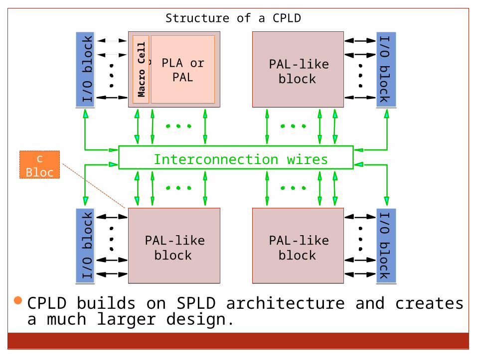
Structure of a CPLD
Logic
Block
CPLD builds on SPLD architecture and creates a much larger design.
Macro
Cell
Macro
Cell
PLA or PAL
PLA or PAL
CPLD can be used to integrate the functions of a number of SPLDs into a single device.
The CPLD consists of a number of logic blocks (sometimes referred to as functional blocks), each of which contains a macrocell and either a PLA or PAL circuit arrangement.
In the center of the design is a global programmable interconnect. This interconnect allows connections to the logic block macrocells and the I/O cell arrays (the digital I/O cells of the CPLD connecting to the pins of the CPLD package).
CPLDs utilize nonvolatile memory such as EPROM, EEPROM, and flash memory
CPLD
Saturday, April 15, 2023
3
www.iiu.edu.pk
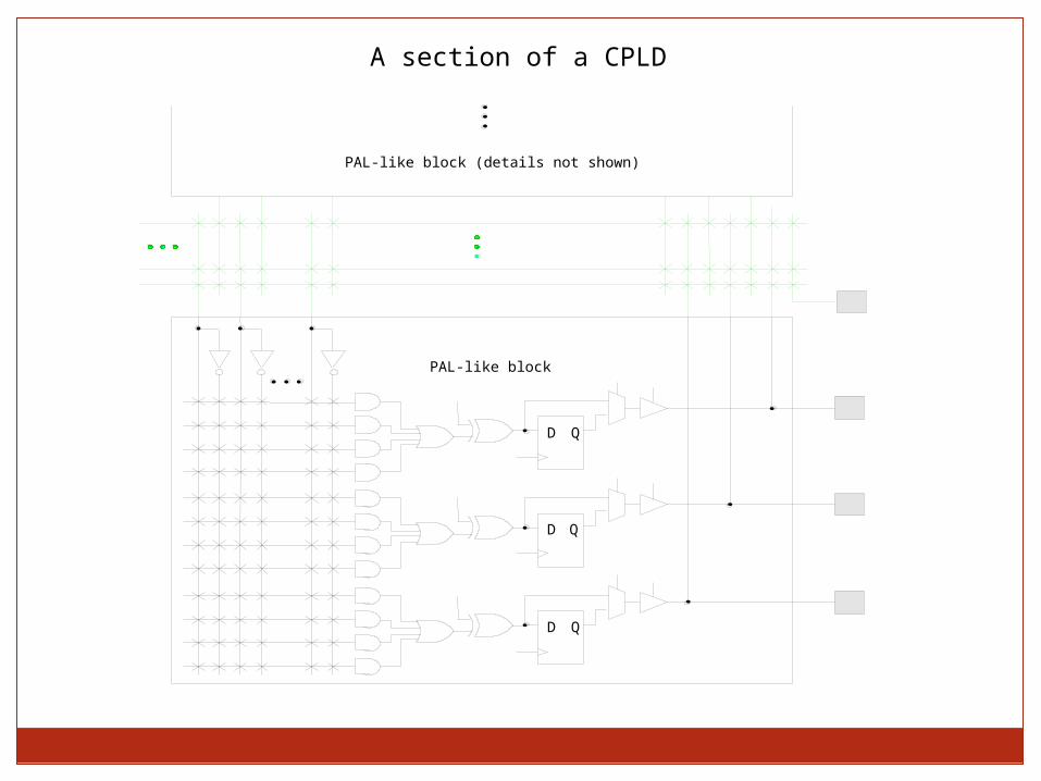
A section of a CPLD
D Q
D Q
D Q
PAL-like block (details not shown)
PAL-like block
Saturday, April 15, 2023
5
www.iiu.edu.pk
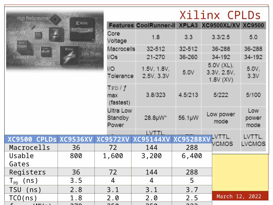
XC9500 CPLDs XC9536XV XC9572XV XC95144XV XC95288XVMacrocells 36 72 144 288Usable Gates 800 1,600 3,200 6,400Registers 36 72 144 288TPD (ns) 3.5 4 4 5TSU (ns) 2.8 3.1 3.1 3.7TCO(ns) 1.8 2.0 2.0 2.5fSYSTEM (MHz) 278 250 250 222
Xilinx CPLDs
Xilinx CPLDs
Saturday, April 15, 2023www.iiu.edu.pk
Saturday, April 15, 2023
7
www.iiu.edu.pk
Xilinx XC9500 CPLD
Saturday, April 15, 2023
8
www.iiu.edu.pk
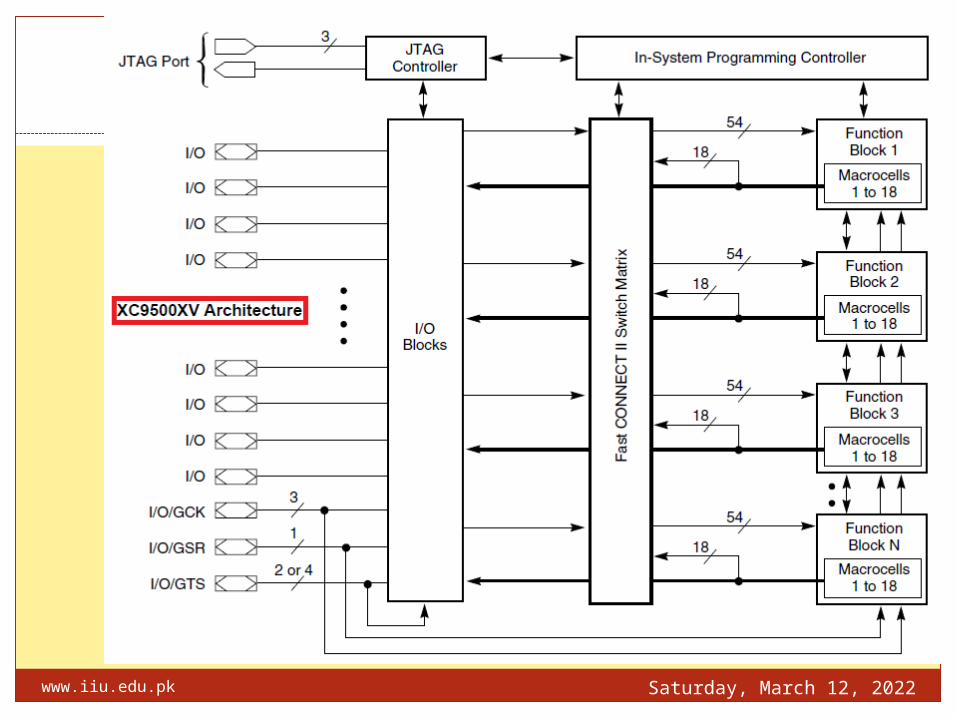
The Xilinx XC9500 family of CPLDs are flash-based (EEPROM) and in-system programmable.
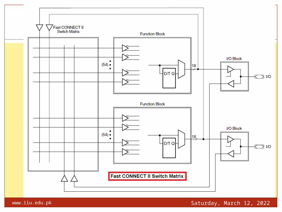
The devices are organized as an array of functional blocks in a PAL-like structure with wide AND gates and fast flip-flops.
Each function block contains up to 18 independent macrocells (see Figure 8-49), and can accommodate 54 inputs and drive 18 outputs (depending on the packaging).
A FastCONNECT switch-matrix technology ensures that an application can be fully routed even when the device utilization is high.
I/O blocks (IOBs) buffer the inputs and outputs to the device and also receive the global clock and S-R signals.
The output buffers have a programmable slew rate.
The Xilinx XC9500 family of CPLDs are flash-based (EEPROM) and in-system programmable.
The devices are organized as an array of functional blocks in a PAL-like structure with wide AND gates and fast flip-flops.
Each function block contains up to 18 independent macrocells (see Figure 8-49), and can accommodate 54 inputs and drive 18 outputs (depending on the packaging).
A FastCONNECT switch-matrix technology ensures that an application can be fully routed even when the device utilization is high.
I/O blocks (IOBs) buffer the inputs and outputs to the device and also receive the global clock and S-R signals.
The output buffers have a programmable slew rate.
Saturday, April 15, 2023
9
www.iiu.edu.pk
Saturday, April 15, 2023
10
www.iiu.edu.pk
Saturday, April 15, 2023
11
www.iiu.edu.pk
Saturday, April 15, 2023
12
www.iiu.edu.pk
Xilinx XC9500 CPLD
Saturday, April 15, 2023
13
www.iiu.edu.pk
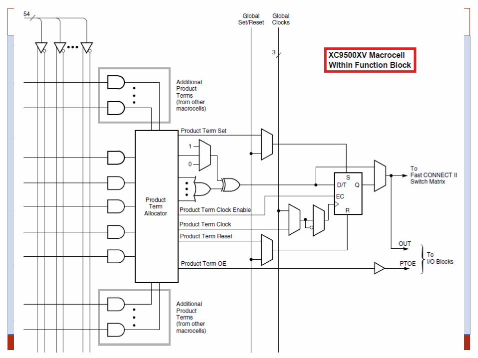
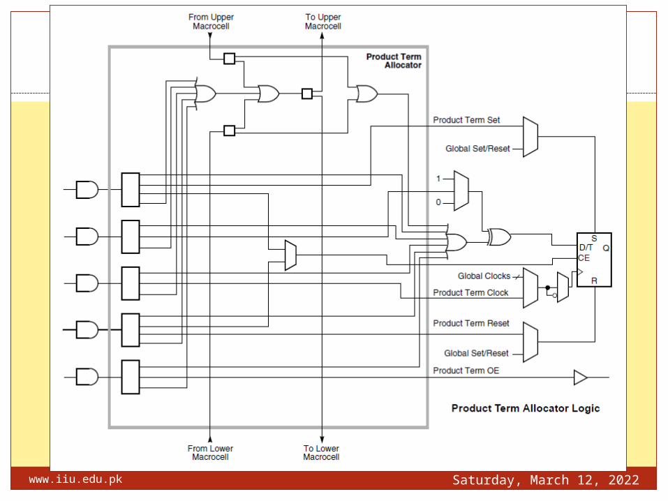
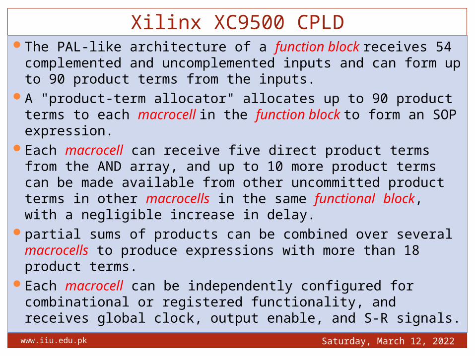
The PAL-like architecture of a function block receives 54 complemented and uncomplemented inputs and can form up to 90 product terms from the inputs.
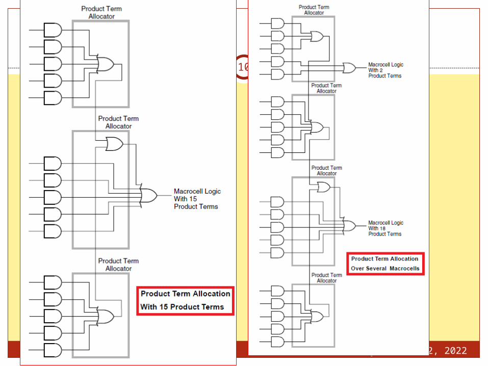
A "product-term allocator" allocates up to 90 product terms to each macrocell in the function block to form an SOP expression.
Each macrocell can receive five direct product terms from the AND array, and up to 10 more product terms can be made available from other uncommitted product terms in other macrocells in the same functional block, with a negligible increase in delay.
partial sums of products can be combined over several macrocells to produce expressions with more than 18 product terms.
Each macrocell can be independently configured for combinational or registered functionality, and receives global clock, output enable, and S-R signals.
The PAL-like architecture of a function block receives 54 complemented and uncomplemented inputs and can form up to 90 product terms from the inputs.
A "product-term allocator" allocates up to 90 product terms to each macrocell in the function block to form an SOP expression.
Each macrocell can receive five direct product terms from the AND array, and up to 10 more product terms can be made available from other uncommitted product terms in other macrocells in the same functional block, with a negligible increase in delay.
partial sums of products can be combined over several macrocells to produce expressions with more than 18 product terms.
Each macrocell can be independently configured for combinational or registered functionality, and receives global clock, output enable, and S-R signals.
Xilinx XC9500 CPLD
Saturday, April 15, 2023
14
www.iiu.edu.pk
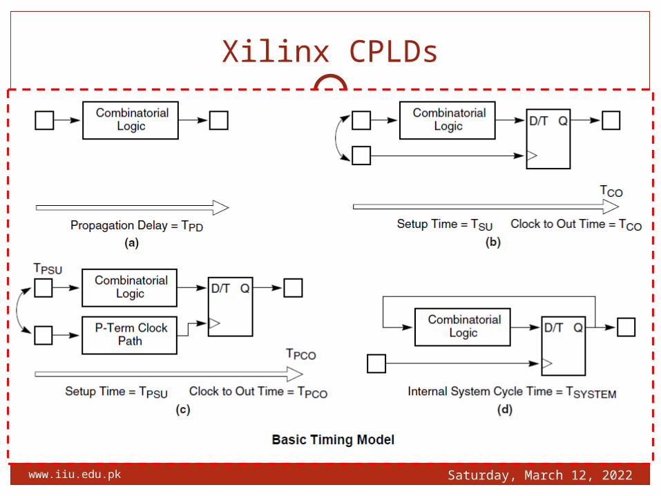
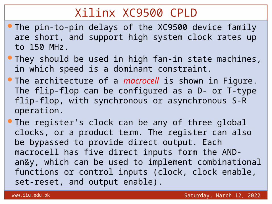
The pin-to-pin delays of the XC9500 device family are short, and support high system clock rates up to 150 MHz.
They should be used in high fan-in state machines, in which speed is a dominant constraint.
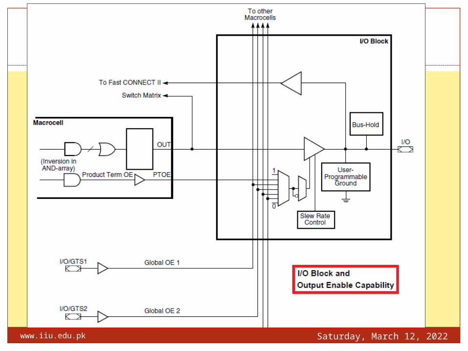
The architecture of a macrocell is shown in Figure. The flip-flop can be configured as a D- or T-type flip-flop, with synchronous or asynchronous S-R operation.
The register's clock can be any of three global clocks, or a product term. The register can also be bypassed to provide direct output. Each macrocell has five direct inputs form the AND-an&y, which can be used to implement combinational functions or control inputs (clock, clock enable, set-reset, and output enable).
The pin-to-pin delays of the XC9500 device family are short, and support high system clock rates up to 150 MHz.
They should be used in high fan-in state machines, in which speed is a dominant constraint.
The architecture of a macrocell is shown in Figure. The flip-flop can be configured as a D- or T-type flip-flop, with synchronous or asynchronous S-R operation.
The register's clock can be any of three global clocks, or a product term. The register can also be bypassed to provide direct output. Each macrocell has five direct inputs form the AND-an&y, which can be used to implement combinational functions or control inputs (clock, clock enable, set-reset, and output enable).
Saturday, April 15, 2023www.iiu.edu.pk
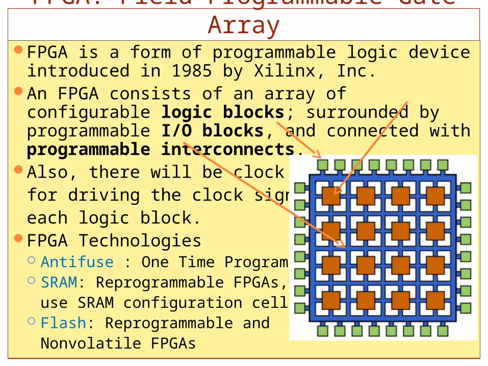
15FPGA is a form of programmable logic device introduced in
1985 by Xilinx, Inc.An FPGA consists of an array of configurable logic blocks;
surrounded by programmable I/O blocks, and connected with programmable interconnects.
Also, there will be clock circuitryfor driving the clock signals to each logic block.
FPGA Technologies Antifuse : One Time Programmable SRAM: Reprogrammable FPGAs,
use SRAM configuration cell Flash: Reprogrammable and
Nonvolatile FPGAs
FPGA is a form of programmable logic device introduced in 1985 by Xilinx, Inc.
An FPGA consists of an array of configurable logic blocks; surrounded by programmable I/O blocks, and connected with programmable interconnects.
Also, there will be clock circuitryfor driving the clock signals to each logic block.
FPGA Technologies Antifuse : One Time Programmable SRAM: Reprogrammable FPGAs,
use SRAM configuration cell Flash: Reprogrammable and
Nonvolatile FPGAs
FPGA: Field Programmable Gate Array
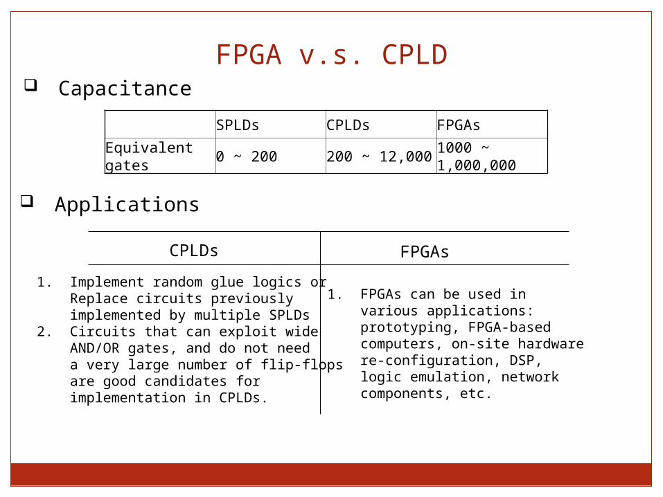
FPGA v.s. CPLD Capacitance
SPLDs CPLDs FPGAs
Equivalent gates 0 ~ 200 200 ~ 12,000 1000 ~ 1,000,000
Applications
CPLDs FPGAs
1. Implement random glue logics or Replace circuits previously implemented by multiple SPLDs
2. Circuits that can exploit wide AND/OR gates, and do not need a very large number of flip-flops are good candidates for implementation in CPLDs.
1. FPGAs can be used in various applications: prototyping, FPGA-based computers, on-site hardware re-configuration, DSP, logic emulation, network components, etc.
Saturday, April 15, 2023www.iiu.edu.pk
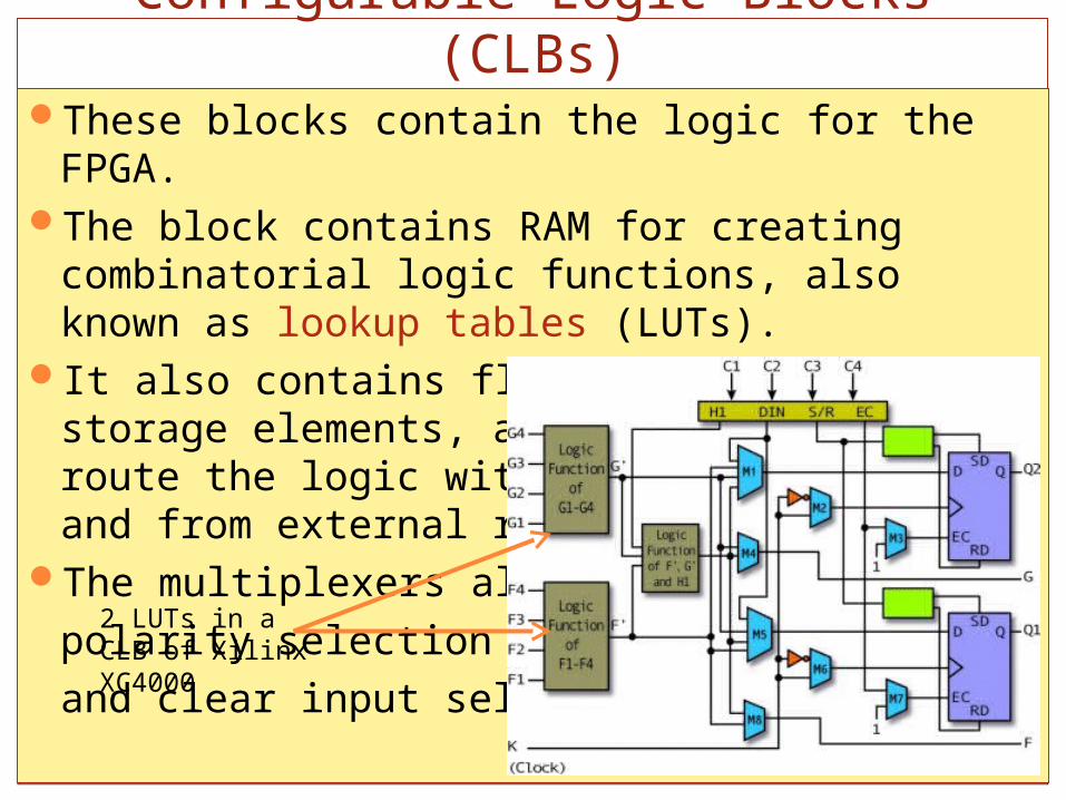
17These blocks contain the logic for the FPGA.The block contains RAM for creating combinatorial logic
functions, also known as lookup tables (LUTs). It also contains flip-flops for clocked storage elements, and
multiplexers to route the logic within the block and to and from external resources.
The multiplexers also allow
polarity selection and reset
and clear input selection.
These blocks contain the logic for the FPGA.The block contains RAM for creating combinatorial logic
functions, also known as lookup tables (LUTs). It also contains flip-flops for clocked storage elements, and
multiplexers to route the logic within the block and to and from external resources.
The multiplexers also allow
polarity selection and reset
and clear input selection.
Configurable Logic Blocks (CLBs)
2 LUTs in a CLB of Xilinx XC4000
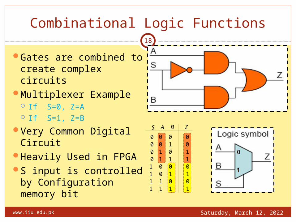
Gates are combined to create complex circuits
Multiplexer Example If S=0, Z=A If S=1, Z=B
Very Common Digital Circuit
Heavily Used in FPGAS input is controlled by
Configuration memory bit
Combinational Logic Functions
Saturday, April 15, 2023
18
www.iiu.edu.pk
0 0 1 1
1 0 1
ZA
0
B
0000
S
011
0
0 0 1 1
1 0 1
0 1 1 1 1
101
0
Saturday, April 15, 2023www.iiu.edu.pk 19
0
0
1
1
0
1
0
1
1
0
0
1
x 1
x 2
(b) f 1
x 1
x 2
x 1
x 2
+ =
f 1
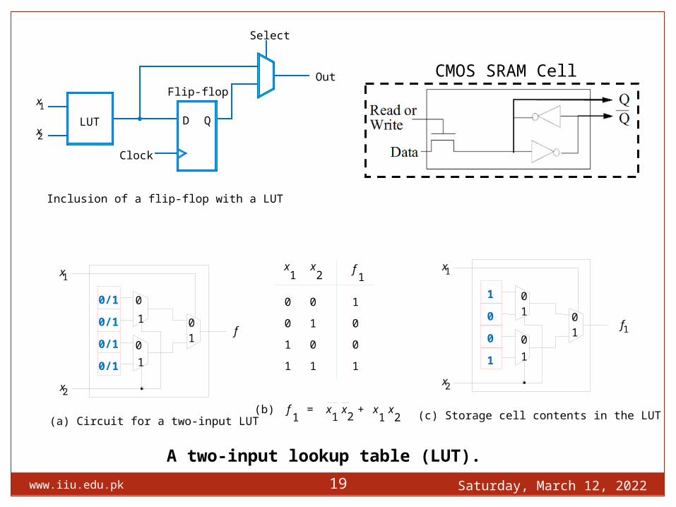
A two-input lookup table (LUT).
(c) Storage cell contents in the LUT
x 1
x 2
1
0
0
1
f 1
1
1
0
0 1 0
(a) Circuit for a two-input LUT
x 1
x 2
f
0/1
0/1
0/1
0/1
1
1
0
0 1 0
Out
D Q
Clock
Select
Flip-flop
LUT
Inclusion of a flip-flop with a LUT
x 1
x 2
CMOS SRAM Cell
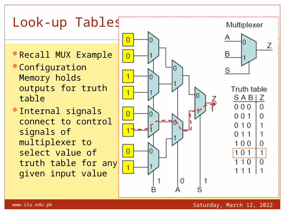
Recall MUX ExampleConfiguration
Memory holds outputs for truth table
Internal signals connect to control signals of multiplexer to select value of truth table for any given input value
Look-up Tables
Saturday, April 15, 2023
20
www.iiu.edu.pk
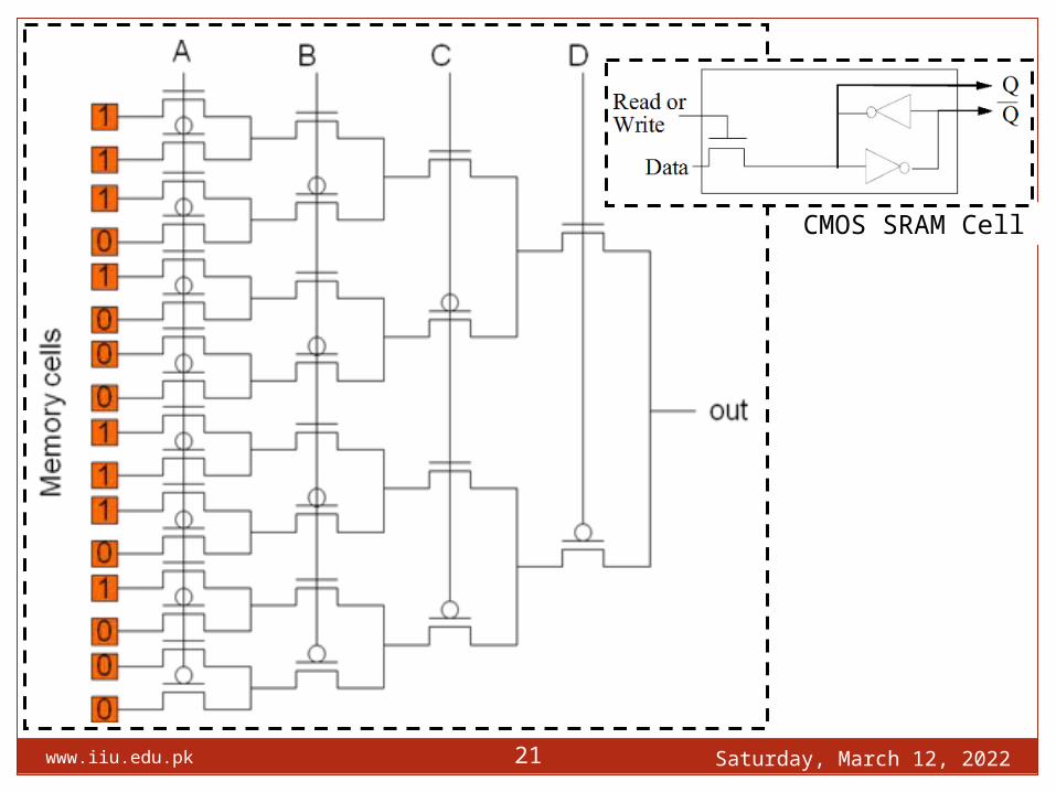
Saturday, April 15, 2023www.iiu.edu.pk 21
CMOS SRAM Cell
Saturday, April 15, 2023www.iiu.edu.pk 22
Saturday, April 15, 2023www.iiu.edu.pk 23
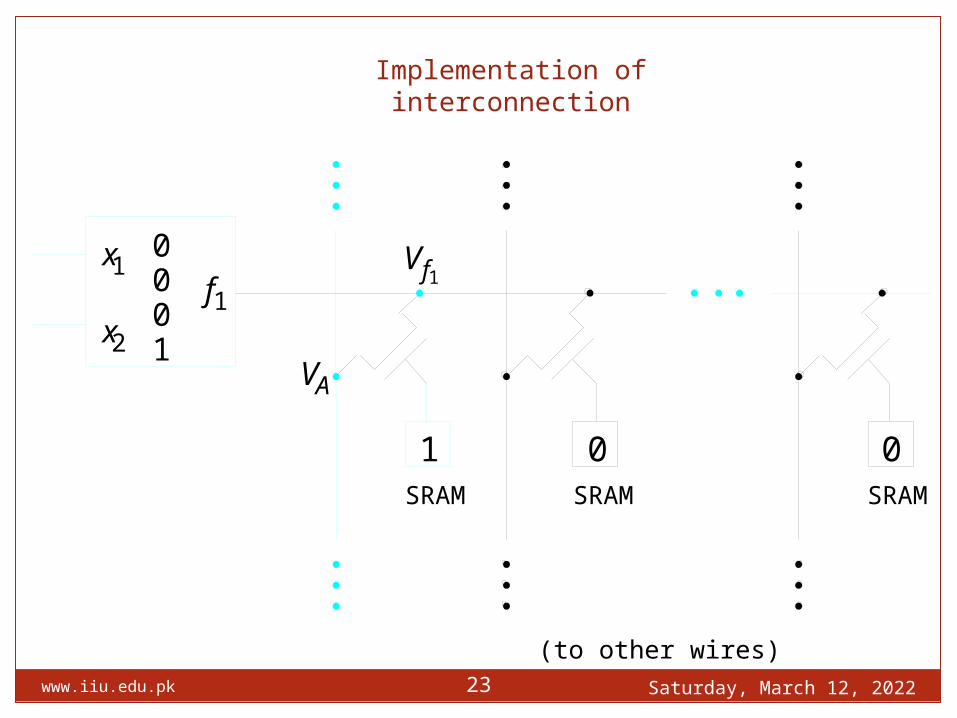
Implementation of interconnection
1 0
V f 1
V A
0
0 0 0 1
x 1
x 2
f 1
SRAM SRAM SRAM
(to other wires)
Saturday, April 15, 2023
24
www.iiu.edu.pk
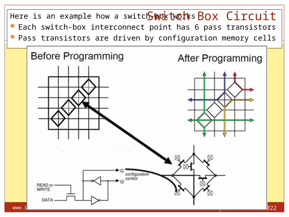
Here is an example how a switch-box works Each switch-box interconnect point has 6 pass transistors Pass transistors are driven by configuration memory cells
Switch Box Circuit
Programmable Interconnect
Saturday, April 15, 2023
25
www.iiu.edu.pk
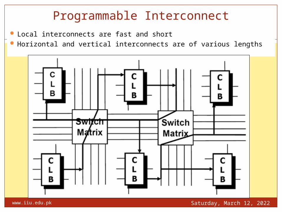
Local interconnects are fast and short Horizontal and vertical interconnects are of various lengths
Saturday, April 15, 2023www.iiu.edu.pk
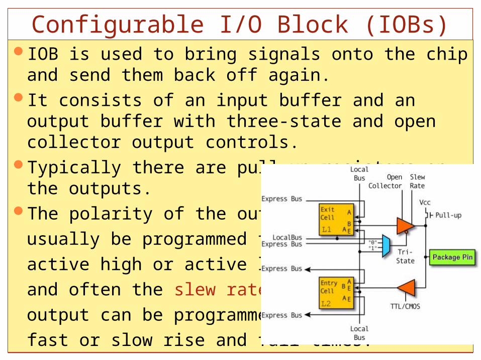
26IOB is used to bring signals onto the chip and send them
back off again.It consists of an input buffer and an output buffer with three-
state and open collector output controls. Typically there are pull up resistors on the outputs. The polarity of the output can
usually be programmed for
active high or active low output,
and often the slew rate of the
output can be programmed for
fast or slow rise and fall times.
IOB is used to bring signals onto the chip and send them back off again.
It consists of an input buffer and an output buffer with three-state and open collector output controls.
Typically there are pull up resistors on the outputs. The polarity of the output can
usually be programmed for
active high or active low output,
and often the slew rate of the
output can be programmed for
fast or slow rise and fall times.
Configurable I/O Block (IOBs)