a low noise preamplifier with improved output reflec tion for … homepage/2m preamp with low... ·...
TRANSCRIPT
A Low Noise Preamplifier With Improved Output Reflection For The 2m Band
By Gunthard Kraus, DG8GB
First published in the German UKW Berichte journal issue 4/2013
The development of LNAs for the frequency range from 1 to 1.7GHz was presented in a lecture atthe UKW Conference 2012 in Bensheim, it was subsequently published in [1]. Due to the excellentnoise characteristics of the prototype a version for the 70cm band was examined, this gave similargood results as described in [2]. A 145MHz version has also been tested and the results werepresented at the UKW conference 2013. The problems that occurred and the solutions found aredescribed in the following text.
1 Introduction
Following the good experience with 1 to 1.7GHz it suggested that development should be focussedon the lower bands. The MM1C properties show that it is for use in the area of 1.9GHz but the noiseproperties are not documented at lower frequencies. The development for a 70cm amplifier waspublished in VHF Communications Magazine [2] with the data obtained. It showed that theminimum noise figure was virtually constant at NF 0.3 - 0.4dB even with the reduction in frequency.These results motivated the development of a version of the LNA for the 2m band in the expectationthat such values would be measured there as well. There was the following wish list:
Noise figure: maximum 0.4dB
(S21) of at least 20dB
Absolute stability (k greater than 1 up to 10GHz)
The output reflection S22 that should be possible (Dream value = -20dB at 145MHz)
Part 1: The development
changes
1.1. The amplifier changes
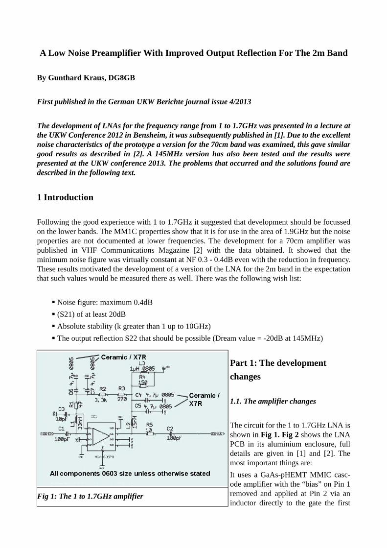
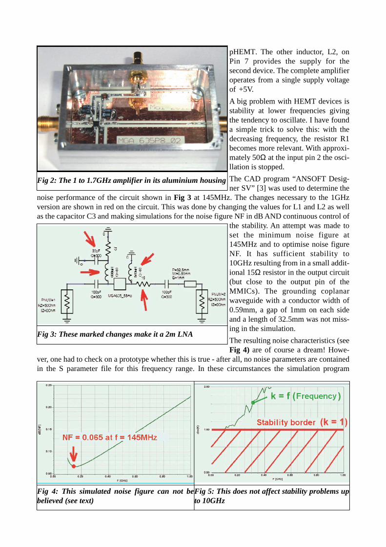
The circuit for the 1 to 1.7GHz LNA isshown in Fig 1. Fig 2 shows the LNAPCB in its aluminium enclosure, fulldetails are given in [1] and [2]. Themost important things are:
It uses a GaAs-pHEMT MMIC casc-ode amplifier with the “bias” on Pin 1removed and applied at Pin 2 via aninductor directly to the gate the first
Fig 1: The 1 to 1.7GHz amplifier
pHEMT. The other inductor, L2, onPin 7 provides the supply for thesecond device. The complete amplifieroperates from a single supply voltageof +5V.
A big problem with HEMT devices isstability at lower frequencies givingthe tendency to oscillate. I have founda simple trick to solve this: with thedecreasing frequency, the resistor R1becomes more relevant. With approxi-mately 50Ω at the input pin 2 the osci-llation is stopped.
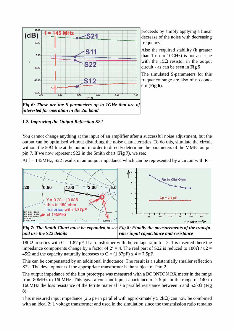
The CAD program “ANSOFT Desig-ner SV” [3] was used to determine the
noise performance of the circuit shown in Fig 3 at 145MHz. The changes necessary to the 1GHzversion are shown in red on the circuit. This was done by changing the values for L1 and L2 as wellas the capacitor C3 and making simulations for the noise figure NF in dB AND continuous control of
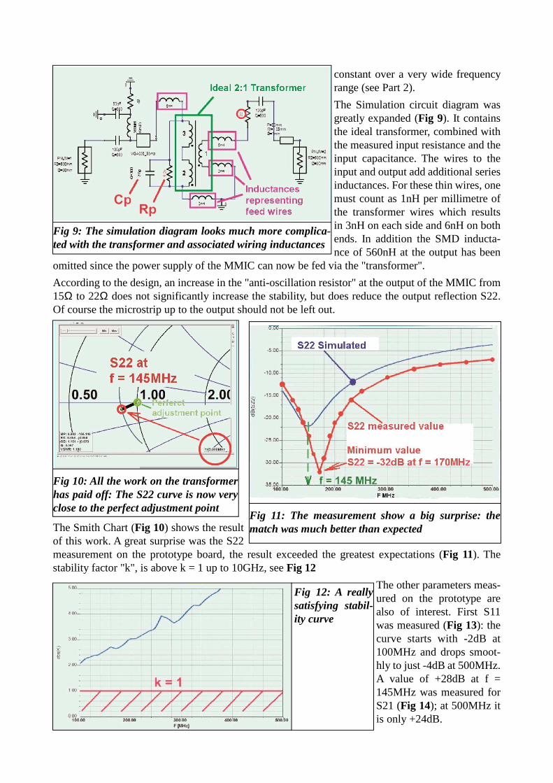
the stability. An attempt was made toset the minimum noise figure at145MHz and to optimise noise figureNF. It has sufficient stability to10GHz resulting from in a small addit-ional 15Ω resistor in the output circuit(but close to the output pin of theMMICs). The grounding coplanarwaveguide with a conductor width of0.59mm, a gap of 1mm on each sideand a length of 32.5mm was not miss-ing in the simulation.
The resulting noise characteristics (seeFig 4) are of course a dream! Howe-
ver, one had to check on a prototype whether this is true - after all, no noise parameters are containedin the S parameter file for this frequency range. In these circumstances the simulation program
Fig 2: The 1 to 1.7GHz amplifier in its aluminium housing
Fig 3: These marked changes make it a 2m LNA
Fig 5: This does not affect stability problems upto 10GHz
Fig 4: This simulated noise figure can not bebelieved (see text)
proceeds by simply applying a lineardecrease of the noise with decreasingfrequency!
Also the required stability (k greaterthan 1 up to 10GHz) is not an issuewith the 15Ω resistor in the outputcircuit - as can be seen in Fig 5.
The simulated S-parameters for thisfrequency range are also of no conc-ern (Fig 6).
1.2. Improving the Output Reflection S22
You cannot change anything at the input of an amplifier after a successful noise adjustment, but theoutput can be optimised without disturbing the noise characteristics. To do this, simulate the circuitwithout the 50Ω line at the output in order to directly determine the parameters of the MMIC outputpin 7. If we now represent S22 in the Smith chart (Fig 7), we see:
At f = 145MHz, S22 results in an output impedance which can be represented by a circuit with R =
180Ω in series with C = 1.87 pF. If a transformer with the voltage ratio ü = 2: 1 is inserted there theimpedance components change by a factor of 22 = 4. The real part of S22 is reduced to 180Ω / ü2 =45Ω and the capacity naturally increases to C = (1.87pF) x 4 = 7.5pF.
This can be compensated by an additional inductance. The result is a substantially smaller reflectionS22. The development of the appropriate transformer is the subject of Part 2.
The output impedance of the first prototype was measured with a BOONTON RX meter in the rangefrom 80MHz to 160MHz. This gave a constant input capacitance of 2.6 pf. In the range of 140 to160MHz the loss resistance of the ferrite material is a parallel resistance between 5 and 5.5kΩ (Fig8).
This measured input impedance (2.6 pF in parallel with approximately 5.2kΩ) can now be combinedwith an ideal 2: 1 voltage transformer and used in the simulation since the transmission ratio remains
Fig 6: These are the S parameters up to 1GHz that are ofinterested for operation in the 2m band
Fig 8: Finally the measurements of the transfo-rmer input capacitance and resistance
Fig 7: The Smith Chart must be expanded to seeand use the S22 details
constant over a very wide frequencyrange (see Part 2).
The Simulation circuit diagram wasgreatly expanded (Fig 9). It containsthe ideal transformer, combined withthe measured input resistance and theinput capacitance. The wires to theinput and output add additional seriesinductances. For these thin wires, onemust count as 1nH per millimetre ofthe transformer wires which resultsin 3nH on each side and 6nH on bothends. In addition the SMD inducta-nce of 560nH at the output has been
omitted since the power supply of the MMIC can now be fed via the "transformer".
According to the design, an increase in the "anti-oscillation resistor" at the output of the MMIC from15Ω to 22Ω does not significantly increase the stability, but does reduce the output reflection S22.Of course the microstrip up to the output should not be left out.
The Smith Chart (Fig 10) shows the resultof this work. A great surprise was the S22measurement on the prototype board, the result exceeded the greatest expectations (Fig 11). Thestability factor "k", is above k = 1 up to 10GHz, see Fig 12
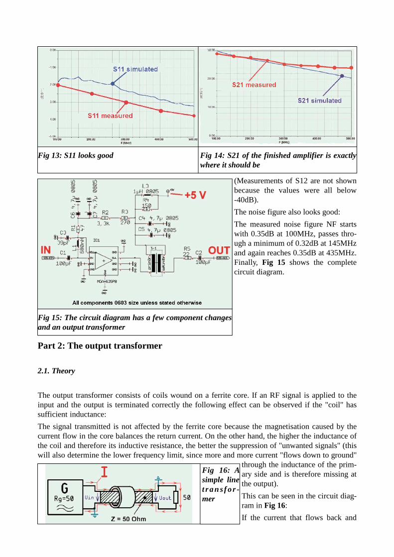
The other parameters meas-ured on the prototype arealso of interest. First S11was measured (Fig 13): thecurve starts with -2dB at100MHz and drops smoot-hly to just -4dB at 500MHz.A value of +28dB at f =145MHz was measured forS21 (Fig 14); at 500MHz itis only +24dB.
Fig 9: The simulation diagram looks much more complica-ted with the transformer and associated wiring inductances
Fig 10: All the work on the transformerhas paid off: The S22 curve is now veryclose to the perfect adjustment point
Fig 11: The measurement show a big surprise: thematch was much better than expected
Fig 12: A reallysatisfying stabil-ity curve
(Measurements of S12 are not shownbecause the values were all below-40dB).
The noise figure also looks good:
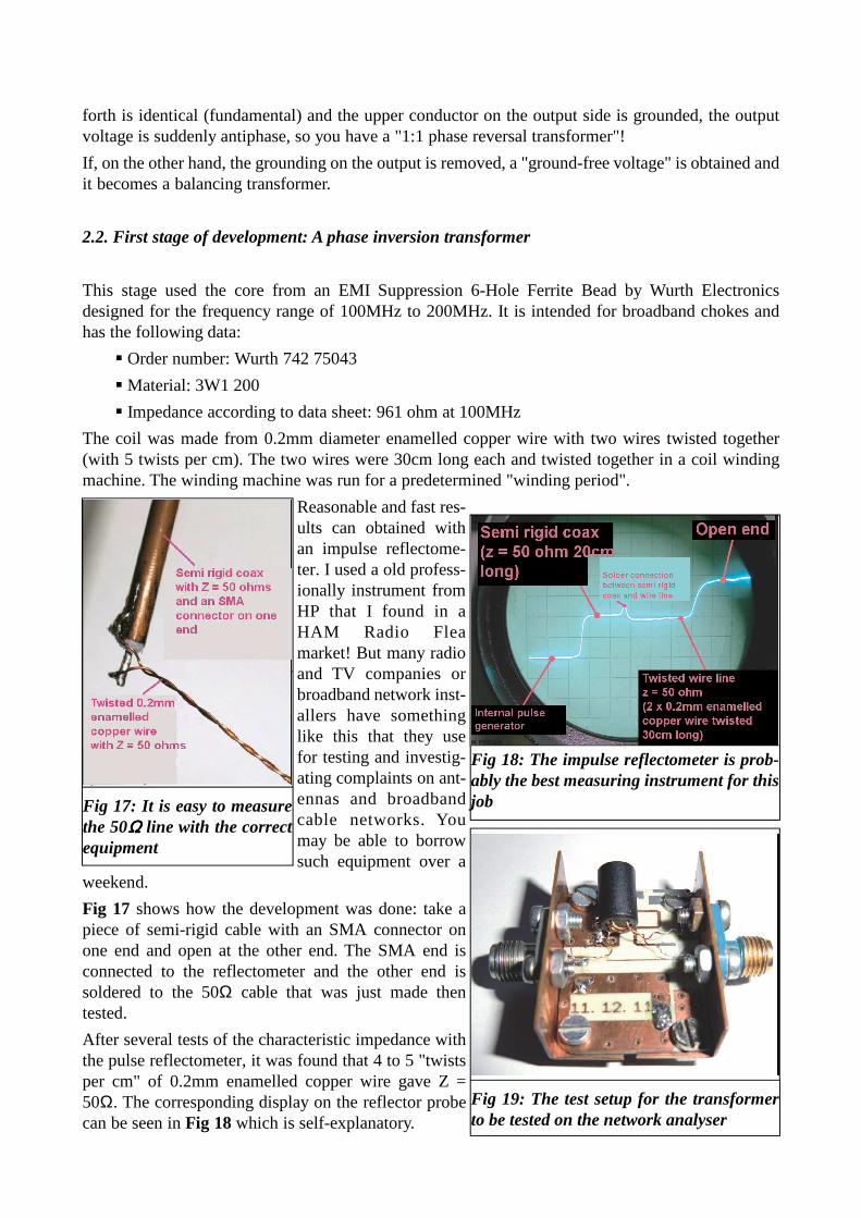
The measured noise figure NF startswith 0.35dB at 100MHz, passes thro-ugh a minimum of 0.32dB at 145MHzand again reaches 0.35dB at 435MHz.Finally, Fig 15 shows the completecircuit diagram.
Part 2: The output transformer
2.1. Theory
The output transformer consists of coils wound on a ferrite core. If an RF signal is applied to theinput and the output is terminated correctly the following effect can be observed if the "coil" hassufficient inductance:
The signal transmitted is not affected by the ferrite core because the magnetisation caused by thecurrent flow in the core balances the return current. On the other hand, the higher the inductance ofthe coil and therefore its inductive resistance, the better the suppression of "unwanted signals" (thiswill also determine the lower frequency limit, since more and more current "flows down to ground"
through the inductance of the prim-ary side and is therefore missing atthe output).
This can be seen in the circuit diag-ram in Fig 16:
If the current that flows back and
Fig 14: S21 of the finished amplifier is exactlywhere it should be
Fig 13: S11 looks good
Fig 15: The circuit diagram has a few component changesand an output transformer
Fig 16: Asimple linet r a n s f or -mer
forth is identical (fundamental) and the upper conductor on the output side is grounded, the outputvoltage is suddenly antiphase, so you have a "1:1 phase reversal transformer"!
If, on the other hand, the grounding on the output is removed, a "ground-free voltage" is obtained andit becomes a balancing transformer.
2.2. First stage of development: A phase inversion transformer
This stage used the core from an EMI Suppression 6-Hole Ferrite Bead by Wurth Electronicsdesigned for the frequency range of 100MHz to 200MHz. It is intended for broadband chokes andhas the following data:
Order number: Wurth 742 75043
Material: 3W1 200
Impedance according to data sheet: 961 ohm at 100MHz
The coil was made from 0.2mm diameter enamelled copper wire with two wires twisted together(with 5 twists per cm). The two wires were 30cm long each and twisted together in a coil windingmachine. The winding machine was run for a predetermined "winding period".
Reasonable and fast res-ults can obtained withan impulse reflectome-ter. I used a old profess-ionally instrument fromHP that I found in aHAM Radio Fleamarket! But many radioand TV companies orbroadband network inst-allers have somethinglike this that they usefor testing and investig-ating complaints on ant-ennas and broadbandcable networks. Youmay be able to borrowsuch equipment over a
weekend.
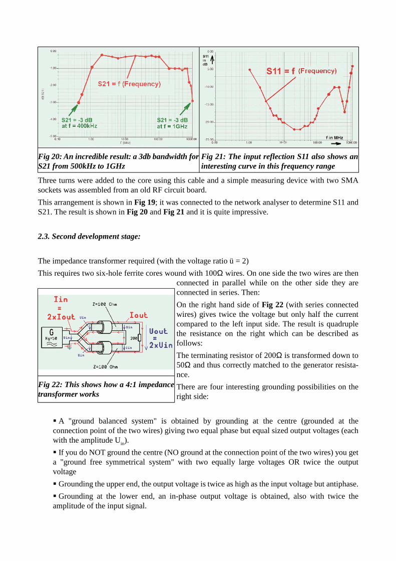
Fig 17 shows how the development was done: take apiece of semi-rigid cable with an SMA connector onone end and open at the other end. The SMA end isconnected to the reflectometer and the other end issoldered to the 50Ω cable that was just made thentested.
After several tests of the characteristic impedance withthe pulse reflectometer, it was found that 4 to 5 "twistsper cm" of 0.2mm enamelled copper wire gave Z =50Ω. The corresponding display on the reflector probecan be seen in Fig 18 which is self-explanatory.
Fig 17: It is easy to measurethe 50ΩΩΩΩ line with the correctequipment
Fig 19: The test setup for the transformerto be tested on the network analyser
Fig 18: The impulse reflectometer is prob-ably the best measuring instrument for thisjob
Three turns were added to the core using this cable and a simple measuring device with two SMAsockets was assembled from an old RF circuit board.
This arrangement is shown in Fig 19; it was connected to the network analyser to determine S11 andS21. The result is shown in Fig 20 and Fig 21 and it is quite impressive.
2.3. Second development stage:
The impedance transformer required (with the voltage ratio ü = 2)
This requires two six-hole ferrite cores wound with 100Ω wires. On one side the two wires are thenconnected in parallel while on the other side they areconnected in series. Then:
On the right hand side of Fig 22 (with series connectedwires) gives twice the voltage but only half the currentcompared to the left input side. The result is quadruplethe resistance on the right which can be described asfollows:
The terminating resistor of 200Ω is transformed down to50Ω and thus correctly matched to the generator resista-nce.
There are four interesting grounding possibilities on theright side:
A "ground balanced system" is obtained by grounding at the centre (grounded at theconnection point of the two wires) giving two equal phase but equal sized output voltages (eachwith the amplitude Uin).
If you do NOT ground the centre (NO ground at the connection point of the two wires) you geta "ground free symmetrical system" with two equally large voltages OR twice the outputvoltage
Grounding the upper end, the output voltage is twice as high as the input voltage but antiphase.
Grounding at the lower end, an in-phase output voltage is obtained, also with twice theamplitude of the input signal.
Fig 21: The input reflection S11 also shows aninteresting curve in this frequency range
Fig 20: An incredible result: a 3db bandwidth forS21 from 500kHz to 1GHz
Fig 22: This shows how a 4:1 impedancetransformer works
The biggest problem with this transformer is theavailability of a high quality 100Ω line. There isnothing on The Internet because wires with highquality Teflon insulation are required. So thereseemed no way forward and that was a big problem.In order to obtain the characteristic resistance, a thic-ker wire insulation is required to increase the distancebetween the two twisted wires, thus spoiling the cap-acitance. The result of many experiments was to use“10 x 0.05” litz wire which gave the desired value ofZ = 100Ω with only 4 twist per centimetre. The finalstate of the development is shown in Fig 23. Thecharacteristics of this 100Ω line are shown on thereflectometer.
Two transformers were fabricated and assembled asfollows:
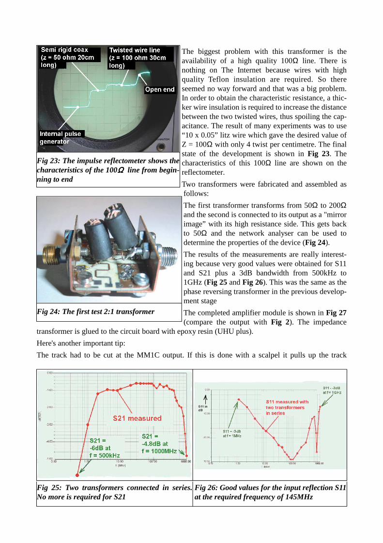
The first transformer transforms from 50Ω to 200Ωand the second is connected to its output as a "mirrorimage” with its high resistance side. This gets backto 50Ω and the network analyser can be used todetermine the properties of the device (Fig 24).
The results of the measurements are really interest-ing because very good values were obtained for S11and S21 plus a 3dB bandwidth from 500kHz to1GHz (Fig 25 and Fig 26). This was the same as thephase reversing transformer in the previous develop-ment stage
The completed amplifier module is shown in Fig 27(compare the output with Fig 2). The impedance
transformer is glued to the circuit board with epoxy resin (UHU plus).
Here's another important tip:
The track had to be cut at the MM1C output. If this is done with a scalpel it pulls up the track
Fig 23: The impulse reflectometer shows thecharacteristics of the 100ΩΩΩΩ line from begin-ning to end
Fig 24: The first test 2:1 transformer
Fig 26: Good values for the input reflection S11at the required frequency of 145MHz
Fig 25: Two transformers connected in series.No more is required for S21

(because the copper layer is not very firmly adhered to the R04350 material). This can only be donewith a thin diamond cutting disc in the famous small handheld drill called "DremeI”
The same applies to drilling holes: This should be done ONLY with carbide drills and ONLY withthe highest speed with the PCB on a hard wood surface. Care should be taken to prevent the drillhitting and damaging the PCB when drilling the large holes for the fastening screws.
The layout of the finished board is shown in Fig 28. It is 30 mm x 50 mm and specially prepared forthe new module. A board for the 1 GHz amplifier was modified at the marked point by cutting theoutput track.
Finally finished - this part was so interesting but tiring.
Part 3: What other people say
In addition to acknowledging words, the question often arose:
What does the amplifier support at the input? How is it protected against over voltage or staticelectricity when connected to an antenna?
These are justifiable concerns and therefore it was necessary to think about this in order to prevent athreat.
3.1. Considerations for the permissible input level
If you take a look at a modern DVT stick (as used for an SDR) you will find a small three leg SMDdevice in an S0T23 package that contains two back-to-back diodes. When Schottky diodes are usedthe peak value of the input signal is approximately 0.4V. The recovery times for such modern diodes(usually below 100 picoseconds) works well into the GHz range and the small self-capacitance ofeach diode (usually approximately 0.5pF) keeps the deterioration of the input reflection withintolerable limits.
The MGA635-P8 has been designed for the "OlP3" (third order output intercept point) as well as the"O1dB" (output 1dB compression point) from 1.9GHz to 3.5GHz
To get to the values for 145MHz consider the following:
At 1.96Hz the O1dB value is about +19.5dBm then for the circuit with an amplification ofapproximately +19 to 19.5dB (according to the data sheet and my own simulations) this means aninput level of approximately zero dBm.
Fig 28: The PCB must be modified by hand asshown for the 145MHz amplifier
Fig 27: The completed 2m amplifier
Since the O1dB value changes very little above that frequency (that indicates the start of overloadingthe final stages) it should also be of the same order of magnitude at 145MHz or only just under it.However, the gain there has risen to +29dB and so the 1dB compression occurs with a 10dB lowerinput level (-10dBm).
It is assumed that the protection diodes do not cause any distortion to the input at this frequency. Thelevel of -10dBm corresponds to a voltage of 70.8mV or a peak value of almost exactly 100mV. ASPICE simulation was used to determine:
If the Schottky diodes will cause any problems
If the higher level and the resulting limiting effect cause additional harmonics in the spectrum.
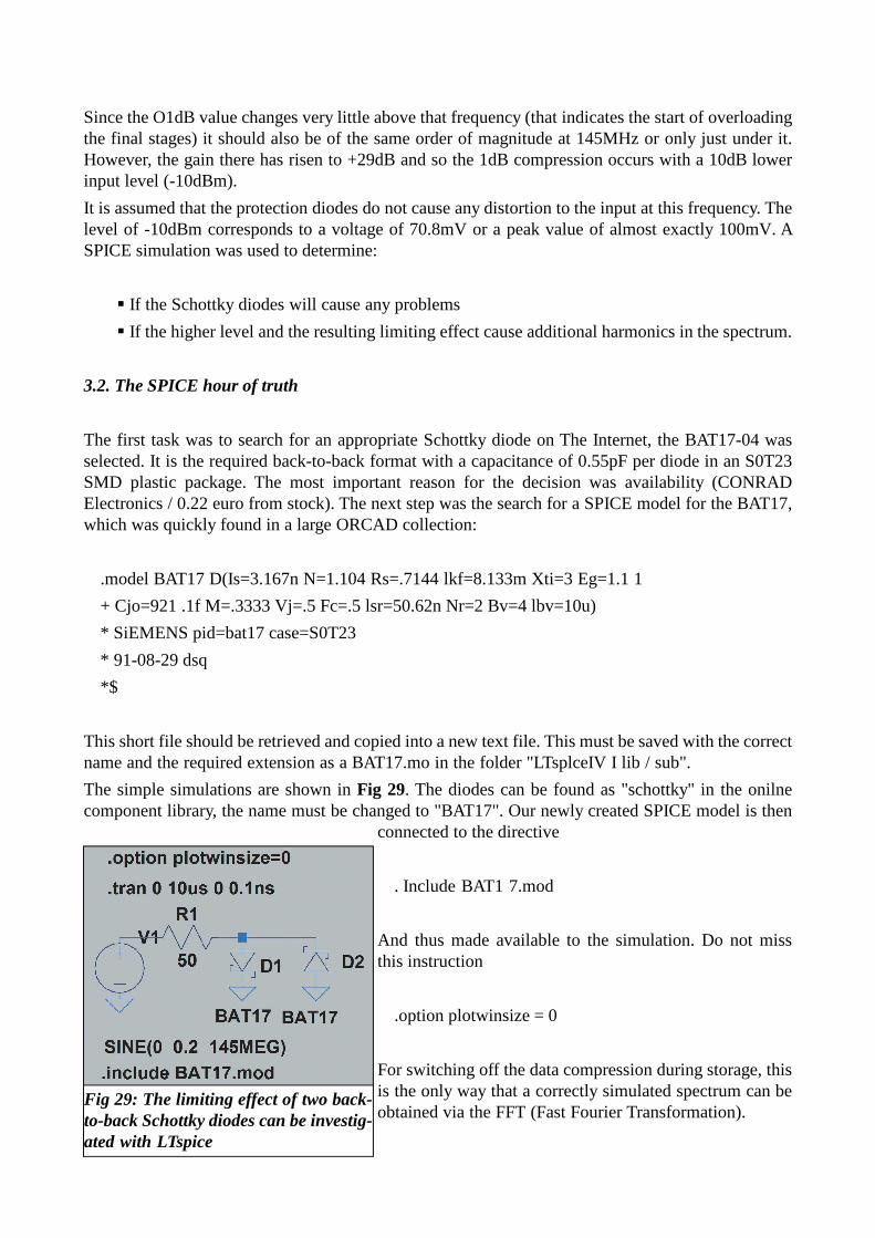
3.2. The SPICE hour of truth
The first task was to search for an appropriate Schottky diode on The Internet, the BAT17-04 wasselected. It is the required back-to-back format with a capacitance of 0.55pF per diode in an S0T23SMD plastic package. The most important reason for the decision was availability (CONRADElectronics / 0.22 euro from stock). The next step was the search for a SPICE model for the BAT17,which was quickly found in a large ORCAD collection:
.model BAT17 D(Is=3.167n N=1.104 Rs=.7144 lkf=8.133m Xti=3 Eg=1.1 1
+ Cjo=921 .1f M=.3333 Vj=.5 Fc=.5 lsr=50.62n Nr=2 Bv=4 lbv=10u)
* SiEMENS pid=bat17 case=S0T23
* 91-08-29 dsq
*$
This short file should be retrieved and copied into a new text file. This must be saved with the correctname and the required extension as a BAT17.mo in the folder "LTsplceIV I lib / sub".
The simple simulations are shown in Fig 29. The diodes can be found as "schottky" in the onilnecomponent library, the name must be changed to "BAT17". Our newly created SPICE model is then
connected to the directive
. Include BAT1 7.mod
And thus made available to the simulation. Do not missthis instruction
.option plotwinsize = 0
For switching off the data compression during storage, thisis the only way that a correctly simulated spectrum can beobtained via the FFT (Fast Fourier Transformation).
Fig 29: The limiting effect of two back-to-back Schottky diodes can be investig-ated with LTspice
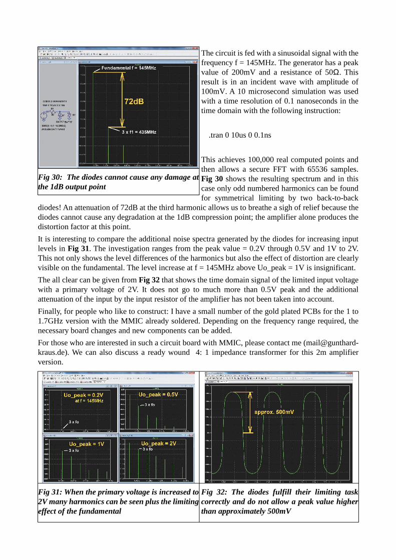
The circuit is fed with a sinusoidal signal with thefrequency f = 145MHz. The generator has a peakvalue of 200mV and a resistance of 50Ω. Thisresult is in an incident wave with amplitude of100mV. A 10 microsecond simulation was usedwith a time resolution of 0.1 nanoseconds in thetime domain with the following instruction:
.tran 0 10us 0 0.1ns
This achieves 100,000 real computed points andthen allows a secure FFT with 65536 samples.Fig 30 shows the resulting spectrum and in thiscase only odd numbered harmonics can be foundfor symmetrical limiting by two back-to-back
diodes! An attenuation of 72dB at the third harmonic allows us to breathe a sigh of relief because thediodes cannot cause any degradation at the 1dB compression point; the amplifier alone produces thedistortion factor at this point.
It is interesting to compare the additional noise spectra generated by the diodes for increasing inputlevels in Fig 31. The investigation ranges from the peak value = 0.2V through 0.5V and 1V to 2V.This not only shows the level differences of the harmonics but also the effect of distortion are clearlyvisible on the fundamental. The level increase at f = 145MHz above Uo_peak = 1V is insignificant.
The all clear can be given from Fig 32 that shows the time domain signal of the limited input voltagewith a primary voltage of 2V. It does not go to much more than 0.5V peak and the additionalattenuation of the input by the input resistor of the amplifier has not been taken into account.
Finally, for people who like to construct: I have a small number of the gold plated PCBs for the 1 to1.7GHz version with the MMIC already soldered. Depending on the frequency range required, thenecessary board changes and new components can be added.
For those who are interested in such a circuit board with MMIC, please contact me ([email protected]). We can also discuss a ready wound 4: 1 impedance transformer for this 2m amplifierversion.
Fig 30: The diodes cannot cause any damage atthe 1dB output point
Fig 32: The diodes fulfill their limiting taskcorrectly and do not allow a peak value higherthan approximately 500mV
Fig 31: When the primary voltage is increased to2V many harmonics can be seen plus the limitingeffect of the fundamental

Literature:
[1] Development of a preamplifier from 1 to 1.7GHz with a noise figure of 0.4 dB, Gunthard Kraus,DG8GB. VHF Communications Magazine, 2/2013 pages 90 - 101
[2] A low noise preamplifier for the 70cm band with a gain of 25dB and a noise figure ofapproximately 0.4dB, Gunthard Kraus, DG8GB, VHF Communications Magazine, 4/2013 pages201 - 213
[3] Student version of the well-known Microwave CAD software ANSOFT Designer. ANSOFT isofficially no longer available but the company has allowed the program to be downloaded from theauthor's homepage (www.gunthard-kraus.de) (Attention: more than 110 megabytes)