a high-efficiency, auto mode-hop, variable-voltage, ripple ... · variable-voltage, ripple control...
TRANSCRIPT

1
A High-Efficiency, Auto Mode-Hop, Variable-Voltage, Ripple Control Buck Converter
Ehsan Rokhsat-Yazdi*, Ali Afzali-Kusha†, and Massoud Pedram** †*Nanoelectronics Center of Excellence, School of Electrical and Computer Engineering, University of
Tehran, Tehran, Iran **Department of Electrical Engineering, University of Southern California, Los Angeles, CA, U.S.A.
Abstract
In this paper, a simple yet efficient auto mode-hop ripple control structure for buck converters with light load operation
enhancement is proposed. The converter, which operates under a wide range of input and output voltages, makes use of a state-dependent hysteretic comparator. Depending on the output current, the converter automatically changes the operating mode. This improves efficiency and reduces the output voltage ripple for a wide range of output currents for given input and output voltages. The sensitivity of the output voltage to the circuit elements is less than 14%, which is seven times lower than that for conventional converters. To assess the efficiency of the proposed converter, it is designed and implemented with commercially available components. The converter provides an output voltage in the range of 0.9V to 31V for load currents of up to 3A when the input voltage is in the range of 5V to 32V. Analytical design expressions which model the operation of the converter are also presented. This circuit can be implemented easily in a single chip with an external inductor and capacitor for both fixed and variable output voltage applications. Key words: Auto Mode-Hop, Buck Converter, High-Efficiency, Ripple Control, Variable-Voltage
I. INTRODUCTION
DC voltage converters that operate with a wide range of
input and output voltages have many applications. These voltage converters can be used in regulators and variable power supplies to reduce power dissipation, for example, on the printed circuit boards of computers. They can also be employed in low-power systems that employ the DVFS (dynamic voltage and frequency scaling) technique whereby, depending on the workload of the system, the supply voltage (and correspondingly, the clock frequency) of the system are changed to match the workload characteristics [1]. On the other hand, systems that use batteries or have limited energy sources (e.g., solar cell powered systems) require voltage converters with high efficiency and high quality at a low cost [2].
Buck converters, as one of the most widely used converters, have been investigated with different structures and control methods (see, e.g., [3]-[16]). In these converters, voltage
conversion is based on applying a voltage pulse (with a specific duty cycle and frequency) to a low pass filter. The DC value of the applied signal, which is dependent on the duty cycle, will pass through the filter, creating the output voltage. To achieve the desired output voltage value and quality, a control unit is used. Many different controllers have been suggested for these circuits (see, e.g., [3]-[9]). The control circuit can be designed using analog or digital approaches although the latter is typically more involved [10]-[12]. Among the different parameters of buck converters, power loss and efficiency have received a great deal of attention (see, e.g., [13],[17]).
Fig. 1. The circuit diagram of buck converter [5]. The circuit diagram of a buck converter is shown in Fig. 1,
where a switch is used for generating the pulses [5]. In this
Manuscript received August 1, 2009; revised Jan. 21, 2010 †Corresponding Author: [email protected] Tel: +98-21-8208-4920, Fax: +98-21-8877-8690, Univ. of Tehran
*School of Electrical and Computer Eng., University of Tehran, Iran

2 Journal of Power Electronics, Vol. 10, No. 2, March 2010 circuit, the output low pass filter consists of an L and a C while RL is the equal series resistance of the inductor (L) and RC is the equivalent series resistance of the capacitor (C). The switch is turned on and off by a driver which is controlled by a control unit. The frequency of the voltage pulses generated by this switch is called the switching frequency. By increasing the switching frequency, a smaller inductor and a simpler output filter may be used [14]. However, increasing the switching frequency causes the loss in the switch driver to become more than that of the main switch. The former loss may be reduced by resonant gate driver techniques [15]-[16].
In [2], the efficiency characteristic of a dc-dc buck converter as a function of the load current is divided into three regions. Here, we briefly present a discussion of [2] regarding this characteristic. The three regions of a typical efficiency curve for a dc–dc converter are shown in Fig. 2. In region I (high loads) the losses are mainly due to the conduction losses which depend on the load current. In region II (light loads), the major power losses are from the V–I overlap and conduction losses induced by the current ripple. The V–I overlap switching losses are proportional to the load current, input voltage, and switching frequency. One of the approaches for eliminating this loss mechanism is soft switching where the power transistor is switched when either its voltage (zero-voltage switching (ZVS)) or its current is zero (zero-current switching (ZCS)) [18]-[20]. Other methods include quasi-square-wave (QSW) [20], zero-current transition (ZCT) [2], and zero-voltage transition (ZVT) [21]. While the conduction losses caused by the current ripple normally remain constant, the overlap losses decrease with a reduction in load current. Therefore, at lower load currents, the conduction losses become dominant. In this region, a combination of soft switching, which eliminates the overlap losses, and adaptive current ripple control, which eliminates current ripple conduction losses, is the best existing power-saving technique [2]. In region III (very light loads), the gate-drive losses which originate from charging and discharging the gate capacitances of the power transistors become dominant. To minimize the total losses in this region, one should decrease the switching frequency. To achieve high efficiency in this region, the use of a sleep mode has been patented [22] and is purportedly in use. To improve the efficiency of the converter in all regions of operation, a load-dependent mode-hopping strategy [23], is proposed in [2]. It makes use of the tradeoffs between conduction and switching losses to maintain a high efficiency over a wide load–current range. This technique is briefly explained here. The current waveforms (ripples) of the inductor in the three operational modes are shown in Fig. 3. In region I (high loads), the majority of the total power losses are
Fig. 2. Efficiency versus load current for dc–dc converters [2]. In
each region, the mechanism dominating the loss is given. determined by the load current itself. The control strategy used for this region is the conventional synchronous continuous-conduction mode (CCM) with constant current ripple and hard switching (Fig. 3(a).) In region II (light loads), the converter hops from CCM to synchronous discontinuous-conduction mode (DCM). This is achieved by increasing the current ripple until enough reverse inductor current is available to achieve QSW ZVS. The higher current ripple gives rise to increased conduction losses which are balanced by the reduced V–I overlap losses. As a result, the efficiency is not degraded. In addition, instead of keeping the current ripple constant, it is reduced as the load current decreases (Fig. 3(b)). This helps to adaptively reduce the conduction losses, considerably improving the light-load efficiency. In region III (very light loads), the frequency increases to the point where the gate-driver losses start to deteriorate the efficiency. Therefore, the frequency is lowered at very light loads, reverting back to hard switching of the asynchronous DCM. Note that in this regime, the V–I overlap losses are negligible. Additionally, in this region, constant peak current control [24] is used. As a result, the frequency decreases proportionally with the load current (Fig. 3(c)). This way, the efficiency is kept approximately constant. In [2] the mode-hopping operation is performed manually. However, in this paper, we propose a structure for an automatic mode change ripple control buck converter with a simple structure. This converter has high efficiency with large variations in the load current and in the input and output voltage. We use a simple ripple control structure with a state-dependent hysteretic comparator. The comparator minimizes sensitivity to the operating conditions and elements values.
The remainder of this paper is organized as follows. In Section II, we outline the main structure of the proposed converter while the system operation of the circuit and its operating modes are explained in Section III. We present some analytical expressions for the converters in Section IV and

A High-Efficiency, Auto Mode-Hop, Variable-Voltage, Ripple … 3
discuss the results in Section V. Finally, the summary and conclusion are given in Section VI.
Fig. 3. Current waveforms (ripples) of the filter inductor in three
operation modes. (a) Mode 1 (CCM with constant current ripple). (b) Mode 2 (synchronous DCM with adaptive current ripple). (c) Mode 3 (asynchronous DCM with constant peak current) [2].
II. PROPOSED RIPPLE-CONTROL BUCK CONVERTER
A block diagram of the proposed buck converter system
whose control mechanism is based on the ripple control of the output voltage is shown in Fig. 4. It utilizes a ripple control structure where the switching frequency and the operating mode are automatically varied depending on the input and output voltages and the output current under the light load and very light load conditions. The ripple control method is a simple, yet flexible, control structure for this purpose [2], [25]-[27]. Fig. 5 depicts a circuit for the proposed buck converter, which has the common buck structure as the main part. For the power switch in this part, both P- and N-type power MOSFETs may be utilized. To turn on the N-type power MOSFET, a voltage higher than Vin is required to drive the transistor gate, and hence the driving circuit will be more complex than that of a P-type power MOSFET which requires a zero voltage. Thus, we have opted to use a P-type power MOSFET due to its simpler gate driver circuit. Another part of the system is a state-dependent hysteretic voltage comparator, which compares the output voltage and the reference voltage to change the operating mode based on the system state.
Fig. 4. The block diagram of the proposed converter system.
Fig. 5. The circuit diagram for the proposed buck converter.
III. CIRCUIT OPERATION ANALYSIS
To explain the operational principles of the proposed circuit, we consider the two states (ON and OFF) for the power switch (see Fig. 6). In the ON state (the first state), the output voltage is lower than Vref+∆ and the comparator output voltage is near GND, turning on the power switch. In this case, the inductor current which charges the capacitor and supplies the load current rises. In this state, the negative input voltage of the comparator, VX, which is the comparator reference voltage, is obtained by adding the limited and scaled voltage of VA, which is ∆, to the reference voltage (Vref). We use D2 (D3) to limit the voltage across D1 (VA) and use R2 (R3) to scale the

4 Journal of Power Electronics, Vol. 10, No. 2, March 2010 forward bias voltage, γ, of D3 (D2) achieving a fixed positive (negative) change, ∆, around Vref in the OFF (ON) state. Notice that the value of ∆ does not depend on the input voltage or switch on-state resistance.
When the output voltage reaches Vref+∆, the circuit changes its state to the OFF state and the comparator output voltage becomes close to VCC, turning off the power switch. This causes the inductor current to pass through D1 turning it on (the current loop becomes closed). In this state, VA becomes –γ where by limiting and scaling VA, the negative input voltage of the comparator, VX, will change to Vref–∆. Then, until the output voltage is higher than Vref–∆, the circuit will be in the OFF state. When the output voltage reaches Vref–∆, the state of the circuit will change to the ON state. The DC level of the output voltage is equal to Vref while the ac level of the output voltage is a triangular ac voltage with the amplitude of ∆. Having a lower ∆ makes the output voltage ripple lower which enhances the quality of the output voltage. Fig. 7 (8) illustrates the simulation (experimental) results of the voltages and the currents of different nodes in the circuit.
Fig. 6. The operating states of the buck converter circuit: (a) power
switch is ON, (b) power switch is OFF. As stated earlier, in conventional continuous-conduction
mode buck converters, if the load current becomes lower than the critical current, the operating mode will change to the asynchronous DCM. This mode change adversely affects the converter efficiency and output ripple. One of the advantages of the proposed circuit is that when the load current is lower than the critical current, the switching frequency of the circuit will increase. Therefore, the ripple of the inductor current is decreased and the operating mode is changed to the synchronous DCM mode. Under this condition, when the current of the inductor in the OFF state approaches zero (the boundary between the continuous and discontinuous modes), VA rises (this is because the inductor current is zero) changing VX to Vref+Δ. This in turn makes the circuit change
Fig. 7. The voltages and currents of different nodes in the buck converter circuit when the load current is higher than the critical current. Simulation conditions: T = 27ºC, Vin = 32V, Vout = 16V, Iload = 1A, ∆ = 6.2mV, L = 200µH, RL = 0.1Ω, RC = 0.1Ω, C = 220µF.
Fig. 8. The voltages and currents of different nodes in the buck converter circuit when the load current is higher than the critical current. Experimental conditions: T = 27ºC, Vin = 32V, Vout = 16V, Iload = 1A, ∆ = 6.2mV, L = 200µH, RL = 0.1Ω, RC = 0.1Ω, C = 220µF. its state to the ON state ("state toggling"). This automatically raises the switching frequency and changes the behavior to zero voltage switching (ZVS). In zero voltage switching, when the voltage across the switch becomes zero, the switch is turned on decreasing the switching loss. Although zero voltage switching has been used previously to increase efficiency (see, e.g., [18], [19]), the proposed converter changes its operation
A High-Efficiency, Auto Mode-Hop, Variable-Voltage, Ripple … 5
automatically to ZVS only under light load conditions. This increases the conversion efficiency for light loads. Fig. 9 and 10 show the experimental waveforms of the voltages and currents including the case when the load current is lower than the critical current (in this case the critical current is 750mA).
Under the very light load condition, the switch ON time, which depends on the delays of the control system and the switch driver, remains nearly constant. Therefore, the converter will operate in the asynchronous DCM mode with a constant current ripple.
Fig. 9. The voltage and current waveforms for the case when the
load current is lower than the critical current. Simulation conditions: T = 27ºC, Vin = 32V, Vout = 16V, Iload = 0.5A, ∆ = 6.2mV, L = 20μH, RL = 0.1Ω, RC = 0.01Ω, C = 220μF.
Fig. 10. The voltage and current waveforms for the case when the
load current is lower than the critical current. Experimental conditions: T = 27ºC, Vin = 32V, Vout = 16V, Iload = 0.5A, ∆ = 6.2mV, L = 20μH, RL = 0.1Ω, RC = 0.01Ω, C = 220μF.
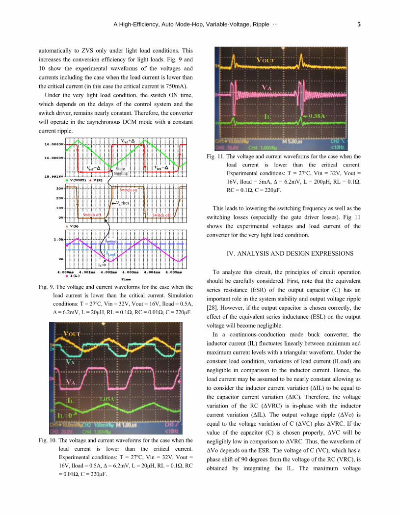
Fig. 11. The voltage and current waveforms for the case when the
load current is lower than the critical current. Experimental conditions: T = 27ºC, Vin = 32V, Vout = 16V, Iload = 5mA, ∆ = 6.2mV, L = 200μH, RL = 0.1Ω, RC = 0.1Ω, C = 220μF.
This leads to lowering the switching frequency as well as the
switching losses (especially the gate driver losses). Fig 11 shows the experimental voltages and load current of the converter for the very light load condition.
IV. ANALYSIS AND DESIGN EXPRESSIONS
To analyze this circuit, the principles of circuit operation
should be carefully considered. First, note that the equivalent series resistance (ESR) of the output capacitor (C) has an important role in the system stability and output voltage ripple [28]. However, if the output capacitor is chosen correctly, the effect of the equivalent series inductance (ESL) on the output voltage will become negligible.
In a continuous-conduction mode buck converter, the inductor current (IL) fluctuates linearly between minimum and maximum current levels with a triangular waveform. Under the constant load condition, variations of load current (ILoad) are negligible in comparison to the inductor current. Hence, the load current may be assumed to be nearly constant allowing us to consider the inductor current variation (ΔIL) to be equal to the capacitor current variation (ΔIC). Therefore, the voltage variation of the RC (ΔVRC) is in-phase with the inductor current variation (ΔIL). The output voltage ripple (ΔVo) is equal to the voltage variation of C (ΔVC) plus ΔVRC. If the value of the capacitor (C) is chosen properly, ΔVC will be negligibly low in comparison to ΔVRC. Thus, the waveform of ΔVo depends on the ESR. The voltage of C (VC), which has a phase shift of 90 degrees from the voltage of the RC (VRC), is obtained by integrating the IL. The maximum voltage

6 Journal of Power Electronics, Vol. 10, No. 2, March 2010 variations of the C and RC are obtained from, respectively:
CFI
dtIC
V C
TCC ××
==Δ ∫ 41 max,
2/max, (1)
CCR RIV ×=Δ max,max, (2)
where F (1/T) is the switching frequency of the converter. If ΔVC is much larger than ΔVRC (because of a small C), when the output voltage reaches Vref+Δ, the switch will turn off and iL will decrease but Vo will keep increasing due to the 90 degrees phase shift between the voltage and the current of the self. This gives rise to a large increase in the output voltage ripple.
In all buck converters, the value of the output capacitor plays an important role in decreasing the output ripple. Choosing a larger capacitance causes a lower voltage variation on the C. Besides, a large output capacitor has a lower ESR, thereby reducing the output ripple due to this resistor. A proper value of the C (for a low ΔVC) may be selected by having the cut-off frequency of the low-pass filter (consisting of the RC and C) to be 10 times larger than the circuit switching frequency, i.e.:
CRFC
×≥
59.1 (3)
If this condition is satisfied, ΔVo will be proportional to ΔVRC which is verified by our simulation results for the circuit. Fig. 12 and Fig. 13 report the effects of the C on the switching frequency and ΔVo (ripple). The results show that if we select a value of C that is more than 68µF (see Eq. (3)), ΔVo will be minimized while the switching frequency will be approximately independent of the C variations.
120
140
160
180
200
220
240
260
280
300
1 10 100 1000
OUTPUT CAPACITANCE (uF)
SWIC
HIN
G F
REQ
UEN
CY
(KH
z)
68
Fig. 12. The effect of the output capacitance on the switching
frequency. Simulation conditions: T = 27ºC, Vin = 32V, Vout = 16V, Iload = 1A, ∆ = 5mV, L = 200μH, RL = 0.1Ω, RC = 0.1Ω.
10
100
1000
1 10 100 1000
OUTPUT CAPACITANCE (uF)
OU
TPU
T V
OLT
AG
E R
IPPL
E (m
V)
68
Fig. 13. The effect of the output capacitor size on the output
voltage ripple. Simulation conditions: T = 27ºC, Vin = 32V, Vout = 16V, Iload = 1A, ∆ = 5mV, L = 200μH, RL = 0.1Ω, RC = 0.1Ω.
Based on the above discussion, we have drawn the output
voltage waveform with a triangular ripple characteristic as depicted in Fig. 14. The figure also identifies two other important delay parameters. The delays, denoted as tD1 and tD2, are those associated with the control circuit, the MOSFET driver, and the MOSFET switch. The delays which affect the output voltage ripple and the switching frequency, have a profound (negligible) effect at higher (lower) switching frequencies. As shown in Fig. 14, except for the durations of tD1 and tD2, the control mechanisms keep the output voltage between Vref+Δ and Vref–Δ. During tD1 (tD2), the output voltage changes between Vref+Δ and VH (Vref–Δ and VL), thereby increasing the output ripple. These durations may be approximated by:
tD1 = tDS(OFF) + tCR + tDR (4) tD2 = tDS(ON) + tCF + tDF (5)
where tDS(OFF) is the MOSFET turn off delay, tDS(ON) is the MOSFET turn on delay, tCR is the comparator output rise time, tCF is the comparator output fall time, tDR is the MOSFET driver rise time, and tDF is the MOSFET driver fall time. These parameters can be determined from the component characteristic data (such as the manufacturer’s datasheets) which can subsequently be used in Eq. (4) and Eq. (5) to determine tD1 and tD2. The durations of tD1 and tD2 may also be determined more accurately from simulations. For the components used in our design, the calculated tD1 (tD2) is 186ns (95ns) which is 5% (9%) less than the results obtained from the simulation. If the calculated values of tD1 and tD2 have an error of less than 10%, the output ripple and frequency calculation errors should be less than 1% (see Eq. (10) and Eq. (16)).

A High-Efficiency, Auto Mode-Hop, Variable-Voltage, Ripple … 7
Fig. 14. The output voltage waveform.
To calculate VL and VH, two assumptions are made. First,
since the durations are short, we can safely assume that the input and output voltages are constants. Second, since the load current variation is small, we assume that the voltage variation of RL in comparison to the inductor voltage variation is small. Therefore, the inductor current will change linearly as:
LVtI L
L×Δ
=Δ (6)
where VL denotes the inductor voltage, L is the inductance, and Δt denotes the ON or OFF time duration. As shown before, the output voltage ripples are equal to the voltage variation of the RC which is in turn proportional to the inductor current. More precisely: ΔVout = ΔIL × RC
(7) Therefore:
( )C
LLDoutDrefL R
LRIVVtVV ×⎥⎦
⎤⎢⎣
⎡ ×++×−Δ−= 12
(8) and:
( )C
LLDSoutinDrefH R
LRIVVVtVV ×⎥⎦
⎤⎢⎣⎡ ×−−−×
+Δ+= 1
where VD1 is the D1 forward bias voltage, VDS denotes the drain to source voltage of the switch when it is on, and IL is the average current of the inductor that is equal to the load current. After calculating VH and VL, the ripple (Vripple), the DC voltage (VDC), and the error of the output (Verror) can also be calculated using:
Vripple=VH – VL (10)
2LH
DCVV
V+
= (11)
Verror=Vref – VDC (12)
The output voltage ripple as a function of the output voltage has been depicted in Fig. 15. As can be seen from the results, the ripple voltage is small and it has a low sensitivity to the output and input voltage variations. The simulation results for the error in the output voltage compared to Vref as a function of the load current is shown in Fig. 16 where the output voltage is the running parameter. As can be seen, the load regulation is better than 0.02%. The error of the output voltage, which is positive for low output voltages and negative for high output voltages, is very low.
To obtain the duty cycle and the switching frequency, we should first obtain expressions for toff and ton. By combining Eq. (6) and Eq. (7), we can write:
10
11
12
13
14
15
16
17
0 5 10 15 20 25 30OUTPUT VOLTAGE (V)
OU
TPU
T V
OLT
AG
E R
IPPL
E (m
V)
Calculated, Vin=32VCalculated, Vin=17VSimulated, Vin=32VSimulated, Vin=17V
Fig. 15. The output voltage ripple as a function of the output voltage. Simulation conditions: T = 27ºC, Iload = 1A, ∆ = 5mV, L = 200μH, RL = 0.1Ω, RC = 0.1Ω, C = 220μF.
-1.5
-1
-0.5
0
0.5
1
1.5
2
2.5
100 500 900 1300 1700 2100 2500 2900 3300
OUTPUT CURRENT (mA)
OU
TPU
T V
OLT
AG
E ER
RO
R (m
V)
Vout=5V
Vout=16V
Vout=27V
Fig. 16. The output voltage error as a function of the load current. The running parameter is the output voltage. Simulation conditions: T = 27ºC, Vin = 32V, ∆ = 5mV, L = 200μH, RL = 0.1Ω, RC = 0.1Ω, C = 220μF.
VRLV
VLIt
C
outL××Δ
=×Δ
=Δ (13)

8 Journal of Power Electronics, Vol. 10, No. 2, March 2010
and hence:
CLLDout
LHoff RRIVV
LVVt
××++×−
=)(
)( (14)
CLLDSoutin
LHon RRIVVV
LVVt
××−−−×−
=)(
)( (15)
Using the above expressions, we can calculate the switching
frequency and the duty cycle as:
offon ttF
+=
1 (16)
in
out
offon
onVV
ttt
D ≈+
= (17)
Fig. 17 shows the switching frequency versus the output
voltage level for two different input voltages. As shown in this figure, the frequency is reduced automatically when the output to input voltage ratio is nearly zero or one. The decrease in the switching frequency prevents the generation of the narrow width pulses used for controlling the switch. Therefore, the mechanism for changing the duty cycle is performed easily, yielding high efficiencies for wide ranges of input and output voltages.
The variation of the duty cycle as a function of the output voltage is plotted in Fig. 18 which reveals an almost linear relationship between the duty cycle and the Vout/Vin ratio for a wide range of the output voltages (ignoring the voltage drops on the diode, the switch, and RL). This means that the duty cycle will change automatically with the output voltage without a complex control system. In conventional PWM-based buck converters where the switching frequency is constant, the duty cycles when the output voltage is close to 0 or Vin, may cause narrow pulses. The switch and its driver may not respond to these pulses adequately, thereby limiting the output voltage range. In the case of the proposed converter, the decrease in the frequency for the boundary output voltages prevents the formation of narrow pulses.
In buck converters, a reduction of the load current below the critical current Icritical, causes a change in the circuit operating mode from the CCM to asynchronous DCM mode. The critical current may be calculated as follows:
C
LH
C
outLcritical R
VVRV
II×−
=Δ
×=Δ×≡22
121 (18)
25
75
125
175
225
275
0 5 10 15 20 25 30 35 40 45
OUTPUT VOLTAGE (V)
SWIT
CH
ING
FER
QU
ENC
Y (K
Hz)
Calculated, Vin=32VCalculated, Vin=17VSimulated, Vin=32VSimulated, Vin=17V
Fig. 17. The switching frequency as a function of the output
voltage. The input voltage is the running parameter. Simulation conditions: T = 27ºC, Iload = 1A, ∆ = 5mV, L = 200μH, RL = 0.1Ω, RC = 0.1Ω, C = 220μF.
0
0.1
0.2
0.3
0.4
0.5
0.6
0.7
0.8
0.9
1
0 5 10 15 20 25 30 35
OUTPUT VOLTAGE (V)
DU
TY C
YC
LE
Calculated, Vin=32VCalculated, Vin=17VSimulated, Vin=32VSimulated, Vin=17V
Fig. 18. The duty cycle as a function of the output voltage. The
input voltage is the running parameter. Simulation conditions: T = 27ºC, Iload = 1A, ∆ = 5mV, L = 200μH, RL = 0.1Ω, RC = 0.1Ω, C = 220μF.
50
100
150
200
250
300
350
400
450
500
0 200 400 600 800 1000 1200
OUTPUT CURRENT (mA)
SWIT
CH
ING
FR
EQU
ENC
Y (K
Hz)
Icritical
Continuous Mode
Disc
ontin
uous
Mod
e
Calculated
Simulated
Fig. 19. The switching frequency versus the load current around and below the critical current. Calculated results have been obtained from (14)-(16) and (19). Simulation conditions: T = 27ºC, Vin = 32V, Vout = 16V, ∆ = 5mV, L = 20μH, RL = 0.1Ω, RC = 0.01Ω, C = 220μF.

A High-Efficiency, Auto Mode-Hop, Variable-Voltage, Ripple … 9
In the proposed circuit, because of the state-dependent hysteretic comparator, the operating mode changes from CCM to synchronous DCM for light loads. In our converter, when the load current decreases below the critical current level, the switching frequency increases, the inductor peak current decreases and the converter works with the ZVS method automatically. This decreases both the conduction and switches V-I overlap losses).
Fig. 19 illustrates the results of simulations and calculations for the converter with a critical current level of 750mA. As shown in the figure, when the load current decreases, the frequency increases. As will be seen later in this paper, this feature provides us with a reasonably wide range of output voltages for a given input voltage. Notice that when the output current is lower than 200mA (i.e., under the very light load condition), the switching frequency will decrease and the converter will operate in the asynchronous DCM mode to achieve a higher efficiency. The over estimation of the frequency obtained from the calculations is due to ignoring the parasitic capacitance of the node A.
Note that under the condition that the load current is lower than the critical current, VL becomes higher, thus increasing the frequency (see Fig. 9). The output voltage, the ripple, and the switching frequency should be calculated with this new VL (which is valid only for the continuous mode) which is itself calculated as follows:
CoutHCLH
outHL
RIVRIV
VVV
××−=×Δ−=
Δ−=
2max,
max, (19)
V. RESULTS AND DISCUSSION A converter circuit with the parameters given in Table I was
simulated using OrCAD and implemented with the part numbers of the elements given in Table II. All figures presented in this section report the results obtained by these simulations. Fig. 20 compares the efficiencies of the proposed converter and the conventional linear converter from [3] as a function of the load current for Vin = 32V and Vout = 16V. As is apparent from the figure, when compared to a conventional circuit, the efficiency of the proposed circuit is higher under a wide range of load currents, especially for light loads.
To assess the performance of the proposed converter against other converters, we compared the efficiency and the ripple of our converter with those of the recently published converter in
[2], denoted by "Adaptive ripple QSW + Mode-Hop" here. A comparison between the efficiencies of the two converters is reported in Fig. 21. Similar to [2], we classified the operation of the proposed converter into three modes based on the value of the load current. The three modes are very light load (1mA < Iload < 70mA), light to medium load (70mA < Iload < 400mA), and high load (400mA < Iload). The results reveal a higher efficiency for the proposed converter under the light and very light load conditions. In Fig. 22, the output ripples of the two converters are compared. As is evident from the figure, the ripple of the proposed circuit is considerably lower than that of the other circuit. Furthermore, one should note that the converter in [2] uses manual mode-hopping, which in turn complicates the control system and generates low frequency noise. Since the proposed circuit switches between these modes smoothly and automatically, a higher performance is achieved. Under load variation, the manual mode-hopping control mechanism could lead to the generation of noise which may adversely affect the performance of sensitive circuits, for instance, video and audio circuits. In the proposed circuit, the frequency changes automatically and smoothly, preventing any undesired effect on the sensitive circuitry.
The proposed converter has a very fast (lower than 5μs) load transient response time. Fig 23(a)-(f) show the load transient response between the different modes where the maximum output voltage change (overshoot and undershoot) was lower than 100mV (0.06% of the output voltage).
TABLE I
PARAMETERS OF THE PROPOSED CONVERTER Parameter Value
Vin 5-32V Vout 0.9-30V Iout 1mA-3A C 220µF RC 100mΩ L 200µH
RL 100mΩ Δ 5mV
TABLE II
BASIC ELEMENTS OF THE PROPOSED CONVERTER Element Part number
SW IRF9540 Comparator LM319
D1 1N5819 (× 3) D2 – D3 1N4148

10 Journal of Power Electronics, Vol. 10, No. 2, March 2010
50556065707580859095
100
100 500 900 1300 1700 2100 2500 2900 3300
OUTPUT CURRENT (mA)
EFFI
CIE
NC
Y (%
)
Proposed, SimulationConventional, Simulation
Proposed, ExperimentalConventional, Experimental
Fig. 20. The efficiency as a function of the load current.
Simulation and experimental conditions: T = 27ºC, Vin = 32V, Vout = 16V, ∆ = 5mV, L = 200μH, RL = 0.1Ω, RC = 0.1Ω, C = 220μF.
65
70
75
80
85
90
0 100 200 300 400 500 600 700 800 900 1000OUTPUT CURRENT (mA)
EFFI
CYEN
CY (%
)
Proposed circuit, SimulationAdaptiv ripple QSW + Mode Hop, ExperimentalProposed circuit, Experimental
Mode 1Mode 2
Mode 3
Fig. 21. The efficiency comparison of proposed circuit and
adaptive ripple QSW + Mode-Hop [2]. Simulation and experimental conditions: T = 27ºC, Vin = 5V, Vout = 1.8V, RL = 0.02Ω, RC = 0.075Ω, C = 47μF.
0
10
20
30
40
50
60
70
80
90
0 200 400 600 800 1000OUTPUT CURRENT (mA)
OU
TPU
T V
OLT
AG
E RI
PPLE
(mV
)
.
Proposed circuit, Simulation
Adaptiv ripple QSW + Mode Hop, Experimental
Proposed circuit, Experimental
Mode 3
Mode 2Mode 1
Fig. 22. The output voltage ripple comparison of proposed circuit
and adaptive ripple QSW + Mode-Hop[2]. Simulation and experimental conditions: T = 27ºC, Vin = 5V, Vout = 1.8V, RL = 0.02Ω, RC = 0.075Ω, C = 47μF.
In Fig. 24, the dependence of the output voltage ripple on the
RC (ESR) has been plotted. As may be inferred from these results, the sensitivity of the output voltage ripple on the RC variation is less than 12% for the proposed circuit while it is 100% for the conventional design. The experimental output voltage ripple of the proposed converter was less than 35mV compared to 120mV for the conventional design. This has been achieved by lowering the effect of the ESR on the ripple with the following method. The output voltage ripple is proportional to the ESR (RC). In the proposed circuit, this dependence has been minimized by increasing the switching frequency of the circuit when the RC increases. The frequency increase lowers ΔIL. Since the output voltage ripple is obtained by multiplying the RC by ΔIL, the sensitivity of the output voltage ripple on the ESR becomes small.
Fig. 25 illustrates the effect of variations of the inductor value on the output voltage ripple. The proposed circuit has a much lower sensitivity (<14%) to variations in L than conventional methods (100%). Therefore, in the proposed circuit, inductor saturation gives rise to lower undesirable effects on the output voltage. The range of the output voltage for a given input voltage is given in Fig. 26, which reveals a fairly good regulation. The maximum value of the output voltage is limited by the input voltage level, the control system, the voltage drop on the RL, and the switch, SW. The minimum value of the input voltage is mainly limited by the gate threshold voltage of SW.
VI. CONCLUSION
In this paper, we presented an auto mode-hopping ripple
control buck converter, which operates in a wide range of the input and output voltages and a wide range of output current variations with high efficiency. The operations under the light load and very light load conditions were enhanced by using a state-dependent hysteretic comparator, which changed the operating modes automatically to achieve a high efficiency and a low output voltage ripple. The comparator enabled the converter to support a wide range of load currents. Analytical expressions were presented for different parameters of the converter. The circuit was designed and implemented. The results showed the high efficiency of the circuit and its low sensitivity to circuit elements such as the inductor, the equal series resistance (ESR), the output capacitor, and the inductor saturation. The converter efficiency was high (up to 92%) while the output voltage ripple was very small (less than 25mV). The load regulation was about 0.02% which is an indication of the high performance of the proposed converter.

A High-Efficiency, Auto Mode-Hop, Variable-Voltage, Ripple … 11
(a)
(b)
(c)
(d)
(e)
(f)
Fig 23. Load transient responses. (a) High load to light load: Ihigh load = 1A, Ilight load = 50mA, (b) Light load to high load: Ihigh load = 1A, Ilight load = 50mA, (c) High load to very light load: Ihigh load = 1A, Ivery light load = 5mA, (d) Very light load to high load: Ihigh load = 1A, Ivery light load = 5mA, (e) Light load to very light load: Ilight load= 50mA, Ivery light load=5mA, (f) Light load to very light load: I light load = 50mA, Ivery light load = 5mA. Experimental conditions: T = 27ºC, Vin = 32V, Vout = 16V, ∆ = 5mV, L = 200μH, RL = 0.1Ω, RC = 0.1Ω, C = 220μF.
0
20
40
60
80
100
120
140
0 0.1 0.2 0.3 0.4 0.5 0.6 0.7 0.8 0.9ESR (OHM)
OU
TPU
T V
OLT
AG
E R
IPPL
E (m
V)
.
Proposed, SimulationConventional, SimulationProposed, ExperimentalConventional, Experimental
Fig. 24. Output voltage ripple versus RC (ESR). Simulation and
experimental conditions: T = 27ºC, Vin = 32V, Vout = 16V, Iload = 1A, ∆ = 5mV, L = 200μH, RL = 0.1Ω, C = 220μF.

12 Journal of Power Electronics, Vol. 10, No. 2, March 2010
0
20
40
60
80
100
120
140
160
180
10 100 1000 10000
L(uH)
OU
TPU
T V
OLT
AG
E R
IPPL
E (m
V) Proposed, Simulation
Conventional, SimulationProposed, ExperimentalConventional, Experimental
Fig. 25. Output voltage ripple versus the inductor value.
Simulation and experimental conditions: T = 27ºC, Vin = 32V, Vout = 16V, Iload = 1A, ∆ = 5mV, RL = 0.1Ω, RC = 0.1Ω, C = 220uF.
Fig. 26. Range of input and output operating voltages
REFERENCES [1] W. Wang and G. Choi, "Minimum-Energy LDPC Decoder
for Real-Time Mobile Application," EDAA Int. Conf. Design Automation and Test, pp. 343-348, 2007.
[2] S. Zhou and G. A. Rincón-Mora, "A High Efficiency, Soft Switching DC–DC Converter with Adaptive Current-Ripple Control for Portable Applications," IEEE Trans. Circuits and Systems, vol. 53, no. 4, pp. 319–323, April 2006.
[3] Barrado, A. Lázaro, J. Pleite, R. Vázquez, J. Vázquez, and E. Olías, "Linear-Non-Linear Control (LnLc) for DC-DC Buck Converters: Stability and Transient Response Analysis," IEEE Int. Conf. Power Electronics, vol. 2, pp. 1329–1335, 2004.
[4] S.K. Baranwal, A. Patra, and B. Culpepper, "Self Oscillating Control of a Synchronous DC-DC Buck Converter," IEEE Int. Conf. Power Electronics Specialists, vol. 5, pp. 3671–3674, June 2004.
[5] P. Gupta and A. Patra, "Super-Stable Energy Based Switching Control Scheme for DC-DC Buck Converter Circuits," IEEE, vol. 4, pp. 3063–3066, May 2005.
[6] I. Kondratiev, E. Santi, R. Dougal, and G. Veselov, "Synergetic Control for DC-DC Buck Converters with Constant Power Load," IEEE Int. Conf. Power Electronics, vol. 5, pp. 3758–3764, June 2004.
[7] S. K. Mazumder, A. H. Nayfeh, and D. Borojevic, "Robust Control of Parallel DC–DC Buck Converters by
Combining Integral-Variable-Structure and Multiple-Sliding-Surface Control Schemes," IEEE Trans. Power Electronic, vol. 17, no. 3, pp. 428–437, May 2002.
[8] G. loannidis, A. Kandianis, and S.N. Manias, "Novel control design for the buck converter," IEEE Proc-Electr Power Appl., vol. 145, no. I, pp. 39–47, January 1998.
[9] T. Suntio, "Analysis and Modeling of Peak-Current-Mode-Controlled Buck Converter in DICM," IEEE Trans. Industrial Electronics, vol. 48, no. 1, pp.127–135, Feb 2001.
[10] D. W. Kang, Y. B. Kim, and J. T. Doyle, "A High-Efficiency Fully Digital Synchronous Buck Converter Power Delivery System Based on a Finite-State Machine," IEEE Trans. Very Large Scale Integration (VLSI), vol. 14, no. 3, pp. 229–240, March 2006.
[11] Y. Zhang, R. Zane, and D. Maksimovic, "Current Sharing in Digitally Controlled Masterless Multi-Phase DC-DC Converters," IEEE Int. Conf. Power Electronics, pp. 2722–2728, 2005.
[12] R. Oliva, S. S. Ang, and G. E. Bortolotto, "Digital Control of a Voltage-Mode Synchronous Buck Converter," IEEE Trans. Power Electronics, vol. 21, no. 1, pp. 157–163, January 2006.
[13] N. Das and M. K. Kazimierczuk, "Power Losses And Efficiency Of Buck PWM DC-DC Power Convertor," IEEE Int. Conf. Electrical Insulation, pp. 417–423, Oct. 2005.
[14] M. Ludwig, M. Duffy, T. O’Donnell, P. McCloskey, and S. C. Ó Mathùna, "PCB Integrated Inductors for Low Power DC/DC Converter," IEEE Trans. Power Electronics, vol. 18, no. 4, pp. 937–945, July 2003
[15] Z. Yang, S. Ye, and Y. F. Liu, "A New Resonant Gate Drive Circuit for Synchronous Buck Converter," IEEE the Premier Global Event In power Electronic, pp. 52–58, March 2006.
[16] K. Yao and F. C. Lee, "A Novel Resonant Gate Driver for High Frequency Synchronous Buck Converters," IEEE Trans. Power Electronics, vol. 17, no. 2, pp. 180–186, March 2002.
[17] M. Gildersleeve, H. P. Forghani-Zadeh, and G. A. Rincón-Mora, “A comprehensive power analysis and a highly efficient, mode-hopping dc–dc converter,” in Proc. IEEE Asia-Pacific Conf. ASIC, 2002, pp. 153–156.
[18] K. H. Liu and F. C. Y. Lee, "Zero-Voltage Switching Technique in DC/DC Converters," IEEE Trans. Power Electronics, vol. 5, no. 3, pp. 293–304, July 1990.
[19] A. Dancy and A. Chandrakasan, "Techniques for Aggressive Supply Voltage Scaling and Efficient Regulation," IEEE Int. Conf. Custom Integrated Circuits, pp. 579–586, 1997.
[20] V. Vorperian, "Quasi-Square-Wave Converters: Topologies and Analysis," IEEE Trans. Power Electronics, vol. 3, no. 2, pp. 183-191, April 1988.
[21] C. M. Wang, "Novel Zero-Voltage-Transition PWM DC–DC Converters," IEEE Trans. Industrial Electronics, vol. 53, no. 1, pp. 254-262, February 2006
[22] M. Wilcox and R. Flatness, "Control circuit and method for maintaining high efficiency over broad current ranges in a switching regulator circuit" U.S Patent 6,580,258, Jun 17 2003.
[23] A. Prodic and D. Maksimovic, “Digital PWM controller and current estimator for a low-power switching converter,” Proc. 7th Annu.Workshop Computers in Power Electronics, pp. 123–128, 2000.
[24] B. Arbetter, R. Erickson, and D. Maksimovic, “dc–dc

A High-Efficiency, Auto Mode-Hop, Variable-Voltage, Ripple … 13
converter design for battery-operated systems,” in Proc. 26th Annual IEEE Power Electronics Specialists Conf., vol. 1, 1995, pp. 103–109.
[25] C. H. Tso and J. C. Wu, "A Ripple Control Buck Regulator With Fixed Output Frequency," IEEE Power Electronics Letters, vol. 1, no. 3, pp. 61_63, Sept. 2003.
[26] M. Castilla, L. G. Vicuna, J.M. Guerrero, J. Matas, and J. Miret, "Design of voltage-mode hysteretic controllers for synchronous buck converters supplying microprocessor loads," IEE Proc.-Electr. Power Appl., vol. 152, no. 5, pp. 1171–1178, Sept. 2005.
[27] K. D. T. Ngo, S. K. Mishra, and M. Walters, "Synthetic-Ripple Modulator for Synchronous Buck Converter," IEEE Power Electronics Letters, vol. 3, no. 4, pp. 148–151, Dec. 2005.
[28] K. Wong, "Output Capacitor Stability Study on a Voltage-Mode Buck Regulator Using System-Poles Approach," IEEE Trans. Circuits And Systems, vol. 51, no. 8, pp. 436–441, Aug. 2004.