variable supply voltage for low power dsp
TRANSCRIPT
Variable Supply Voltage for Low Power DSP
by
Vadim Gutnik
Submitted to the Department of Electrical Engineering and ComputerScience
in partial fulfillment of the requirements for the degree of
Master of Science in Electrical Engineering
at the
MASSACHUSETTS INSTITUTE OF TECHNOLOGY
May 1996
@ Vadim Gutnik, MCMXCVI. All rights reserved.
The author hereby grants to MIT permission to reproduce anddistribute publicly paper and electronic copies of this thesis document
in whole or in part, and to grant others the right to do so.
A uthor ...................... ..............Department of Electrical EnginefIfng and Computer Science
May 24, 1996
Certified by................Anantha Chandrakasan
Associate Professor',hesis Supervisor
Accepted by ......................
Chairman, Departmental
.......... V ..•• ,• -. iV•W..Frderic R. N o genthaler
Committee n Gradu te StudentsIUSE:rT" NSi.'i0.4s ;TECHNOLOGY
L161996 tns
LIBRARIES

Variable Supply Voltage for Low Power DSP
by
Vadim Gutnik
Submitted to the Department of Electrical Engineering and Computer Scienceon May 24, 1996, in partial fulfillment of the
requirements for the degree ofMaster of Science in Electrical Engineering
Abstract
The use of dynamically adjustable power supplies as a method to lower power dissi-pation in DSP is analyzed. Power can be cut substantially without sacrificing per-formance in applications where the computational workload changes with time. If la-tency can be tolerated, buffering data and averaging processing rate can yield furtherpower reduction. Continuous variation of the supply voltage can be approximatedby very crude quantization and dithering. A chip has been fabricated and testedto verify the implementation of these ideas and to demonstrate the general controlframework developed in this thesis.
Thesis Supervisor: Anantha ChandrakasanTitle: Associate Professor


Acknowledgments
I would like to thank my thesis advisor, Professor Anantha Chandrakasan who not
only came up with the initial idea for the project but also provided the encouragement
to finish it. Thanks also to Professors Charles Sodini and Martin Schlecht for offering
constructive criticism.
Thanks goes to my research group as well - to Jim Goodman for finding my
mistakes and to Tom Simon for finding the ones I was going to make. To Raj
Amirtharajah for telling me not to worry about deadlines, and to Duke Xanthopoulos
and Abram Dancy for listening to me rant about variable voltage supplies. To Tom
Barber who showed by example what it takes to finish a thesis. To Carlin Vieri and
especially Mike Bolotski in Tom Knight's group for bandaging Cadence when it fell
apart, and to everyone at SIPB who helped me when my computer would act up.
And of course, thanks to Mom and Dad, for reasons too numerous to recount.

Contents
1 Overview of Low Power ICs 11
1.1 Low power hierarchy ......... . .... ........... .. 11
1.1.1 Technology ...... ............ ........ 11
1.1.2 Circuit design ............. .... . ..... 12
1.1.3 A rchitecture . . . . . . . . . . . . . . . . . . . . . . . . . . . . 13
1.1.4 A lgorithm . . . . . . . . . . . . . . . . . . . . . . . . . . . . . 13
1.2 Dynamic optimization .......................... 14
1.3 Previous work on variable power supplies . ............... 14
1.3.1 Dynamic process compensation . ................ 15
1.3.2 Self-timed circuits .................. ...... 15
1.4 Thesis focus ................................ 18
2 Variable Supply Fundamentals 21
2.1 First order derivation ........................... 21
2.2 Second order corrections ......................... 24
2.2.1 Velocity saturation ........................ 24
2.2.2 Leakage ............................. .. 26
2.3 Parallelization . ...... . .. . . ..... ............. 27
3 Rate Control 29
3.1 Averaging rate ... ... ............... ....... .. 29
3.1.1 M otivation . . . . . . . . . . . . . . . . . . . . . . . . . . . . . 30
3.1.2 Convexity and Jensen's inequality . ............... 30
7

3.2 Constraints . . . . . . . . . . . . . . . . . . . . . . . . . . . . . .. . 31
3.3 Update rate .............. ................. 35
3.3.1 Subsampled FIR ......................... 35
3.3.2 Quasi-Poisson queues ................... .... 36
4 Variable Supply and Clock Generation 41
4.1 Specifications ......... .. .. .. ..... ......... 41
4.2 Supply topology .................. . .......... 43
4.2.1 Linear regulator .................. ....... 43
4.2.2 Switched capacitor converter . . . . . . . . . . . . . . . . ... 44
4.2.3 Switching converter ........ ........... ..... .. 45
4.3 Loop stability and step response . . . . . . . . . . . . .. ...... 47
4.3.1 Open loop .................. .......... 47
4.3.2 Closed loop: PLL .......... . .. ........... .. 48
4.3.3 Hybrid approach ................... ...... 49
5 Implementation and Testing 53
5.1 Chip design ................................ 53
5.1.1 Block diagram ........................... 53
5.1.2 FIFO Buffer .............. . ......... . 54
5.1.3 Supply control ............. ... ........ . 55
5.1.4 Ring oscillator ................... ....... 58
5.1.5 DSP .............. ................. 58
5.2 Initial test results ............ ............... .. 60
6 Conclusions 63
6.1 Variable supply tradeoffs .......... . .. ........... .. 64
6.2 Future research ..................... .... ...... 65
6.2.1 Testability . . . . . . . . . . . . . . . . . . . . . . . . . . . . . 65
6.2.2 Interaction of multiple systems . ................ 65
A Schematics 69
List of Figures
1-1 Supply voltage PLL schematic [1] . .................. . 15
1-2 G lobal clocks . . . . . . . . . . . . . . . . . . . . . . . . . . . . . . . 16
1-3 Local timing generation ............ ........... .. 16
1-4 Self-timed system diagram [2] ................... ... 16
1-5 DCVSL gate [3, 4] .................... ....... 17
1-6 Variation in filter order as noise level changes . ............ 18
1-7 Histogram of the number of blocks processed per frame ....... . 19
1-8 Synchronous, workload-dependent variable voltage system ...... 20
2-1 Timing constraint model ......................... 22
2-2 Energy vs. rate for variable and fixed supply systems . ........ 24
2-3 Effect of velocity saturation on the E - r curve . ............ 25
2-4 Raising Vt vs. lowering VDD ....................... 26
2-5 Effect of parallelization on power .. .................. . . . 28
3-1 Averaging example .. . . . . . . ....... ... .. . ..... .. . 31
3-2 FIR mechanics ................... ........... 34
3-3 Rate averaging example ......................... 36
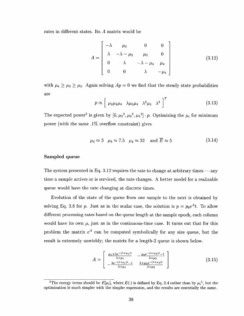
3-4 Minimum power vs. sample time . .................. . 39
4-1 Feedback loops around the power supply vs. the system ....... . 42
4-2 Linear regulator ............ ......... ....... .. 43
4-3 Switched-capacitor converter ................... .... 44
4-4 Simplified buck converter schematic . .................. 45
4-5 Passive damping ........................... 46
4-6 Active damping ................. ............ 47
4-7 Active damping waveforms ......... . . . . . ......... .. 48
4-8 Open-loop variable supply system ................... . 48
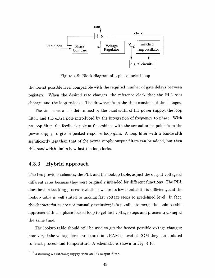
4-9 Block diagram of a phase-locked loop . ................. 49
4-10 Hybrid system ............................... 50
4-11 Quantization effect ................. ......... 51
5-1 Dynamic supply voltage chip block diagram . ............. 54
5-2 FIFO block diagram ........................... 55
5-3 Rate translation block diagram ................... .. 56
5-4 PW M block diagram ........................... 58
5-5 Ring oscillator block diagram ................... . . . . . . 59
5-6 DSP block diagram ............................ 60
5-7 Variable supply controller chip plot . .................. 61
5-8 Initial results .. .. . .. .. . .. ..... . . . . . . . .... .. . 62
6-1 Parasitic losses in buck converter ................... . 64
A-1 Top level schematics ........................... 70
A-2 FIFO buffer ................................ 71
A-3 Power supply controller schematics . .................. 72
A-4 Pulse width modulator .......................... 73
A-5 Signal processing and delay chains ................... . 74
A-6 Ring oscillator . .................. ............ 75
A-7 Synchronization block .......................... 76
Chapter 1
Overview of Low Power ICs
In the last several years power consumption of integrated circuits has become an
increasingly important design constraint. One reason has been the demand for longer
battery life from portable electronics applications like laptop computers and mobile
phones; control of power consumption has proved to be a more significant factor than
battery technology for increasing run-time. Another factor has been the the increasing
power density of microprocessors; the package and circuit board have to dissipate the
30W of heat that a Dec Alpha 21164 or Pentium Pro processor generates.
1.1 Low power hierarchy
Power dissipation in CMOS circuits is proportional to the switched capacitance and
the supply voltage squared; a reduction in either will lead to power savings. Not
surprisingly, a wide variety of methods to lower power have been investigated. These
can broadly classified by level of abstraction: technology, circuit design, architecture,
and algorithm [5].
1.1.1 Technology
From the standpoint of system design the term "technology" includes everything
from device doping levels to layout design rules to packaging. Some of the most
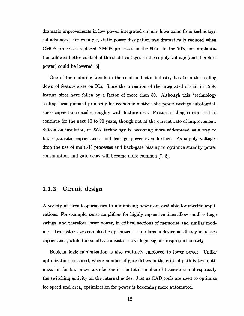
dramatic improvements in low power integrated circuits have come from technologi-
cal advances. For example, static power dissipation was dramatically reduced when
CMOS processes replaced NMOS processes in the 60's. In the 70's, ion implanta-
tion allowed better control of threshold voltages so the supply voltage (and therefore
power) could be lowered [6].
One of the enduring trends in the semiconductor industry has been the scaling
down of feature sizes on ICs. Since the invention of the integrated circuit in 1958,
feature sizes have fallen by a factor of more than 50. Although this "technology
scaling" was pursued primarily for economic motives the power savings substantial,
since capacitance scales roughly with feature size. Feature scaling is expected to
continue for the next 10 to 20 years, though not at the current rate of improvement.
Silicon on insulator, or SOI technology is becoming more widespread as a way to
lower parasitic capacitances and leakage power even further. As supply voltages
drop the use of multi-Vt processes and back-gate biasing to optimize standby power
consumption and gate delay will become more common [7, 8].
1.1.2 Circuit design
A variety of circuit approaches to minimizing power are available for specific appli-
cations. For example, sense amplifiers for highly capacitive lines allow small voltage
swings, and therefore lower power, in critical sections of memories and similar mod-
ules. Transistor sizes can also be optimized - too large a device needlessly increases
capacitance, while too small a transistor slows logic signals disproportionately.
Boolean logic minimization is also routinely employed to lower power. Unlike
optimization for speed, where number of gate delays in the critical path is key, opti-
mization for low power also factors in the total number of transistors and especially
the switching activity on the internal nodes. Just as CAD tools are used to optimize
for speed and area, optimization for power is becoming more automated.
1.1.3 Architecture
A large fraction of current research in low power is aimed at optimizing circuit ar-
chitectures. Pipelining and parallelization are mainstay techniques in microprocessor
design, but many other architecture decisions affect power as well. In the case of
microprocessors, the size and access frequency of the instruction and data caches, the
number of registers, clock distribution, the number of busses, and even the instruction
set affects power performance.
Even more issues come up in DSP design. Number representation, for example, is
the focus of some discussion. Is sign & magnitude or one-hot coding better than two's
complement? Some of the other issues include the use of parallel vs. time-multiplexed
resources, chain vs. tree arithmetic structures, synchronous vs. asynchronous design,
etc. The tradeoff between power, speed, and area is explicit in architecture design.
1.1.4 Algorithm
The premise behind algorithmic optimization is so intuitive as to rarely be stated
explicitly: simpler algorithms require smaller, lower power circuits. One of the most
familiar and oldest examples of algorithmic optimization is the Fast Fourier trans-
form. Direct computation of a length-N Discrete Time Fourier Transform takes N 2
operations; an FFT computes the same result in only Nlog 2N. For a modest 512
element transform, that corresponds to 50-fold reduction in the number operations. A
system that implements an FFT could tolerate longer gate delays and a lower voltage
than one the computes the DTFT directly if the total processing time is fixed.
The biggest drawback to optimization at the algorithmic level is that the solutions
are specific to very closely related problems; the FFT can be modified to compute
a discrete cosine transform, for example, but contributes nothing to microcode exe-
cution or factoring integers. On the other hand, algorithm improvements are readily
transferred to new technologies and circuit styles.

1.2 Dynamic optimization
The common thread through these techniques is that the optimization for low power
is static; that is, whatever parameter is being optimized, be it supply voltage or circuit
layout or state-assignment in an finite state machine, is optimized for low power at
design time. In fact, in some applications optimizing the circuit during operation
could save more power.
A handful of methods exist for optimizing circuit performance at run time; adap-
tive filters adjust the coefficients of their taps as data comes in, for example. And
power down techniques strive to eliminate power consumption of idle blocks. How-
ever, in almost all cases the power supply is treated as a fixed voltage, and the clock
as a fixed frequency.' In fact, the system clock and supply voltage can also be ad-
justed dynamically to lower overall system power. This optimization is the focus of
this thesis.
1.3 Previous work on variable power supplies
A key previous work on variable power supplies involves compensating process and
temperature variations by adjusting the power supply. Since threshold voltages can-
not be controlled precisely, conventional ICs are designed to work under worst-case
conditions. If actual circuit delays could be measured, the supply voltage could be
lowered until the actual circuit delays match the maximum allowed delays. This idea
can be carried further by using self-timed circuits where global clocks are eliminated
completely and local handshaking establishes timing; both approaches are described
below.
1Adiabatic logic families have AC rather than DC power supplies, but the power waveform is stillprescribed at design time.
1.3.1 Dynamic process compensation
Several systems have been designed to compensate for process and temperature vari-
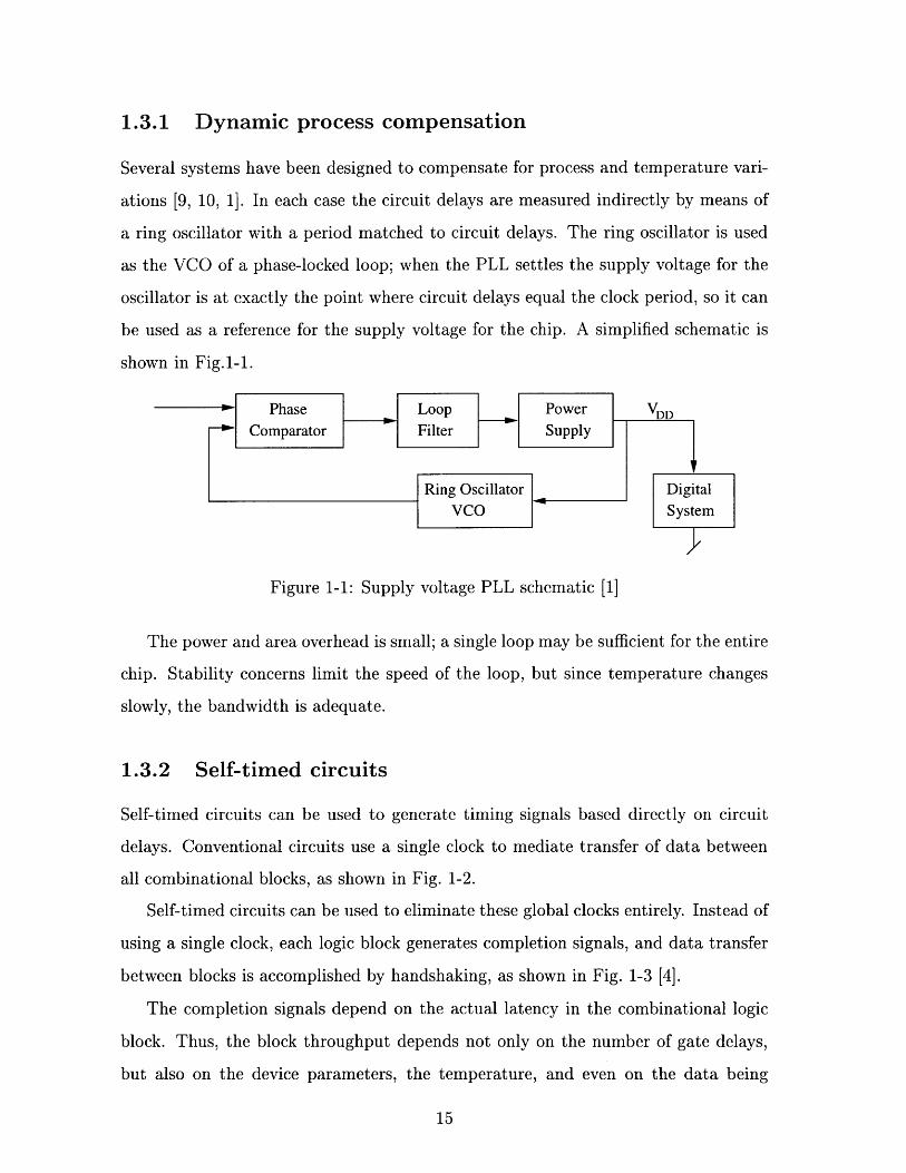
ations [9, 10, 1]. In each case the circuit delays are measured indirectly by means of
a ring oscillator with a period matched to circuit delays. The ring oscillator is used
as the VCO of a phase-locked loop; when the PLL settles the supply voltage for the
oscillator is at exactly the point where circuit delays equal the clock period, so it can
be used as a reference for the supply voltage for the chip. A simplified schematic is
shown in Fig.1-1.
Figure 1-1: Supply voltage PLL schematic [1]
The power and area overhead is small; a single loop may be sufficient for the entire
chip. Stability concerns limit the speed of the loop, but since temperature changes
slowly, the bandwidth is adequate.
1.3.2 Self-timed circuits
Self-timed circuits can be used to generate timing signals based directly on circuit
delays. Conventional circuits use a single clock to mediate transfer of data between
all combinational blocks, as shown in Fig. 1-2.
Self-timed circuits can be used to eliminate these global clocks entirely. Instead of
using a single clock, each logic block generates completion signals, and data transfer
between blocks is accomplished by handshaking, as shown in Fig. 1-3 [4].
The completion signals depend on the actual latency in the combinational logic
block. Thus, the block throughput depends not only on the number of gate delays,
but also on the device parameters, the temperature, and even on the data being

Figure 1-2: Global clocks
Figure 1-3: Local timing generation
processed at a bit level. This has been observed to give widely varying computation
times for different data [4, 2].
Just as in the case of synchronous systems, the supply voltage can be lowered to
save power until the throughput just meets system requirements. A small self-timed,
variable voltage supply has been demonstrated by Nielssen et. al. [2]. The system,
diagrammed in Fig. 1-4, consists of two FIFO buffers, a self-timed 16-bit ripple-carry
Synchronous
Figure 1-4: Self-timed system diagram [2]
adder and a D/A driving a power supply. The length of the ripple-carry propagation
affects how long each addition takes. By monitoring the number of elements in the
input queue the system automatically determines whether the processing is too fast
or too slow and adjusts the supply voltage accordingly.
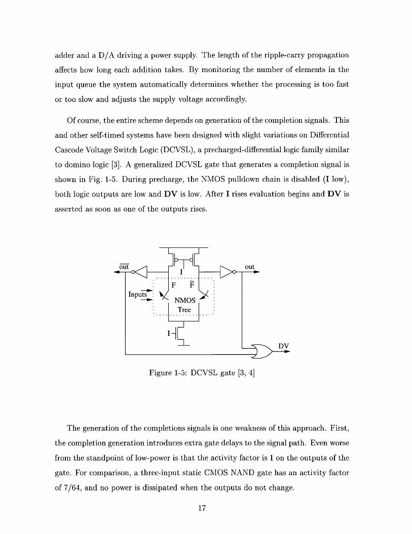
Of course, the entire scheme depends on generation of the completion signals. This
and other self-timed systems have been designed with slight variations on Differential
Cascode Voltage Switch Logic (DCVSL), a precharged-differential logic family similar
to domino logic [3]. A generalized DCVSL gate that generates a completion signal is
shown in Fig. 1-5. During precharge, the NMOS pulldown chain is disabled (I low),
both logic outputs are low and DV is low. After I rises evaluation begins and DV is
asserted as soon as one of the outputs rises.
Figure 1-5: DCVSL gate [3, 4]
The generation of the completions signals is one weakness of this approach. First,
the completion generation introduces extra gate delays to the signal path. Even worse
from the standpoint of low-power is that the activity factor is 1 on the outputs of the
gate. For comparison, a three-input static CMOS NAND gate has an activity factor
of 7/64, and no power is dissipated when the outputs do not change.
1.4 Thesis focus
There is no way to exploit the bit-level data dependencies without resorting to a self-
timed system. However, in many applications the processing requirements change
at an algorithmic level, and these variations can be exploited by any synchronous
system.
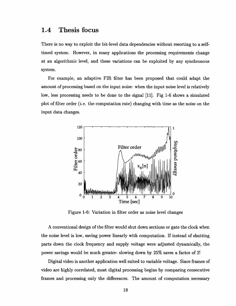
For example, an adaptive FIR filter has been proposed that could adapt the
amount of processing based on the input noise: when the input noise level is relatively
low, less processing needs to be done to the signal [11]. Fig 1-6 shows a simulated
plot of filter order (i.e. the computation rate) changing with time as the noise on the
input data changes.
120
100
80;--o
6060
40
20
n
1
CD
0V0 1 2 3 4 5 6 7 8 9 10
Time [sec]
Figure 1-6: Variation in filter order as noise level changes
A conventional design of the filter would shut down sections or gate the clock when
the noise level is low, saving power linearly with computation. If instead of shutting
parts down the clock frequency and supply voltage were adjusted dynamically, the
power savings would be much greater- slowing down by 25% saves a factor of 2!
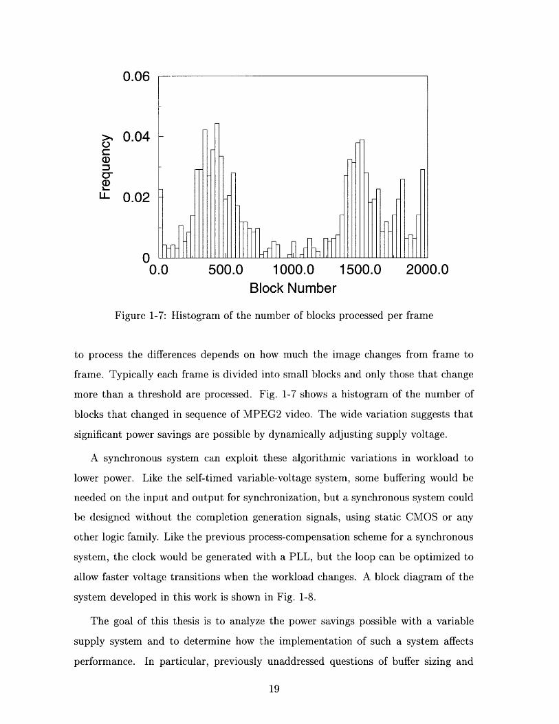
Digital video is another application well suited to variable voltage. Since frames of
video are highly correlated, most digital processing begins by comparing consecutive
frames and processing only the differences. The amount of computation necessary
,' ~~r'U.UO
>, 0.040
LL 0.02
17 U0.0 500.0 1000.0 1500.0 2000.0
Block Number
Figure 1-7: Histogram of the number of blocks processed per frame
to process the differences depends on how much the image changes from frame to
frame. Typically each frame is divided into small blocks and only those that change
more than a threshold are processed. Fig. 1-7 shows a histogram of the number of
blocks that changed in sequence of MPEG2 video. The wide variation suggests that
significant power savings are possible by dynamically adjusting supply voltage.
A synchronous system can exploit these algorithmic variations in workload to
lower power. Like the self-timed variable-voltage system, some buffering would be
needed on the input and output for synchronization, but a synchronous system could
be designed without the completion generation signals, using static CMOS or any
other logic family. Like the previous process-compensation scheme for a synchronous
system, the clock would be generated with a PLL, but the loop can be optimized to
allow faster voltage transitions when the workload changes. A block diagram of the
system developed in this work is shown in Fig. 1-8.
The goal of this thesis is to analyze the power savings possible with a variable
supply system and to determine how the implementation of such a system affects
performance. In particular, previously unaddressed questions of buffer sizing and
7miJKl l l II I I 1 I 1
;i L1II I I I I I I I I I I i II I II I I I 1 I l I I
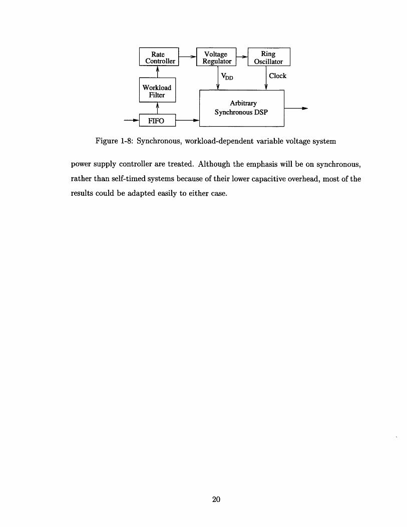
Figure 1-8: Synchronous, workload-dependent variable voltage system
power supply controller are treated. Although the emphasis will be on synchronous,
rather than self-timed systems because of their lower capacitive overhead, most of the
results could be adapted easily to either case.
Chapter 2
Variable Supply Fundamentals
Since the goal of a variable supply system is to minimize power, it is best to start by
considering what sets the power dissipation of a digital system. If both the technology
and architecture are fixed, the determining factor in power dissipation is timing: at
higher voltages, the circuits operate faster but burn more power. The analysis begins
by deriving the relationship of dissipated power to processing speed.
2.1 First order derivation
A convenient formalism is that digital signal processing deals with data as discrete
samples. A sample may be as small as 12 bits in the case of audio processing or
as large as a 1,000,000 bits for a full frame of video, but the data always comes in
discrete chunks. In most cases the samples come at a fixed frequency; hence, the
average power and computation for the processor can be related to the energy per
sample and the computation performed therein.
In CMOS circuits most of the power goes to charging and discharging capacitances,
so a starting approximation for the energy per sample is
E = nCVDD (2.1)
where n is the number of clock cycles per sample time, C is the average switched
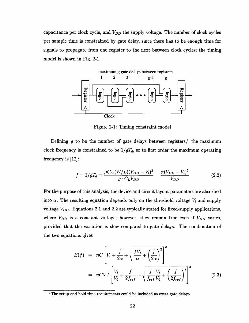
capacitance per clock cycle, and VDD the supply voltage. The number of clock cycles
per sample time is constrained by gate delay, since there has to be enough time for
signals to propagate from one register to the next between clock cycles; the timing
model is shown in Fig. 2-1.
maximum g gate delays between registers1 2 3 g-1 g
Figure 2-1: Timing constraint model
Defining g to be the number of gate delays between registers,1 the maximum
clock frequency is constrained to be 1/gTd, so to first order the maximum operating
frequency is [12]:
f = 1/gTd = Co(W/L)(VDD - t)2 (VDD - Vt) 2 (2.2)g - CLVDD VD ooD
For the purpose of this analysis, the device and circuit layout parameters are absorbed
into a. The resulting equation depends only on the threshold voltage Vt and supply
voltage VDD. Equations 2.1 and 2.2 are typically stated for fixed-supply applications,
where VDD is a constant voltage; however, they remain true even if VDD varies,
provided that the variation is slow compared to gate delays. The combination of
the two equations gives
f fVt f 2 2E ( f ) = nC Vt + -+ f- ( + )2
2a a 2a2
Vt f f )2= nCV0 + + - + (2.3)
The setup and hold time requirements could be included as extra gate delays.fef fef V
'The setup and hold time requirements could be included as extra gate delays.

where Vo = fref//a = (Vref - Vt) 2 /Vref and Vref is a reference supply voltage. Since
the sample time is fixed, the clock frequency determines how many operations are
performed per sample. If T, is the sample time, the number of clock cycles is given
by n = fT,, and Eq. 2.3 can be rewritten as
Vt f f VtE(f) = CVo2 T fT 8 2
E(r)= E + r/2 + r-+ (r/2)2 (2.4)
where E 0 is a scaling factor with units of energy and r = f/fref is the normalized
sample processing rate, or simply rate. Here fre, is the frequency of operation at
VDD = Vref, so if Vre1 is the highest available voltage, fref is the maximum achievable
frequency and r is normalized to 0 < r < 1.
Eq. 2.4 can be used to estimate how power dissipation varies with processing
rate. For example, if a frame of video requires half the maximum computation, the
clock speed could be halved and voltage lowered to cut power by a factor of four:
E(.5) = .22 x E(1).Conventional digital logic works at a fixed voltage and idles if the computation
finishes early. The comparable equation to Eq. 2.4 for fixed voltage is Efized(r) =
E(1)r, because the energy per operation is constant and only the number of operations
changes; the clock can be gated to avoid dissipating power once data processing has
finished. So, to process the same half-frame of video, a fixed-voltage system uses
1/2 the energy it would take for a full frame, more than twice as much as a variable
supply system!
Fig. 2-2 shows a plot of Eq. 2.4, for Vref = VDDmax = 2V and Vt = .4V alongE(r)
with the fixed-supply line. The ratio of the two curves - E(1)r gives the energy
savings ratio per block for any given r, but the ratio changes with r. At high rates
the power is the same because the voltage is the same; at very low rates the variable
voltage approaches Vt, so the ratio approaches is ( V ) . The area between the
curves is a convenient measure of the energy savings achievable by varying supply

1.0
0.8
> 0.6
W 0.4
0.2
n0n
0.0 0.2 0.4 0.6 0.8 1.0Rate
Figure 2-2: Energy vs. rate for variable and fixed supply systems
voltage without assuming a specific rate.
2.2 Second order corrections
2.2.1 Velocity saturation
One of the implicit assumptions made in deriving Eq. 2.2 was that the drift velocity of
electrons in the channel is small compared to their thermal velocity. This corresponds
to a VDS much less than 1V per micron of channel length; for comparison, a digital
circuit may have a 2V power supply and .3[/m channel lengths, so a different model
is needed to predict device behavior [13]. A precise calculation of velocity saturation
influence on gate delay is messy [14], but a qualitative modification to Eq. 2.2 will
suffice:
a(VDD - V()2f (= (2.5)VDD(1 + VDD/Vs)
Vs is the "corner voltage" at which velocity saturation effects limit the output current
to half the value it would have been without the short channel effect. The extra
factor has the desired effect of lowering the the speed at supply voltages higher than
Vs without affecting performance at low voltages.
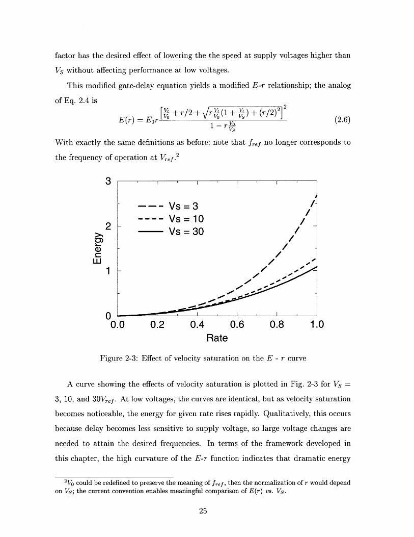
This modified gate-delay equation yields a modified E-r relationship; the analog
of Eq. 2.4 is
±r + r/2 + VrT(1 + -t) + (r/2)-]E(r) = Eor 1
Vs
(2.6)
With exactly the same definitions as before; note that fref no longer corresponds to
the frequency of operation at Vref. 2
3
2C:
a)u-
n0.0 0.2 0.4 0.6 0.8 1.0
Rate
Figure 2-3: Effect of velocity saturation on the E - r curve
A curve showing the effects of velocity saturation is plotted in Fig. 2-3 for Vs =
3, 10, and 3 0 Vr,,f. At low voltages, the curves are identical, but as velocity saturation
becomes noticeable, the energy for given rate rises rapidly. Qualitatively, this occurs
because delay becomes less sensitive to supply voltage, so large voltage changes are
needed to attain the desired frequencies. In terms of the framework developed in
this chapter, the high curvature of the E-r function indicates that dramatic energy
2Vo could be redefined to preserve the meaning of fref, then the normalization of r would dependon Vs; the current convention enables meaningful comparison of E(r) vs. Vs.
T~r I rr . . . .0~

savings are possible by scaling voltage, either statically by changing the architecture,
or dynamically.
2.2.2 Leakage
Equation 2.1 does not describe all the power dissipation in ICs. One correction term,
for example, is the power loss due to short-circuit currents during switching. For the
sake of this discussion that term can be lumped into 2.1 by increasing C slightly, and
the analysis remains essentially the same. On the other hand, power dissipation due
to sub-threshold conduction is fundamentally different.
This leakage current adds a term to the DC power consumption that depends
linearly on VDD but exponentially on Vt:
Psubthreshold OC VDD e -Vt/nVT (2.7)
where VT = kT/q is the thermal voltage and n is a non-ideality factor approximately
equal to 2 for MOSFETS. As supply voltages scale down, threshold voltages scale
down as well and leakage becomes a significant fraction of the total power [7]. Fol-
lowing the logic of the first section, it may well save power by slowing down - but
slow down by raising Vt instead of lowering VDD. Fig 2-4 shows the similarity between
the methods.
Figure 2-4: Raising Vt vs. lowering VDD
The numbers bear this out: take a 1.2V supply voltage with .3V Vt, and assume
that the activity is such that leakage contributes 30% to total power. Raising Vt by
50mV slows the circuit down by about 10%, and cuts the total power by .30 x (1 -
e- 50 /(2-26)) + .1 x .7 , 26% which counts the 7% savings for doing fewer operations
and the rest for the reduction in leakage. For comparison, varying VDD for the same
speed reduction gives only about 15% lower power.
Leakage power will not be addressed specifically in the rest of the thesis. However,
almost all of the results derived for variably VDD apply equally well to variable Vt.
When this component of the power becomes significant, variable bulk biasing will be
one way to lower power.
2.3 Parallelization
The plot of energy versus rate is a convenient tool to use to analyze the influence of
different architectures on power. In particular, the effect of parallelization is easy to
show. The idea is to copy a circuit block N times and divide the system clock by N;
since the clock slows down, the voltage can be lowered, and the system runs at lower
power. Algebraicly, the parallel system has an energy - rate relation given by
Epar (r; N) = (1 + k)NE(r/N) (2.8)
where the (l+k) accounts for overhead associated with parallelization. This overhead
can be substantial, though the discussion is outside the scope of this thesis; k = 0 will
be assumed. Fig. 2-5 shows an E-r plot of Eq. 2.8 for N = 1 (the reference system)
and for N = 2 and 16, again with the fixed-supply lines for comparison.
There are two important to be made from the plot. First, increasing parallelization
lowers energy for all rates (again assuming k = 0). The second is that the E-r
curve has a smaller curvature for the higher Ns. Equivalently, the area between the
constant supply and variable supply curves is relatively smaller, so the power savings
achievable by varying voltage diminish for higher Ns. This is exactly the same effect
that limits the energy savings from further parallelization: in both cases the energy
savings arise because energy per clock cycle increases with speed. As VDD approaches
Vt circuit delay increases rapidly, so slowing the clock allows only small changes in

C1m
1.0
0.8
0.6
0.4
0.2
n nV.V0.0 0.2 0.4 0.6 0.8 1.0
Rate
Figure 2-5: Effect of parallelization on power
VDD, and if voltage doesn't change, the energy per clock cycle doesn't change with
rate. Mathematically, this result comes naturally from Eq. 2.8:
Ev,,r(r; N) = NE(r/N)
= Eor[ + r/2N + r/NO +(r/2N)rIV+ (r/2N)2] (2.9)
and taking the limit as N goes to infinity gives
lim Epar(r; N) = CfrefTorVt2N-oo
(2.10)
which is the expected minimum. In fact, because of subthreshold conduction Eq. 2.4
does not model device performance correctly if VDD approaches Vt. However, gate
delays increase so rapidly near the threshold voltage that Eq. 2.10 is nearly correct.
Chapter 3
Rate Control
The equations in the previous chapter define the static relationship between power
and processing rate; in other words, the instantaneous power as a function of rate.
The dynamic behavior, or the average power as a function of a sequence of rates, is
equally important.
3.1 Averaging rate
There is a subtle but significant distinction between the processing rate r and what
will be called the computational workload, denoted w. The rate r is the processing
speed, or more simply the system clock frequency, while w is a measure of how
much processing needs to be done on the incoming blocks of data. For example, a
digital video application may have a maximum clock rate of 50MHz and computation
dependent on what fraction of the image changed. Half of the image changing on a
certain frame corresponds to w = 1/2. If the clock frequency happens to be 30MHz
during the computation of that frame, r = .6; as long as both r and w are normalized,
the computation on that sample will finish for r > w. Even in the cases where it
is not necessary, it is often advantageous to buffer the workload so that r need not
follow w exactly. Why incur the overhead of a buffer when r can be set equal to w?
3.1.1 Motivation
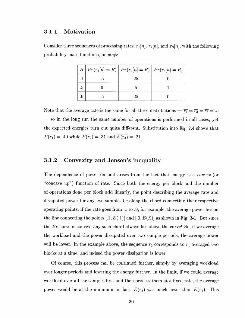
Consider three sequences of processing rates, rl[n], r2 [n], and r3 [n], with the following
probability mass functions, or pmfs:
Note that the average rate is the same for all three distributions - r- = - = 7 = .5
so in the long run the same number of operations is performed in all cases, yet
the expected energies turn out quite different. Substitution into Eq. 2.4 shows that
E(rl) = .40 while E(r 2) = .31 and E(r 3) = .21.
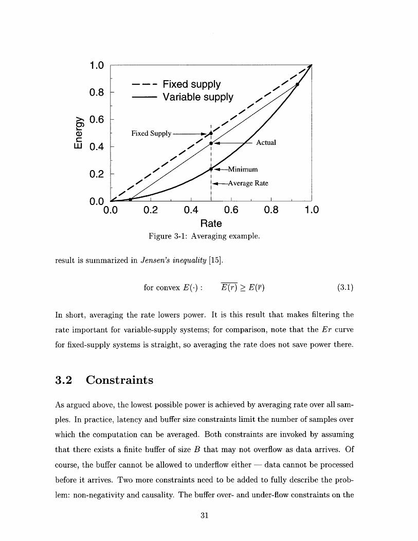
3.1.2 Convexity and Jensen's inequality
The dependence of power on pmf arises from the fact that energy is a convex (or
t"concave up") function of rate. Since both the energy per block and the number
of operations done per block add linearly, the point describing the average rate and
dissipated power for any two samples lie along the chord connecting their respective
operating points; if the rate goes from .1 to .9, for example, the average power lies on
the line connecting the points [.1, E(.1)] and [.9, E(.9)] as shown in Fig. 3-1. But since
the Er curve is convex, any such chord always lies above the curve! So, if we average
the workload and the power dissipated over two sample periods, the average power
will be lower. In the example above, the sequence r2 corresponds to rl averaged two
blocks at a time, and indeed the power dissipation is lower.
Of course, this process can be continued further, simply by averaging workload
over longer periods and lowering the energy further. In the limit, if we could average
workload over all the samples first and then process them at a fixed rate, the average
power would be at the minimum; in fact, E(r 3) was much lower than E(ri). This
R Pr(rl[n] = R) Pr(r2[n] = R) Pr(r3[n] = R)
.1 .5 .25 0
.5 0 .5 1
.9 .5 .25 0
4
I.U
0.8
> 0.6C,
W 0.4
0.2
n n0.0 0.2 0.4 0.6 0.8 1.0
RateFigure 3-1: Averaging example.
result is summarized in Jensen's inequality [15].
for convex E(.) : E(r) > E(T) (3.1)
In short, averaging the rate lowers power. It is this result that makes filtering the
rate important for variable-supply systems; for comparison, note that the Er curve
for fixed-supply systems is straight, so averaging the rate does not save power there.
3.2 Constraints
As argued above, the lowest possible power is achieved by averaging rate over all sam-
ples. In practice, latency and buffer size constraints limit the number of samples over
which the computation can be averaged. Both constraints are invoked by assuming
that there exists a finite buffer of size B that may not overflow as data arrives. Of
course, the buffer cannot be allowed to underflow either - data cannot be processed
before it arrives. Two more constraints need to be added to fully describe the prob-
lem: non-negativity and causality. The buffer over- and under-flow constraints on the
rate r[n] given a workload w[n] are
no no no-B
Vno: E w[n] EZ r[n] w[n] (3.2)n=--oo n=-oo n=-oo
The left inequality guarantees that no more data is processed than has arrived, i.e.
that the buffer cannot underflow. The right one has the complementary role: to
guarantee that all data that arrived B or more samples ago has been processed; that
is, the buffer cannot overflow. Of course, in the long run, the average rate and the
average processing load must be equal. This is consistent with the limits as stated;
dividing the inequalities in Eq. 3.2 by 1/no and taking the limit' as no goes to infinity
gives r[n] = w[n].
As described by the constraints in Eq. 3.2, the optimum r[n] depends on the pmf
of the workload. Even for simple distributions the optimization rapidly becomes un-
manageable. Furthermore, even when a functional form exists, the calculation of r[n]
from a w [n] sequence could be prohibitive in terms of area and power. Fortunately,
approximations exist.
FIR filter of the workload
A moving average of the workload is a simple, good approximation to r[n]. It can be
shown that any weighted average satisfies the required constraints for any w[n]. This
average can be written as an FIR filter with constraints as shown below in Eq. 3.2.
B-1
r[n] = E akw[n - k] (3.3)k=0
0 < ak 1 a = 1 (3.4)
The filter is causal by construction. It is also conveniently time-invariant and linear.
Non-negativity of r[n] is guaranteed by choosing the ak as prescribed in Eq. 3.4. That
1It is possible to come up with pathological distributions for w[n] that have no mean. Eq. 3.2could be rewritten in terms of finite moving averages to fix this problem. However, the problem issufficiently obscure in this context that it will be ignored.
this satisfies the over- and under-flow constraints is shown below.
FIR mechanics
Before starting the proof, the difference between the workload in the FIR and the
sample in the input buffer should be stressed. The data samples in the input buffer
are processed at varying speeds depending on the current value of r. Sometimes more
than one sample is finished per sample period, sometimes less; the number of data
samples in the input buffer (i.e. the frames of video or digitized speech or whatever
else) varies with time. On the other hand, the FIR filter performs a weighted average
of the workload of the last B data samples, whether or not they have already gone
through the DSP.
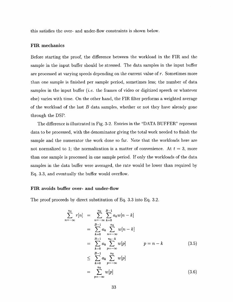
The difference is illustrated in Fig. 3-2. Entries in the "DATA BUFFER" represent
data to be processed, with the denominator giving the total work needed to finish the
sample and the numerator the work done so far. Note that the workloads here are
not normalized to 1; the normalization is a matter of convenience. At t = 3, more
than one sample is processed in one sample period. If only the workloads of the data
samples in the data buffer were averaged, the rate would be lower than required by
Eq. 3.3, and eventually the buffer would overflow.
FIR avoids buffer over- and under-flow
The proof proceeds by direct substitution of Eq. 3.3 into Eq. 3.2.
no no B-1
Sr[[n] = • akw[n-- k]n=-oo n=-oo k=0O
B-1 no
-Zak Z w[n-k]k=O n=-oo
B-1 no-k
S ak E p] p =n - k (3.5)k=O p=-oo
B-1 no
< Z ak Z w[p]k=O p=-oo
no
= E w[p] (3.6)p=-oo

Workload: 6,3,21,12,27,9,...
Notation: done/total
DATA BUFFERWorkload FIR
t=0
t=1
t=2
0/6
0/3
0/21
0 0 6 0 oo10 Avg=2
2/6 0 13 6 Avg=3
0/3 5/6 213 16 Avg=10
0/12 15/21 1122113 Avg=12
0/27 8/12 27 12 21 Avg=20
L9 27 12 Avg=16n/ 1/1'7 9 1271121Ag6
Figure 3-2: FIR mechanics
The inequality shows that the buffer cannot underflow, and a similar sequence shows
that it cannot overflow. Starting from Eq. 3.5 gives the following result:
B-1 no-k
= ak E w[p]k=O p=-oo
B-1 no-B
> E ak E w[p]k=O p=-oo
no-B
- w [p]p=-oo
p=n-k
(3.7)
Which completes the proof. Intuitively, the buffers do not overflow because the system
is linear and any single data sample is processed correctly. That is, if only one
data sample required computation and all the others were zero, by the Bth sample
t=3
t=4
t=5
no
r [n]n=-oo
·
I i I I
' ' '
V17 IVILI
I
........
7
.... .. .............................-- - - - - - -
time, exactly enough operations would have been completed to finish processing that
sample. Since the r[n] superpose, the system satisfies the processing constraints for
all the data samples.
3.3 Update rate
It is clear that data buffers allow r to be somewhat decoupled from w; as shown
above, the rate can be averaged over several samples to lower power. It is a small
step to push the buffering idea further: if the power (and hence the rate) are averaged
over B samples, shouldn't we only have to update r at 1/B of the sample frequency?
As shown in chapter 4, slowing the update rate can save power in the power supply.
Unfortunately, this can have unwelcome repercussions in the power dissipated in the
DSP. Two examples are analyzed below: a subsampled FIR controller and quasi-
Poisson queue.
3.3.1 Subsampled FIR
Fig. 3-3 compares the processing rates on a sample w[n] sequence achieved by two
B = 2 controllers: system A updates on every sample, while system B updates on
every other sample. Label the workload of the data sitting in the ith position of the
input buffer wi. By setting the rate equal to the average workload in the buffer -
r - ww- system A never idles, and at the same time guarantees that a there
is always room in the buffer for the next data sample when it arrives. This is a
specialization of the "weighted average FIR" controller analyzed above.
The added constraint on system B appears when wl > w2, which happens in the
example at t = 4. If the system works at the average rate, the first element will not
be out of the queue before the next data sample arrives. In fact, to guarantee that
the queue does not overflow the rate controller has to work at r = max(wl, w+2W).
In order to work at the average rate, system B would need a buffer of length 3. This
extra buffering is needed by any system that slows down the update rate; in order
to update at 1/C of the sample arrival time, the buffer length is constrained to be

System A
t=00o o
rate=O
t=10/4 0
rate=2
t=20/8 2/4
rate=6
t=30/6 4/8
rate=7
t=40/2 3/6
rate=4
J•l , •
Figure 3-3: Rate averaging example
B > 2C - 1.
3.3.2 Quasi-Poisson queues
Poisson queues, or queues with exponentially distributed service and arrival times,
may be used to model a variety of physical process, including some signal processing
applications. For example, a packet-switched network may be modeled as a Poisson
queue: the packets arrive independently, and are decoded and routed faster if they
have fewer errors. We may be interested in finding the processing rate at which the
probability PL of losing packets due to buffer overflow is less that some constant.
This problem is easily solved as follows.
System B
0 0i rate=0
0/4 0
i rate=6
0/6 2/8
0/2 0/6rate = 4 ?. _ o
Poisson queue solution
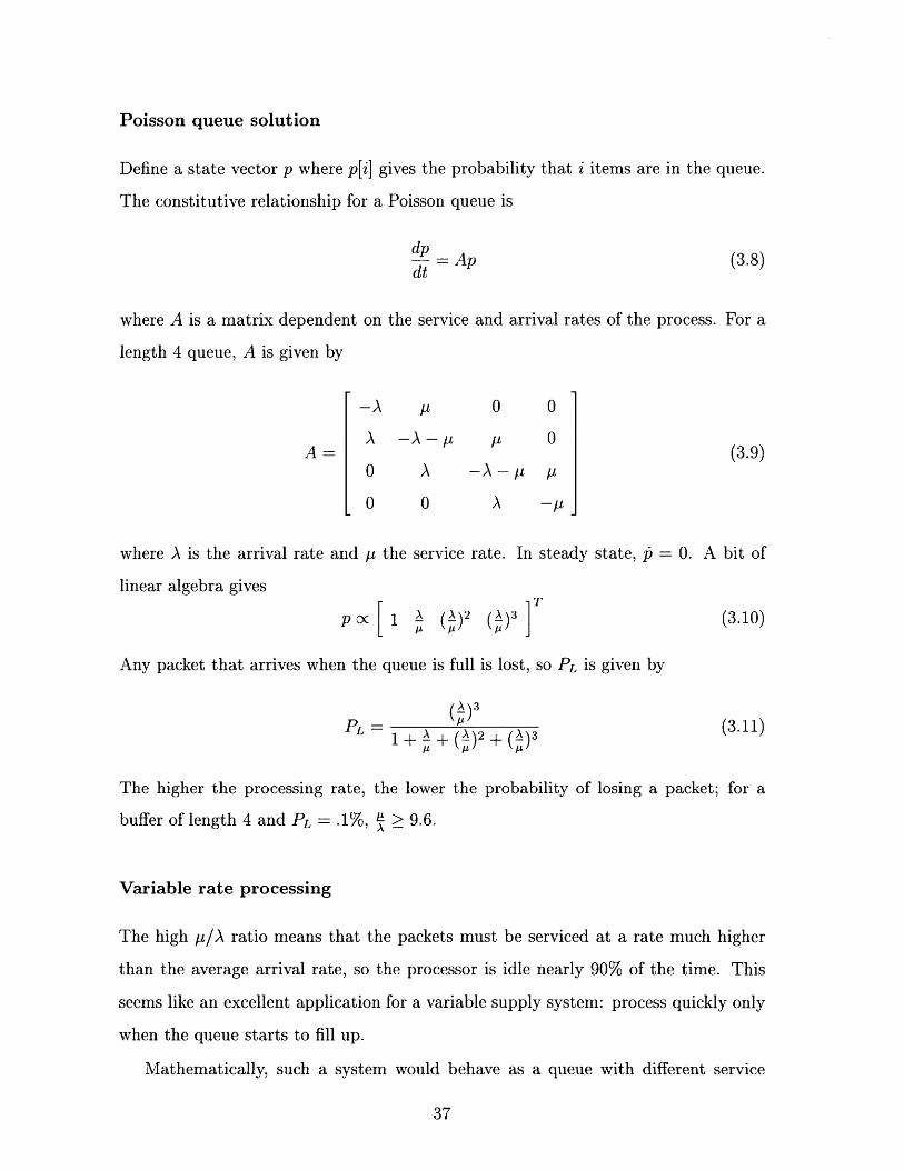
Define a state vector p where p[i] gives the probability that i items are in the queue.
The constitutive relationship for a Poisson queue is
dp= Ap
dt(3.8)
where A is a matrix dependent on the service and arrival
length 4 queue, A is given by
-A
A
0
0
P
-A -p
A
0
0
A-
A
0
0
P-P-IIL
rates of the process. For a
(3.9)
where A is the arrival rate and p the service
linear algebra gives
rate. In steady state, i5 = 0. A bit of
p o 1 A )2
Any packet that arrives when the queue is full is lost, so PL is given by
PL= -1+ + (A)2 + (A)3A IL A)
(3.10)
(3.11)
The higher the processing rate, the lower the probability of losing a packet; for a
buffer of length 4 and PL = .1%, - > 9.6.
Variable rate processing
The high p/A ratio means that the packets must be serviced at a rate much higher
than the average arrival rate, so the processor is idle nearly 90% of the time. This
seems like an excellent application for a variable supply system: process quickly only
when the queue starts to fill up.
Mathematically, such a system would behave as a queue with different service
rates in different states. Its A matrix would be
-A P2 0 0
A -A- [ 2 13 0
0 A -AX- p 3 14
0 0 A -114
(3.12)
with P/4 Ž P3 Ž P2. Again solving Ap = 0 we find that the steady state probabilities
are
p C [ 213P4 A/13/34 A2p 4 A3 (3.13)
The expected power 2 is given by [0, p22, P32, P42] . p. Optimizing the pi for minimum
power (with the same .1% overflow constraint) gives
p/2 3 p13-7.5 p4 32 and E 5 (3.14)
Sampled queue
The system presented in Eq. 3.12 requires the rate to change at arbitrary times - any
time a sample arrives or is serviced, the rate changes. A better model for a realizable
queue would have the rate changing at discrete times.
Evolution of the state of the queue from one sample to the next is obtained by
solving Eq. 3.8 for p. Just as in the scalar case, the solution is p = poeAt. To allow
different processing rates based on the queue length at the sample epoch, each column
would have its own p, just as in the continuous-time case. It turns out that for this
problem the matrix eA can be computed symbolically for any size queue, but the
result is extremely unwieldy; the matrix for a length-2 queue is shown below.
A = - 12 (3.15)Ae-(A+1l)t--1 A+±, 2 e-(-X+/2)t
A+p1 A+P2
2 The energy terms should be E[pi], where E(-) is defined by Eq. 2.4 rather than by pi2 , but theoptimization is much simpler with the simpler expression, and the results are essentially the same.
A =
It becomes extremely difficult to optimize the rates symbolically for even a very
small queue, so an approximate solution was obtained numerically. The minimum
power solution for the length 4, .1% overflow case is plotted in Fig. 3-4 for a range of
sample times.
10
9
Sample Time / Arrival Rate
Figure 3-4: Minimum power vs. sample time
For update times much faster than the arrival rate, the minimum power solution
approaches the unconstrained minimum of Eq. 3.14. For times much slower than
the arrival rate, the system cannot vary the rate as fast as the queue fills up, so the
minimum is simply the fixed-rate minimum. The key observation is that for supply
voltage variation to be effective, the voltage update time must be comparable to the
workload variation time. In other words, the bandwidth of the power supply must
exceed the rate at which data arrives.
J A

Chapter 4
Variable Supply and Clock
Generation
In variable supply systems, power savings are achieved by lowering the supply voltage
as the system clock slows down; indeed, this is the only reason such a system saves
power. In the context of this thesis, the term "power supply" is used to mean the
power converter that draws current from some battery or rectified source, filters and
regulates the voltage level and outputs a supply voltage. The words "static" and
"dynamic" will be used to describe the voltage level that is generated, not the inter-
nal operation of the converter; thus a switching converter that produces 5V will be
considered static, and a linear regulator that can be set to 2V or 4V would be called
dynamic.
4.1 Specifications
In the simplest static supply systems, the power supply is trivial - the battery
voltage is used to power the chip directly. However, in most low power systems some
regulation is required, and especially in the case of switching converters, low pass
filtering is needed as well. The output voltage of dynamic converters also needs to be
filtered and regulated, but the performance criteria are somewhat altered from those
for a conventional, static power supply.
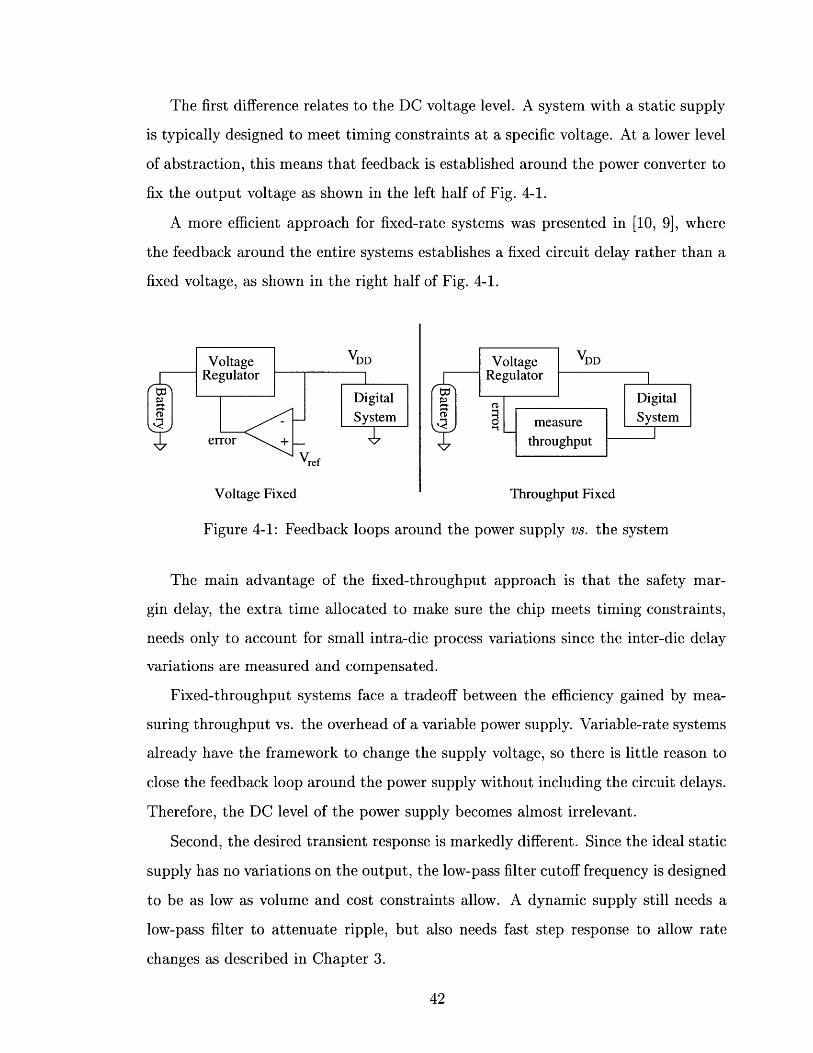
The first difference relates to the DC voltage level. A system with a static supply
is typically designed to meet timing constraints at a specific voltage. At a lower level
of abstraction, this means that feedback is established around the power converter to
fix the output voltage as shown in the left half of Fig. 4-1.
A more efficient approach for fixed-rate systems was presented in [10, 9], where
the feedback around the entire systems establishes a fixed circuit delay rather than a
fixed voltage, as shown in the right half of Fig. 4-1.
Vref
v xLeg•d iI cU1 A1IUUP1UL XFtAU
Figure 4-1: Feedback loops around the power supply vs. the system
The main advantage of the fixed-throughput approach is that the safety mar-
gin delay, the extra time allocated to make sure the chip meets timing constraints,
needs only to account for small intra-die process variations since the inter-die delay
variations are measured and compensated.
Fixed-throughput systems face a tradeoff between the efficiency gained by mea-
suring throughput vs. the overhead of a variable power supply. Variable-rate systems
already have the framework to change the supply voltage, so there is little reason to
close the feedback loop around the power supply without including the circuit delays.
Therefore, the DC level of the power supply becomes almost irrelevant.
Second, the desired transient response is markedly different. Since the ideal static
supply has no variations on the output, the low-pass filter cutoff frequency is designed
to be as low as volume and cost constraints allow. A dynamic supply still needs a
low-pass filter to attenuate ripple, but also needs fast step response to allow rate
changes as described in Chapter 3.
Th
h Fi
d
4.2 Supply topology
4.2.1 Linear regulator
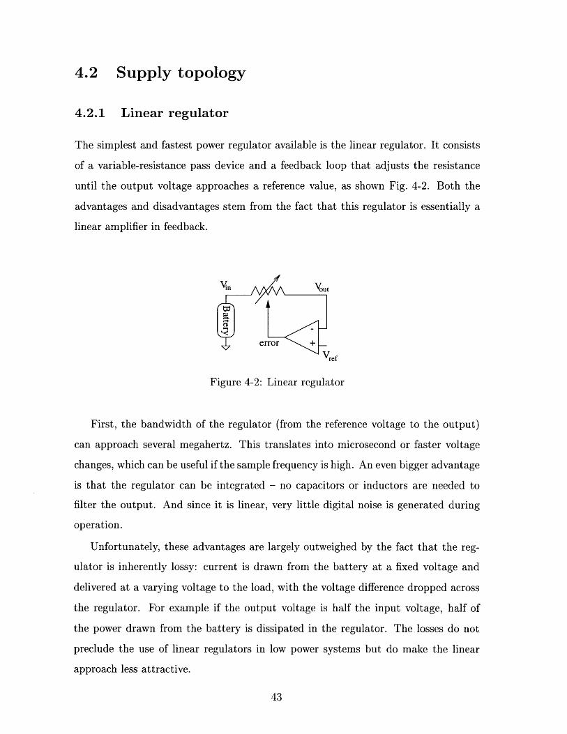
The simplest and fastest power regulator available is the linear regulator. It consists
of a variable-resistance pass device and a feedback loop that adjusts the resistance
until the output voltage approaches a reference value, as shown Fig. 4-2. Both the
advantages and disadvantages stem from the fact that this regulator is essentially a
linear amplifier in feedback.
Vref
Figure 4-2: Linear regulator
First, the bandwidth of the regulator (from the reference voltage to the output)
can approach several megahertz. This translates into microsecond or faster voltage
changes, which can be useful if the sample frequency is high. An even bigger advantage
is that the regulator can be integrated - no capacitors or inductors are needed to
filter the output. And since it is linear, very little digital noise is generated during
operation.
Unfortunately, these advantages are largely outweighed by the fact that the reg-
ulator is inherently lossy: current is drawn from the battery at a fixed voltage and
delivered at a varying voltage to the load, with the voltage difference dropped across
the regulator. For example if the output voltage is half the input voltage, half of
the power drawn from the battery is dissipated in the regulator. The losses do not
preclude the use of linear regulators in low power systems but do make the linear
approach less attractive.

4.2.2 Switched capacitor converter
Switched capacitor charge pumps can also be used as power converters [5]. Power is
transferred in a step-up (step-down) converter by charging two capacitors in parallel
(series) and discharging them in series (parallel). The schematic (Fig. 4-3) is the
same, and power flow is determined by placement of the source and load. Other
configurations are possible to give any rational conversion ratio, though the ratio is
fixed by the topology.
VC-- T C2 V2
C1Cs
Figure 4-3: Switched-capacitor converter
For step-up operation, a voltage source (i.e. a battery) is placed on the low-V
side and the load, typically modeled as a resistor or current source, on the high-V
side. The capacitor C, is charged to V1 during q 1, and then switched in series with
C1 during 02 to give double the voltage. A charge 6Q flows into C2, voltage across C,
drops by 6V = 6Q/C, and then the capacitor is switched back and the cycle repeats.
Step-down operation is the same, except charge flows in the other direction.
Energy is lost in this converter when capacitors with different voltages are con-
nected together: on 01 Cs is charged from V1 - 6V to V1 and during 02 it discharges
back to V1 - 6V. This can be modeled as an effective resistance in series with the
output of value equal to Reff = 1/f5 Cs where f, is the switching frequency.
In principle, all of the components in the converter could be integrated. However,
regulation is tricky (a different set of capacitors would be needed for each fraction of
the input voltage), and to keep Reff low off-chip capacitors are usually required.

4.2.3 Switching converter
Unlike a linear regulator, the switching converter is a sampled rather than a con-
tinuous time system. A representative switching converter called a buck converter is
shown in Fig. 4.2.3.
Vbattery
Vgp9-0
Vgn
out
Rload
Figure 4-4: Simplified buck converter schematic
When transistor M1 is on and M2 off, voltage V, rises to VDD. Conversely, with
M2 on and M1 off, V, approaches ground. The duty cycle of the resultant square wave
on V, determines the DC level of the output voltage and the ripple is attenuated by
an LC filter.
Unlike the linear regulator where losses were inherent in the operation, the power
loss in the buck converter is due to parasitics - the losses approach 0 with ideal
elements, and efficiencies of over 90% have been reported [16]. The major losses are
due to series resistance in the inductor and switches, and the CV2f power due to the
gate and junction capacitance of the switches.
Both the series resistance and the gate capacitance of the switches depends on the
channel length of the switching FET in the same way, so the L of the devices should
be minimized. However, the resistance goes down with width and the capacitance
increases, so there is a trade-off for W. A convenient result from the optimization is
that at the minimum power point, equal power is dissipated in the series resistance
of the switches and in driving the gate.
Active Damping
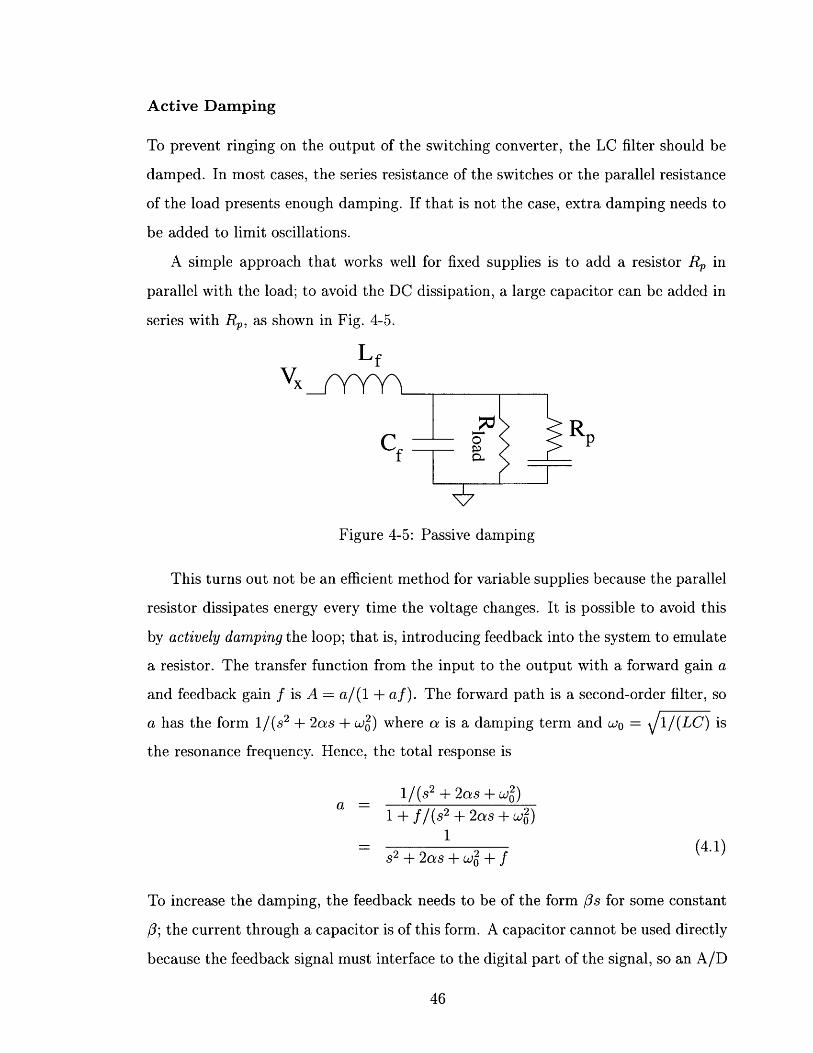
To prevent ringing on the output of the switching converter, the LC filter should be
damped. In most cases, the series resistance of the switches or the parallel resistance
of the load presents enough damping. If that is not the case, extra damping needs to
be added to limit oscillations.
A simple approach that works well for fixed supplies is to add a resistor Rp in
parallel with the load; to avoid the DC dissipation, a large capacitor can be added in
series with Rp, as shown in Fig. 4-5.
Lf
C f
Figure 4-5: Passive damping
This turns out not be an efficient method for variable supplies because the parallel
resistor dissipates energy every time the voltage changes. It is possible to avoid this
by actively damping the loop; that is, introducing feedback into the system to emulate
a resistor. The transfer function from the input to the output with a forward gain a
and feedback gain f is A = a/(1 + af). The forward path is a second-order filter, so
a has the form 1/(s 2 + 2as + W2o) where a is a damping term and wo = 1/(LC) is
the resonance frequency. Hence, the total response is
1/(s2 + 2as + w2)1a + f/(s2 + 2as + 2)
1=2 +f (4.1)2 + 2as + w f (4.1)
To increase the damping, the feedback needs to be of the form ps for some constant
/; the current through a capacitor is of this form. A capacitor cannot be used directly
because the feedback signal must interface to the digital part of the signal, so an A/D
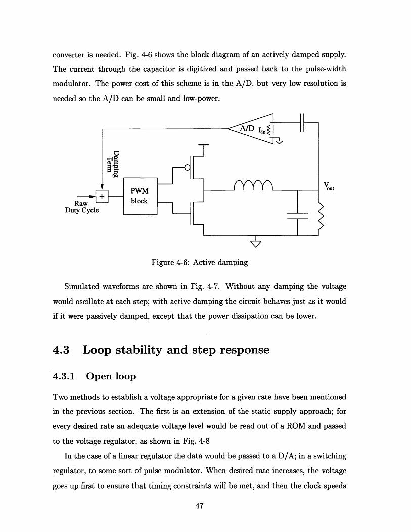
converter is needed. Fig. 4-6 shows the block diagram of an actively damped supply.
The current through the capacitor is digitized and passed back to the pulse-width
modulator. The power cost of this scheme is in the A/D, but very low resolution is
needed so the A/D can be small and low-power.
Vout
Dut'
Figure 4-6: Active damping
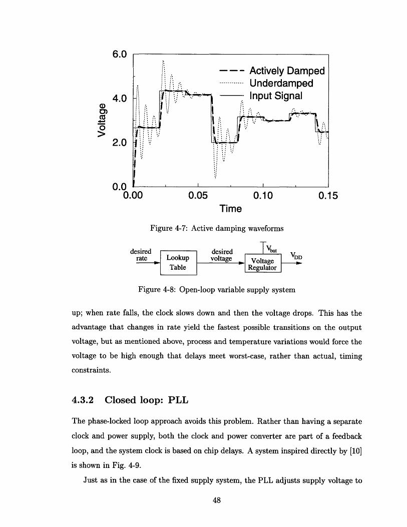
Simulated waveforms are shown in Fig. 4-7. Without any damping the voltage
would oscillate at each step; with active damping the circuit behaves just as it would
if it were passively damped, except that the power dissipation can be lower.
4.3 Loop stability and step response
4.3.1 Open loop
Two methods to establish a voltage appropriate for a given rate have been mentioned
in the previous section. The first is an extension of the static supply approach; for
every desired rate an adequate voltage level would be read out of a ROM and passed
to the voltage regulator, as shown in Fig. 4-8
In the case of a linear regulator the data would be passed to a D/A; in a switching
regulator, to some sort of pulse modulator. When desired rate increases, the voltage
goes up first to ensure that timing constraints will be met, and then the clock speeds
I:,,'U.U
4.0CU
0o
2.0
nnA
0.00 0.05 0.10 0.15Time
Figure 4-7: Active damping waveforms
Figure 4-8: Open-loop variable supply system
up; when rate falls, the clock slows down and then the voltage drops. This has the
advantage that changes in rate yield the fastest possible transitions on the output
voltage, but as mentioned above, process and temperature variations would force the
voltage to be high enough that delays meet worst-case, rather than actual, timing
constraints.
4.3.2 Closed loop: PLL
The phase-locked loop approach avoids this problem. Rather than having a separate
clock and power supply, both the clock and power converter are part of a feedback
loop, and the system clock is based on chip delays. A system inspired directly by [10]
is shown in Fig. 4-9.
Just as in the case of the fixed supply system, the PLL adjusts supply voltage to
--- Actively DampedUnderdamped
i Input Signal
I ,,
.:,
.
I:, ' ' :
rate
Ref. clocl
Figure 4-9: Block diagram of a phase-locked loop
the lowest possible level compatible with the required number of gate delays between
registers. When the desired rate changes, the reference clock that the PLL sees
changes and the loop re-locks. The drawback is in the time constant of the changes.
The time constant is determined by the bandwidth of the power supply, the loop
filter, and the extra pole introduced by the integration of frequency to phase. With
no loop filter, the feedback pole at 0 combines with the second-order pole1 from the
power supply to give a peaked response loop gain. A loop filter with a bandwidth
significantly less than that of the power supply output filters can be added, but then
this bandwidth limits how fast the loop locks.
4.3.3 Hybrid approach
The two previous schemes, the PLL and the lookup table, adjust the output voltage at
different rates because they were originally intended for different functions. The PLL
does best in tracking process variations where its low bandwidth is sufficient, and the
lookup table is well suited to making fast voltage steps to predefined level. In fact,
the characteristics are not mutually exclusive; it is possible to merge the lookup-table
approach with the phase-locked loop to get fast voltage steps and process tracking at
the same time.
The lookup table should still be used to get the fastest possible voltage changes;
however, if the voltage levels are stored in a RAM instead of ROM they can updated
to track process and temperature. A schematic is shown in Fig. 4-10.
1Assuming a switching supply with an LC output filter.
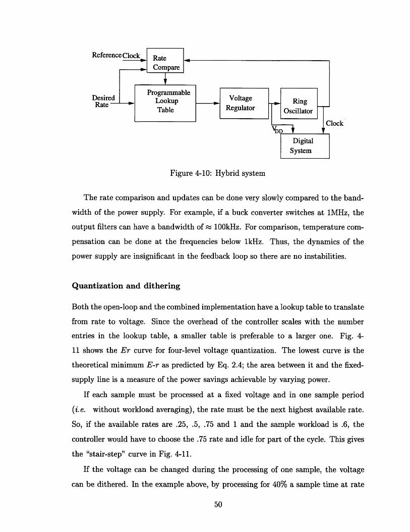
Figure 4-10: Hybrid system
The rate comparison and updates can be done very slowly compared to the band-
width of the power supply. For example, if a buck converter switches at 1MHz, the
output filters can have a bandwidth of r 100kHz. For comparison, temperature com-
pensation can be done at the frequencies below 1kHz. Thus, the dynamics of the
power supply are insignificant in the feedback loop so there are no instabilities.
Quantization and dithering
Both the open-loop and the combined implementation have a lookup table to translate
from rate to voltage. Since the overhead of the controller scales with the number
entries in the lookup table, a smaller table is preferable to a larger one. Fig. 4-
11 shows the Er curve for four-level voltage quantization. The lowest curve is the
theoretical minimum E-r as predicted by Eq. 2.4; the area between it and the fixed-
supply line is a measure of the power savings achievable by varying power.
If each sample must be processed at a fixed voltage and in one sample period
(i.e. without workload averaging), the rate must be the next highest available rate.
So, if the available rates are .25, .5, .75 and 1 and the sample workload is .6, the
controller would have to choose the .75 rate and idle for part of the cycle. This gives
the "stair-step" curve in Fig. 4-11.
If the voltage can be changed during the processing of one sample, the voltage
can be dithered. In the example above, by processing for 40% a sample time at rate
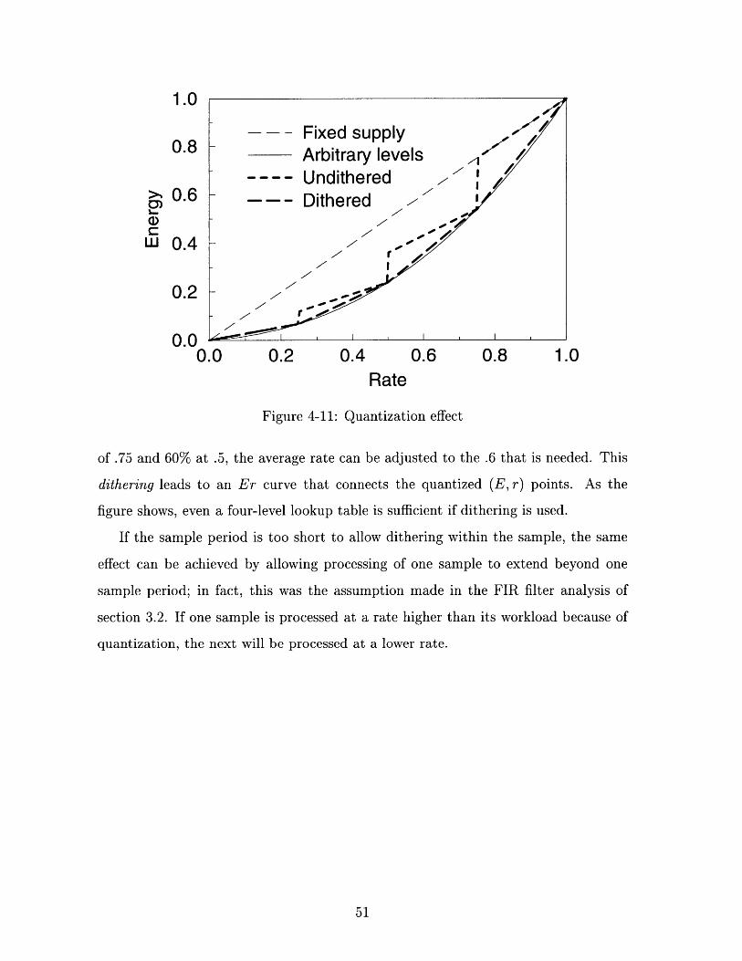
.1 F~
I.UV
0.8
S0.6
C:Lu 0.4
0.2
A Av.v
0.0 0.2 0.4 0.6 0.8 1.0Rate
Figure 4-11: Quantization effect
of .75 and 60% at .5, the average rate can be adjusted to the .6 that is needed. This
dithering leads to an Er curve that connects the quantized (E, r) points. As the
figure shows, even a four-level lookup table is sufficient if dithering is used.
If the sample period is too short to allow dithering within the sample, the same
effect can be achieved by allowing processing of one sample to extend beyond one
sample period; in fact, this was the assumption made in the FIR filter analysis of
section 3.2. If one sample is processed at a rate higher than its workload because of
quantization, the next will be processed at a lower rate.
- -- -Fixed supplyArbitrary levels /1
- - - - Undithered /Dithered
r
7
I

Chapter 5
Implementation and Testing
5.1 Chip design
A chip was designed to test the stability of the feedback loop and to verify that
timing constraints are met as the modified phase-locked loop changes the clock and
supply voltage. Since the focus is on the variable supply voltage control, only a
token amount of processing is done by the DSP section, but it can be reconfigured to
emulate applications with long sample periods (i.e., computationally intensive cases
like video processing) as well as applications with shorter sample periods. Similarly,
the rest of the circuitry is designed for flexibility rather than efficiency.
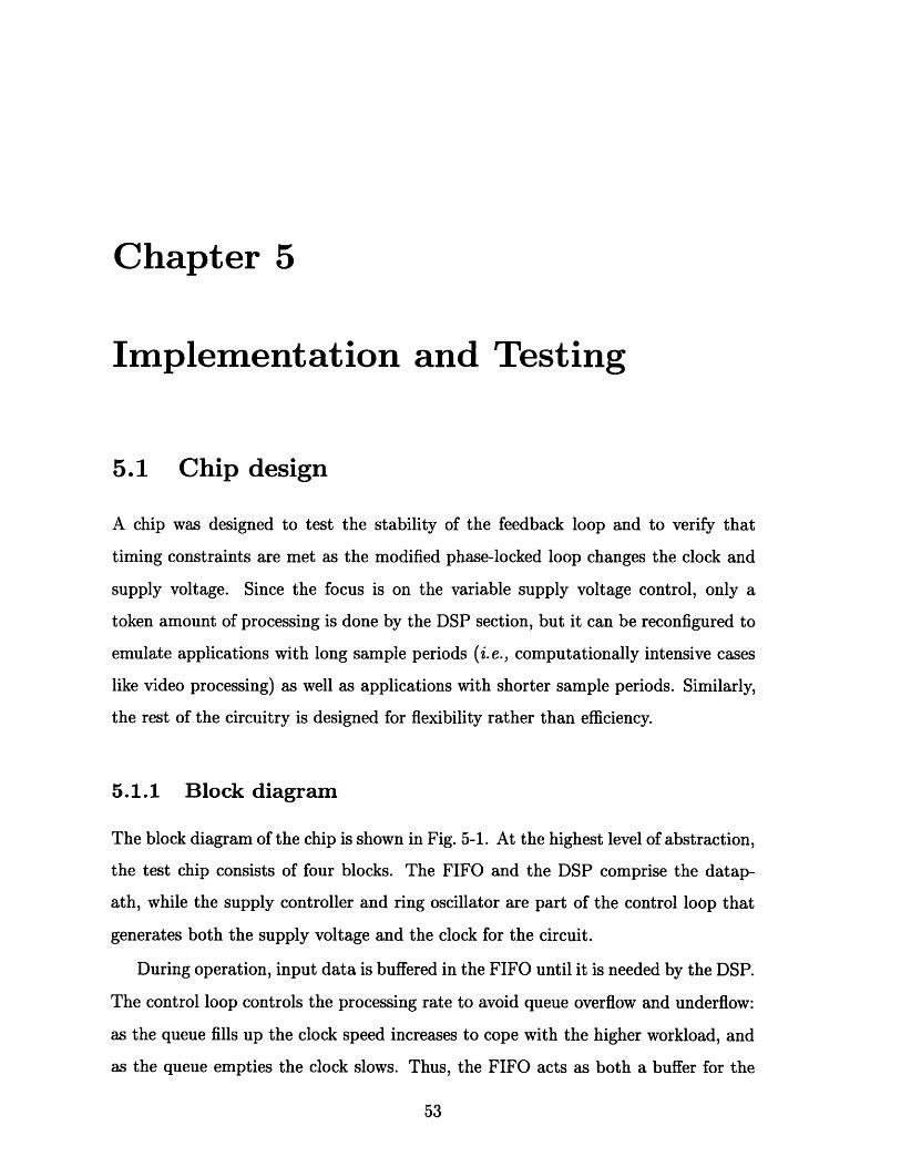
5.1.1 Block diagram
The block diagram of the chip is shown in Fig. 5-1. At the highest level of abstraction,
the test chip consists of four blocks. The FIFO and the DSP comprise the datap-
ath, while the supply controller and ring oscillator are part of the control loop that
generates both the supply voltage and the clock for the circuit.
During operation, input data is buffered in the FIFO until it is needed by the DSP.
The control loop controls the processing rate to avoid queue overflow and underflow:
as the queue fills up the clock speed increases to cope with the higher workload, and
as the queue empties the clock slows. Thus, the FIFO acts as both a buffer for the
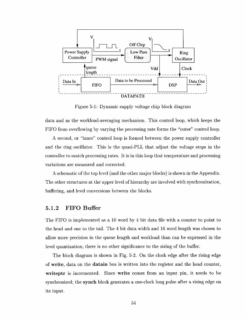
-queue Vdd_ |Clocklength
Data In Data to be Processed Data OutS FIFO DSP
DATAPATH
Figure 5-1: Dynamic supply voltage chip block diagram
data and as the workload-averaging mechanism. This control loop, which keeps the
FIFO from overflowing by varying the processing rate forms the "outer" control loop.
A second, or "inner" control loop is formed between the power supply controller
and the ring oscillator. This is the quasi-PLL that adjust the voltage steps in the
controller to match processing rates. It is in this loop that temperature and processing
variations are measured and corrected.
A schematic of the top level (and the other major blocks) is shown in the Appendix.
The other structures at the upper level of hierarchy are involved with synchronization,
buffering, and level conversions between the blocks.
5.1.2 FIFO Buffer
The FIFO is implemented as a 16 word by 4 bit data file with a counter to point to
the head and one to the tail. The 4 bit data width and 16 word length was chosen to
allow more precision in the queue length and workload than can be expressed in the
level quantization; there is no other significance to the sizing of the buffer.
The block diagram is shown in Fig. 5-2. On the clock edge after the rising edge
of write, data on the datain bus is written into the register and the head counter,
writeptr is incremented. Since write comes from an input pin, it needs to be
synchronized; the synch block generates a one-clock long pulse after a rising edge on
its input.
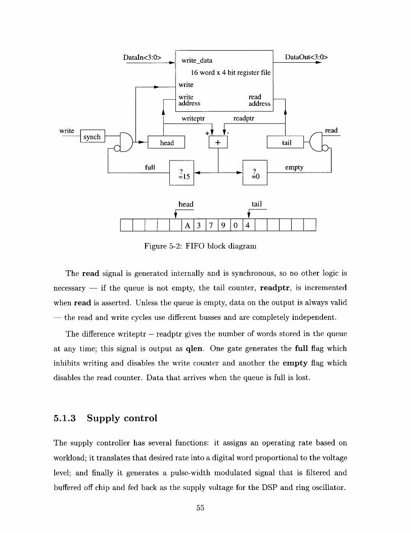
write data
16 word x 4 bit register file
write
write readaddress address
read
head tail
I I A 3 1 9 0 14 1
Figure 5-2: FIFO block diagram
The read signal is generated internally and is synchronous, so no other logic is
necessary - if the queue is not empty, the tail counter, readptr, is incremented
when read is asserted. Unless the queue is empty, data on the output is always valid
- the read and write cycles use different busses and are completely independent.
The difference writeptr - readptr gives the number of words stored in the queue
at any time; this signal is output as qlen. One gate generates the full flag which
inhibits writing and disables the write counter and another the empty flag which
disables the read counter. Data that arrives when the queue is full is lost.
5.1.3 Supply control
The supply controller has several functions: it assigns an operating rate based on
workload; it translates that desired rate into a digital word proportional to the voltage
level; and finally it generates a pulse-width modulated signal that is filtered and
buffered off chip and fed back as the supply voltage for the DSP and ring oscillator.
Dataln<3:0> DataOut<3:0>
N
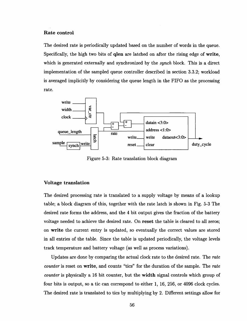
Rate control
The desired rate is periodically updated based on the number of words in the queue.
Specifically, the high two bits of qlen are latched on after the rising edge of write,
which is generated externally and synchronized by the synch block. This is a direct
implementation of the sampled queue controller described in section 3.3.2; workload
is averaged implicitly by considering the queue length in the FIFO as the processing
rate.
cycle
Figure 5-3: Rate translation block diagram
Voltage translation
The desired processing rate is translated to a supply voltage by means of a lookup
table; a block diagram of this, together with the rate latch is shown in Fig. 5-3 The
desired rate forms the address, and the 4 bit output gives the fraction of the battery
voltage needed to achieve the desired rate. On reset the table is cleared to all zeros;
on write the current entry is updated, so eventually the correct values are stored
in all entries of the table. Since the table is updated periodically, the voltage levels
track temperature and battery voltage (as well as process variations).
Updates are done by comparing the actual clock rate to the desired rate. The rate
counter is reset on write, and counts "tics" for the duration of the sample. The rate
counter is physically a 16 bit counter, but the width signal controls which group of
four bits is output, so a tic can correspond to either 1, 16, 256, or 4096 clock cycles.
The desired rate is translated to tics by multiplying by 2. Different settings allow for
faster or slower updates.
The count at the end of the sample period (i.e. at write) is subtracted from the
desired rate to get the rate error. The error is then added the the current lookup
table entry before the address changes. So, if the rate was too high (low), the error
is negative (positive) and the voltage entry is lowered (raised). In the event of over
or underflow, the value entered is limited to all ones or all zeros, respectively.
For example, the entry for rate = 3 in the lookup table might be 14. If the actual
tic-count at the end of the sample period were 7, the error - 2 x rate - 7 = -1 -
would be added to the lookup table entry, and the new value would be 13. If, on the
other hand, the tic-count at write were 4, the error would be 6 - 4 = 2 and the new
entry should be 16; since that overflows the 4-bit words of the lookup table the actual
entry is limited to 15.
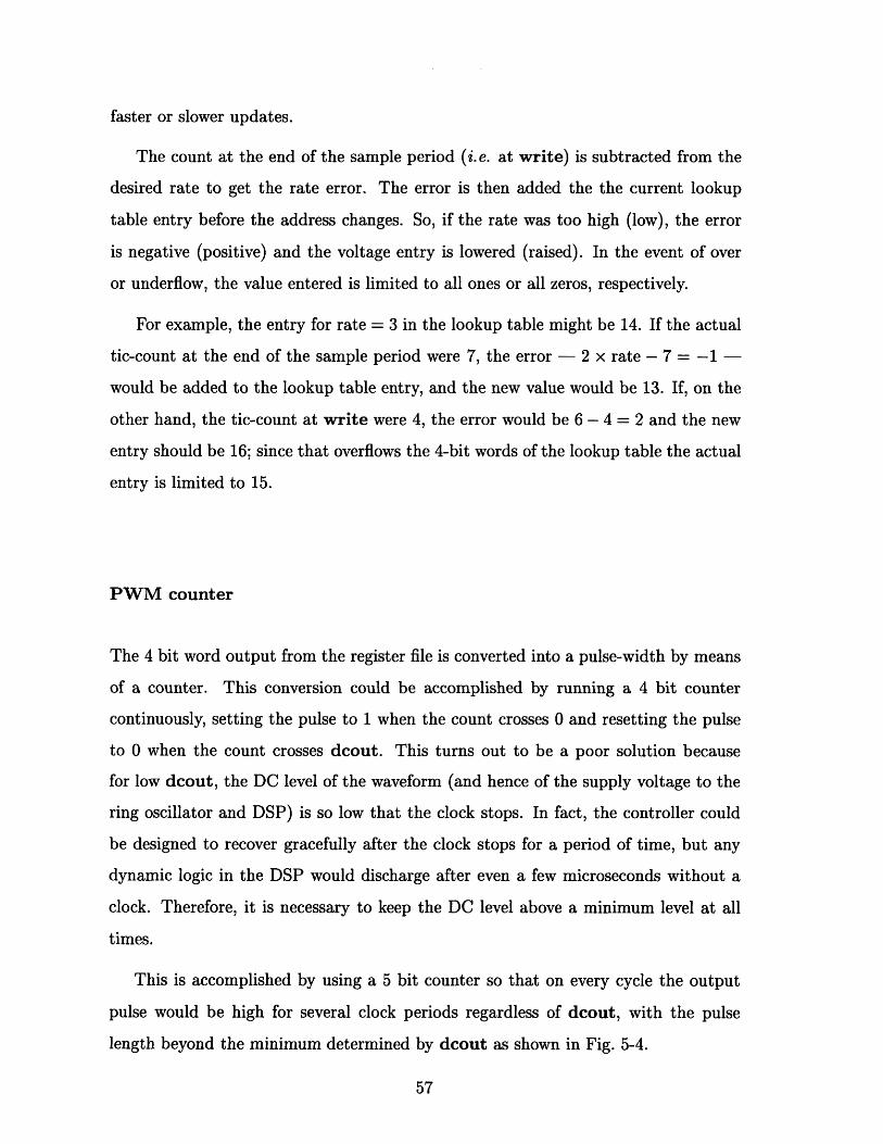
PWM counter
The 4 bit word output from the register file is converted into a pulse-width by means
of a counter. This conversion could be accomplished by running a 4 bit counter
continuously, setting the pulse to 1 when the count crosses 0 and resetting the pulse
to 0 when the count crosses dcout. This turns out to be a poor solution because
for low dcout, the DC level of the waveform (and hence of the supply voltage to the
ring oscillator and DSP) is so low that the clock stops. In fact, the controller could
be designed to recover gracefully after the clock stops for a period of time, but any
dynamic logic in the DSP would discharge after even a few microseconds without a
clock. Therefore, it is necessary to keep the DC level above a minimum level at all
times.
This is accomplished by using a 5 bit counter so that on every cycle the output
pulse would be high for several clock periods regardless of dcout, with the pulse
length beyond the minimum determined by dcout as shown in Fig. 5-4.
PWM
I I I I
minimum duty cycle
Figure 5-4: PWM block diagram
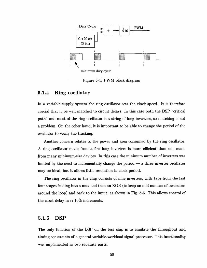
5.1.4 Ring oscillator
In a variable supply system the ring oscillator sets the clock speed. It is therefore
crucial that it be well matched to circuit delays. In this case both the DSP "critical
path" and most of the ring oscillator is a string of long inverters, so matching is not
a problem. On the other hand, it is important to be able to change the period of the
oscillator to verify the tracking.
Another concern relates to the power and area consumed by the ring oscillator.
A ring oscillator made from a few long inverters is more efficient than one made
from many minimum-size devices. In this case the minimum number of inverters was
limited by the need to incrementally change the period - a three inverter oscillator
may be ideal, but it allows little resolution in clock period.
The ring oscillator in the chip consists of nine inverters, with taps from the last
four stages feeding into a mux and then an XOR (to keep an odd number of inversions
around the loop) and back to the input, as shown in Fig. 5-5. This allows control of
the clock delay in - 10% increments.
5.1.5 DSP
The only function of the DSP on the test chip is to emulate the throughput and
timing constraints of a general variable-workload signal processor. This functionality
was implemented as two separate parts.
1

1 n-3 n-2 n-1 n
Figure 5-5: Ring oscillator block diagram
Any algorithm that terminates on a data-dependent condition generates a variable
workload. For example, an algebraic approximation iteration that terminates when
the desired precision is reached, or a video decompression procedure that processes
data until it finds an end-of-frame marker both appear as variable workload algo-
rithms. One of the simplest algorithms is a counter: it counts from zero until the
count matches the input data. When the count matches, the data word is considered
"processed," and another word is fetched from the FIFO. To verify that the right
words are being fetched and executed, the counter state is an output of the chip.
Ideally, the variable supply chip could emulate both the computationally long
samples common in video processing and the very short samples typical in commu-
nications systems. The four bit input words allow sixteen levels of workload for the
DSP. The sixteen levels are sufficient to exercise the DSP at a fixed sample com-
plexity, but are completely inadequate to span the orders of magnitude complexity
needed. Rather than increasing the length of the data word (and with it, the buffer
size) the complexity per sample is controlled by selecting one of four sets of four bits
from the sixteen bit counter get treated as the "processing." The block diagram of
the DSP is shown in Fig. 5-6.
The critical path consists of strings of long inverters placed between the counter
and output latches. Since timing errors can only occur when the input is changing,
the input to these delay chains comes from the lowest four bits of the sixteen bit DSP
counter, independent of which bits actually form the "output" of the chip. Thus,
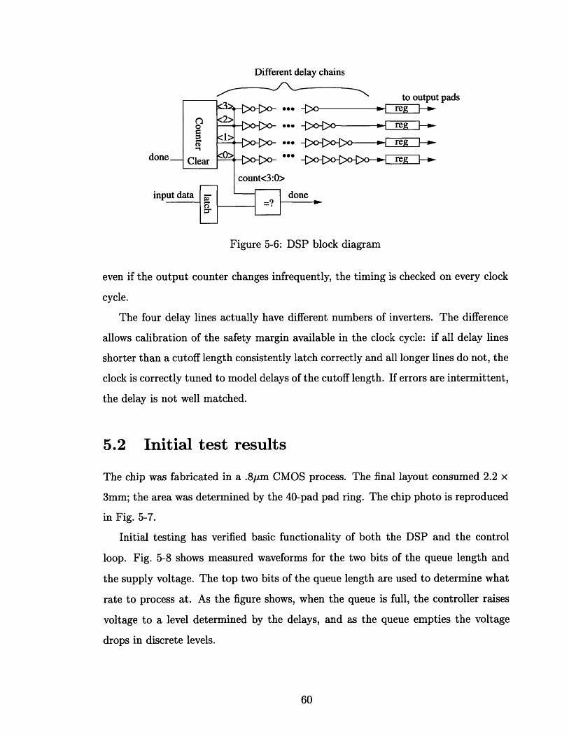
Different delay chains
tn nitnllt nfrl
I reg -
'-. reg
Figure 5-6: DSP block diagram
even if the output counter changes infrequently, the timing is checked on every clock
cycle.
The four delay lines actually have different numbers of inverters. The difference
allows calibration of the safety margin available in the clock cycle: if all delay lines
shorter than a cutoff length consistently latch correctly and all longer lines do not, the
clock is correctly tuned to model delays of the cutoff length. If errors are intermittent,
the delay is not well matched.
5.2 Initial test results
The chip was fabricated in a .8pm CMOS process. The final layout consumed 2.2 x
3mm; the area was determined by the 40-pad pad ring. The chip photo is reproduced
in Fig. 5-7.
Initial testing has verified basic functionality of both the DSP and the control
loop. Fig. 5-8 shows measured waveforms for the two bits of the queue length and
the supply voltage. The top two bits of the queue length are used to determine what
rate to process at. As the figure shows, when the queue is full, the controller raises
voltage to a level determined by the delays, and as the queue empties the voltage
drops in discrete levels.
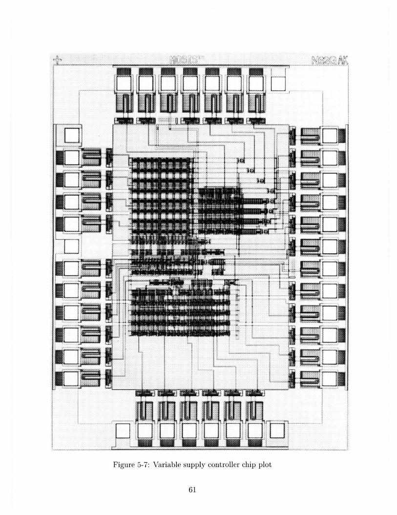
l%~.t~$~; :-*~x·i;ii
I
I
i
~zieti
-t
Figure 5-7: Variable supply controller chip plot
,7 7...... .
ri
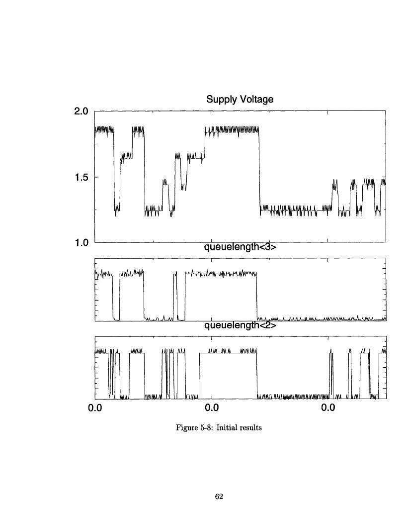
Supply Voltage
queuelength<2>
J I
0.0 0.0
Figure 5-8: Initial results
2.0
1.5
1.0
0.0
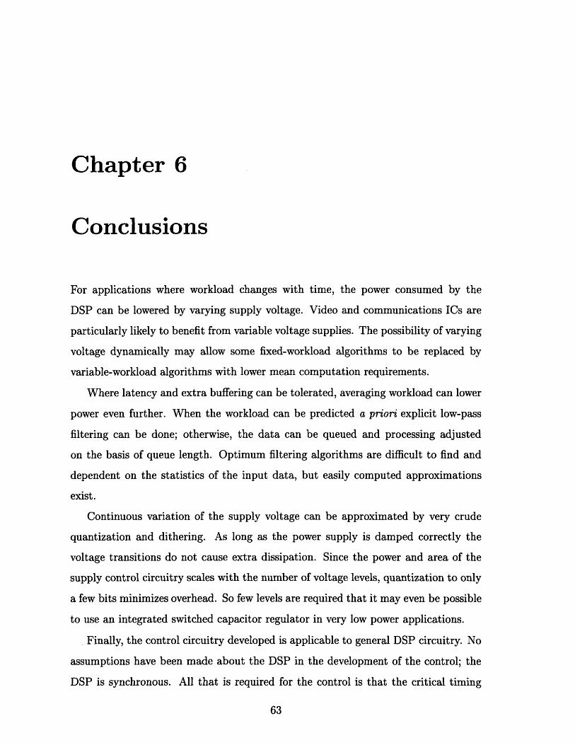
Chapter 6
Conclusions
For applications where workload changes with time, the power consumed by the
DSP can be lowered by varying supply voltage. Video and communications ICs are
particularly likely to benefit from variable voltage supplies. The possibility of varying
voltage dynamically may allow some fixed-workload algorithms to be replaced by
variable-workload algorithms with lower mean computation requirements.
Where latency and extra buffering can be tolerated, averaging workload can lower
power even further. When the workload can be predicted a priori explicit low-pass
filtering can be done; otherwise, the data can be queued and processing adjusted
on the basis of queue length. Optimum filtering algorithms are difficult to find and
dependent on the statistics of the input data, but easily computed approximations
exist.
Continuous variation of the supply voltage can be approximated by very crude
quantization and dithering. As long as the power supply is damped correctly the
voltage transitions do not cause extra dissipation. Since the power and area of the
supply control circuitry scales with the number of voltage levels, quantization to only
a few bits minimizes overhead. So few levels are required that it may even be possible
to use an integrated switched capacitor regulator in very low power applications.
Finally, the control circuitry developed is applicable to general DSP circuitry. No
assumptions have been made about the DSP in the development of the control; the
DSP is synchronous. All that is required for the control is that the critical timing
-0
)ut
Figure 6-1: Parasitic losses in buck converter
path is known.
6.1 Variable supply tradeoffs
The only advantage of variable supply systems is the lower power. The tradeoffs
required in the power supply to achieve this power savings are included in the calcu-
lation. However, there are several secondary drawbacks that a variable supply system
necessarily suffers. This section discusses some of the drawbacks specific to variable
supply systems.
A few circuit optimization techniques depend on a fixed supply voltage. For
example, it is possible to equalize rise and fall times in static gates by sizing the
devices properly; the exact sizes depend on the supply voltage. More significant
effects are felt by the power converter.
Power supplies
One of the losses associated with switching power supplies is due to the CV2 f loss in
the parasitic capacitance on the high-frequency output node; in Fig. 6-1 this is the
capacitor CQ.
In the case of large switching devices, Cx is dominated by the drain capacitance of
the switching devices. A technique to eliminate this loss called "soft switching" relies
on adjusting the drive waveforms to avoid discharging CQ through the drive devices
[16]. By adjusting the delay between turning off one of the switches and turning on
the other one, it is possible to turn on the FETs only when they have nearly OV VDS,
thus eliminating switching losses.
Unfortunately, the exact timing depends on the current flowing in the inductor.
If the output voltage is constant, the feedback loop suggested in [16] can adjust the
timing. In a variable supply system the current changes with every voltage change,
so there would be an unavoidable loss with every transition while the loop re-locks.
If voltage changes frequently, soft switching becomes untenable.
6.2 Future research
This thesis describes the framework for implementing a variable power supply system.
Specifics of the implementation would need to be investigated for each particular
system; the approximations needed by a 10W system are completely different from
those needed by a 10mW system. However, there are several issues specific to variable
supply systems in general that need to be developed further.
6.2.1 Testability
Testing of a variable voltage system is somewhat more involved than that of a fixed
supply system: not only does the functionality have to be verified for all the internal
states of the system, but also for a range of voltages. So, a DSP chip that works at 3V
may not work correctly at 2V if the clock generation was misdesigned or misfabricated.
6.2.2 Interaction of multiple systems
The thesis has assumed that a variable voltage IC would be embedded in a fixed-clock
system. It may be the case that for large enough systems, it will be useful to put
several different variable voltage chips together into a larger block. Another possibility
is that several subsystems with separate variable supplies would be integrated onto a
single chip. In either case, the interactions of the chips should be explored.
Specifically, the data rate at the output of a variable clock system is not the same
as the input data rate. For proper operation, a macro-controller may need to be
developed to manage power consumption of the whole system.
Bibliography
[1] Vincent R. von Kaenel et. al. . Automatic adjustment of threshold and supply
voltages for minimum power consumption in CMOS digital circuits. In IEEE
Symposium on Low Power Electronics, pages 78-79, 1994.
[2] Lars S. Nielsen et. al. . Low-power operation using self-timed circuits and adap-
tive scaling of the supply voltage. IEEE Transactions on VLSI, 2(4):391-397,
December 1994.
[3] L. G. Heller and W.R. Griffin. Cascode voltage switch logic: A differential CMOS
logic family. ISSCC Digest of Technical Papers, pages 16-17, February 1984.
[4] Gordon M. Jacobs and Robert W. Brodersen. A fully asynchronous digital signal
processor using self-timed circuits. Journal of Solid State-State Circuits, pages
1526-1537, December 1990.
[5] Anantha Chandrakasan and Robert Brodersen. Low Power Digital CMOS De-
sign. Kluwer Academic Publishers, 1995.
[6] R. M. Swanson and J.D. Meindl. Ion-implanted complementary MOS transistors
in low-voltage circuits. IEEE Journal of Solid-State Circuits, 7(2):146-152, April
1972.
[7] M. Mutoh et. al. . 1-V power supply high-speed digital circuit technology with
multithreshold voltage CMOS. IEEE Journal of Solid State Circuits, pages 847-
854, August 1995.
[8] K. Seta et. al. 50% active-power saving without speed degradation using standby
power reduction (SPR) circuit. In IEEE International Solid-State Circuits Con-
ference, pages 318-319, 1995.
[9] Marc Horowitz. Low power processor design using self clocking. ARPA Low
Power Electronics Annual Review, April 1995.
[10] Peter Macken et. al. . A voltage reduction technique for digital systems. In
Digest of Technical Papers, IEEE International Solid-State Circuits Conference,
pages 238-239, February 1990.
[11] J. Ludwig, H. Nawab, and A. Chandrakasan. Low power digital filtering using
approximate processing. IEEE Journal of Solid-State Circuits, March 1996.
[12] A.P. Chandrakasan, S. Sheng, and R.W. Brodersen. Low-power CMOS digital
design. IEEE J. Solid-State Circuits, 27(4):473-483, April 1992.
[13] C. Sodini, P. K. Ko, and J. L. Moll. The effect of high fields on MOS devices
and circuit performance. IEEE Transactions on Electron Devices, 31:1386-1393,
Oct 1984.
[14] M. Kakumu and M. Kinagawa. Power-supply voltage impact on circuit perfor-
mance for half and lower submicrometer CMOS LSI. IEEE Transactions on
Electron Devices, 37(8):1902-1908, August 1990.
[15] Thomas M. Cover and Joy A. Thomas. Elements of Information Theory. Wiley
Series in Telecommunications. John Wiley & Sons, 1991.
[16] A. Stratakos, S. Sanders, and R. Brodersen. A low-voltage CMOS DC-DC con-
verter for a portable low-powered battery-operated system. PESC, 1994.
Appendix A
Schematics

x x
X X
x x
Figure A-1: Top level schematics
I )
x
x
,Q
ro.
Uo~0 l0 a ,·,
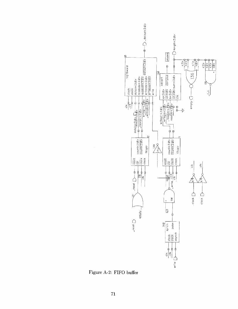
A
V
-a
Figure A-2: FIFO buffer
o o
0 0U U
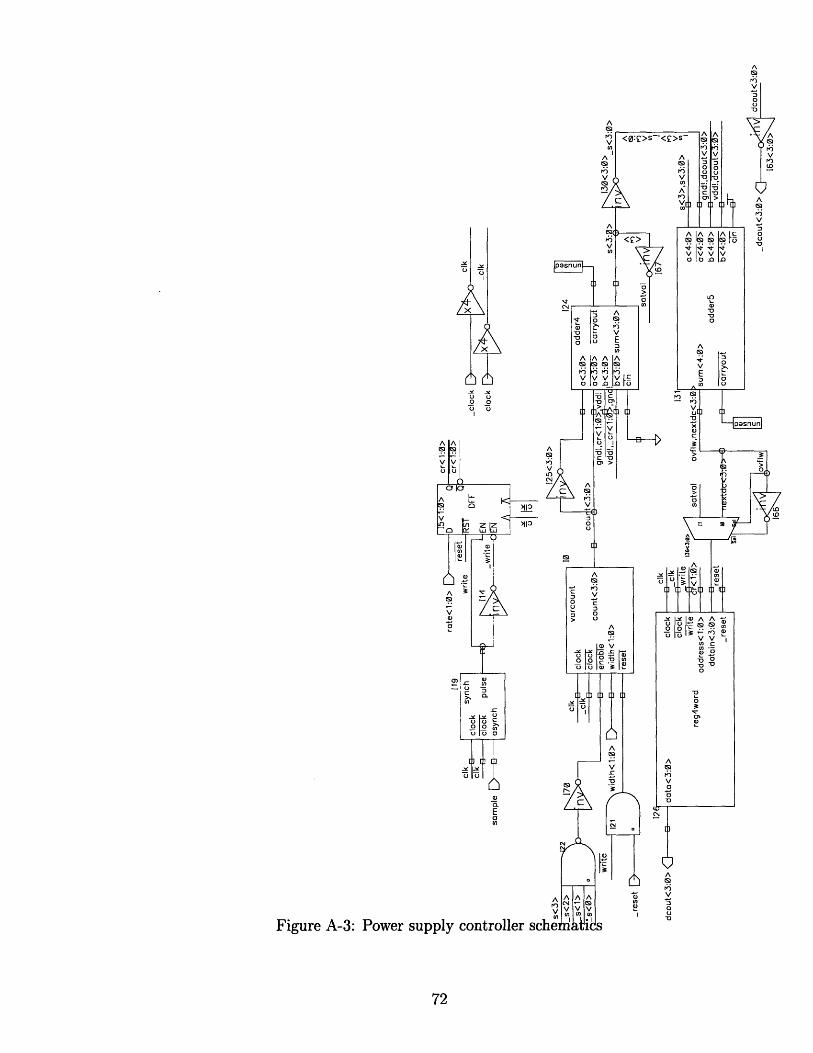
x
x6U-r xo oo 0o 0
Figure A-3: Power supply controller
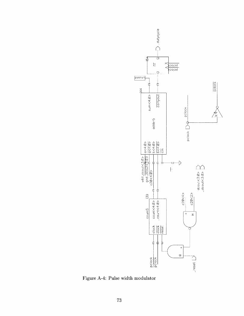
AA
M),
v v
o 1OO
Figure A-4: Pulse width modulator
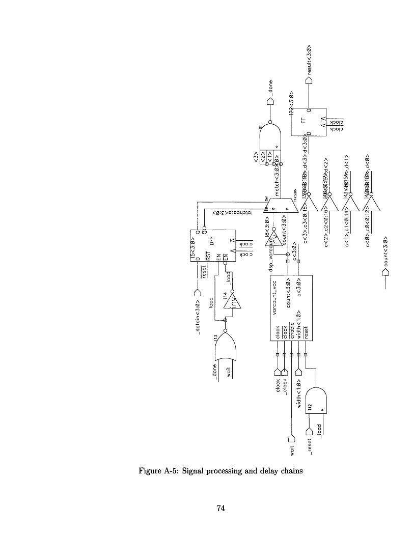
A A
V V
VVv _
A A
V V Vo o
Figure A-5: Signal processing and delay chains
74
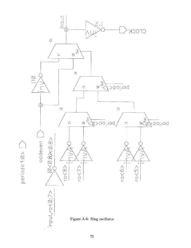
~)1313M
cQ)slý
,>(j d- ® v~i¾: >~ooid
>poied
A
V0,
Figure A-6: Ring oscillatorC
A00CD
V00
n)
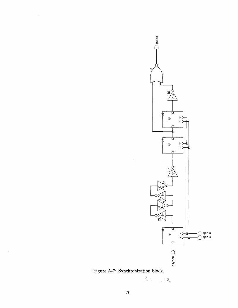
0)(nCL
Figure A-7: Synchronization block