a fresh look at dram architecture: new techniques to
TRANSCRIPT

A Fresh Look at DRAM Architecture: New Techniques to Improve DRAM
Latency, Parallelism, and Energy Efficiency
Onur Mutlu [email protected]
July 4, 2013 INRIA
Video Lectures on Same Topics n Videos from a similar series of lectures at Bogazici
University (these are longer)
n http://www.youtube.com/playlist?list=PLVngZ7BemHHV6N0ejHhwOfLwTr8Q-UKXj
n DRAM Basics and DRAM Scaling Lectures q http://www.youtube.com/watch?
v=jX6McDvAIn4&list=PLVngZ7BemHHV6N0ejHhwOfLwTr8Q-UKXj&index=6 q http://www.youtube.com/watch?
v=E0GuX12dnVo&list=PLVngZ7BemHHV6N0ejHhwOfLwTr8Q-UKXj&index=7 q http://www.youtube.com/watch?
v=ANskLp74Z2k&list=PLVngZ7BemHHV6N0ejHhwOfLwTr8Q-UKXj&index=8 q http://www.youtube.com/watch?
v=gzjaNUYxfFo&list=PLVngZ7BemHHV6N0ejHhwOfLwTr8Q-UKXj&index=9
2

The Main Memory System
n Main memory is a critical component of all computing systems: server, mobile, embedded, desktop, sensor
n Main memory system must scale (in size, technology, efficiency, cost, and management algorithms) to maintain performance growth and technology scaling benefits
3
Processor and caches
Main Memory Storage (SSD/HDD)

Memory System: A Shared Resource View
4
Storage
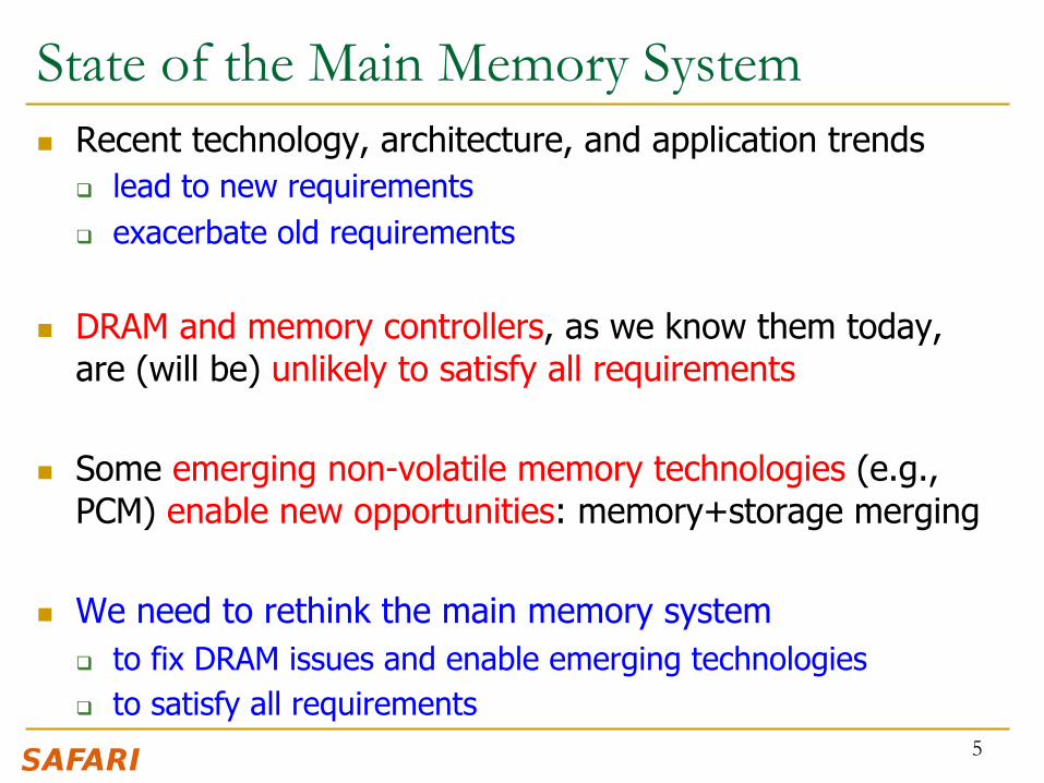
State of the Main Memory System n Recent technology, architecture, and application trends
q lead to new requirements q exacerbate old requirements
n DRAM and memory controllers, as we know them today, are (will be) unlikely to satisfy all requirements
n Some emerging non-volatile memory technologies (e.g., PCM) enable new opportunities: memory+storage merging
n We need to rethink the main memory system q to fix DRAM issues and enable emerging technologies q to satisfy all requirements
5
Agenda
n Major Trends Affecting Main Memory n DRAM Scaling Problem and Solution Directions n Three New Techniques for DRAM
q RAIDR: Reducing Refresh Impact q TL-DRAM: Reducing DRAM Latency q SALP: Reducing Bank Conflict Impact
n Ongoing Research n Summary
6

Major Trends Affecting Main Memory (I) n Need for main memory capacity, bandwidth, QoS increasing
n Main memory energy/power is a key system design concern
n DRAM technology scaling is ending
7

Major Trends Affecting Main Memory (II) n Need for main memory capacity, bandwidth, QoS increasing
q Multi-core: increasing number of cores q Data-intensive applications: increasing demand/hunger for data q Consolidation: cloud computing, GPUs, mobile
n Main memory energy/power is a key system design concern
n DRAM technology scaling is ending
8

Major Trends Affecting Main Memory (III) n Need for main memory capacity, bandwidth, QoS increasing
n Main memory energy/power is a key system design concern
q ~40-50% energy spent in off-chip memory hierarchy [Lefurgy, IEEE Computer 2003]
q DRAM consumes power even when not used (periodic refresh)
n DRAM technology scaling is ending
9

Major Trends Affecting Main Memory (IV) n Need for main memory capacity, bandwidth, QoS increasing
n Main memory energy/power is a key system design concern
n DRAM technology scaling is ending
q ITRS projects DRAM will not scale easily below X nm q Scaling has provided many benefits:
n higher capacity (density), lower cost, lower energy
10
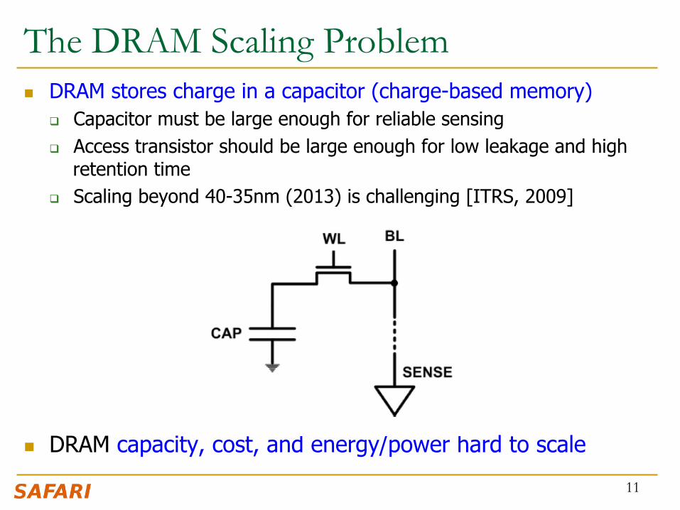
The DRAM Scaling Problem n DRAM stores charge in a capacitor (charge-based memory)
q Capacitor must be large enough for reliable sensing q Access transistor should be large enough for low leakage and high
retention time q Scaling beyond 40-35nm (2013) is challenging [ITRS, 2009]
n DRAM capacity, cost, and energy/power hard to scale
11

Solutions to the DRAM Scaling Problem
n Two potential solutions q Tolerate DRAM (by taking a fresh look at it) q Enable emerging memory technologies to eliminate/minimize
DRAM
n Do both q Hybrid memory systems
12

Solution 1: Tolerate DRAM n Overcome DRAM shortcomings with
q System-DRAM co-design q Novel DRAM architectures, interface, functions q Better waste management (efficient utilization)
n Key issues to tackle q Reduce refresh energy q Improve bandwidth and latency q Reduce waste q Enable reliability at low cost
n Liu, Jaiyen, Veras, Mutlu, “RAIDR: Retention-Aware Intelligent DRAM Refresh,” ISCA 2012. n Kim, Seshadri, Lee+, “A Case for Exploiting Subarray-Level Parallelism in DRAM,” ISCA 2012. n Lee+, “Tiered-Latency DRAM: A Low Latency and Low Cost DRAM Architecture,” HPCA 2013. n Liu+, “An Experimental Study of Data Retention Behavior in Modern DRAM Devices” ISCA’13. n Seshadri+, “RowClone: Fast and Efficient In-DRAM Copy and Initialization of Bulk Data,” 2013.
13
Solution 2: Emerging Memory Technologies n Some emerging resistive memory technologies seem more
scalable than DRAM (and they are non-volatile) n Example: Phase Change Memory
q Expected to scale to 9nm (2022 [ITRS]) q Expected to be denser than DRAM: can store multiple bits/cell
n But, emerging technologies have shortcomings as well q Can they be enabled to replace/augment/surpass DRAM?
n Lee, Ipek, Mutlu, Burger, “Architecting Phase Change Memory as a Scalable DRAM Alternative,” ISCA 2009, CACM 2010, Top Picks 2010.
n Meza, Chang, Yoon, Mutlu, Ranganathan, “Enabling Efficient and Scalable Hybrid Memories,” IEEE Comp. Arch. Letters 2012.
n Yoon, Meza et al., “Row Buffer Locality Aware Caching Policies for Hybrid Memories,” ICCD 2012 Best Paper Award.
14
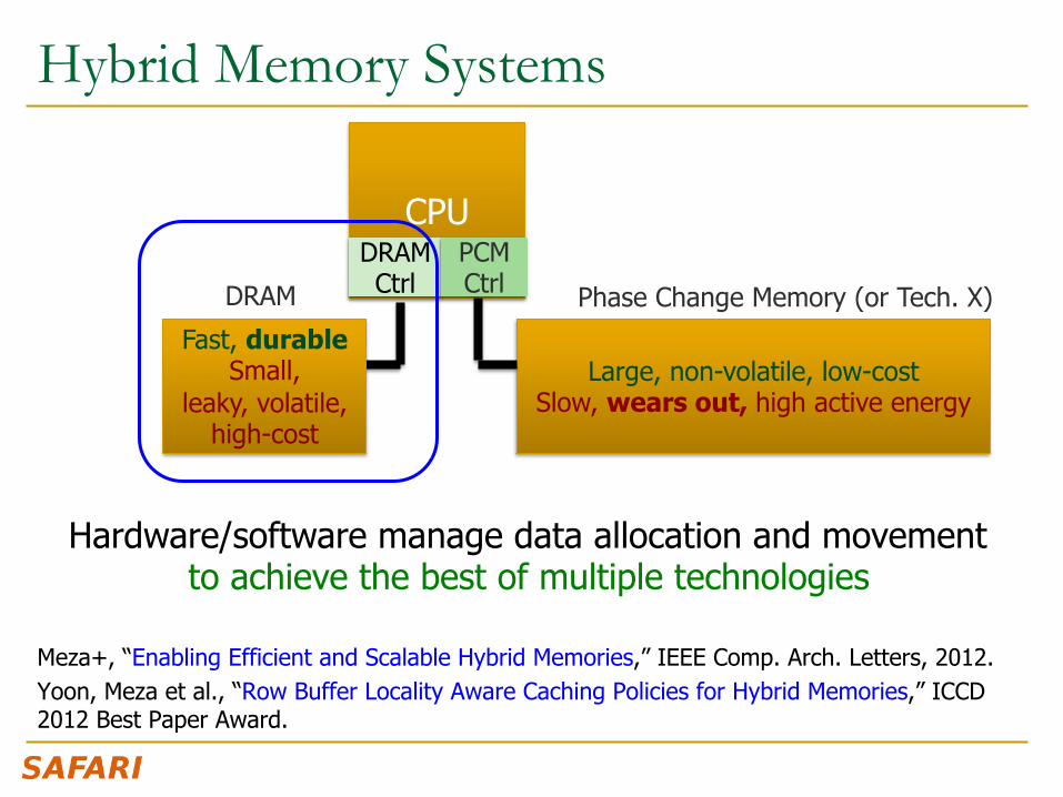
Hybrid Memory Systems
Meza+, “Enabling Efficient and Scalable Hybrid Memories,” IEEE Comp. Arch. Letters, 2012. Yoon, Meza et al., “Row Buffer Locality Aware Caching Policies for Hybrid Memories,” ICCD 2012 Best Paper Award.
CPU DRAMCtrl
Fast, durable Small,
leaky, volatile, high-cost
Large, non-volatile, low-cost Slow, wears out, high active energy
PCM Ctrl DRAM Phase Change Memory (or Tech. X)
Hardware/software manage data allocation and movement to achieve the best of multiple technologies

Agenda
n Major Trends Affecting Main Memory n DRAM Scaling Problem and Solution Directions n Three New Techniques for DRAM
q RAIDR: Reducing Refresh Impact q TL-DRAM: Reducing DRAM Latency q SALP: Reducing Bank Conflict Impact
n Ongoing Research n Summary
16

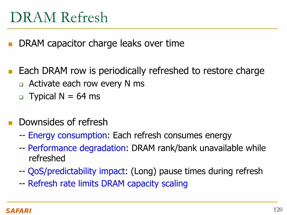
DRAM Refresh n DRAM capacitor charge leaks over time
n The memory controller needs to refresh each row periodically to restore charge q Activate + precharge each row every N ms q Typical N = 64 ms
n Downsides of refresh -- Energy consumption: Each refresh consumes energy
-- Performance degradation: DRAM rank/bank unavailable while refreshed
-- QoS/predictability impact: (Long) pause times during refresh -- Refresh rate limits DRAM density scaling 17

Refresh Today: Auto Refresh
18
Columns
Row
s
Row Buffer
DRAM CONTROLLER
DRAM Bus
BANK 0 BANK 1 BANK 2 BANK 3
A batch of rows are periodically refreshed via the auto-refresh command
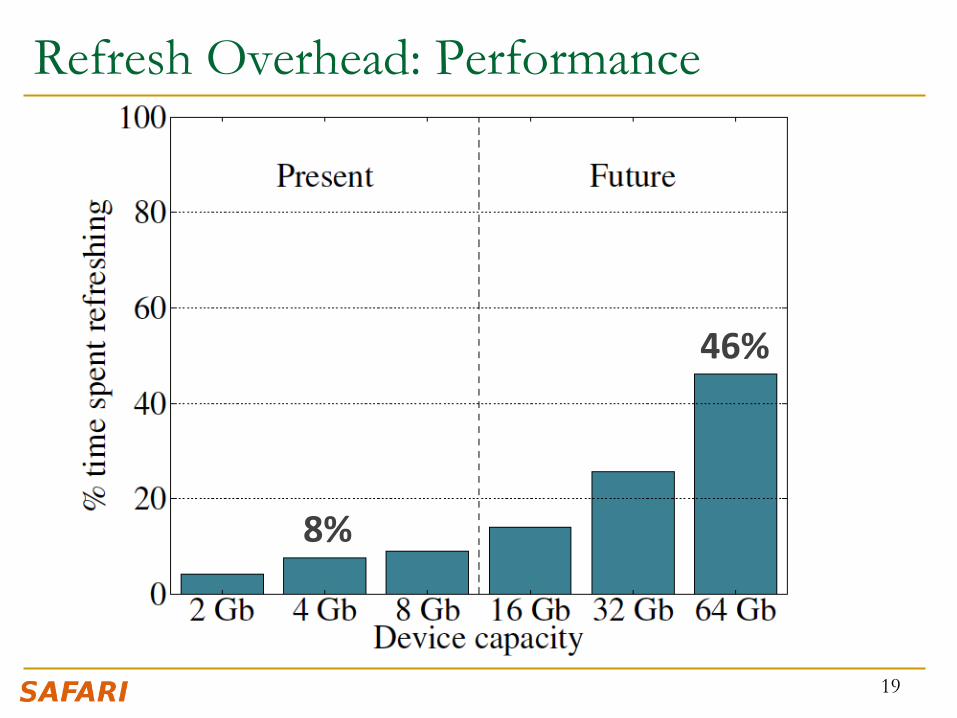
Refresh Overhead: Performance
19
8%
46%

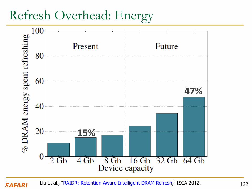
Refresh Overhead: Energy
20
15%
47%

Problem with Conventional Refresh n Today: Every row is refreshed at the same rate
n Observation: Most rows can be refreshed much less often without losing data [Kim+, EDL’09]
n Problem: No support in DRAM for different refresh rates per row
21

Retention Time of DRAM Rows n Observation: Only very few rows need to be refreshed at the
worst-case rate
n Can we exploit this to reduce refresh operations at low cost?
22

Reducing DRAM Refresh Operations n Idea: Identify the retention time of different rows and
refresh each row at the frequency it needs to be refreshed
n (Cost-conscious) Idea: Bin the rows according to their minimum retention times and refresh rows in each bin at the refresh rate specified for the bin q e.g., a bin for 64-128ms, another for 128-256ms, …
n Observation: Only very few rows need to be refreshed very frequently [64-128ms] à Have only a few bins à Low HW overhead to achieve large reductions in refresh operations
n Liu et al., “RAIDR: Retention-Aware Intelligent DRAM Refresh,” ISCA 2012.
23

1. Profiling: Profile the retention time of all DRAM rows à can be done at DRAM design time or dynamically 2. Binning: Store rows into bins by retention time à use Bloom Filters for efficient and scalable storage 3. Refreshing: Memory controller refreshes rows in different bins at different rates à probe Bloom Filters to determine refresh rate of a row
RAIDR: Mechanism
24
1.25KB storage in controller for 32GB DRAM memory

1. Profiling
25

2. Binning
n How to efficiently and scalably store rows into retention time bins?
n Use Hardware Bloom Filters [Bloom, CACM 1970]
26

Bloom Filter Operation Example
27

Bloom Filter Operation Example
28

Bloom Filter Operation Example
29

Bloom Filter Operation Example
30

Benefits of Bloom Filters as Bins n False positives: a row may be declared present in the
Bloom filter even if it was never inserted q Not a problem: Refresh some rows more frequently than
needed
n No false negatives: rows are never refreshed less frequently than needed (no correctness problems)
n Scalable: a Bloom filter never overflows (unlike a fixed-size table)
n Efficient: No need to store info on a per-row basis; simple hardware à 1.25 KB for 2 filters for 32 GB DRAM system
31

3. Refreshing (RAIDR Refresh Controller)
32

3. Refreshing (RAIDR Refresh Controller)
33
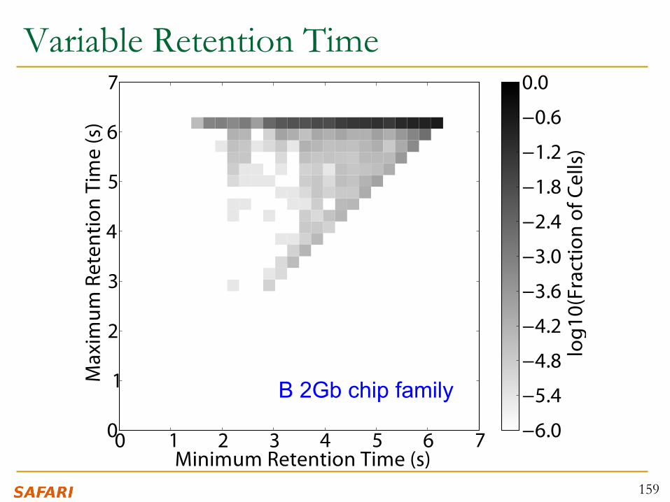
Liu et al., “RAIDR: Retention-Aware Intelligent DRAM Refresh,” ISCA 2012.

Tolerating Temperature Changes
34

RAIDR: Baseline Design
35
Refresh control is in DRAM in today’s auto-refresh systems RAIDR can be implemented in either the controller or DRAM
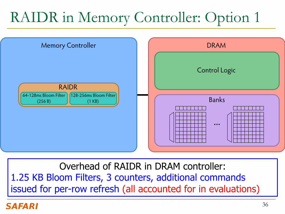
RAIDR in Memory Controller: Option 1
36
Overhead of RAIDR in DRAM controller: 1.25 KB Bloom Filters, 3 counters, additional commands issued for per-row refresh (all accounted for in evaluations)

RAIDR in DRAM Chip: Option 2
37
Overhead of RAIDR in DRAM chip: Per-chip overhead: 20B Bloom Filters, 1 counter (4 Gbit chip)
Total overhead: 1.25KB Bloom Filters, 64 counters (32 GB DRAM)

RAIDR Results n Baseline:
q 32 GB DDR3 DRAM system (8 cores, 512KB cache/core) q 64ms refresh interval for all rows
n RAIDR: q 64–128ms retention range: 256 B Bloom filter, 10 hash functions q 128–256ms retention range: 1 KB Bloom filter, 6 hash functions q Default refresh interval: 256 ms
n Results on SPEC CPU2006, TPC-C, TPC-H benchmarks q 74.6% refresh reduction q ~16%/20% DRAM dynamic/idle power reduction q ~9% performance improvement
38

RAIDR Refresh Reduction
39
32 GB DDR3 DRAM system
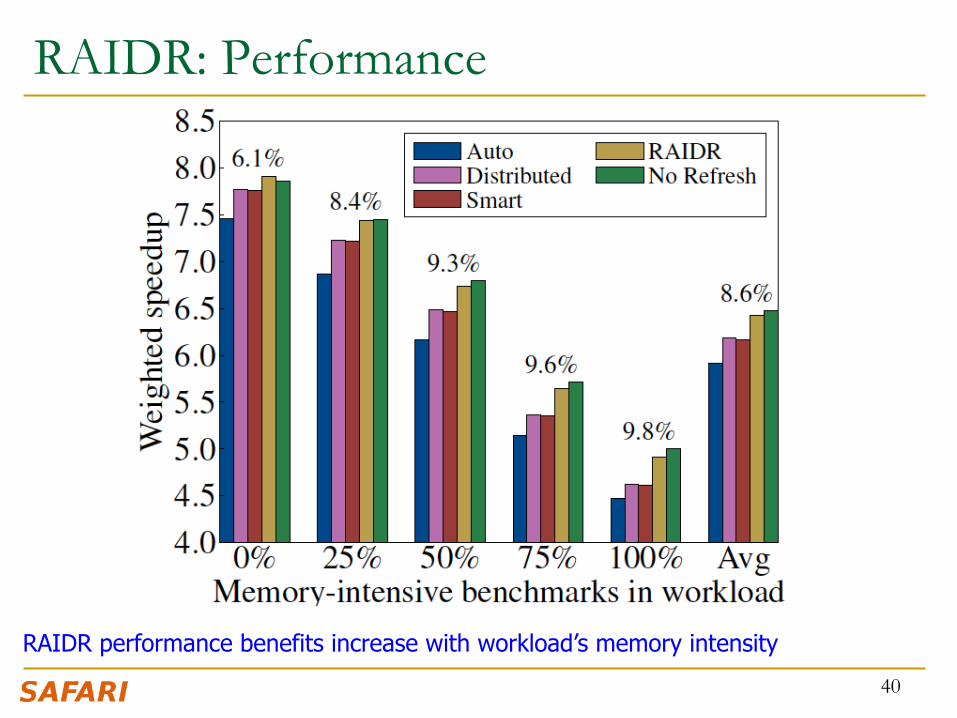
RAIDR: Performance
40
RAIDR performance benefits increase with workload’s memory intensity

RAIDR: DRAM Energy Efficiency
41
RAIDR energy benefits increase with memory idleness

DRAM Device Capacity Scaling: Performance
42
RAIDR performance benefits increase with DRAM chip capacity

DRAM Device Capacity Scaling: Energy
43
RAIDR energy benefits increase with DRAM chip capacity RAIDR slides

Agenda
n Major Trends Affecting Main Memory n DRAM Scaling Problem and Solution Directions n Three New Techniques for DRAM
q RAIDR: Reducing Refresh Impact q TL-DRAM: Reducing DRAM Latency q SALP: Reducing Bank Conflict Impact
n Ongoing Research n Summary
44

45
Historical DRAM Latency-‐Capacity Trend
0
20
40
60
80
100
0.0
0.5
1.0
1.5
2.0
2.5
2000 2003 2006 2008 2011
Latency (ns)
Capa
city (G
b)
Year
Capacity Latency (tRC)
16X
-‐20%
DRAM latency con.nues to be a cri.cal bo4leneck

46
What Causes the Long Latency? DRAM Chip
channel
I/O
channel
I/O
cell array cell array
banks subarray
subarray
row decod
er
sense amplifier
capacitor
access transistor
wordline
bitline
cell

47
DRAM Chip
channel
I/O
channel
I/O
cell array cell array
banks subarray
subarray What Causes the Long Latency?
DRAM Latency = Subarray Latency + I/O Latency DRAM Latency = Subarray Latency + I/O Latency
Dominant
Suba
rray
I/O
row add
r.
row decoder
sense am
plifier
mux column addr.
48
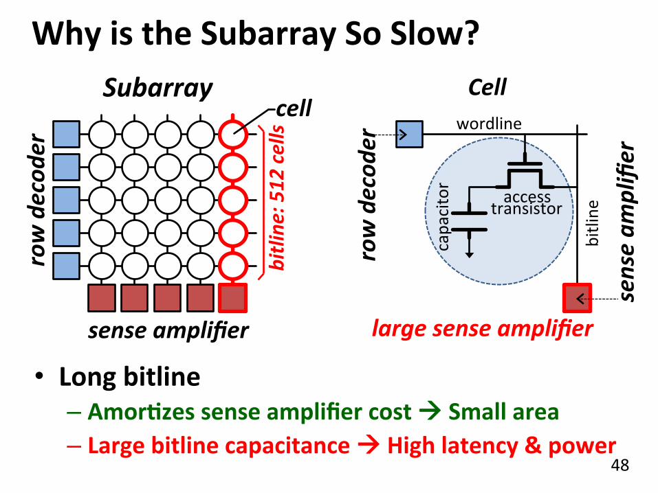
Why is the Subarray So Slow? Subarray
row decod
er
sense amplifier
capacitor
access transistor
wordline
bitline
Cell
large sense amplifier
bitline
: 512 cells cell
• Long bitline – AmorRzes sense amplifier cost à Small area – Large bitline capacitance à High latency & power
sense am
plifier
row decod
er

49
Trade-‐Off: Area (Die Size) vs. Latency
Faster
Smaller
Short Bitline
Long Bitline
Trade-‐Off: Area vs. Latency

50
Trade-‐Off: Area (Die Size) vs. Latency
0
1
2
3
4
0 10 20 30 40 50 60 70
Normalized
DRA
M Area
Latency (ns)
64
32
128 256 512 cells/bitline
Commodity DRAM
Long Bitline
Cheape
r
Faster
Fancy DRAM Short Bitline

51
Short Bitline
Low Latency
ApproximaRng the Best of Both Worlds Long Bitline
Small Area
Long Bitline
Low Latency
Short Bitline Our Proposal Small Area
Short Bitline è Fast Need
IsolaJon Add IsolaJon Transistors
High Latency
Large Area

52
ApproximaRng the Best of Both Worlds
Low Latency
Our Proposal Small Area
Long Bitline Small Area
Long Bitline
High Latency
Short Bitline
Low Latency
Short Bitline Large Area
Tiered-‐Latency DRAM
Low Latency
Small area using long bitline

53
Tiered-‐Latency DRAM
Near Segment
Far Segment
IsolaJon Transistor
• Divide a bitline into two segments with an isolaRon transistor
Sense Amplifier

54
Far Segment Far Segment
Near Segment Access
Near Segment
IsolaJon Transistor
• Turn off the isolaRon transistor
IsolaJon Transistor (off)
Sense Amplifier
Reduced bitline capacitance è Low latency & low power
Reduced bitline length

55
Near Segment Near Segment
Far Segment Access • Turn on the isolaRon transistor
Far Segment
IsolaJon Transistor IsolaJon Transistor (on)
Sense Amplifier
Large bitline capacitance AddiRonal resistance of isolaRon transistor
Long bitline length
è High latency & high power
56
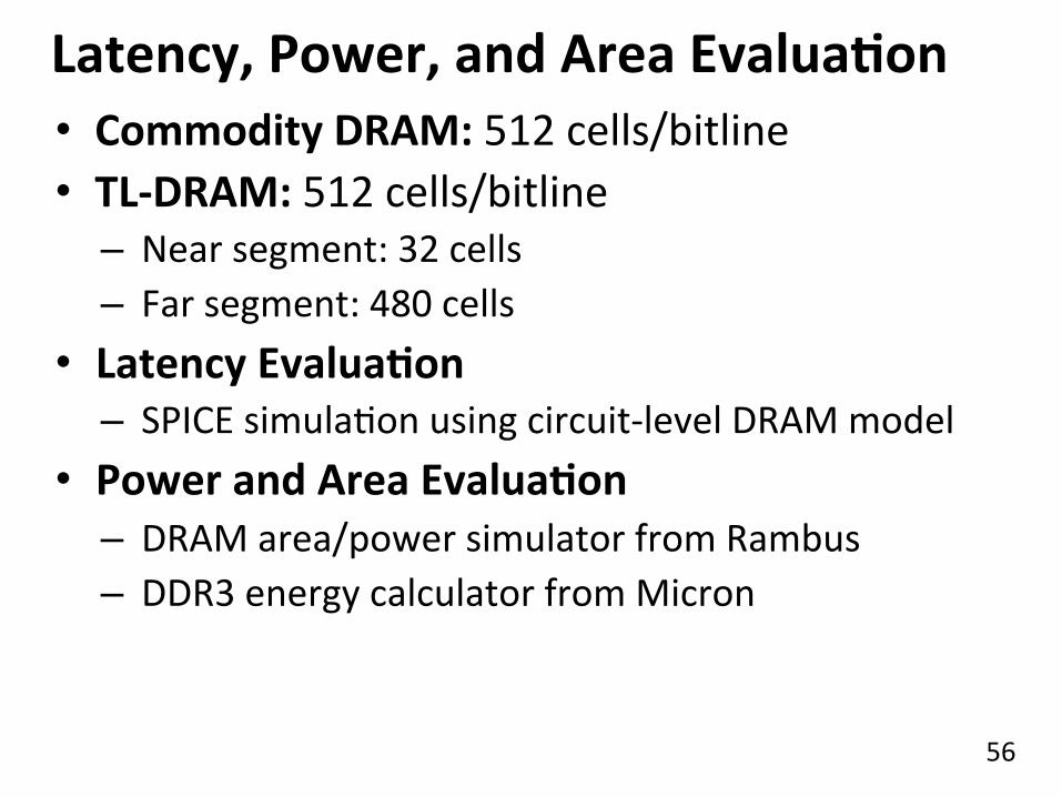
Latency, Power, and Area EvaluaRon • Commodity DRAM: 512 cells/bitline • TL-‐DRAM: 512 cells/bitline
– Near segment: 32 cells – Far segment: 480 cells
• Latency EvaluaRon – SPICE simulaOon using circuit-‐level DRAM model
• Power and Area EvaluaRon – DRAM area/power simulator from Rambus – DDR3 energy calculator from Micron
57
0%
50%
100%
150%
0%
50%
100%
150%
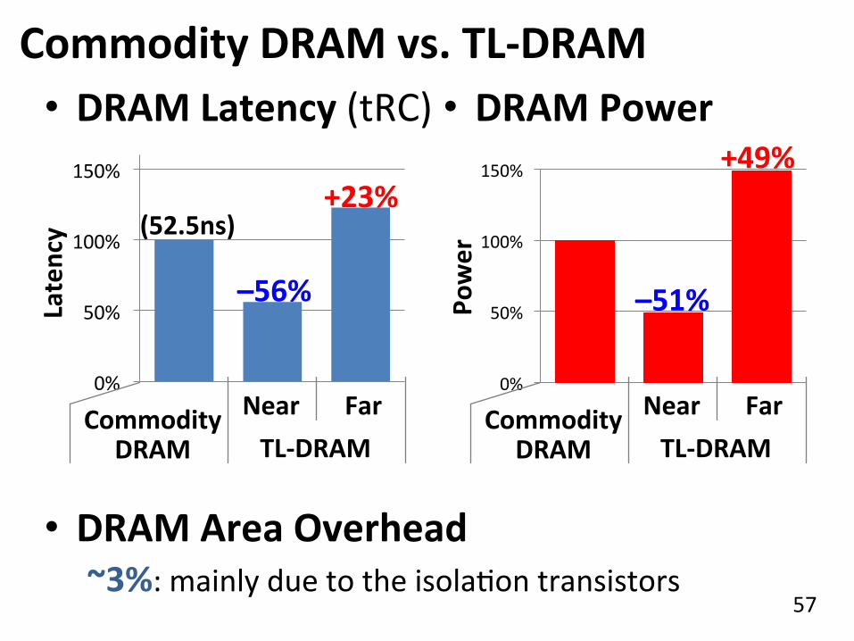
Commodity DRAM vs. TL-‐DRAM Latency
Power
–56%
+23%
–51%
+49% • DRAM Latency (tRC) • DRAM Power
• DRAM Area Overhead ~3%: mainly due to the isolaOon transistors
TL-‐DRAM Commodity
DRAM Near Far Commodity
DRAM Near Far TL-‐DRAM
(52.5ns)
58
Latency vs. Near Segment Length
0
20
40
60
80
1 2 4 8 16 32 64 128 256 512
Near Segment Length (Cells) Ref.
Near Segment Far Segment
Latency (ns)
Longer near segment length leads to higher near segment latency

59
Latency vs. Near Segment Length
0
20
40
60
80
1 2 4 8 16 32 64 128 256 512
Near Segment Length (Cells) Ref.
Near Segment Far Segment
Latency (ns)
Far segment latency is higher than commodity DRAM latency
Far Segment Length = 512 – Near Segment Length

60
Trade-‐Off: Area (Die-‐Area) vs. Latency
0
1
2
3
4
0 10 20 30 40 50 60 70
Normalized
DRA
M Area
Latency (ns)
64
32
128 256 512 cells/bitline
Cheape
r
Faster
Near Segment Far Segment
61
Leveraging Tiered-‐Latency DRAM • TL-‐DRAM is a substrate that can be leveraged by the hardware and/or soVware
• Many potenOal uses 1. Use near segment as hardware-‐managed inclusive cache to far segment
2. Use near segment as hardware-‐managed exclusive cache to far segment
3. Profile-‐based page mapping by operaOng system 4. Simply replace DRAM with TL-‐DRAM
62
subarray
Near Segment as Hardware-‐Managed Cache TL-‐DRAM
I/O
cache
main memory
• Challenge 1: How to efficiently migrate a row between segments?
• Challenge 2: How to efficiently manage the cache?
far segment near segment sense amplifier
channel

63
Inter-‐Segment MigraRon
Near Segment
Far Segment
IsolaJon Transistor
Sense Amplifier
Source
DesJnaJon
• Goal: Migrate source row into desOnaOon row • Naïve way: Memory controller reads the source row byte by byte and writes to desOnaOon row byte by byte
→ High latency

64
Inter-‐Segment MigraRon • Our way:
– Source and desOnaOon cells share bitlines – Transfer data from source to desOnaOon across shared bitlines concurrently
Near Segment
Far Segment
IsolaJon Transistor
Sense Amplifier
Source
DesJnaJon

65
Inter-‐Segment MigraRon
Near Segment
Far Segment
IsolaJon Transistor
Sense Amplifier
• Our way: – Source and desOnaOon cells share bitlines – Transfer data from source to desOnaOon across shared bitlines concurrently
Step 2: AcOvate desOnaOon row to connect cell and bitline
Step 1: AcOvate source row
AddiRonal ~4ns over row access latency MigraRon is overlapped with source row access

66
subarray
Near Segment as Hardware-‐Managed Cache TL-‐DRAM
I/O
cache
main memory
• Challenge 1: How to efficiently migrate a row between segments?
• Challenge 2: How to efficiently manage the cache?
far segment near segment sense amplifier
channel
67
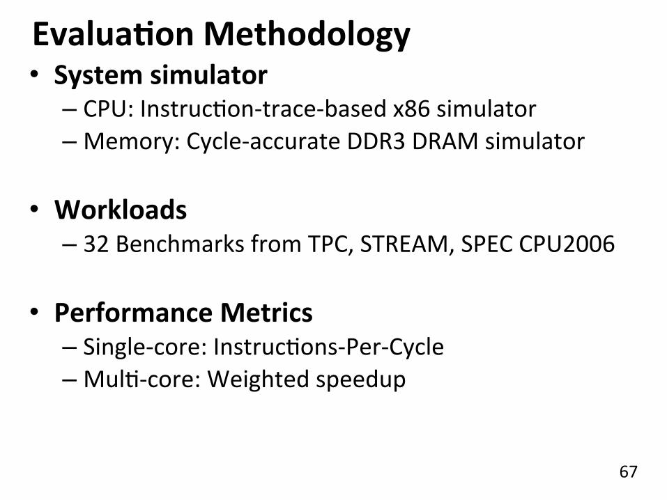
EvaluaRon Methodology • System simulator
– CPU: InstrucOon-‐trace-‐based x86 simulator – Memory: Cycle-‐accurate DDR3 DRAM simulator
• Workloads – 32 Benchmarks from TPC, STREAM, SPEC CPU2006
• Performance Metrics – Single-‐core: InstrucOons-‐Per-‐Cycle – MulO-‐core: Weighted speedup

68
ConfiguraRons • System configuraRon
– CPU: 5.3GHz – LLC: 512kB private per core – Memory: DDR3-‐1066
• 1-‐2 channel, 1 rank/channel • 8 banks, 32 subarrays/bank, 512 cells/bitline • Row-‐interleaved mapping & closed-‐row policy
• TL-‐DRAM configuraRon – Total bitline length: 512 cells/bitline – Near segment length: 1-‐256 cells – Hardware-‐managed inclusive cache: near segment

69
0%
20%
40%
60%
80%
100%
120%
1 (1-‐ch) 2 (2-‐ch) 4 (4-‐ch) 0%
20%
40%
60%
80%
100%
120%
1 (1-‐ch) 2 (2-‐ch) 4 (4-‐ch)
Performance & Power ConsumpRon 11.5%
Normalized
Perform
ance
Core-‐Count (Channel) Normalized
Pow
er Core-‐Count (Channel)
10.7%
12.4% –23%
–24%
–26%
Using near segment as a cache improves performance and reduces power consumpJon
70
0% 2% 4% 6% 8% 10% 12% 14%
1 2 4 8 16 32 64 128 256
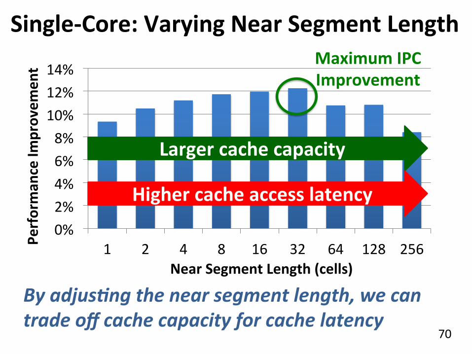
Single-‐Core: Varying Near Segment Length
By adjusJng the near segment length, we can trade off cache capacity for cache latency
Larger cache capacity
Higher cache access latency
Maximum IPC Improvement
Perform
ance Im
provem
ent
Near Segment Length (cells)

71
Other Mechanisms & Results • More mechanisms for leveraging TL-‐DRAM
– Hardware-‐managed exclusive caching mechanism – Profile-‐based page mapping to near segment – TL-‐DRAM improves performance and reduces power consumpOon with other mechanisms
• More than two Rers – Latency evaluaOon for three-‐Oer TL-‐DRAM
• Detailed circuit evaluaRon for DRAM latency and power consumpOon – ExaminaOon of tRC and tRCD
• ImplementaRon details and storage cost analysis in memory controller

72
Summary of TL-‐DRAM • Problem: DRAM latency is a criRcal performance bokleneck • Our Goal: Reduce DRAM latency with low area cost • ObservaRon: Long bitlines in DRAM are the dominant source of DRAM latency
• Key Idea: Divide long bitlines into two shorter segments – Fast and slow segments
• Tiered-‐latency DRAM: Enables latency heterogeneity in DRAM – Can leverage this in many ways to improve performance and reduce power consumpRon
• Results: When the fast segment is used as a cache to the slow segment à Significant performance improvement (>12%) and power reducOon (>23%) at low area cost (3%)

Agenda
n Major Trends Affecting Main Memory n DRAM Scaling Problem and Solution Directions n Three New Techniques for DRAM
q RAIDR: Reducing Refresh Impact q TL-DRAM: Reducing DRAM Latency q SALP: Reducing Bank Conflict Impact
n Ongoing Research n Summary
73

The Memory Bank Conflict Problem
n Two requests to the same bank are serviced serially n Problem: Costly in terms of performance and power n Goal: We would like to reduce bank conflicts without
increasing the number of banks (at low cost)
n Idea: Exploit the internal sub-array structure of a DRAM bank to parallelize bank conflicts q By reducing global sharing of hardware between sub-arrays
n Kim, Seshadri, Lee, Liu, Mutlu, “A Case for Exploiting Subarray-Level Parallelism in DRAM,” ISCA 2012.
74

75
.me Wr Rd
Wr Rd .me
Bank
.me
Bank
Bank
• Two Banks
• One Bank
1. Serializa.on
Wr Wr Rd Rd Wr 2 Wr 2 Rd Rd Wr 2 Wr 2 Rd Rd 3 3 3
2. Write Penalty 3. Thrashing Row-‐Buffer
Served in parallel
Wasted
The Problem with Memory Bank Conflicts
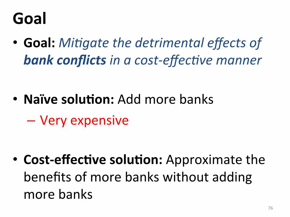
Goal • Goal: Mi.gate the detrimental effects of bank conflicts in a cost-‐effec.ve manner
• Naïve soluRon: Add more banks – Very expensive
• Cost-‐effecRve soluRon: Approximate the benefits of more banks without adding more banks
76

A DRAM bank is divided into subarrays Key ObservaRon #1
77
Row
Row-‐Buffer
Row Row Row
32k rows
Logical Bank
A single row-‐buffer cannot drive all rows
Global Row-‐Buf
Physical Bank
Local Row-‐Buf
Local Row-‐Buf Subarray1
Subarray64
Many local row-‐buffers, one at each subarray

Key ObservaRon #2 Each subarray is mostly independent…
– except occasionally sharing global structures
78
Global Row-‐Buf
Glob
al Decod
er
Bank
Local Row-‐Buf
Local Row-‐Buf Subarray1
Subarray64
·∙·∙·∙
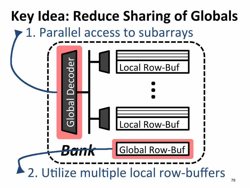
Key Idea: Reduce Sharing of Globals
79
Global Row-‐Buf
Glob
al Decod
er
Bank
Local Row-‐Buf
Local Row-‐Buf
·∙·∙·∙
1. Parallel access to subarrays
2. UOlize mulOple local row-‐buffers

Overview of Our Mechanism
80
·∙·∙·∙
Req Req
Global Row-‐Buf
Local Row-‐Buf
Req
Local Row-‐Buf
Req 1. Parallelize
2. U.lize mul.ple local row-‐buffers
Subarray64
Subarray1 To same bank... but diff. subarrays

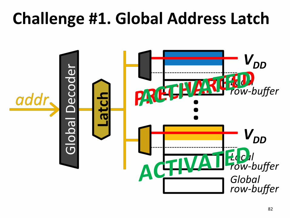
Challenges: Global Structures 1. Global Address Latch
2. Global Bitlines
81
Local row-‐buffer
Local row-‐buffer Global row-‐buffer
Challenge #1. Global Address Latch
82 ·∙·∙·∙ addr
VDD
addr
Glob
al Decod
er
VDD
Latch
Latch
Latch PRECHAR
GED
ACTIVATED
ACTIVATED
Local row-‐buffer
Local row-‐buffer Global row-‐buffer
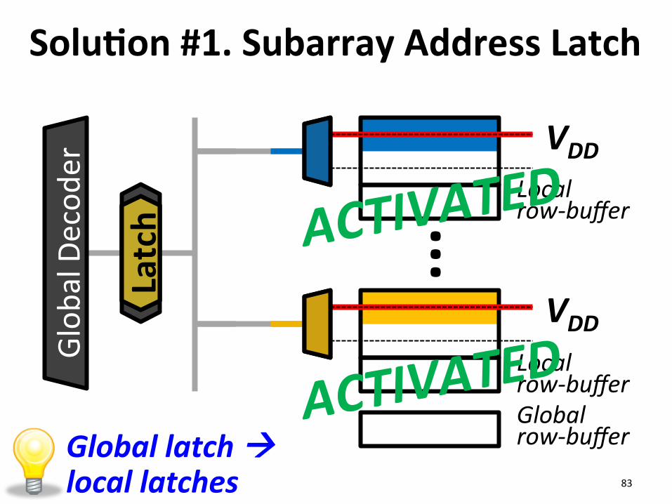
SoluRon #1. Subarray Address Latch
83
·∙·∙·∙
VDD
Glob
al Decod
er
VDD
Latch
Latch
Latch ACTIVATE
D
ACTIVATED
Global latch à local latches

Challenges: Global Structures 1. Global Address Latch
• Problem: Only one raised wordline • SoluOon: Subarray Address Latch
2. Global Bitlines
84
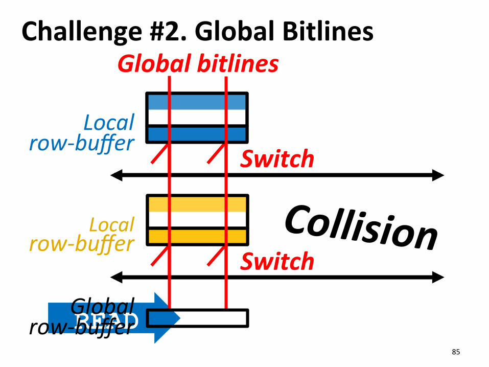
Challenge #2. Global Bitlines
85
Local row-‐buffer
Local row-‐buffer
Switch
Switch
READ
Global bitlines
Global row-‐buffer
Collision

Wire
SoluRon #2. Designated-‐Bit Latch
86
Global bitlines
Global row-‐buffer
Local row-‐buffer
Local row-‐buffer
Switch
Switch
READ READ
D D
D D
SelecJvely connect local to global

Challenges: Global Structures 1. Global Address Latch
• Problem: Only one raised wordline • SoluOon: Subarray Address Latch
2. Global Bitlines • Problem: Collision during access • SoluOon: Designated-‐Bit Latch
87 MASA (MulRtude of AcRvated Subarrays)

• Baseline (Subarray-‐Oblivious)
• MASA
MASA: Advantages
88
.me Wr 2 Wr 2 Rd Rd 3 3 3
1. Serializa.on
2. Write Penalty 3. Thrashing
.me Wr
Wr
Rd
Rd
Saved

MASA: Overhead • DRAM Die Size: Only 0.15% increase
– Subarray Address Latches – Designated-‐Bit Latches & Wire
• DRAM StaRc Energy: Small increase – 0.56mW for each acOvated subarray – But saves dynamic energy
• Controller: Small addiOonal storage – Keep track of subarray status (< 256B) – Keep track of new Oming constraints
89

Cheaper Mechanisms
90
D
D
Latches
1. SerializaO
on
2. W
r-‐Pe
nalty
3. Thrashing
MASA
SALP-‐2
SALP-‐1

System ConfiguraRon • System ConfiguraRon
– CPU: 5.3GHz, 128 ROB, 8 MSHR – LLC: 512kB per-‐core slice
• Memory ConfiguraRon – DDR3-‐1066 – (default) 1 channel, 1 rank, 8 banks, 8 subarrays-‐per-‐bank – (sensi.vity) 1-‐8 chans, 1-‐8 ranks, 8-‐64 banks, 1-‐128 subarrays
• Mapping & Row-‐Policy – (default) Line-‐interleaved & Closed-‐row – (sensi.vity) Row-‐interleaved & Open-‐row
• DRAM Controller ConfiguraRon – 64-‐/64-‐entry read/write queues per-‐channel – FR-‐FCFS, batch scheduling for writes
91
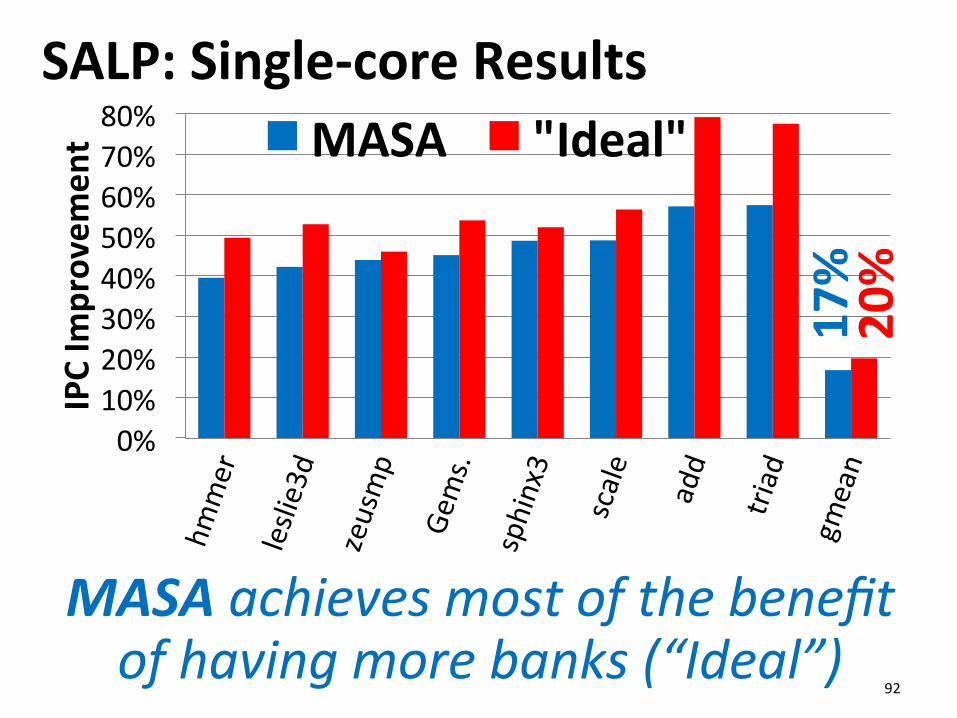
SALP: Single-‐core Results
92
0% 10% 20% 30% 40% 50% 60% 70% 80%
IPC Im
provem
ent MASA "Ideal"
17%
20%
MASA achieves most of the benefit of having more banks (“Ideal”)
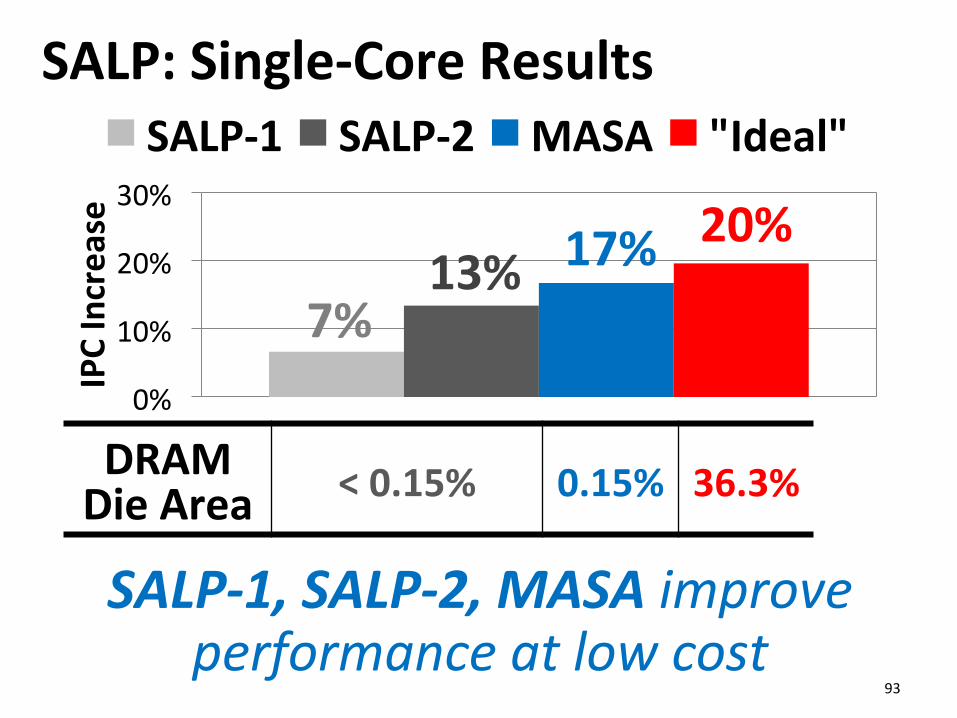
SALP: Single-‐Core Results
93
0%
10%
20%
30%
IPC Increase
SALP-‐1 SALP-‐2 MASA "Ideal"
SALP-‐1, SALP-‐2, MASA improve performance at low cost
20% 17% 13% 7%
DRAM Die Area < 0.15% 0.15% 36.3%
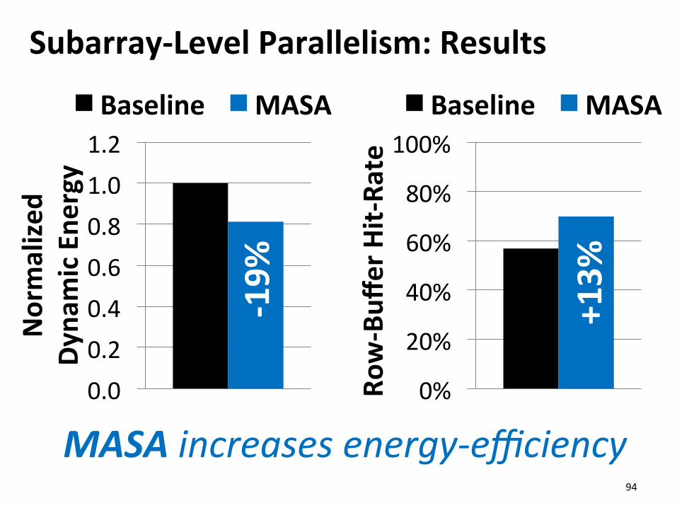
Subarray-‐Level Parallelism: Results
94
0.0 0.2 0.4 0.6 0.8 1.0 1.2
Normalized
Dy
namic Ene
rgy
Baseline MASA
0%
20%
40%
60%
80%
100%
Row-‐Buff
er Hit-‐Ra
te
Baseline MASA
MASA increases energy-‐efficiency
-‐19%
+13%
Agenda
n Major Trends Affecting Main Memory n DRAM Scaling Problem and Solution Directions n Three New Techniques for DRAM
q RAIDR: Reducing Refresh Impact q TL-DRAM: Reducing DRAM Latency q SALP: Reducing Bank Conflict Impact
n Ongoing Research n Summary
95

Sampling of Ongoing Research
n Online retention time profiling q Preliminary work in ISCA 2013 q Jamie Liu, Ben Jaiyen, Yoongu Kim, Chris Wilkerson, and Onur Mutlu,
"An Experimental Study of Data Retention Behavior in Modern DRAM Devices: Implications for Retention Time Profiling Mechanisms" Proceedings of the 40th International Symposium on Computer Architecture (ISCA), Tel-Aviv, Israel, June 2013. Slides (pptx) Slides (pdf)
n Fast bulk data copy and initialization: RowClone
n Refresh/demand parallelization
96

RowClone: Fast Bulk Data Copy and Initialization
Vivek Seshadri, Yoongu Kim, Chris Fallin, Donghyuk Lee, Rachata Ausavarungnirun, Gennady Pekhimenko, Yixin Luo, Onur Mutlu, Phillip B. Gibbons, Michael A. Kozuch, Todd C. Mowry,
"RowClone: Fast and Efficient In-DRAM Copy and Initialization of Bulk Data" CMU Computer Science Technical Report, CMU-CS-13-108, Carnegie Mellon University, April 2013.
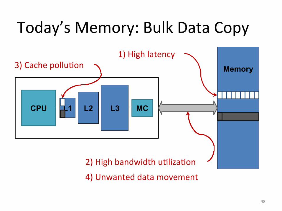
Today’s Memory: Bulk Data Copy
Memory
MC L3 L2 L1 CPU
1) High latency
2) High bandwidth uOlizaOon
3) Cache polluOon
4) Unwanted data movement
98

Future: RowClone (In-‐Memory Copy)
Memory
MC L3 L2 L1 CPU
1) Low latency
2) Low bandwidth uOlizaOon
3) No cache polluOon
4) No unwanted data movement
99 Seshadri et al., “RowClone: Fast and Efficient In-DRAM Copy and Initialization of Bulk Data,” CMU Tech Report 2013.
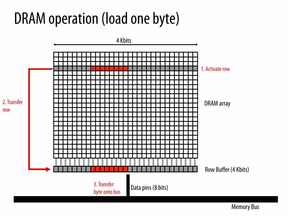
DRAM operation (load one byte)
Row Buffer (4 Kbits)
Memory Bus
Data pins (8 bits)
DRAM array
4 Kbits
1. Activate row
2. Transfer row
3. Transfer byte onto bus
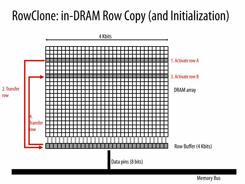
RowClone: in-DRAM Row Copy (and Initialization)
Row Buffer (4 Kbits)
Memory Bus
Data pins (8 bits)
DRAM array
4 Kbits
1. Activate row A
2. Transfer row
3. Activate row B
4. Transfer row

Our Approach: Key Idea
• DRAM banks contain 1. MuOple rows of DRAM cells – row = 8KB 2. A row buffer shared by the DRAM rows
• Large scale copy 1. Copy data from source row to row buffer 2. Copy data from row buffer to desOnaOon row
102

DRAM Subarray Microarchitecture
wordline
DRAM Cell
DRAM Row (share wordline)
(~8Kb)
Sense Amplifiers (row buffer)
103

DRAM OperaOon
0 1 0 0 1 1 0 0 0 1 1 0
AcOvate (src) Precharge
0 1 0 0 1 1 0 0 0 1 1 0
? ? ? ? ? ? ? ? ? ? ? ?
1 1 0 1 0 1 1 1 0 0 1 1
Raise wordline
Sense Amplifiers (row buffer)
src
dst
- + - - + + - - - + + -
104

RowClone: Intra-‐subarray Copy
0 1 0 0 1 1 0 0 0 1 1 0
1 1 0 1 0 1 1 1 0 0 1 1
AcOvate (src) DeacOvate (our proposal) AcOvate (dst)
0 1 0 0 1 1 0 0 0 1 1 0
? ? ? ? ? ? ? ? ? ? ? ? 0 1 0 0 1 1 0 0 0 1 1 0
Sense Amplifiers (row buffer)
src
dst
105

RowClone: Inter-‐bank Copy
I/O Bus Transfer
(our proposal)
src
dst
Read Write
106

RowClone: Inter-‐subarray Copy
I/O Bus 1. Transfer (src to temp)
src
dst
temp
2. Transfer (temp to dst) 107
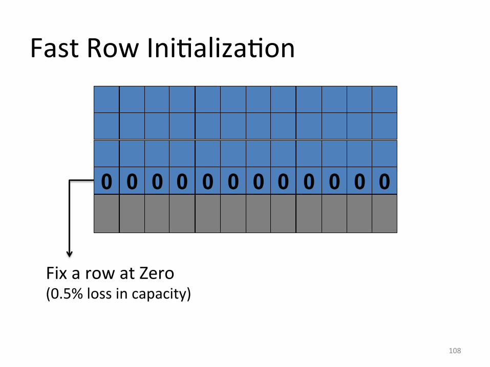
Fast Row IniOalizaOon
0 0 0 0 0 0 0 0 0 0 0 0
Fix a row at Zero (0.5% loss in capacity)
108

RowClone: Latency and Energy Savings
0
0.2
0.4
0.6
0.8
1
1.2
Latency Energy
Normalized
Savings
Baseline Intra-‐Subarray Inter-‐Bank Inter-‐Subarray
11.5x 74x
109 Seshadri et al., “RowClone: Fast and Efficient In-DRAM Copy and Initialization of Bulk Data,” CMU Tech Report 2013.

Agenda
n Major Trends Affecting Main Memory n DRAM Scaling Problem and Solution Directions n Three New Techniques for DRAM
q RAIDR: Reducing Refresh Impact q TL-DRAM: Reducing DRAM Latency q SALP: Reducing Bank Conflict Impact
n Ongoing Research n Summary
110
Summary n Three major problems with DRAM scaling and design:
high refresh rate, high latency, low parallelism
n Four new DRAM designs q RAIDR: Reduces refresh impact q TL-DRAM: Reduces DRAM latency at low cost q SALP: Improves DRAM parallelism q RowClone: Accelerates page copy and initialization
n All four designs q Improve both performance and energy consumption q Are low cost (low DRAM area overhead) q Enable new degrees of freedom to software & controllers
n Rethinking DRAM interface and design essential for scaling q Co-design DRAM with the rest of the system
111
Thank you.
112

A Fresh Look at DRAM Architecture: New Techniques to Improve DRAM
Latency, Parallelism, and Energy Efficiency
Onur Mutlu [email protected]
July 4, 2013 INRIA
Additional Material
114

1 Carnegie Mellon University 2 Intel Corporation
Jamie Liu1 Ben Jaiyen1 Yoongu Kim1 Chris Wilkerson2 Onur Mutlu1
An Experimental Study of Data Retention Behavior
in Modern DRAM Devices
Implications for Retention Time Profiling Mechanisms

Summary (I) n DRAM requires periodic refresh to avoid data loss
q Refresh wastes energy, reduces performance, limits DRAM density scaling n Many past works observed that different DRAM cells can retain data for
different times without being refreshed; proposed reducing refresh rate for strong DRAM cells q Problem: These techniques require an accurate profile of the retention time of
all DRAM cells
n Our goal: To analyze the retention time behavior of DRAM cells in modern DRAM devices to aid the collection of accurate profile information
n Our experiments: We characterize 248 modern commodity DDR3 DRAM chips from 5 manufacturers using an FPGA based testing platform
n Two Key Issues: 1. Data Pattern Dependence: A cell’s retention time is heavily dependent on data values stored in itself and nearby cells, which cannot easily be controlled. 2. Variable Retention Time: Retention time of some cells change unpredictably from high to low at large timescales.

Summary (II) n Key findings on Data Pattern Dependence
q There is no observed single data pattern that elicits the lowest retention times for a DRAM device à very hard to find this pattern
q DPD varies between devices due to variation in DRAM array circuit design between manufacturers
q DPD of retention time gets worse as DRAM scales to smaller feature sizes
n Key findings on Variable Retention Time q VRT is common in modern DRAM cells that are weak q The timescale at which VRT occurs is very large (e.g., a cell can stay
in high retention time state for a day or longer) à finding minimum retention time can take very long
n Future work on retention time profiling must address these issues
117

Talk Agenda n DRAM Refresh: Background and Motivation n Challenges and Our Goal n DRAM Characterization Methodology n Foundational Results
q Temperature Dependence q Retention Time Distribution
n Data Pattern Dependence: Analysis and Implications n Variable Retention Time: Analysis and Implications n Conclusions
118
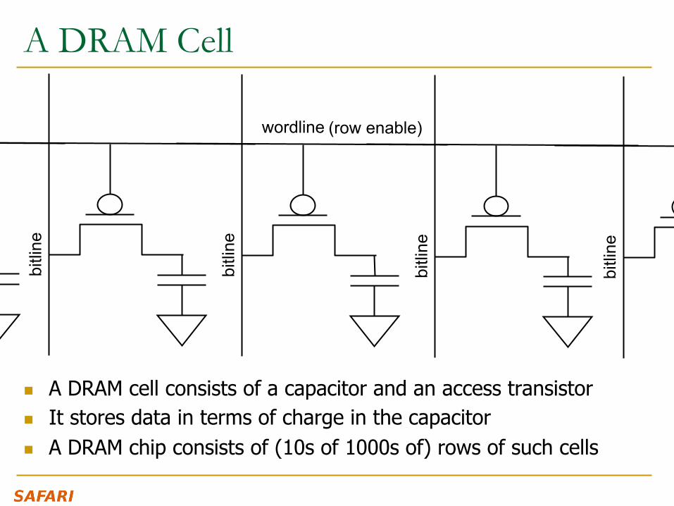
A DRAM Cell
n A DRAM cell consists of a capacitor and an access transistor n It stores data in terms of charge in the capacitor n A DRAM chip consists of (10s of 1000s of) rows of such cells
wordline
bitli
ne
bitli
ne
bitli
ne
bitli
ne
bitli
ne
(row enable)
DRAM Refresh
n DRAM capacitor charge leaks over time
n Each DRAM row is periodically refreshed to restore charge q Activate each row every N ms q Typical N = 64 ms
n Downsides of refresh -- Energy consumption: Each refresh consumes energy
-- Performance degradation: DRAM rank/bank unavailable while refreshed
-- QoS/predictability impact: (Long) pause times during refresh -- Refresh rate limits DRAM capacity scaling
120

Refresh Overhead: Performance
121
8%
46%
Liu et al., “RAIDR: Retention-Aware Intelligent DRAM Refresh,” ISCA 2012.
Refresh Overhead: Energy
122
15%
47%
Liu et al., “RAIDR: Retention-Aware Intelligent DRAM Refresh,” ISCA 2012.

Previous Work on Reducing Refreshes n Observed significant variation in data retention times of
DRAM cells (due to manufacturing process variation) q Retention time: maximum time a cell can go without being
refreshed while maintaining its stored data
n Proposed methods to take advantage of widely varying retention times among DRAM rows q Reduce refresh rate for rows that can retain data for longer
than 64 ms, e.g., [Liu+ ISCA 2012]
q Disable rows that have low retention times, e.g., [Venkatesan+ HPCA 2006]
n Showed large benefits in energy and performance
123
1. Profiling: Profile the retention time of all DRAM rows 2. Binning: Store rows into bins by retention time à use Bloom Filters for efficient and scalable storage 3. Refreshing: Memory controller refreshes rows in different bins at different rates à probe Bloom Filters to determine refresh rate of a row
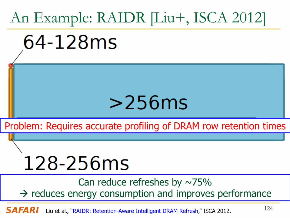
An Example: RAIDR [Liu+, ISCA 2012]
124
1.25KB storage in controller for 32GB DRAM memory
Can reduce refreshes by ~75% à reduces energy consumption and improves performance
Problem: Requires accurate profiling of DRAM row retention times
Liu et al., “RAIDR: Retention-Aware Intelligent DRAM Refresh,” ISCA 2012.
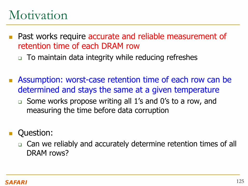
Motivation n Past works require accurate and reliable measurement of
retention time of each DRAM row q To maintain data integrity while reducing refreshes
n Assumption: worst-case retention time of each row can be determined and stays the same at a given temperature q Some works propose writing all 1’s and 0’s to a row, and
measuring the time before data corruption
n Question: q Can we reliably and accurately determine retention times of all
DRAM rows?
125

Talk Agenda n DRAM Refresh: Background and Motivation n Challenges and Our Goal n DRAM Characterization Methodology n Foundational Results
q Temperature Dependence q Retention Time Distribution
n Data Pattern Dependence: Analysis and Implications n Variable Retention Time: Analysis and Implications n Conclusions
126

Two Challenges to Retention Time Profiling n Data Pattern Dependence (DPD) of retention time
n Variable Retention Time (VRT) phenomenon
127

Two Challenges to Retention Time Profiling n Challenge 1: Data Pattern Dependence (DPD)
q Retention time of a DRAM cell depends on its value and the values of cells nearby it
q When a row is activated, all bitlines are perturbed simultaneously
128

n Electrical noise on the bitline affects reliable sensing of a DRAM cell n The magnitude of this noise is affected by values of nearby cells via
q Bitline-bitline coupling à electrical coupling between adjacent bitlines q Bitline-wordline coupling à electrical coupling between each bitline and
the activated wordline
n Retention time of a cell depends on data patterns stored in nearby cells
à need to find the worst data pattern to find worst-case retention time
Data Pattern Dependence
129

Two Challenges to Retention Time Profiling n Challenge 2: Variable Retention Time (VRT)
q Retention time of a DRAM cell changes randomly over time n a cell alternates between multiple retention time states
q Leakage current of a cell changes sporadically due to a charge trap in the gate oxide of the DRAM cell access transistor
q When the trap becomes occupied, charge leaks more readily from the transistor’s drain, leading to a short retention time n Called Trap-Assisted Gate-Induced Drain Leakage
q This process appears to be a random process [Kim+ IEEE TED’11]
q Worst-case retention time depends on a random process à need to find the worst case despite this
130
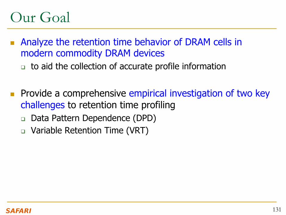
Our Goal n Analyze the retention time behavior of DRAM cells in
modern commodity DRAM devices q to aid the collection of accurate profile information
n Provide a comprehensive empirical investigation of two key challenges to retention time profiling q Data Pattern Dependence (DPD) q Variable Retention Time (VRT)
131

Talk Agenda n DRAM Refresh: Background and Motivation n Challenges and Our Goal n DRAM Characterization Methodology n Foundational Results
q Temperature Dependence q Retention Time Distribution
n Data Pattern Dependence: Analysis and Implications n Variable Retention Time: Analysis and Implications n Conclusions
132

DRAM Testing Platform and Method n Test platform: Developed a DDR3 DRAM testing platform
using the Xilinx ML605 FPGA development board q Temperature controlled
n Tested DRAM chips: 248 commodity DRAM chips from five manufacturers (A,B,C,D,E)
n Seven families based on equal capacity per device: q A 1Gb, A 2Gb q B 2Gb q C 2Gb q D 1Gb, D 2Gb q E 2Gb
133

Experiment Design n Each module tested for multiple rounds of tests.
n Each test searches for the set of cells with a retention time less than a threshold value for a particular data pattern
n High-level structure of a test: q Write data pattern to rows in a DRAM bank q Prevent refresh for a period of time tWAIT, leave DRAM idle q Read stored data pattern, compare to written pattern and
record corrupt cells as those with retention time < tWAIT
n Test details and important issues to pay attention to are discussed in paper
134

Experiment Structure
135
Round 1
Data Pattern XtWAIT = 1.5s
Data Pattern YtWAIT = 1.5s
Data Pattern ZtWAIT = 1.5s
Data Pattern XtWAIT = 1.6s
Data Pattern YtWAIT = 1.6s
Data Pattern ZtWAIT = 1.6s
Data Pattern XtWAIT = 6.0s
Data Pattern YtWAIT = 6.0s
Data Pattern ZtWAIT = 6.0s
Data Pattern XtWAIT = 1.5s
Data Pattern YtWAIT = 1.5s
Data Pattern ZtWAIT = 1.5s
Round 2
Test Round Tests both the data pattern and its complement

Experiment Parameters n Most tests conducted at 45 degrees Celsius
n No cells observed to have a retention time less than 1.5 second at 45oC
n Tested tWAIT in increments of 128ms from 1.5 to 6.1 seconds
136
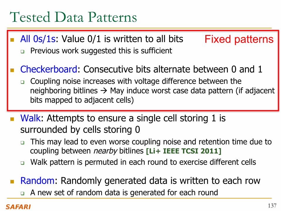
Tested Data Patterns n All 0s/1s: Value 0/1 is written to all bits
q Previous work suggested this is sufficient
n Checkerboard: Consecutive bits alternate between 0 and 1 q Coupling noise increases with voltage difference between the
neighboring bitlines à May induce worst case data pattern (if adjacent bits mapped to adjacent cells)
n Walk: Attempts to ensure a single cell storing 1 is surrounded by cells storing 0 q This may lead to even worse coupling noise and retention time due to
coupling between nearby bitlines [Li+ IEEE TCSI 2011] q Walk pattern is permuted in each round to exercise different cells
n Random: Randomly generated data is written to each row q A new set of random data is generated for each round
137
Fixed patterns

Talk Agenda n DRAM Refresh: Background and Motivation n Challenges and Our Goal n DRAM Characterization Methodology n Foundational Results
q Temperature Dependence q Retention Time Distribution
n Data Pattern Dependence: Analysis and Implications n Variable Retention Time: Analysis and Implications n Conclusions
138

Temperature Stability
139
0 1 2 3 4 5 6 7Time (Hours)
45
50
55
60
65
70
75
Tem
pera
ture
(C)
50C 55C 60C 65C 70C
Tested chips at five different stable temperatures
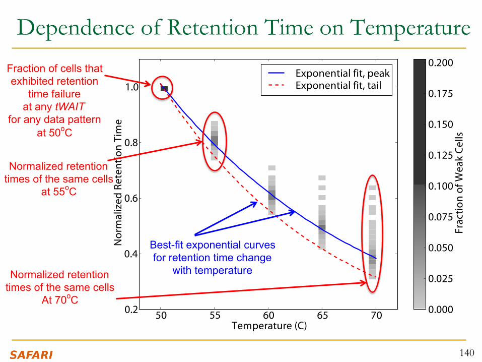
Dependence of Retention Time on Temperature
140
50 55 60 65 70Temperature (C)
0.2
0.4
0.6
0.8
1.0
Nor
mal
ized
Ret
entio
n Ti
me
Exponential fit, peakExponential fit, tail
0.000
0.025
0.050
0.075
0.100
0.125
0.150
0.175
0.200
Frac
tion
of W
eak
Cells
Fraction of cells that exhibited retention
time failure at any tWAIT
for any data pattern at 50oC
Normalized retention times of the same cells
at 55oC
Normalized retention times of the same cells
At 70oC
Best-fit exponential curves for retention time change
with temperature

Dependence of Retention Time on Temperature
141
50 55 60 65 70Temperature (C)
0.2
0.4
0.6
0.8
1.0
Nor
mal
ized
Ret
entio
n Ti
me
Exponential fit, peakExponential fit, tail
0.000
0.025
0.050
0.075
0.100
0.125
0.150
0.175
0.200
Frac
tion
of W
eak
Cells
RelaRonship between retenRon Rme and temperature is consistently bounded (predictable) within a device
Every 10oC temperature increase à 46.5% reducRon in retenRon Rme in the worst case

Retention Time Distribution
142
0 1 2 3 4 5 6 7Retention Time (s)
0.00000
0.00001
0.00002
0.00003
0.00004
0.00005
0.00006
0.00007
0.00008Fr
actio
n of
Cel
ls w
ith R
eten
tion
Tim
e<
X-Ax
is Va
lue
C 2Gb
D 1Gb
D 2Gb
A 2Gb
A 1Gb
E 2Gb
B 2Gb
Minimum tested retenRon Rme ~1.5s at 45C à ~126ms at 85C Very few cells exhibit the lowest retenRon Rmes Shape of the curve consistent with previous works Newer device families have more weak cells than older ones Likely a result of technology scaling
OLDER
NEWER
OLDER
NEWER

Talk Agenda n DRAM Refresh: Background and Motivation n Challenges and Our Goal n DRAM Characterization Methodology n Foundational Results
q Temperature Dependence q Retention Time Distribution
n Data Pattern Dependence: Analysis and Implications n Variable Retention Time: Analysis and Implications n Conclusions
143
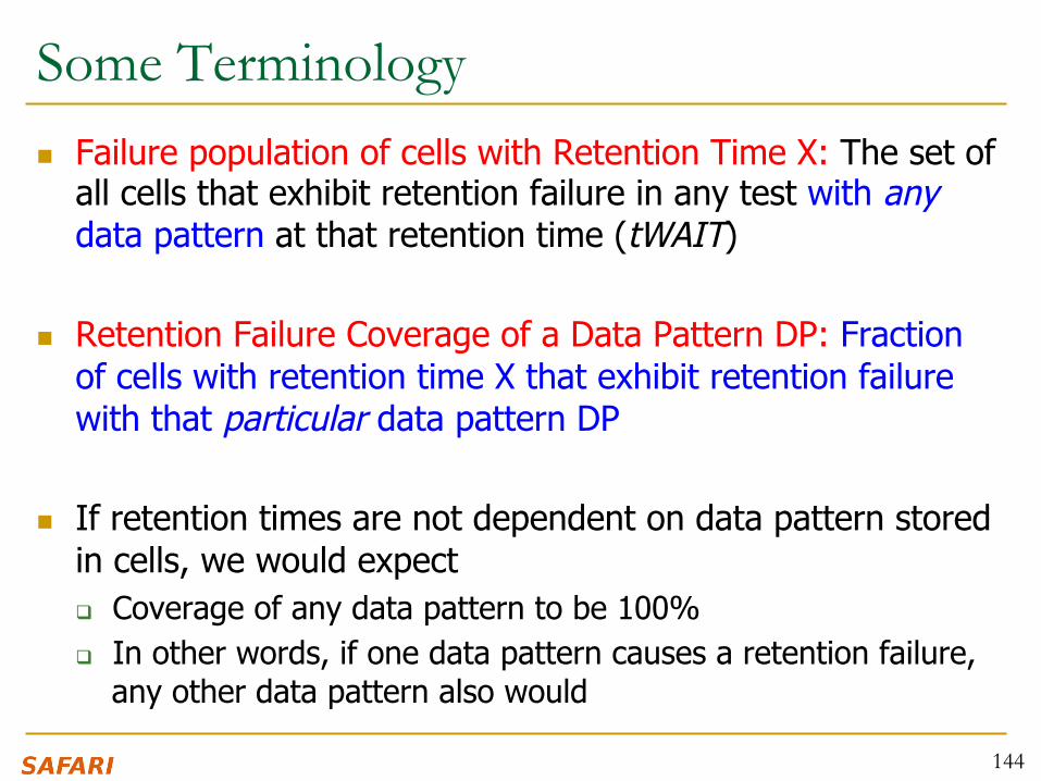
Some Terminology n Failure population of cells with Retention Time X: The set of
all cells that exhibit retention failure in any test with any data pattern at that retention time (tWAIT)
n Retention Failure Coverage of a Data Pattern DP: Fraction of cells with retention time X that exhibit retention failure with that particular data pattern DP
n If retention times are not dependent on data pattern stored in cells, we would expect q Coverage of any data pattern to be 100% q In other words, if one data pattern causes a retention failure,
any other data pattern also would
144

Recall the Tested Data Patterns n All 0s/1s: Value 0/1 is written to all bits
n Checkerboard: Consecutive bits alternate between 0 and 1
n Walk: Attempts to ensure a single cell storing 1 is surrounded by cells storing 0
n Random: Randomly generated data is written to each row
145
Fixed patterns
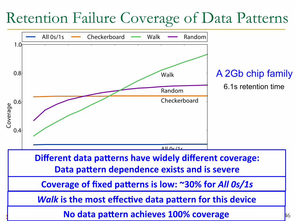
Retention Failure Coverage of Data Patterns
146
0 2 4 6 8 10 12 14 16Number of Rounds
0.0
0.2
0.4
0.6
0.8
1.0
Cove
rage
All 0s/1s
Checkerboard
Random
Walk
All 0s/1s Checkerboard Walk Random
A 2Gb chip family 6.1s retention time
Walk is the most effecRve data pakern for this device Coverage of fixed pakerns is low: ~30% for All 0s/1s
No data pakern achieves 100% coverage
Different data pakerns have widely different coverage: Data pakern dependence exists and is severe

Retention Failure Coverage of Data Patterns
147
0 2 4 6 8 10 12 14 16Number of Rounds
0.0
0.2
0.4
0.6
0.8
1.0
Cove
rage
All 0s/1sCheckerboard
Random
Walk
All 0s/1s Checkerboard Walk Random
B 2Gb chip family 6.1s retention time
Random is the most effecRve data pakern for this device No data pakern achieves 100% coverage
Retention Failure Coverage of Data Patterns
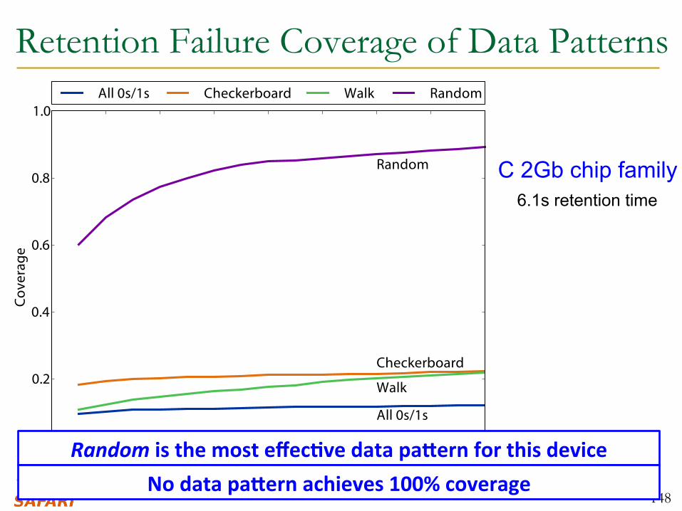
148
0 2 4 6 8 10 12 14 16Number of Rounds
0.0
0.2
0.4
0.6
0.8
1.0
Cove
rage
All 0s/1s
Checkerboard
Random
Walk
All 0s/1s Checkerboard Walk Random
Random is the most effecRve data pakern for this device No data pakern achieves 100% coverage
C 2Gb chip family 6.1s retention time
Data Pattern Dependence: Observations (I) n A cell’s retention time is heavily influenced by data pattern
stored in other cells q Pattern affects the coupling noise, which affects cell leakage
n No tested data pattern exercises the worst case retention time for all cells (no pattern has 100% coverage) q No pattern is able to induce the worst-case coupling noise for
every cell q Problem: Underlying DRAM circuit organization is not known to
the memory controller à very hard to construct a pattern that exercises the worst-case cell leakage à Opaque mapping of addresses to physical DRAM geometry à Internal remapping of addresses within DRAM to tolerate faults à Second order coupling effects are very hard to determine
149
Data Pattern Dependence: Observations (II) n Fixed, simple data patterns have low coverage
q They do not exercise the worst-case coupling noise
n The effectiveness of each data pattern varies significantly between DRAM devices (of the same or different vendors) q Underlying DRAM circuit organization likely differs between
different devices à patterns leading to worst coupling are different in different devices
n Technology scaling appears to increase the impact of data pattern dependence q Scaling reduces the physical distance between circuit elements,
increasing the magnitude of coupling effects
150

Effect of Technology Scaling on DPD
151
0 2 4 6 8 10 12 14 16Number of Rounds
0.0
0.2
0.4
0.6
0.8
1.0
Cove
rage
All 0s/1s
Checkerboard
Walk
All 0s/1s Checkerboard Walk
0 2 4 6 8 10 12 14 16Number of Rounds
0.0
0.2
0.4
0.6
0.8
1.0
Cove
rage
All 0s/1s
Checkerboard
Random
Walk
All 0s/1s Checkerboard Walk Random
A 1Gb chip family A 2Gb chip family
The lowest-‐coverage data pakern achieves much lower coverage for the smaller technology node

DPD: Implications on Profiling Mechanisms n Any retention time profiling mechanism must handle data pattern
dependence of retention time n Intuitive approach: Identify the data pattern that induces the
worst-case retention time for a particular cell or device
n Problem 1: Very hard to know at the memory controller which bits actually interfere with each other due to q Opaque mapping of addresses to physical DRAM geometry à
logically consecutive bits may not be physically consecutive q Remapping of faulty bitlines/wordlines to redundant ones internally
within DRAM
n Problem 2: Worst-case coupling noise is affected by non-obvious second order bitline coupling effects
152

DPD: Suggestions (for Future Work) n A mechanism for identifying worst-case data pattern(s)
likely requires support from DRAM device q DRAM manufacturers might be in a better position to do this q But, the ability of the manufacturer to identify and expose the
entire retention time profile is limited due to VRT
n An alternative approach: Use random data patterns to increase coverage as much as possible; handle incorrect retention time estimates with ECC q Need to keep profiling time in check q Need to keep ECC overhead in check
153
Talk Agenda n DRAM Refresh: Background and Motivation n Challenges and Our Goal n DRAM Characterization Methodology n Foundational Results
q Temperature Dependence q Retention Time Distribution
n Data Pattern Dependence: Analysis and Implications n Variable Retention Time: Analysis and Implications n Conclusions
154

Variable Retention Time n Retention time of a cell can vary over time
n A cell can randomly switch between multiple leakage current states due to Trap-Assisted Gate-Induced Drain Leakage, which appears to be a random process
[Yaney+ IEDM 1987, Restle+ IEDM 1992]
155
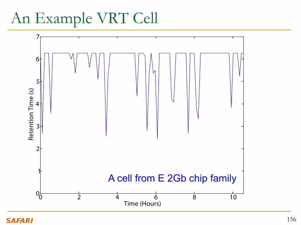
An Example VRT Cell
156
0 2 4 6 8 10Time (Hours)
0
1
2
3
4
5
6
7Re
tent
ion
Tim
e (s
)
A cell from E 2Gb chip family

VRT: Questions and Methodology n Key Questions
q How prevalent is VRT in modern DRAM devices? q What is the timescale of observation of the lowest retention
time state? q What are the implications on retention time profiling?
n Test Methodology q Each device was tested for at least 1024 rounds over 24 hours q Temperature fixed at 45oC q Data pattern used is the most effective data pattern for each
device q For each cell that fails at any retention time, we record the
minimum and the maximum retention time observed
157

Variable Retention Time
158
0 1 2 3 4 5 6 7Minimum Retention Time (s)
0
1
2
3
4
5
6
7M
axim
um R
eten
tion
Tim
e (s
)
6.0
5.4
4.8
4.2
3.6
3.0
2.4
1.8
1.2
0.6
0.0
log1
0(Fr
actio
n of
Cel
ls)
A 2Gb chip family
Min ret time = Max ret time Expected if no VRT
Most failing cells exhibit VRT
Many failing cells jump from very high retention time to very low
Variable Retention Time
159
0 1 2 3 4 5 6 7Minimum Retention Time (s)
0
1
2
3
4
5
6
7M
axim
um R
eten
tion
Tim
e (s
)
6.0
5.4
4.8
4.2
3.6
3.0
2.4
1.8
1.2
0.6
0.0
log1
0(Fr
actio
n of
Cel
ls)
B 2Gb chip family

Variable Retention Time
160
0 1 2 3 4 5 6 7Minimum Retention Time (s)
0
1
2
3
4
5
6
7M
axim
um R
eten
tion
Tim
e (s
)
6.0
5.4
4.8
4.2
3.6
3.0
2.4
1.8
1.2
0.6
0.0
log1
0(Fr
actio
n of
Cel
ls)
C 2Gb chip family
VRT: Observations So Far n VRT is common among weak cells (i.e., those cells that
experience low retention times)
n VRT can result in significant retention time changes q Difference between minimum and maximum retention times of
a cell can be more than 4x, and may not be bounded q Implication: Finding a retention time for a cell and using a
guardband to ensure minimum retention time is “covered” requires a large guardband or may not work
n Retention time profiling mechanisms must identify lowest retention time in the presence of VRT q Question: How long to profile a cell to find its lowest retention
time state? 161

Time Between Retention Time State Changes
n How much time does a cell spend in a high retention state before switching to the minimum observed retention time state?
162
Time Spent in High Retention Time State
163
0 20000 40000 60000 80000Time Spent in High Retention Time State (s)
Rela
tive
Freq
uenc
y
A 2Gb chip family
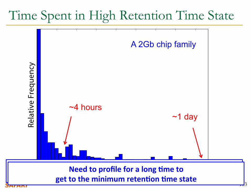
~4 hours ~1 day
Time scale at which a cell switches to the low retenRon Rme state can be very long (~ 1 day or longer) Need to profile for a long Rme to
get to the minimum retenRon Rme state

Time Spent in High Retention Time State
164
0 20000 40000 60000 80000Time Spent in High Retention Time State (s)
Rela
tive
Freq
uenc
y
B 2Gb chip family

Time Spent in High Retention Time State
165
0 20000 40000 60000 80000Time Spent in High Retention Time State (s)
Rela
tive
Freq
uenc
y
C 2Gb chip family

VRT: Implications on Profiling Mechanisms n Problem 1: There does not seem to be a way of
determining if a cell exhibits VRT without actually observing a cell exhibiting VRT q VRT is a memoryless random process [Kim+ JJAP 2010]
n Problem 2: VRT complicates retention time profiling by DRAM manufacturers q Exposure to very high temperatures can induce VRT in cells that
were not previously susceptible à can happen during soldering of DRAM chips à manufacturer’s retention time profile may not be accurate
n One option for future work: Use ECC to continuously profile DRAM online while aggressively reducing refresh rate q Need to keep ECC overhead in check
166

Talk Agenda n DRAM Refresh: Background and Motivation n Challenges and Our Goal n DRAM Characterization Methodology n Foundational Results
q Temperature Dependence q Retention Time Distribution
n Data Pattern Dependence: Analysis and Implications n Variable Retention Time: Analysis and Implications n Conclusions
167

Summary and Conclusions n DRAM refresh is a critical challenge in scaling DRAM technology
efficiently to higher capacities and smaller feature sizes n Understanding the retention time of modern DRAM devices can
enable old or new methods to reduce the impact of refresh q Many mechanisms require accurate and reliable retention time profiles
n We presented the first work that comprehensively examines data retention behavior in modern commodity DRAM devices q Characterized 248 devices from five manufacturers
n Key findings: Retention time of a cell significantly depends on data pattern stored in other cells (data pattern dependence) and changes over time via a random process (variable retention time) q Discussed the underlying reasons and provided suggestions
n Future research on retention time profiling should solve the challenges posed by the DPD and VRT phenomena
168

1 Carnegie Mellon University 2 Intel Corporation
Jamie Liu1 Ben Jaiyen1 Yoongu Kim1 Chris Wilkerson2 Onur Mutlu1
An Experimental Study of Data Retention Behavior
in Modern DRAM Devices
Implications for Retention Time Profiling Mechanisms

Enabling Emerging Memory Technologies
170
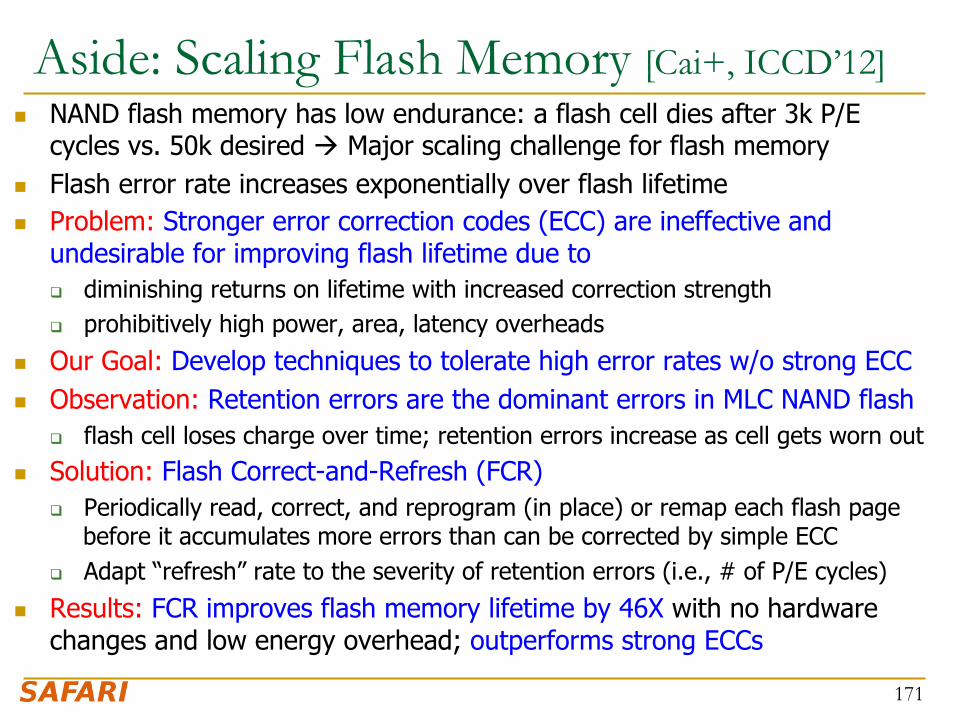
Aside: Scaling Flash Memory [Cai+, ICCD’12]
171
n NAND flash memory has low endurance: a flash cell dies after 3k P/E cycles vs. 50k desired à Major scaling challenge for flash memory
n Flash error rate increases exponentially over flash lifetime n Problem: Stronger error correction codes (ECC) are ineffective and
undesirable for improving flash lifetime due to q diminishing returns on lifetime with increased correction strength q prohibitively high power, area, latency overheads
n Our Goal: Develop techniques to tolerate high error rates w/o strong ECC n Observation: Retention errors are the dominant errors in MLC NAND flash
q flash cell loses charge over time; retention errors increase as cell gets worn out n Solution: Flash Correct-and-Refresh (FCR)
q Periodically read, correct, and reprogram (in place) or remap each flash page before it accumulates more errors than can be corrected by simple ECC
q Adapt “refresh” rate to the severity of retention errors (i.e., # of P/E cycles)
n Results: FCR improves flash memory lifetime by 46X with no hardware changes and low energy overhead; outperforms strong ECCs
Solution 2: Emerging Memory Technologies n Some emerging resistive memory technologies seem more
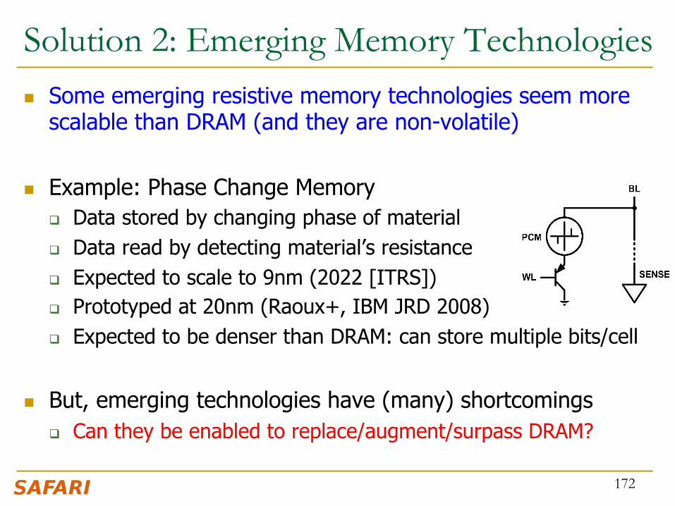
scalable than DRAM (and they are non-volatile)
n Example: Phase Change Memory q Data stored by changing phase of material q Data read by detecting material’s resistance q Expected to scale to 9nm (2022 [ITRS]) q Prototyped at 20nm (Raoux+, IBM JRD 2008) q Expected to be denser than DRAM: can store multiple bits/cell
n But, emerging technologies have (many) shortcomings q Can they be enabled to replace/augment/surpass DRAM?
172
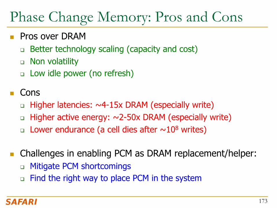
Phase Change Memory: Pros and Cons n Pros over DRAM
q Better technology scaling (capacity and cost) q Non volatility q Low idle power (no refresh)
n Cons q Higher latencies: ~4-15x DRAM (especially write) q Higher active energy: ~2-50x DRAM (especially write) q Lower endurance (a cell dies after ~108 writes)
n Challenges in enabling PCM as DRAM replacement/helper: q Mitigate PCM shortcomings q Find the right way to place PCM in the system
173
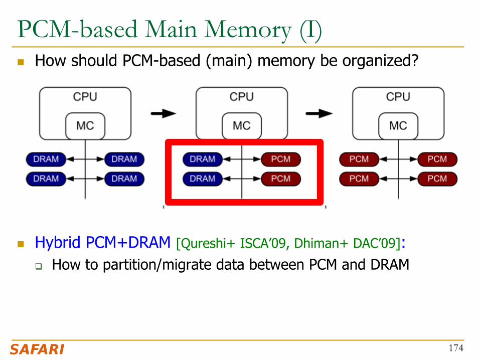
PCM-based Main Memory (I) n How should PCM-based (main) memory be organized?
n Hybrid PCM+DRAM [Qureshi+ ISCA’09, Dhiman+ DAC’09]: q How to partition/migrate data between PCM and DRAM
174

PCM-based Main Memory (II) n How should PCM-based (main) memory be organized?
n Pure PCM main memory [Lee et al., ISCA’09, Top Picks’10]:
q How to redesign entire hierarchy (and cores) to overcome PCM shortcomings
175

PCM-Based Memory Systems: Research Challenges
n Partitioning q Should DRAM be a cache or main memory, or configurable? q What fraction? How many controllers?
n Data allocation/movement (energy, performance, lifetime) q Who manages allocation/movement? q What are good control algorithms? q How do we prevent degradation of service due to wearout?
n Design of cache hierarchy, memory controllers, OS q Mitigate PCM shortcomings, exploit PCM advantages
n Design of PCM/DRAM chips and modules q Rethink the design of PCM/DRAM with new requirements
176
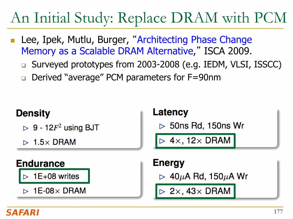
An Initial Study: Replace DRAM with PCM n Lee, Ipek, Mutlu, Burger, “Architecting Phase Change
Memory as a Scalable DRAM Alternative,” ISCA 2009. q Surveyed prototypes from 2003-2008 (e.g. IEDM, VLSI, ISSCC) q Derived “average” PCM parameters for F=90nm
177

Results: Naïve Replacement of DRAM with PCM n Replace DRAM with PCM in a 4-core, 4MB L2 system n PCM organized the same as DRAM: row buffers, banks, peripherals n 1.6x delay, 2.2x energy, 500-hour average lifetime
n Lee, Ipek, Mutlu, Burger, “Architecting Phase Change Memory as a
Scalable DRAM Alternative,” ISCA 2009. 178
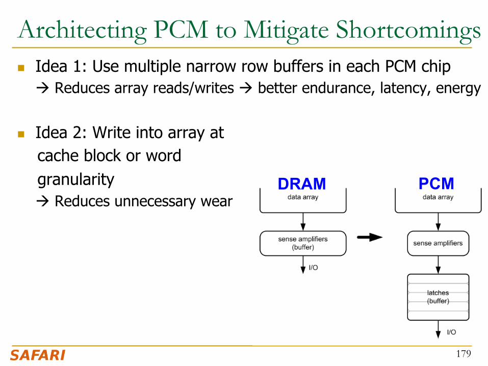
Architecting PCM to Mitigate Shortcomings n Idea 1: Use multiple narrow row buffers in each PCM chip
à Reduces array reads/writes à better endurance, latency, energy
n Idea 2: Write into array at cache block or word granularity
à Reduces unnecessary wear
179
DRAM PCM
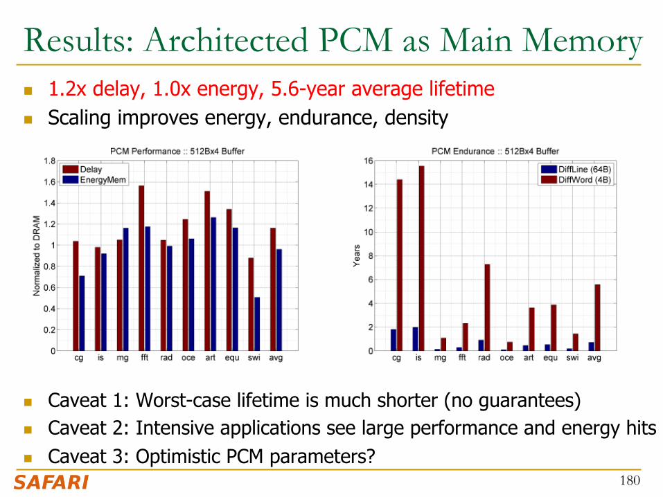
Results: Architected PCM as Main Memory n 1.2x delay, 1.0x energy, 5.6-year average lifetime n Scaling improves energy, endurance, density
n Caveat 1: Worst-case lifetime is much shorter (no guarantees) n Caveat 2: Intensive applications see large performance and energy hits n Caveat 3: Optimistic PCM parameters?
180

Hybrid Memory Systems
Meza, Chang, Yoon, Mutlu, Ranganathan, “Enabling Efficient and Scalable Hybrid Memories,” IEEE Comp. Arch. Letters, 2012.
CPU DRAMCtrl
Fast, durable Small,
leaky, volatile, high-cost
Large, non-volatile, low-cost Slow, wears out, high active energy
PCM Ctrl DRAM Phase Change Memory (or Tech. X)
Hardware/software manage data allocation and movement to achieve the best of multiple technologies
(5-9 years of average lifetime)

One Option: DRAM as a Cache for PCM n PCM is main memory; DRAM caches memory rows/blocks
q Benefits: Reduced latency on DRAM cache hit; write filtering
n Memory controller hardware manages the DRAM cache q Benefit: Eliminates system software overhead
n Three issues: q What data should be placed in DRAM versus kept in PCM? q What is the granularity of data movement? q How to design a low-cost hardware-managed DRAM cache?
n Two idea directions: q Locality-aware data placement [Yoon+ , ICCD 2012]
q Cheap tag stores and dynamic granularity [Meza+, IEEE CAL 2012]
182

DRAM vs. PCM: An Observation n Row buffers are the same in DRAM and PCM n Row buffer hit latency same in DRAM and PCM n Row buffer miss latency small in DRAM, large in PCM
n Accessing the row buffer in PCM is fast n What incurs high latency is the PCM array access à avoid this
183
CPU DRAMCtrl
PCM Ctrl
Bank Bank Bank Bank
Row buffer DRAM Cache PCM Main Memory
N ns row hit Fast row miss
N ns row hit Slow row miss

Row-Locality-Aware Data Placement n Idea: Cache in DRAM only those rows that
q Frequently cause row buffer conflicts à because row-conflict latency is smaller in DRAM
q Are reused many times à to reduce cache pollution and bandwidth waste
n Simplified rule of thumb: q Streaming accesses: Better to place in PCM q Other accesses (with some reuse): Better to place in DRAM
n Bridges half of the performance gap between all-DRAM and all-PCM memory on memory-intensive workloads
n Yoon et al., “Row Buffer Locality-Aware Caching Policies for Hybrid Memories,” ICCD 2012.
184
Row-Locality-Aware Data Placement: Mechanism
n For a subset of rows in PCM, memory controller: q Tracks row conflicts as a predictor of future locality q Tracks accesses as a predictor of future reuse
n Cache a row in DRAM if its row conflict and access counts are greater than certain thresholds
n Determine thresholds dynamically to adjust to application/workload characteristics q Simple cost/benefit analysis every fixed interval
185
Implementation: “Statistics Store” • Goal: To keep count of row buffer misses to recently used rows in PCM
• Hardware structure in memory controller – OperaOon is similar to a cache
• Input: row address • Output: row buffer miss count
– 128-‐set 16-‐way staOsOcs store (9.25KB) achieves system performance within 0.3% of an unlimited-‐sized staOsOcs store
186

Evaluation Methodology • Cycle-‐level x86 CPU-‐memory simulator
– CPU: 16 out-‐of-‐order cores, 32KB private L1 per core, 512KB shared L2 per core
– Memory: 1GB DRAM (8 banks), 16GB PCM (8 banks), 4KB migraOon granularity
• 36 mulO-‐programmed server, cloud workloads – Server: TPC-‐C (OLTP), TPC-‐H (Decision Support) – Cloud: Apache (Webserv.), H.264 (Video), TPC-‐C/H
• Metrics: Weighted speedup (perf.), perf./Waq (energy eff.), Maximum slowdown (fairness)
187

Comparison Points • ConvenRonal LRU Caching • FREQ: Access-‐frequency-‐based caching
– Places “hot data” in cache [Jiang+ HPCA’10] – Cache to DRAM rows with accesses ≥ threshold – Row buffer locality-‐unaware
• FREQ-‐Dyn: AdapOve Freq.-‐based caching – FREQ + our dynamic threshold adjustment – Row buffer locality-‐unaware
• RBLA: Row buffer locality-‐aware caching • RBLA-‐Dyn: AdapOve RBL-‐aware caching 188
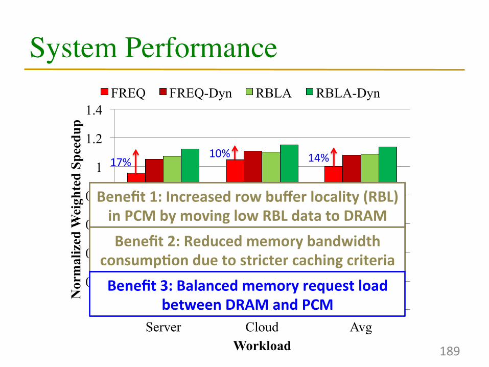
0
0.2
0.4
0.6
0.8
1
1.2
1.4
Server Cloud Avg
Nor
mal
ized
Wei
ghte
d Sp
eedu
p
Workload
FREQ FREQ-Dyn RBLA RBLA-Dyn
10%
System Performance
189
14%
Benefit 1: Increased row buffer locality (RBL) in PCM by moving low RBL data to DRAM
17%
Benefit 1: Increased row buffer locality (RBL) in PCM by moving low RBL data to DRAM Benefit 2: Reduced memory bandwidth
consumpRon due to stricter caching criteria Benefit 2: Reduced memory bandwidth
consumpRon due to stricter caching criteria Benefit 3: Balanced memory request load
between DRAM and PCM

0
0.2
0.4
0.6
0.8
1
1.2
Server Cloud Avg
Nor
mal
ized
Avg
Mem
ory
Lat
ency
Workload
FREQ FREQ-Dyn RBLA RBLA-Dyn
Average Memory Latency
190
14%
9% 12%

0
0.2
0.4
0.6
0.8
1
1.2
Server Cloud Avg
Nor
mal
ized
Per
f. pe
r Wat
t
Workload
FREQ FREQ-Dyn RBLA RBLA-Dyn
Memory Energy Efficiency
191
Increased performance & reduced data movement between DRAM and PCM
7% 10% 13%
0
0.2
0.4
0.6
0.8
1
1.2
Server Cloud Avg
Nor
mal
ized
Max
imum
Slo
wdo
wn
Workload
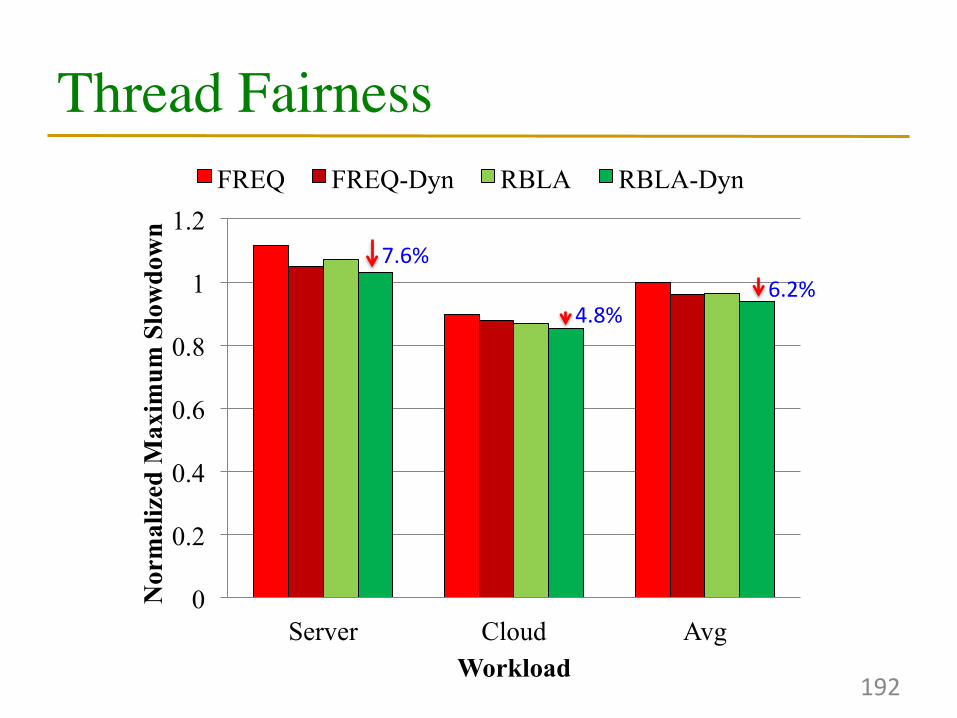
FREQ FREQ-Dyn RBLA RBLA-Dyn
Thread Fairness
192
7.6%
4.8% 6.2%

0 0.2 0.4 0.6 0.8
1 1.2 1.4 1.6 1.8
2
Weighted Speedup Max. Slowdown Perf. per Watt Normalized Metric
16GB PCM RBLA-Dyn 16GB DRAM
0 0.2 0.4 0.6 0.8
1 1.2 1.4 1.6 1.8
2
Nor
mal
ized
Wei
ghte
d Sp
eedu
p
0
0.2
0.4
0.6
0.8
1
1.2
Nor
mal
ized
Max
. Slo
wdo
wn
Compared to All-PCM/DRAM
193
Our mechanism achieves 31% beker performance than all PCM, within 29% of all DRAM
performance
31%
29%
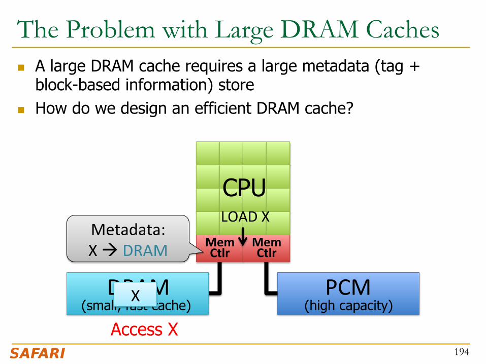
The Problem with Large DRAM Caches n A large DRAM cache requires a large metadata (tag +
block-based information) store n How do we design an efficient DRAM cache?
194
DRAM PCM
CPU
(small, fast cache) (high capacity)
Mem Ctlr
Mem Ctlr
LOAD X
Access X
Metadata: X à DRAM
X

Idea 1: Tags in Memory n Store tags in the same row as data in DRAM
q Store metadata in same row as their data q Data and metadata can be accessed together
n Benefit: No on-chip tag storage overhead n Downsides:
q Cache hit determined only after a DRAM access q Cache hit requires two DRAM accesses
195
Cache block 2 Cache block 0 Cache block 1 DRAM row
Tag0 Tag1 Tag2
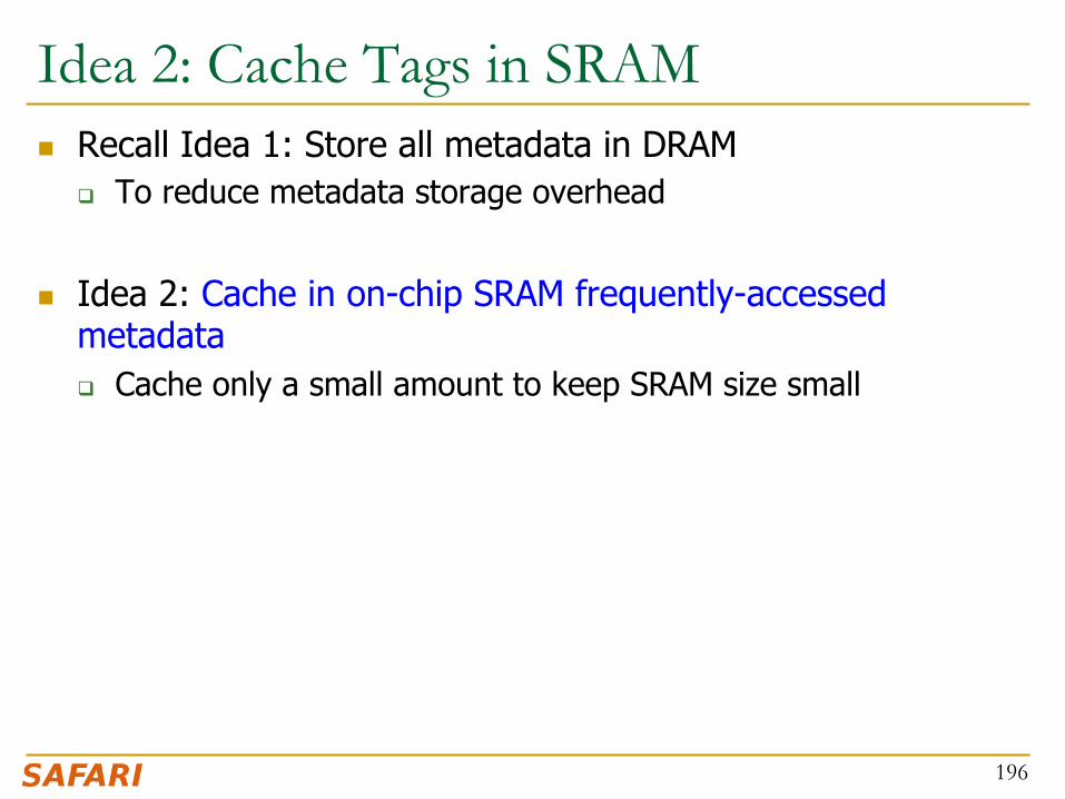
Idea 2: Cache Tags in SRAM n Recall Idea 1: Store all metadata in DRAM
q To reduce metadata storage overhead
n Idea 2: Cache in on-chip SRAM frequently-accessed metadata q Cache only a small amount to keep SRAM size small
196

Idea 3: Dynamic Data Transfer Granularity n Some applications benefit from caching more data
q They have good spatial locality
n Others do not q Large granularity wastes bandwidth and reduces cache
utilization
n Idea 3: Simple dynamic caching granularity policy q Cost-benefit analysis to determine best DRAM cache block size q Group main memory into sets of rows q Some row sets follow a fixed caching granularity q The rest of main memory follows the best granularity
n Cost–benefit analysis: access latency versus number of cachings n Performed every quantum
197

TIMBER Tag Management n A Tag-In-Memory BuffER (TIMBER)
q Stores recently-used tags in a small amount of SRAM
n Benefits: If tag is cached:
q no need to access DRAM twice q cache hit determined quickly
198
Tag0 Tag1 Tag2 Row0
Tag0 Tag1 Tag2 Row27
Row Tag
LOAD X
Cache block 2 Cache block 0 Cache block 1 DRAM row
Tag0 Tag1 Tag2
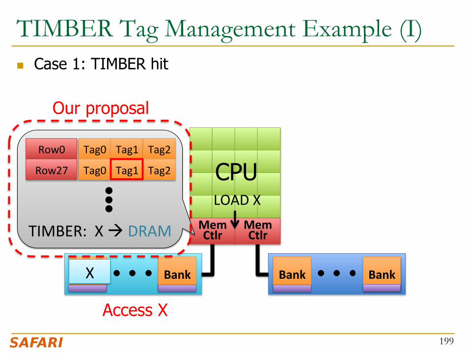
TIMBER Tag Management Example (I) n Case 1: TIMBER hit
199
Bank Bank Bank Bank
CPU
Mem Ctlr
Mem Ctlr
LOAD X
TIMBER: X à DRAM
X
Access X
Tag0 Tag1 Tag2 Row0
Tag0 Tag1 Tag2 Row27
Our proposal

TIMBER Tag Management Example (II) n Case 2: TIMBER miss
200
CPU
Mem Ctlr
Mem Ctlr
LOAD Y
Y à DRAM
Bank Bank Bank Bank
Access Metadata(Y)
Y
1. Access M(Y)
Tag0 Tag1 Tag2 Row0
Tag0 Tag1 Tag2 Row27
Miss
M(Y)
2. Cache M(Y)
Row143
3. Access Y (row hit)

Methodology n System: 8 out-of-order cores at 4 GHz
n Memory: 512 MB direct-mapped DRAM, 8 GB PCM q 128B caching granularity q DRAM row hit (miss): 200 cycles (400 cycles) q PCM row hit (clean / dirty miss): 200 cycles (640 / 1840 cycles)
n Evaluated metadata storage techniques q All SRAM system (8MB of SRAM) q Region metadata storage q TIM metadata storage (same row as data) q TIMBER, 64-entry direct-mapped (8KB of SRAM)
201

0
0.1
0.2
0.3
0.4
0.5
0.6
0.7
0.8
0.9
1
SRAM Region TIM TIMBER TIMBER-‐Dyn
Normalized
Weighted Speedu
p
202
TIMBER Performance
-‐6%
Meza, Chang, Yoon, Mutlu, Ranganathan, “Enabling Efficient and Scalable Hybrid Memories,” IEEE Comp. Arch. Leqers, 2012.

0
0.2
0.4
0.6
0.8
1
1.2
SRAM Region TIM TIMBER TIMBER-‐Dyn
Normalized
Perform
ance per W
ak
(for M
emory System
)
203
TIMBER Energy Efficiency 18%
Meza, Chang, Yoon, Mutlu, Ranganathan, “Enabling Efficient and Scalable Hybrid Memories,” IEEE Comp. Arch. Leqers, 2012.
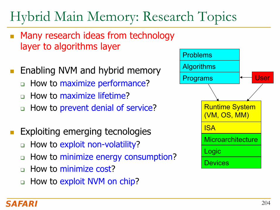
Hybrid Main Memory: Research Topics n Many research ideas from technology
layer to algorithms layer
n Enabling NVM and hybrid memory q How to maximize performance? q How to maximize lifetime? q How to prevent denial of service?
n Exploiting emerging tecnologies q How to exploit non-volatility? q How to minimize energy consumption? q How to minimize cost? q How to exploit NVM on chip?
204
Microarchitecture
ISA
Programs
Algorithms Problems
Logic
Devices
Runtime System (VM, OS, MM)
User

Security Challenges of Emerging Technologies
1. Limited endurance à Wearout attacks 2. Non-volatility à Data persists in memory after powerdown à Easy retrieval of privileged or private information 3. Multiple bits per cell à Information leakage (via side channel)
205
Securing Emerging Memory Technologies
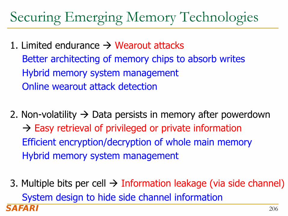
1. Limited endurance à Wearout attacks Better architecting of memory chips to absorb writes Hybrid memory system management Online wearout attack detection 2. Non-volatility à Data persists in memory after powerdown à Easy retrieval of privileged or private information Efficient encryption/decryption of whole main memory Hybrid memory system management 3. Multiple bits per cell à Information leakage (via side channel) System design to hide side channel information
206