56-pin ck505 for intel desktop systems ics9lp525-2 filepci_f5/itp_en 7 50 gndref gndpci 8 49...
TRANSCRIPT

ICS9LP525-2
IDT® PC MAIN CLOCK 1397—11/08/10
56-pin CK505 for Intel Desktop Systems
1
DATASHEET
Pin Configuration
Recommended Application:
CK505 clock, 56-pin Intel Yellow Cover part
Output Features:
• 2 - CPU differential low power push-pull pairs
• 7- SRC differential low power push-pull pairs
• 1 - CPU/SRC selectable differential low power push-pull pair
• 1 - SRC/DOT selectable differential low power push-pull pair
• 5 - PCI, 33MHz
• 1 - PCI_F, 33MHz free running
• 1 - USB, 48MHz
• 1 - REF, 14.318MHz
Key Specifications:
• CPU outputs cycle-cycle jitter < 85ps
• SRC output cycle-cycle jitter < 125ps
• PCI outputs cycle-cycle jitter < 250ps
• +/- 100ppm frequency accuracy on all outputs
• SRC are PCIe Gen2 compliant
PCI0/CR#_A 1 56 SCLK
VDDPCI 2 55 SDATA
PCI1/CR#_B 3 54 REF0/FSLC/TEST_SEL
PCI2/TME 4 53 VDDREF
PCI3/CFG0 5 52 X1
PCI4/SRC5_EN 6 51 X2
PCI_F5/ITP_EN 7 50 GNDREF
GNDPCI 8 49 FSLB/TEST_MODE
VDD48 9 48 CK_PWRGD/PD#
USB_48MHz/FSLA 10 47 VDDCPU
GND48 11 46 CPUT0
VDD96_IO 12 45 CPUC0
DOTT_96/SRCT0 13 44 GNDCPU
DOTC_96/SRCC0 14 43 CPUT1_F
GND 15 42 CPUC1_F
VDD 16 41 VDDCPU_IO
SRCT1/SE1 17 40 VOUT
SRCC1/SE2 18 39 CPUT2_ITP/SRCT8
GND 19 38 CPUC2_ITP/SRCC8
VDDPLL3_IO 20 37 VDDSRC_IO
SRCT2/SATAT 21 36 SRCT7/CR#_F
SRCC2/SATAC 22 35 SRCC7/CR#_E
GNDSRC 23 34 GNDSRC
SRCT3/CR#_C 24 33 SRCT6
SRCC3/CR#_D 25 32 SRCC6
VDDSRC_IO 26 31 VDDSRC
SRCT4 27 30 PCI_STOP#/SRCT5SRCC4 28 29 CPU_STOP#/SRCC5
56-SSOP & TSSOP
9L
P5
25
-2
Features/Benefits:
• Supports spread spectrum modulation, default is 0.5%
down spread
• Uses external 14.318MHz crystal, external crystal load
caps are required for frequency tuning
• Selectable SRC differential push-pull pair/two singleended outputs
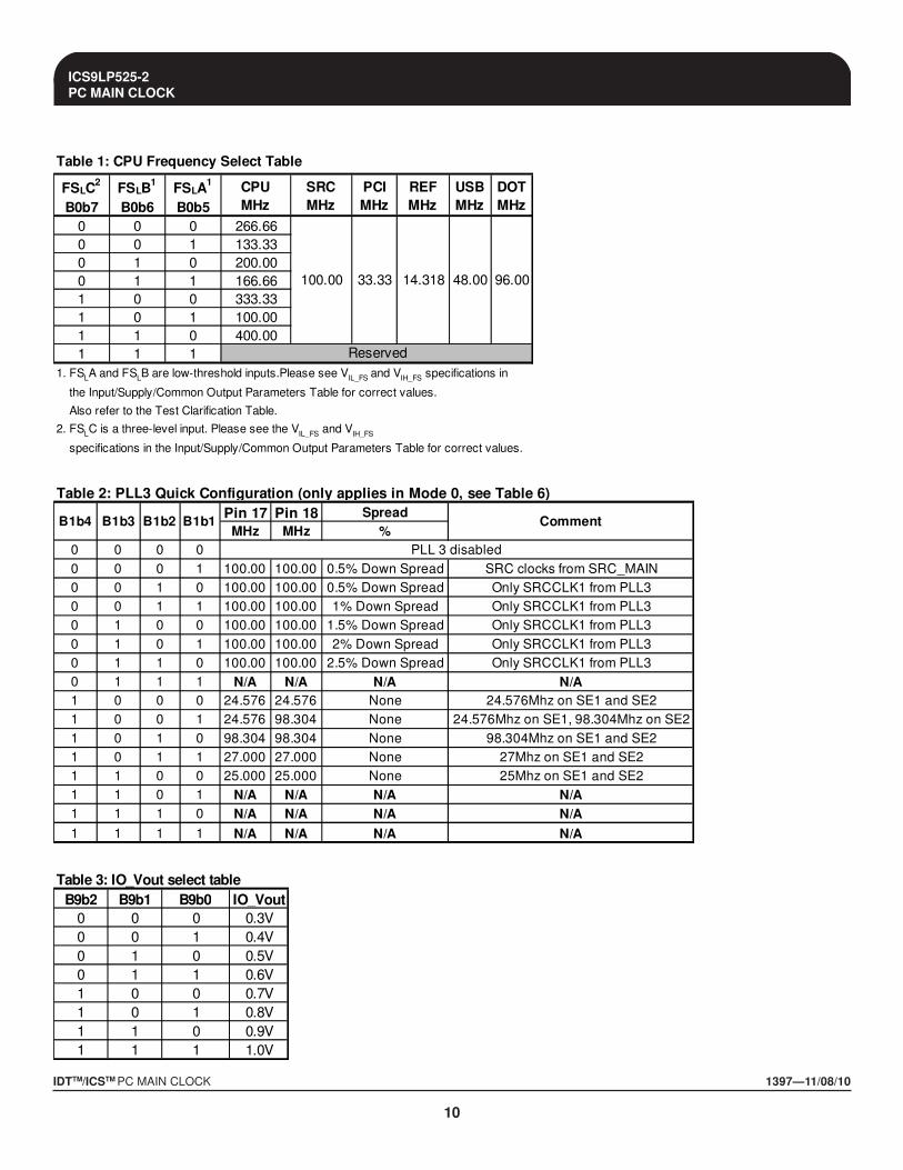
Table 1: CPU Frequency Select Table
FSLC2
B0b7
FSLB1
B0b6
FSLA1
B0b5
CPU
MHz
SRC
MHz
PCI
MHz
REF
MHz
USB
MHz
DOT
MHz
0 0 0 266.66
0 0 1 133.33
0 1 0 200.00
0 1 1 166.66
1 0 0 333.33
1 0 1 100.00
1 1 0 400.00
1 1 1
1. FSLA and FSLB are low-threshold inputs.Please see VIL_FS and VIH_FS specifications in
the Input/Supply/Common Output Parameters Table for correct values.
Also refer to the Test Clarification Table.
2. FSLC is a three-level input. Please see the VIL_FS and VIH_FS
specifications in the Input/Supply/Common Output Parameters Table for correct values.
Reserved
100.00 33.33 14.318 48.00 96.00

IDTTM/ICSTM PC MAIN CLOCK 1397—11/08/10
ICS9LP525-2PC MAIN CLOCK
2
Pin DescriptionPIN # PIN NAME TYPE DESCRIPTION
1 PCI0/CR#_A I/O
3.3V PCI clock output or Clock Request control A for either SRC0 or SRC2 pair
The power-up default is PCI0 output, but this pin may also be used as a Clock Request control of SRC pair 0 or SRC pair 2 via
SMBus. Before configuring this pin as a Clock Request Pin, the PCI output must first be disabled in byte 2, bit 0 of SMBus address
space . After the PCI output is disabled (high-Z), the pin can then be set to serve as a Clock Request pin for either SRC pair 2 or
pair 0 using the CRA#_EN bit located in byte 5 of SMBUs address space.
Byte 5, bit 7
0 = PCI0 enabled (default)
1= CRA# enabled. Byte 5, bit 6 controls whether CRA# controls SRC0 or SRC2 pair
Byte 5, bit 6
0 = CRA# controls SRC0 pair (default),
1= CRA# controls SRC2 pair
2 VDDPCI PWR Power supply for PCI clocks, nominal 3.3V
3 PCI1/CR#_B I/O
3.3V PCI clock output/Clock Request control B for either SRC1 or SRC4 pair
The power-up default is PCI1 output, but this pin may also be used as a Clock Request control of SRC pair 1 or SRC pair 4 via
SMBus. Before configuring this pin as a Clock Request Pin, the PCI output must first be disabled in byte 2, bit 1 of SMBus address
space . After the PCI output is disabled (high-Z), the pin can then be set to serve as a Clock Request pin for either SRC pair 1 or
pair 4 using the CRB#_EN bit located in byte 5 of SMBUs address space.
Byte 5, bit 5
0 = PCI1 enabled (default)
1= CRB# enabled. Byte 5, bit 6 controls whether CRB# controls SRC1 or SRC4 pair
Byte 5, bit 4
0 = CRB# controls SRC1 pair (default)
1= CRB# controls SRC4 pair
4 PCI2/TME I/O
3.3V PCI clock output / Trusted Mode Enable(TME) Latched Input. This pin is sampled on power-up as follows
0=Overclocking of CPU and SRC allowed
1=Overclocking of CPU and SRC NOT allowed
After being sampled on power-up, this pin becomes a 3.3V PCI Output
5 PCI3/CFG0 I/O 3.3V PCI clock output/Configuration Strap. See PCI3 Configuration Table for more information
6 PCI4/SRC5_EN I/O
3.3V PCI clock output / SRC5 pair or PCI_STOP#/CPU_STOP# enable strap. On powerup, the logic value on this pin determines if
the SRC5 pair is enabled or if CPU_STOP#/PCI_STOP# is enabled (pins 29 and 30). The latched value controls the pin function on
pins 29 and 30 as follows
0 = PCI_STOP#/CPU_STOP#
1 = SRC5/SRC5#
7 PCI_F5/ITP_EN I/O
Free running PCI clock output and ITP/SRC8 enable strap. This output is not affected by the state of the PCI_STOP# pin. On
powerup, the state of this pin determines whether pins 38 and 39 are an ITP or SRC pair.
0 =SRC8/SRC8#
1 = ITP/ITP#
8 GNDPCI PWR Ground pin for the PCI outputs
9 VDD48 PWR Power pin for the 48MHz output and PLL.3.3V
10 USB_48MHz/FSLA I/O3.3V tolerant input for CPU frequency selection. Refer to input electrical characteristics for Vil_FS and Vih_FS values. / Fixed
48MHz USB clock output. 3.3V.
11 GND48 PWR Ground pin for the 48MHz outputs
12 VDD96_IO PWR Power supply for DOT96 clocks, nominal 0.8V from source/emitter of external pass transistor.
13 DOTT_96/SRCT0 OUT
True clock of low power differential SRC or DOT96. The power-up default function is SRC0. After powerup, this pin function may be
changed to DOT96 via SMBus Byte 1, bit 7 as follows:
0= SRC0
1=DOT96
14 DOTC_96/SRCC0 OUT
Complement clock of low power differential SRC or DOT96. The power-up default function is SRC0#. After powerup, this pin
function may be changed to DOT96# via SMBus Byte 1, bit 7 as follows
0= SRC0#
1=DOT96#
15 GND PWR Ground pin.
16 VDD PWR Power supply, nominal 3.3V
17 SRCT1/SE1 OUTTrue clock of low power differential SRC1 clock pair / 3.3V single-ended output. The powerup default is 100 MHz SRC, -0.5%
downspread. The pin function may be changed via SMBus B1b[4:1]
18 SRCC1/SE2 OUTComplement clock of push-pull differential SRC1 clock pair / 3.3V single-ended output. The powerup default is 100 MHz SRC, -
0.5% downspread. The pin function may be changed via SMBus B1b[4:1]
19 GND PWR Ground pin.
20 VDDPLL3_IO PWR Power supply for PLL3. 0.8V nominal from source/emitter of external pass transistor
21 SRCT2/SATAT OUT True clock of low power differentiall SRC/SATA clock pair.
22 SRCC2/SATAC OUT Complement clock of differential push-pull SRC/SATA clock pair.
23 GNDSRC PWR Ground pin for the SRC outputs

IDTTM/ICSTM PC MAIN CLOCK 1397—11/08/10
ICS9LP525-2PC MAIN CLOCK
3
Pin Description (continued)PIN # PIN NAME TYPE DESCRIPTION
25 SRCC3/CR#_D I/O
Complementary c lock of differential SRC clock pair/ Clock Request control D for either SRC1 or SRC4 pair
The power-up default is SRCCLK3 output, but this pin may also be used as a Clock Request control of SRC pair 1 or SRC pair 4
v ia SMBus. Before configuring this pin as a Clock Request Pin, the SRC output must first be disabled in byte 4, bit 7 of SMBus
address space . After the SRC output is disabled, the pin can then be set to serve as a Clock Request pin for either SRC pair 1 or
pair 4 using the CRD#_EN bit located in byte 5 of SMBUs address space.
By te 5, bit 1
0 = SRC3 enabled (default)
1= CRD# enabled. By te 5, bit 0 controls whether CRD# controls SRC1 or SRC4 pair
Byte 5, bit 0
0 = CRD# controls SRC1 pair (default),
1= CRD# controls SRC4 pair
26 VDDSRC_IO PWR Power supply for SRC clocks. 0.8V nominal from source/emitter of external pass transis tor
27 SRCT4 OUT True clock of low power differential SRC clock pair.
28 SRCC4 OUT Complement c lock of low power differential SRC clock pair.
29 CPU_STOP#/SRCC5 I/O Ref, XTAL power supply, nominal 3.3V
30 PCI_STOP#/SRCT5 I/OStops all PCICLKs at logic 0 level, when low. Free running PCICLKs are not effected by this input. / True clock of differential push-
pull SRC pair.
31 VDDSRC PWR Supply for SRC PLL, 3.3V nominal
32 SRCC6 OUT Complement c lock of low power differential SRC clock pair.
33 SRCT6 OUT True clock of low power differential SRC clock pair.
34 GNDSRC PWR Ground pin for the SRC outputs
35 SRCC7/CR#_E I/O
Complement c lock of differential push-pull SRC clock pair. / Clock Request control E for SRC6 pair. The power-up default is
SRC7#, but this pin may also be used as a Clock Request control of SRC6 v ia SMBus. Before configuring this pin as a Clock
Request Pin, the SRC7 output pair must first be disabled in byte 3, bit 3 of SMBus configuration space . After the SRC output is
disabled (high-Z), the pin can then be set to serve as a Clock Request for SRC6 pair using byte 6, bit 7 of SMBus configuration
space
Byte 6, bit 7
0 = SRC7# enabled (default)
1= CRE# enabled.
36 SRCT7/CR#_F I/O
True clock of differential push-pull SRC clock pair/ Clock Request control 8 for SRC8 pair
The power-up default is SRC7, but this pin may also be used as a Clock Request control of SRC8 via SMBus. Before configuring
this pin as a Clock Request Pin, the SRC7 output pair must first be disabled in by te 3, bit 3 of SMBus configuration space After the
SRC output is disabled (high-Z), the pin can then be set to serve as a Clock Request for SRC8 pair using by te 6, bit 6 of SMBus
configuration space.
By te 6, bit 6
0 = SRC7# enabled (default)
1 = CRF# enabled.
37 VDDSRC_IO PWR Power supply for SRC clocks. 0.8V nominal from source/emitter of external pass transis tor
38 CPUC2_ITP/SRCC8 OUT
Complement c lock of low power differential CPU2/Complement c lock of differential SRC pair. The function of this pin is determined
by the latched input value on pin 7, PCIF5/ITP_EN on powerup. The function is as follows:
Pin 7 latched input Value
0 = SRC8#
1 = ITP#
39 CPUT2_ITP/SRCT8 OUT
True clock of low power differential CPU2/True clock of differential SRC pair. The function of this pin is determined by the latched
input value on pin 7, PCIF5/ITP_EN on powerup. The function is as follows:
Pin 7 latched input Value
0 = SRC8
1 = ITP
40 VOUT PWR OP Amp comparator output. This pin drives the base/gate of the ex ternal pass trans istor
41 VDDCPU_IO PWR Supply for CPU clocks . 0.8V nominal from source/emitter of external pass trans istor
42 CPUC1_F OUT Complementary c lock of low power differential push-pull CPU output. This CPU clock is free running during iAMT.
43 CPUT1_F OUT True clock of differential push-pull CPU clock pair. This c lock is free running during iAMT.
44 GNDCPU PWR Ground pin for the CPU outputs
45 CPUC0 OUT Complement c lock of low power differential CPU clock pair.
46 CPUT0 OUT True clock of low power differential CPU clock pair.
47 VDDCPU PWR Supply for CPU PLL, 3.3V nominal
48 CK_PWRGD/PD# IN Notifies CK505 to sample latched inputs , or iAMT entry/exit, or PWRDWN# mode
49 FSLB/TEST_MODE IN
3.3V tolerant input for CPU frequency selection. Refer to input elec trical characteristics for Vil_FS and Vih_FS values.
TEST_MODE is a real time input to select between Hi-Z and REF/N div ider mode while in test mode. Refer to Test Clarification
Table.
50 GNDREF PWR Ground pin for the REF outputs.
51 X2 OUT Crystal output, Nominally 14.318MHz
52 X1 IN Crystal input, Nominally 14.318MHz.
53 VDDREF PWR Ref, XTAL power supply, nominal 3.3V
54 REF0/FSLC/TEST_SEL I/O14.318 MHz reference clock./ 3.3V tolerant input for CPU frequency selection. Refer to input electrical charac teristics for Vil_FS
and Vih_FS values. /TEST_Sel: 3-level latched input to enable test mode. Refer to Tes t Clarification Table
55 SDATA I/O Data pin for SMBus circuitry , 5V tolerant.
56 SCLK IN Clock pin of SMBus circuitry, 5V tolerant.

IDTTM/ICSTM PC MAIN CLOCK 1397—11/08/10
ICS9LP525-2PC MAIN CLOCK
4
ICS9LP525-2 is compliant Intel CK505 Yellow Cover specification. This clock synthesizer provides a single chip solution for Intel desktopchipsets. ICS9LP525-2 is driven with a 14.318MHz crystal. It also provides a tight ppm accuracy output for Serial ATA and PCI-Expresssupport.
General Description
Block Diagram
Power Groups
VDD GND
41, 47 44
16 15
12 11
9 11
53 50
2 8
Pin NumberDescription
Master Clock, Analog
CPUCLK
26, 31, 37 23, 34 SRCCLK
20 19
USB 48
Xtal, REF
PCICLK
PLL3/SE
DOT 96Mhz
REF
CPU(1:0)
CPU PLL1
SS
OSCREF
SRC(7:3)
PLL2
Non-SS
PLL3
SS
7
SRC8/ITP
PCI(5:0)
SRC2/SATA
SRC1/SE(2:1)
SE Outputs
SATA
DOT96MHz
PCI33MHz
SRC
SRC
SRC_MAIN
PCI33MHz
Differential Output
SRC0/DOT96
48MHz 48MHz
CPU
FSLA
CKPWRGD/PD#
PCI_STOP#
CPU_STOP#
CR#_(A:F)
SRC5_EN
ITP_EN
FSLC/TESTSEL
FSLB/TESTMODE
Control
Logic
X1
X2

IDTTM/ICSTM PC MAIN CLOCK 1397—11/08/10
ICS9LP525-2PC MAIN CLOCK
5
External Pass Transistor Connection for Desktop Applications
2N3904
R=15
C >= 40uF
R=33
3.3V
C=100pF
VOUT
PIN 40
SRC_IO Decoupling
Network
PLL3_IO Decoupling
Network
CPU_IO Decoupling
Network
96_IO Decoupling
Network
VD D_IO
0. 8V N OM .
3.3V
Vref
+
-
ICS9LP525-2
VDDCPU_IO, Pin 41
VDDSRC_IO Pin 37, 26
VDDPLL3_IO, Pin 20
VDD96_IO, Pin 12

IDTTM/ICSTM PC MAIN CLOCK 1397—11/08/10
ICS9LP525-2PC MAIN CLOCK
6
Absolute Maximum Ratings - DC ParametersPARAMETER SYMBOL CONDITIONS MIN MAX UNITS Notes
Maximum Supply Voltage VDDxxx Supply Voltage 4.6 V 7
Maximum Supply Voltage VDDxxx_IO Low-Voltage Differential I/O Supply 3.8 V 7
Maximum Input Voltage V IH 3.3V Inputs 4.6 V 4,5,7
M inimum Input Voltage V IL Any Input GND - 0.5 V 4,7
Case Temperature Tcase 115 °C
Storage Temperature Ts - -65 150 °C 4,7
Input ESD protec tion ESD prot Human Body Model 2000 V 6,71G uaranteed by des ign and charac terization, not 100% tes ted in produc tion.
2 O peration under these conditions is neither implied, nor guaranteed.
Electrical Characteristics - Input/Supply/Common Output DC Parameters
PARAMETER SYMBOL CONDITIONS MIN MAX UNITS Notes
Ambient Operating Temp Tambient - 0 70 °C
Supply Voltage VDDxxx Supply Voltage 3.135 3.465 V
Supply Voltage VDDxxx_IO Low-Voltage Differential I/O Supply 0.72 0.9 V 10
Input High Voltage VIHSE Single-ended 3.3V inputs 2 VDD + 0.3 V 3
Input Low Voltage VILSE Single-ended 3.3V inputs VSS - 0.3 0.8 V 3
Low Threshold Input-
High VoltageVIH_FS_TEST 3.3 V +/-5% 2 VDD + 0.3 V 8
Low Threshold Input-
FSC = '1' VoltageVIH_FS_FSC 3.3 V +/-5% 0.7 1.5 V 8
Low Threshold Input-
FSA,FSB = '1' VoltageVIH_FS_FSAB 3.3 V +/-5% 0.7 VDD+0.3 V
Low Threshold Input-
Low VoltageVIL_FS 3.3 V +/-5% VSS - 0.3 0.35 V
PCI3/CFG0 Input VIL_CFGHI Optional input, 2.75V typ. 2.4 VDD+0.3 V 9
PCI3/CFG0 Input VIL_CFGMID Optional input, 1.65V typ. 1.3 2 V 9
PCI3/CFG0 Input VIL_CFGLO Optional input, 0.55V typ. VSS - 0.3 0.9 V 9
Input Leakage Current IIN VIN = VDD , VIN = GND -5 5 uA 2
Input Leakage Current IINRES
Inputs with pull up or pull down resistors
VIN = VDD , VIN = GND-200 200 uA
Output High Voltage VOHSE Single-ended outputs, IOH = -1mA 2.4 V 1
Output Low Voltage VOLSE Single-ended outputs, IOL = 1 mA 0.4 V 1
IDDOP3.3 Full Active, CL = Full load; Idd 3.3V 200 mA
IDDOPIO Full Active, CL = Full load; IDD IO 70 mA 10
IDDiAMT3.3 M1 mode, 3.3V Rail 80 mA
IDDiAMTIO M1 Mode, IO Rail 10 mA
IDDPD3.3 Power down mode, 3.3V Rail 5 mA
IDDPDIO Power down mode, IO Rail 0.1 mA 10
Input Frequency Fi VDD = 3.3 V 15 MHz
Pin Inductance Lpin 7 nH
CIN Logic Inputs 1.5 5 pF
COUT Output pin capacitance 6 pF
CINX X1 & X2 pins 6 pF
Clk Stabilization TSTAB From VDD Power-Up or de-assertion of PD to 1st clock 1.8 ms
Tdrive_CR_off TDRCROFF Output stop after CR deasserted 400 ns
Tdrive_CR_on TDRCRON Output run after CR asserted 0 us
Tdrive_CPU TDRSRCCPU output enable after
PCI_STOP# de-assertion10 ns
Tfall_SE TFALL 10 ns
Trise_SE TRISE 10 ns
SMBus Voltage VDD 2.7 5.5 V
Low-level Output Voltage VOLSMB @ IPULLUP 0.4 V
Current sinking at
VOLSMB = 0.4 VIPULLUP SMB Data Pin 4 mA
SCLK/SDATA
Clock/Data Rise TimeTRI2C
(Max VIL - 0.15) to
(Min VIH + 0.15)1000 ns
SCLK/SDATA
Clock/Data Fall TimeTFI2C
(Min VIH + 0.15) to
(Max VIL - 0.15)300 ns
Maximum SMBus Operating Frequency FSMBUS 100 kHz
Spread Spectrum Modulation
FrequencyfSSMOD Triangular Modulation 30 33 kHz
iAMT Mode Current
Operating Supply Current
Input Capacitance
Powerdown Current
Fall/rise time of all 3.3V control inputs from 20-80%

IDTTM/ICSTM PC MAIN CLOCK 1397—11/08/10
ICS9LP525-2PC MAIN CLOCK
7
Clock Jitter Specs - Low Power D ifferential Outputs
PARAMETER SYMBOL CONDITIONS MIN MAX UNITS NOTES
CPU J itter - Cyc le to Cyc le CPUJC2C Differential Measurement 85 ps 1
SRC J itter - Cyc le to Cyc le SRCJC2C Differential Measurement 125 ps 1,2
DOT J itter - Cyc le to Cyc le DOTJC2C Differential Measurement 250 ps 1
1J Itter specs are spec ified as measured on a c lock charac terization board. Sys tem des igners need to take spec ial care not to use these numbers , as the in-sys tem performance will be
somewhat degraded. The receiver EMTS (chispet or CPU) will have the receiver jitter specs as measured ina real sys tem.
2 Phase jitter requirement: The deisgnated G e2 outputs will meet the reference c lock jitter requiremernts from the PCI Express G en2 Base Spec. The tes t is performed on a componnet
tes t board under quiet condittions with all outputs on. J itter analys is is performed us ing the s tandardized tool prov ided by the PCI SIG .
NO TES on DIF O utput Jitter: (unless otherw ise noted, guaranteed by design and characterization, not 100% tested in production).
AC Electrical Characteristics - Low Power Differential Outputs
PARAMETER SYMBOL CONDITIONS MIN MAX UNITS NOTES
Rising Edge Slew Rate tSLR Averaging on 2.5 4 V/ns 2, 3
Falling Edge Slew Rate tFLR Averaging on 2.5 4 V/ns 2, 3
Slew Rate Variation tSLVAR Averaging on 20 % 1, 10
Differential Voltage Swing VSWING Averaging off 300 mV 2
Crossing Point Voltage VXABS Averaging off 300 550 mV 1,4,5
Crossing Point Variation VXABSVAR Averaging off 140 mV 1,4,9
Maximum Output Voltage VHIGH Averaging off 1150 mV 1,7
Minimum Output Voltage VLOW Averaging off -300 mV 1,8
Duty Cycle DCYC Averaging on 45 55 % 2
CPU Skew CPUSKEW Averaging on 100 ps
CPU[1:0] Skew CPUSKEW10 Differential Measurement 100 ps 1
CPU[2_ITP:0] Skew CPUSKEW20 Differential Measurement 150 ps 1
SRC[10:0] Skew SRCSKEW Differential Measurement 3000 ps 1,6,11
1Measurement taken for single ended waveform on a component test board (not in system)2 Measurement taken from differential waveform on a component test board. (not in system)3 Slew rate emastured through V_swing voltage range centered about differential zero4 Vcross is defined at the voltage where Clock = Clock#, measured on a component test board (not in system)5 Only applies to the differential rising edge (Clock rising, Clock# falling)
NOTES on DIF Output AC Specs: (unless otherwise noted, guaranteed by design and characterization, not 100% tested in production).
9 The total variation of all Vcross measurements in any particular system. Note this is a subset of V_cross min/mas (V_Cross absolute) allowed. The intent is to limit Vcross induced
modulation by setting C_cross_delta to be smaller than V_Cross absolute.
10 Matching applies to rising edge rate for Clock and falling edge rate for Clock#. It is measured using a +/-75mV window centered on the average cross point where Clock rising meets
Clock# falling. The median cross point is used to calculate the voltage thresholds the oscilloscope is to use for the edge rate calculations.
6 Total distributed intentional SRC to SRC skew. PCIE Gen2 outputs (SRC3, 4, 6 and 7) will have 0 nominal skew. Maximum allowable interpair skew is 150 ps.7 The max voltage including overshoot.8 The min voltage including undershoot.
11 For PCIe Gen2 compliant devices, SRC 3, 4, 6, and 7 will have 0 ps nominal skew.
NOTES on DC Parameters: (unless otherwise noted, guaranteed by design and characterization, not 100% tested in production).
1Signal is required to be monotonic in this region.
2 input leakage current does not include inputs with pull-up or pull-down resistors
3 3.3V referenced inputs are: PCI_STOP#, CPU_STOP#, TME, SRC5_EN, ITP_EN, SCLKL, SDATA, TESTMODE, TESTSEL, CKPWRGD and CR# inputs if selected.
4 Intentionally blank5 Maximum VIH is not to exceed VDD
6 Human Body Model
7 Operation under these conditions is neither implied, nor guaranteed.
8 Frequency Select pins which have tri-level input
9 PCI3/CFG0 is optional
10 If present. Not all parts have this feature.

IDTTM/ICSTM PC MAIN CLOCK 1397—11/08/10
ICS9LP525-2PC MAIN CLOCK
8
CPU SRC DOT96 BMC133
100 100 100 100 ppm
85 125 250 125 ps
-0.50% -0.50% 0 -0.50% %
Clock Periods - Differential Outputs with Spread Spectrum Disabled
1 Clock 1us 0.1s 0.1s 0.1s 1us 1 Clock
-c2c jitter
AbsPer
Min
-SSC
Short-Term
Average
Min
- ppm
Long-Term
Average
Min
0 ppm
Period
Nominal
+ ppm
Long-Term
Average
Max
+SSC
Short-Term
Average
Max
+c2c jitter
AbsPer
Max
100.00 9.91400 9.99900 10.00000 10.00100 10.08600 ns 1,2
133.33 7.41425 7.49925 7.50000 7.50075 7.58575 ns 1,2
166.67 5.91440 5.99940 6.00000 6.00060 6.08560 ns 1,2
200.00 4.91450 4.99950 5.00000 5.00050 5.08550 ns 1,2
266.67 3.66462 3.74962 3.75000 3.75037 3.83537 ns 1,2
333.33 2.91470 2.99970 3.00000 3.00030 3.08530 ns 1,2
400.00 2.41475 2.49975 2.50000 2.50025 2.58525 ns 1,2
SRC/SATA 100.00 9.87400 9.99900 10.00000 10.00100 10.12600 ns 1,2
DOT96 96.00 10.16563 10.41563 10.41667 10.41771 10.66771 ns 1,2
Clock Periods - Differential Outputs with Spread Spectrum Enabled
1 Clock 1us 0.1s 0.1s 0.1s 1us 1 Clock
-c2c jitter
AbsPer
Min
-SSC
Short-Term
Average
Min
- ppm
Long-Term
Average
Min
0 ppm
Period
Nominal
+ ppm
Long-Term
Average
Max
+SSC
Short-Term
Average
Max
+c2c jitter
AbsPer
Max
99.75 9.91406 9.99906 10.02406 10.02506 10.02607 10.05107 10.13607 ns 1,2
133.00 7.41430 7.49930 7.51805 7.51880 7.51955 7.53830 7.62330 ns 1,2
166.25 5.91444 5.99944 6.01444 6.01504 6.01564 6.03064 6.11564 ns 1,2
199.50 4.91453 4.99953 5.01203 5.01253 5.01303 5.02553 5.11053 ns 1,2
266.00 3.66465 3.74965 3.75902 3.75940 3.75977 3.76915 3.85415 ns 1,2
332.50 2.91472 2.99972 3.00722 3.00752 3.00782 3.01532 3.10032 ns 1,2
399.00 2.41477 2.49977 2.50602 2.50627 2.50652 2.51277 2.59777 ns 1,2
SRC 99.75 9.87406 9.99906 10.02406 10.02506 10.02607 10.05107 10.17607 ns 1,2
1Guaranteed by design and characterization, not 100% tested in production.
Measurement Window
Units
PPM tolerance
Cycle to Cycle Jitter
Spread
SSC OFF
Center
Freq.
MHz
Notes
Differential Clock Tolerances
CPU
2 All Long Term Accuracy specifications are guaranteed with the assumption that the crystal input is tuned to exactly 14.31818MHz.
Measurement Window
UnitsSSC ON
Center
Freq.
MHz
Notes
CPU

IDTTM/ICSTM PC MAIN CLOCK 1397—11/08/10
ICS9LP525-2PC MAIN CLOCK
9
Intentional PCI Clock to Clock Delay
200 ps nominal steps
PCI0
PCI1
PCI2
PCI3
PCI4
PCI_F5
1.0ns
Electrical Characteristics - PCICLK/PCICLK_F
PARAMETER SYMBOL CONDITIONS MIN MAX UNITSNOTES
Long Accuracy ppm see Tperiod min-max values -100 100 ppm 1,2
33.33MHz output no spread 29.99700 30.00300 ns 2
33.33MHz output spread 30.08421 30.23459 ns 2
33.33MHz output no spread 29.49700 30.50300 ns 2
33.33MHz output nominal/spread 29.56617 30.58421 ns 2
Ris ing Edge S lew Rate tSLR Measured from 0.8 to 2.0 V 1 4 V/ns 1
Falling Edge S lew Rate tFLR Measured from 2.0 to 0.8 V 1 4 V/ns 1
Pin to P in Skew tskew VT = 1.5 V 250 ps 2
Intential PCI to PCI delay tskew VT = 1.5 V 100 200 ps 2
Duty Cycle dt1 VT = 1.5 V 45 55 % 2
Jitter, Cyc le to cyc le t jcyc -cyc VT = 1.5 V 500 ps 2
TabsAbsolute m in/max period
Clock period Tperiod
Electrical Characteristics - USB48MHz
PARAMETER SYMBOL CONDITIONS MIN MAX UNITSNOTES
Long Accuracy ppm see Tperiod min-max values -100 100 ppm 2,4
Clock period Tperiod 48.00MHz output nominal 20.83125 20.83542 ns 2,3
Absolute m in/max period Tabs 48.00MHz output nominal 20.48125 21.18542 ns 2
CLK High Time THIGH 8.216563 11.15198 V
CLK Low time TLOW 7.816563 10.95198 V
Ris ing Edge S lew Rate tSLR Measured from 0.8 to 2.0 V 1 2 V/ns 1
Falling Edge S lew Rate tFLR Measured from 2.0 to 0.8 V 1 2 V/ns 1
Duty Cycle dt1 VT = 1.5 V 45 55 % 2
Jitter, Cyc le to cyc le t jcyc -cyc VT = 1.5 V 350 ps 2
Electrical Characteristics - REF-14.318MHz
PARAMETER SYMBOL CONDITIONS MIN MAX UNITS Notes
Long Accuracy ppm see Tperiod min-max values -100 100 ppm 2, 4
Clock period Tperiod 14.318MHz output nom inal 69.82033 69.86224 ns 2, 3
Absolute min/max period Tabs 14.318MHz output nom inal 69.83400 70.84800 ns 2
CLK High Time THIGH 29.97543 38.46654 V
CLK Low time TLOW 29.57543 38.26654 V
Ris ing Edge S lew Rate tSLR M easured from 0.8 to 2.0 V 1 4 V/ns 1
Falling Edge S lew Rate tFLR M easured from 2.0 to 0.8 V 1 4 V/ns 1
Duty Cycle dt1 VT = 1.5 V 45 55 % 2
Jitter, Cycle to cyc le tjcyc-cyc VT = 1.5 V 1000 ps 2
1Edge rate in sys tem is measured from 0.8V to 2.0V.
2 Duty cyc le, Peroid and J itter are measured w ith respect to 1.5V3 The average period over any 1us period of time4 Using frequency counter with the measurment interval equal or greater that 0.15s, target frequenc ies are 14.318180 MHz, 33.333333MHz and 48.000000MHz
NO TES on SE outputs: (unless otherw ise noted, guaranteed by design and characterization, not 100% tested in production).
IDTTM/ICSTM PC MAIN CLOCK 1397—11/08/10
ICS9LP525-2PC MAIN CLOCK
10
FSLC2
B0b7
FSLB1
B0b6
FSLA1
B0b5
CPU
MHz
SRC
MHz
PCI
MHz
REF
MHz
USB
MHz
DOT
MHz
0 0 0 266.66
0 0 1 133.33
0 1 0 200.00
0 1 1 166.66
1 0 0 333.33
1 0 1 100.00
1 1 0 400.00
1 1 1
1. FSLA and FSLB are low-threshold inputs.Please see VIL_FS and VIH_FS specifications in
the Input/Supply/Common Output Parameters Table for correct values.
Also refer to the Test Clarification Table.
2. FSLC is a three-level input. Please see the V
IL_FS and V
IH_FS
specifications in the Input/Supply/Common Output Parameters Table for correct values.
Table 1: CPU Frequency Select Table
Reserved
100.00 33.33 14.318 48.00 96.00
Pin 17 Pin 18 Spread
MHz MHz %
0 0 0 0
0 0 0 1 100.00 100.00 0.5% Down Spread SRC clocks from SRC_MAIN
0 0 1 0 100.00 100.00 0.5% Down Spread Only SRCCLK1 from PLL3
0 0 1 1 100.00 100.00 1% Down Spread Only SRCCLK1 from PLL3
0 1 0 0 100.00 100.00 1.5% Down Spread Only SRCCLK1 from PLL3
0 1 0 1 100.00 100.00 2% Down Spread Only SRCCLK1 from PLL3
0 1 1 0 100.00 100.00 2.5% Down Spread Only SRCCLK1 from PLL3
0 1 1 1 N/A N/A N/A N/A
1 0 0 0 24.576 24.576 None 24.576Mhz on SE1 and SE2
1 0 0 1 24.576 98.304 None 24.576Mhz on SE1, 98.304Mhz on SE2
1 0 1 0 98.304 98.304 None 98.304Mhz on SE1 and SE2
1 0 1 1 27.000 27.000 None 27Mhz on SE1 and SE2
1 1 0 0 25.000 25.000 None 25Mhz on SE1 and SE2
1 1 0 1 N/A N/A N/A N/A
1 1 1 0 N/A N/A N/A N/A
1 1 1 1 N/A N/A N/A N/A
B1b1B1b4 B1b3 B1b2
Table 2: PLL3 Quick Configuration (only applies in Mode 0, see Table 6)
Comment
PLL 3 disabled
Table 3: IO_Vout select table
B9b2 B9b1 B9b0 IO_Vout
0 0 0 0.3V
0 0 1 0.4V
0 1 0 0.5V
0 1 1 0.6V
1 0 0 0.7V
1 0 1 0.8V
1 1 0 0.9V
1 1 1 1.0V

IDTTM/ICSTM PC MAIN CLOCK 1397—11/08/10
ICS9LP525-2PC MAIN CLOCK
11
Table 4: Device ID table
0 0 0 0
B8b7 B8b6 B8b5 B8b4 Comment
56 pin TSSOP
Table 5: Slew Rate Selection Table
Bit 1 Bit 0
0 0
0 1
1 0
1 1 1X (2.0 V/ns)
Slew Rate
HI-Z
0.7X (1.4V/ns)
0.8X (1.6 V/ns)
Table 6. PCI3 Configuration Table
PCI3_CFG1
(Byte 11, bit 7)
PCI3_CFG0
(Byte 11, bit 6)
Low 0 or 1 0 0 0 0 = Default
Mid 0 or 1 0 1 1 1
High TME=0 1 0 1 2
High TME=1 1 1 1 3
Table 7. PLL Modes for PCI3 Configurations
Outputs SSC Outputs SSC Outputs SSC
0 = Default
CPU/SRC/
PCI Down USB NA - - 100MHz
PLL1
(Table 2
applies)
1 CPU Down USB NA SRC/PCI Down 100MHz PLL3
2 CPU Center USB NA SRC/PCI Down 100MHz PLL3
3 CPU Center USB/LAN25 NA SRC/PCI Down 25MHz SE PLL2*
*Note: In Mode 3, Byte 8, bit (1:0) must be set to '1' to enable pin 17,18
Table 8. ME Clock Selection Table
PCIF5/
ITP_EN iAMT_EN CPU2_AMT_EN CPU1_AMT_EN
x 1 0 0
x 1 0 1
1 1 1 0
1 1 1 1
PCI3/CFG0
HW Strap
PCI2/TME
HW Strap Config Mode
Note: 2 bits are needed since
CFG0 is tri-level input
Config
Mode
PLL1 PLL2 PLL3
CPU2 = iAMT Clock
CPU1 and CPU2 both run in iAMT mode
Reserved
Description
SRC_Main_SE
L
(Byte 0, bit 2)
SRC1 PLL Source
Default, CPU1 = iAMT Clock

IDTTM/ICSTM PC MAIN CLOCK 1397—11/08/10
ICS9LP525-2PC MAIN CLOCK
12
PCI_STOP# Power Management
SMBus OE Bit PCI_STOP# Stoppable Free running Stoppable Free running
1 Running Running Running Running
CK= High
CK# = LowRunning
CK= Pull down
CK# = LowRunning
Disable X
CPU_STOP# Power Management
SMBus OE Bit PCI_STOP# Stoppable Free running
1 Running Running
CK= High
CK# = LowRunning
CK= Pull down
CK# = LowRunning
Disable X
CR# Power Management
SMBus OE Bit CR# Stoppable Free running
1 Running Running
0
Disable X
PD# Power Management
Device State w/o Latched input w/Latched input
Latches Open
Power Down
M1
Virtual Power Cycle
to Latches Open
CPU1
CK= Pull down, CK# = Low
CK= Pull down, CK# = Low CK= Pull down, CK# = Low
Running
Differential Clocks
(Except CPU1)
CK= Pull down
CK# = Low
EnableCK= Pull down, CK# = Low
CK= Pull down, CK# = Low
Low Hi-Z
Single-ended Clocks
CK= Pull down
CK# = Low
CK= Pull down
CK# = Low
Enable0
CK= Pull down, CK# = Low
Low
Enable0 Low Low
Single-ended ClocksDifferential Clocks
(Except CPU)
Low
CK = Pull down, CK# = Low
Differential Clocks
Differential Clocks

IDTTM/ICSTM PC MAIN CLOCK 1397—11/08/10
ICS9LP525-2PC MAIN CLOCK
13
General SMBus serial interface information for the ICS9LP525-2
How to Write:• Controller (host) sends a start bit.
• Controller (host) sends the write address D2 (H)
• ICS clock will acknowledge
• Controller (host) sends the beginning byte location = N
• ICS clock will acknowledge
• Controller (host) sends the data byte count = X
• ICS clock will acknowledge
• Controller (host) starts sending Byte N through
Byte N + X -1
• ICS clock will acknowledge each byte one at a time
• Controller (host) sends a Stop bit
How to Read:• Controller (host) will send start bit.
• Controller (host) sends the write address D2 (H)
• ICS clock will acknowledge
• Controller (host) sends the begining bytelocation = N
• ICS clock will acknowledge
• Controller (host) will send a separate start bit.
• Controller (host) sends the read address D3 (H)
• ICS clock will acknowledge
• ICS clock will send the data byte count = X
• ICS clock sends Byte N + X -1
• ICS clock sends Byte 0 through byte X (if X(H)
was written to byte 8).
• Controller (host) will need to acknowledge each byte
• Controller (host) will send a not acknowledge bit
• Controller (host) will send a stop bit
ICS (Slave/Receiver)
T
WR
ACK
ACK
ACK
ACK
ACK
P stoP bit
X B
yte
Index Block Write Operation
Slave Address D2(H)
Beginning Byte = N
WRite
starT bit
Controller (Host)
Byte N + X - 1
Data Byte Count = X
Beginning Byte N
T starT bit
WR WRite
RT Repeat starT
RD ReaD
Beginning Byte N
Byte N + X - 1
N Not acknowledge
P stoP bit
Slave Address D3(H)
Index Block Read Operation
Slave Address D2(H)
Beginning Byte = N
ACK
ACK
Data Byte Count = X
ACK
ICS (Slave/Receiver)Controller (Host)X
Byte
ACK
ACK

IDTTM/ICSTM PC MAIN CLOCK 1397—11/08/10
ICS9LP525-2PC MAIN CLOCK
14
Byte 0 FS Readback and PLL Selection RegisterBit Pin Name Description Type 0 1 Default
7 - FSLC CPU Freq. Sel. Bit (Most Significant) R Latch
6 - FSLB CPU Freq. Sel. Bit R Latch
5 - FSLA CPU Freq. Sel. Bit (Least Significant) R Latch
4 - iAMT_ENSet via SMBus or dynamically by CK505 if detects
dynamic M1 RW Legacy Mode iAMT Enabled 0
3 Reserved Reserved RW 0
2 - SRC_Main_SEL Select source for SRC Main RW SRC Main = PLL1 SRC Main = PLL3 Latch
1 - SATA_SEL Select source for SATA clock RWSATA =
SRC_MainSATA = PLL2 0
0 - PD_Restore
1 = on Power Down de-assert return to last known
state
0 = clear all SMBus configurations as if cold power-
on and go to latches open state
This bit is ignored and treated at '1' if device is in
iAMT mode.
RWConfiguration Not
Saved
Configuration
Saved1
Byte 1 DOT96 Select and PLL3 Quick Config Register
Bit Pin Name Description Type 0 1 Default
7 13/14 SRC0_SEL Select SRC0 or DOT96 RW SRC0 DOT96 0
6 - PLL1_SSC_SEL Select 0.5% down or center SSC RW Down spread Center spread Latch
5 PLL3_SSC_SEL Select 0.5% down or center SSC RW Down spread Center spread 0
4 PLL3_CF3 PLL3 Quick Config Bit 3 RW 0
3 PLL3_CF2 PLL3 Quick Config Bit 2 RW 0
2 PLL3_CF1 PLL3 Quick Config Bit 1 RW 0
1 PLL3_CF0 PLL3 Quick Config Bit 0 RW 1
0 PCI_SEL PCI_SEL RW PCI from PLL1PCI from
SRC_MAIN1
Byte 2 Output Enable Register
Bit Pin Name Description Type 0 1 Default
7 REF_OEOutput enable for REF, if disabled output is tri-
statedRW Output Disabled Output Enabled 1
6 USB_OE Output enable for USB RW Output Disabled Output Enabled 1
5 PCIF5_OE Output enable for PCI5 RW Output Disabled Output Enabled 1
4 PCI4_OE Output enable for PCI4 RW Output Disabled Output Enabled 1
3 PCI3_OE Output enable for PCI3 RW Output Disabled Output Enabled 1
2 PCI2_OE Output enable for PCI2 RW Output Disabled Output Enabled 1
1 PCI1_OE Output enable for PCI1 RW Output Disabled Output Enabled 1
0 PCI0_OE Output enable for PCI0 RW Output Disabled Output Enabled 1
Byte 3 Output Enable RegisterBit Pin Name Description Type 0 1 Default
7 Reserved Reserved RW - - 1
6 Reserved Reserved RW - - 1
5 Reserved Reserved RW - - 1
4 SRC8/ITP_OE Output enable for SRC8 or ITP RW Output Disabled Output Enabled 1
3 SRC7_OE Output enable for SRC7 RW Output Disabled Output Enabled 1
2 SRC6_OE Output enable for SRC6 RW Output Disabled Output Enabled 1
1 SRC5_OE Output enable for SRC5 RW Output Disabled Output Enabled 1
0 SRC4_OE Output enable for SRC4 RW Output Disabled Output Enabled 1
See Table 1 : CPU Frequency Select
Table
See Table 2: PLL3 Quick
Configuration
Only applies if Byte 0, bit 2 = 0.

IDTTM/ICSTM PC MAIN CLOCK 1397—11/08/10
ICS9LP525-2PC MAIN CLOCK
15
Byte 4 Output Enable and Spread Spectrum Disable RegisterBit Pin Name Description Type 0 1 Default
7 SRC3_OE Output enable for SRC3 RW Output Disabled Output Enabled 1
6 SATA/SRC2_OE Output enable for SATA/SRC2 RW Output Disabled Output Enabled 1
5 SRC1_OE Output enable for SRC1 RW Output Disabled Output Enabled 1
4 SRC0/DOT96_OE Output enable for SRC0/DOT96 RW Output Disabled Output Enabled 1
3 CPU1_OE Output enable for CPU1 RW Output Disabled Output Enabled 1
2 CPU0_OE Output enable for CPU0 RW Output Disabled Output Enabled 1
1 PLL1_SSC_ON Enable PLL1's spread modulation RW Spread Disabled Spread Enabled 1
0 PLL3_SSC_ON Enable PLL3's spread modulation RW Spread Disabled Spread Enabled 1
Byte 5 Clock Request Enable/Configuration Register
Bit Pin Name Description Type 0 1 Default
7 CR#_A_ENEnable CR#_A (clk req),
PCI0_OE must be = 1 for this bit to take effectRW Disable CR#_A Enable CR#_A 0
6 CR#_A_SEL Sets CR#_A to control either SRC0 or SRC2 RW CR#_A -> SRC0 CR#_A -> SRC2 0
5 CR#_B_EN Enable CR#_B (clk req) RW Disable CR#_B Enable CR#_B 0
4 CR#_B_SEL Sets CR#_B -> SRC1 or SRC4 RW CR#_B -> SRC1 CR#_B -> SRC4 0
3 CR#_C_EN Enable CR#_C (clk req) RW Disable CR#_C Enable CR#_C 0
2 CR#_C_SEL Sets CR#_C -> SRC0 or SRC2 RW CR#_C -> SRC0 CR#_C -> SRC2 0
1 CR#_D_EN Enable CR#_D (clk req) RW Disable CR#_D Enable CR#_D 0
0 CR#_D_SEL Sets CR#_D -> SRC1 or SRC4 RW CR#_D -> SRC1 CR#_D -> SRC4 0
Byte 6 Clock Request Enable/Configuration and Stop Control Register
Bit Pin Name Description Type 0 1 Default
7 CR#_E_EN Enable CR#_E (clk req) -> SRC6 RW Disable CR#_E Enable CR#_E 0
6 CR#_F_EN Enable CR#_F (clk req) -> SRC8 RW Disable CR#_F Enable CR#_F 0
5 Reserved Reserved RW - - 0
4 Reserved Reserved RW - - 0
3 Reserved Reserved RW - - 0
2 Reserved Reserved RW - - 0
1SSCD_STP_CRTL
(SRC1)If set, SSCD (SRC1) stops with PCI_STOP# RW Free Running
Stops with
PCI_STOP#
assertion
0
0 SRC_STP_CRTL If set, SRCs (except SRC1) stop with PCI_STOP# RW Free Running
Stops with
PCI_STOP#
assertion
0
Byte 7 Vendor ID/ Revision IDBit Pin Name Description Type 0 1 Default
7 Rev Code Bit 3 R X
6 Rev Code Bit 2 R X
5 Rev Code Bit 1 R X
4 Rev Code Bit 0 R X
3 Vendor ID bit 3 R 0
2 Vendor ID bit 2 R 0
1 Vendor ID bit 1 R 0
0 Vendor ID bit 0 R 1
Vendor ID
ICS is 0001, binary
Revision ID
Vendor specific

IDTTM/ICSTM PC MAIN CLOCK 1397—11/08/10
ICS9LP525-2PC MAIN CLOCK
16
Byte 8 Device ID and Output Enable RegisterBit Pin Name Description Type 0 1 Default
7 Device_ID3 R 0
6 Device_ID2 R 0
5 Device_ID1 R 0
4 Device_ID0 R 0
3 Reserved Reserved RW - - 0
2 Reserved Reserved RW - - 0
1 SE1_OE Output enable for SE1 RW Disabled Enabled 0
0 SE2_OE Output enable for SE2 RW Disabled Enabled 0
Byte 9 Output Control Register
Bit Pin Name Description Type 0 1 Default
7 PCIF5 STOP ENAllows control of PCIF5 with assertion of
PCI_STOP#RW Free running
Stops with
PCI_STOP#
assertion
0
6 TME_Readback Truested Mode Enable (TME) strap status R normal operation no overclocking Latch
5 REF Strength Sets the REF output drive strength RW 1X (2Loads) 2X (3 Loads) 1
4 Test Mode Select Allows test select, ignores REF/FSC/TestSel RW Outputs HI-Z Outputs = REF/N 0
3 Test Mode EntryAllows entry into test mode, ignores
FSB/TestModeRW Normal operation Test mode 0
2 IO_VOUT2 IO Output Voltage Select (Most Significant Bit) RW 1
1 IO_VOUT1 IO Output Voltage Select RW 0
0 IO_VOUT0 IO Output Voltage Select (Least Significant Bit) RW 1
Byte 10 Stop Enable Register
Bit Pin Name Description Type 0 1 Default
7 SRC5_EN Readback Readback of SRC5 enable latch RCPU/PCI Stop
EnabledSRC5 Enabled Latch
6 Reserved RW - - 0
5 Reserved RW - - 0
4 Reserved RW - - 0
3 Reserved RW - - 0
2 Reserved RW - - 0
1 CPU 1 Stop Enable Enables control of CPU1 with CPU_STOP# RW Free Running Stoppable 1
0 CPU 0 Stop Enable Enables control of CPU 0 with CPU_STOP# RW Free Running Stoppable 1
Byte 11 iAMT Enable Register
Bit Pin Name Description Type 0 1 Default
7 PCI3_CFG1 R Latch
6 PCI3_CFG0 R Latch
5 Reserved Reserved RW - - 0
4 Reserved Reserved RW - - 1
3 CPU2_AMT_ENDetermines if CPU2 runs in M1 mode.
Only valid if ITP_EN=1. See Note.RW Does not Run Runs 0
2 CPU1_AMT_EN Determines if CPU1 runs in M1 mode. See Note. RW Does not Run Runs 1
1 PCI-E_GEN2 Determines if PCI-E Gen2 compliant R non-Gen2PCI-E Gen2
Compliant1
0 CPU 2 Stop Enable Enables control of CPU 0 with CPU_STOP# RW Free Running Stoppable 1
Reserved
Table of Device identifier codes, used for
differentiating between CK505 package options,
etc.
56-pin device
See Table 3: V_IO Selection
(Default is 0.8V)
See PCI3 Configuration Table 28 See PCI3 Configuration Table

IDTTM/ICSTM PC MAIN CLOCK 1397—11/08/10
ICS9LP525-2PC MAIN CLOCK
17
Byte 12 Byte Count Register
Bit Pin Name Description Type 0 1 Default
7 Reserved RW 0
6 Reserved RW 0
5 BC5 RW 0
4 BC4 RW 0
3 BC3 RW 1
2 BC2 RW 1
1 BC1 RW 0
0 BC0 RW 1
Byte 13 to 28 Reserved
Byte 29 Slew Rate Control
Bit Pin Name Description RW 0 1 Default
7 USB_Slew1 USB Slew Rate Control (MSB) RW 1
6 USB_Slew0 USB Slew Rate Control (LSB) RW 0
5 PCI_Slew1 PCI Slew Rate Control (MSB) RW 1
4 PCI_Slew0 PCI Slew Rate Control (LSB) RW 1
3 Reserved RW 1
2 REF Slew Rate Changes Ref Slew Rate RW 1.2V/ns 2.2V/ns 1
1 Reserved RW 0
Read Back byte count register,
max bytes = 32
See Slew Rate Selection Table
See Slew Rate Selection Table

IDTTM/ICSTM PC MAIN CLOCK 1397—11/08/10
ICS9LP525-2PC MAIN CLOCK
18
Test Clarification TableComments
FSLC/
TEST_SEL
HW PIN
FSLB/
TEST_MODE
HW PIN
TEST
ENTRY BIT
B9b3
REF/N or
HI-Z
B9b4 OUTPUT
<2.0V X 0 0 NORMAL
>2.0V 0 X 0 HI-Z
>2.0V 0 X 1 REF/N
>2.0V 1 X 0 REF/N
>2.0V 1 X 1 REF/N
<2.0V X 1 0 HI-Z
<2.0V X 1 1 REF/N
HW SW
Power-up w/ TEST_SEL = 1 to enter test mode
Cycle power to disable test mode
FSLC./TEST_SEL -->3-level latched input
If power-up w/ V>2.0V then use TEST_SEL
If power-up w/ V<2.0V then use FSLC
FSLB/TEST_MODE -->low Vth input
TEST_MODE is a real time input
If TEST_SEL HW pin is 0 during power-up,
test mode can be invoked through B9b3.
If test mode is invoked by B9b3, only B9b4
is used to select HI-Z or REF/N
FSLB/TEST_Mode pin is not used.
Cycle power to disable test mode, one shot control
B9b3: 1= ENTER TEST MODE, Default = 0 (NORMAL OPERATION)
B9b4: 1= REF/N, Default = 0 (HI-Z)

IDTTM/ICSTM PC MAIN CLOCK 1397—11/08/10
ICS9LP525-2PC MAIN CLOCK
19
Ordering Information
9LP525BF-2LFT
Example:
Designation for tape and reel packaging
Lead Free, RoHS Compliant
Package Type
F = SSOP
Revision Designator (will not correlate with datasheet revision)
Device Type (consists of 3 to 7 digit numbers)
XXXX B F LF T
MIN MAX MIN MAX
A 2.41 2.80 .095 .110
A1 0.20 0.40 .008 .016
b 0.20 0.34 .008 .0135
c 0.13 0.25 .005 .010
D
E 10.03 10.68 .395 .420
E1 7.40 7.60 .291 .299
e
h 0.38 0.64 .015 .025
L 0.50 1.02 .020 .040
N
α 0° 8° 0° 8°
VARIATIONS
MIN MAX MIN MAX
56 18.31 18.55 .720 .730
10-0034
0.635 BASIC 0.025 BASIC
COMMON DIMENSIONS
In Millimeters In Inches
COMMON DIMENSIONS
Reference Doc.: JEDEC Publication 95, MO-118
56-Lead, 300 mil Body, 25 mil, SSOP
N
SEE VARIATIONS SEE VARIATIONS
D mm. D (inch)
SYMBOL
SEE VARIATIONS SEE VARIATIONS

IDTTM/ICSTM PC MAIN CLOCK 1397—11/08/10
ICS9LP525-2PC MAIN CLOCK
20
INDEX
AREA
1 2
N
D
E1 E
a
SEATING
PLANE
A1
AA2
e
- C -
b
c
L
aaa C
MIN MAX MIN MAX
A -- 1.20 -- .047
A1 0.05 0.15 .002 .006
A2 0.80 1.05 .032 .041
b 0.17 0.27 .007 .011
c 0.09 0.20 .0035 .008
D
E
E1 6.00 6.20 .236 .244
e
L 0.45 0.75 .018 .030
Nα 0° 8° 0° 8°
aaa -- 0.10 -- .004
VARIATIONS
MIN MAX MIN MAX
56 13.90 14.10 .547 .555
10-0039
56-Lead 6.10 mm. Body, 0.50 mm. Pitch TSSOP
(240 mil) (20 mil)
SYMBOL
In Millimeters In Inches
COMMON DIMENSIONS COMMON DIMENSIONS
SEE VARIATIONS SEE VARIATIONS
8.10 BASIC 0.319 BASIC
0.50 BASIC 0.020 BASIC
SEE VARIATIONS SEE VARIATIONS
ND mm. D (inch)
Reference Doc.: JEDEC Publicat ion 95, M O-153
Ordering Information
9LP525BG-2LFT
Example:
Designation for tape and reel packaging
Lead Free, RoHS Compliant
Package Type
G = TSSOP
Revision Designator (will not correlate with datasheet revision)
Device Type (consists of 3 to 7 digit numbers)
XXXX B G LF T

ICS9LP525-2PC MAIN CLOCK
21
Innovate with IDT and accelerate your future networks. Contact:
www.IDT.comFor Sales800-345-7015
408-284-8200Fax: 408-284-2775
For Tech Support408-284-6578
Corporate HeadquartersIntegrated Device Technology, Inc.6024 Silver Creek Valley Road
San Jose, CA 95138
United States800 345 7015
+408 284 8200 (outside U.S.)
Asia Pacific and JapanIntegrated Device TechnologySingapore (1997) Pte. Ltd.
Reg. No. 199707558G
435 Orchard Road#20-03 Wisma Atria
Singapore 238877+65 6 887 5505
EuropeIDT Europe, LimitedPrime House
Barnett Wood Lane
Leatherhead, SurreyUnited Kingdom KT22 7DE
+44 1372 363 339
© 2006 Integrated Device Technology, Inc. All rights reserved. Product specifications subject to change without notice. IDT and the IDT logo are trademarks of IntegratedDevice Technology, Inc. Accelerated Thinking is a service mark of Integrated Device Technology, Inc. All other brands, product names and marks are or may be trademarksor registered trademarks used to identify products or services of their respective owners.Printed in USA
TM
Revision HistoryRev. Issue Date Description Page #
A 6/23/2008 Going to Release -
B 8/8/2008
1. Updated Pin Description
2. Added Byte 29 for Slew Rate control 2-3, 17
C 10/10/2008
1) Byte 11, bit 5 is now reserved.
2) Byte 29, bits 7:6 default to 0.8X slew rate (‘10’)
3) Removed reference to STOP drive mode in Power management table.
4) Corrected REF slew rate control from Byte 29b3 to Byte 29b2.
5) Clarified description of Byte 11, bits 2 and 3 to reflect CK505 ME clock selection table.
6) Marked as Reserved all bits that are not in the 56-pin version of the device Various
D 4/28/2009
1) updated tables 2, 6 and 7 to clarify interaction of Config Modes with SRC1
2) Updated ordering revision to A.
10, 11,
19, 20
E 4/30/2009 Updated ordering revision. 19,20
F 11/8/2010 Removed last time buy statement 1

Mouser Electronics
Authorized Distributor
Click to View Pricing, Inventory, Delivery & Lifecycle Information: IDT (Integrated Device Technology):
9LP525BF-2LF 9LP525BG-2LFT 9LP525BG-2LF 9LP525BF-2LFT