50 years of moore's law
TRANSCRIPT
years of
Ashwin Sasikumar, Student, Electronics and Communication Dept. ,
Govt. Model Engineering College
Moore’s Law
50
Introduction
• We have Moore’s law all around us.
• The gadgets that we use today are much cheaper and faster.
• The integrated circuit is changing the economy of the electronics industry.
• From Computers using vacuum tubes to Super Computers that guide the NASA’s “New Horizon” expedition to Pluto.
2

An Overview
• What is Moore’s Law ?
• How do we keep along with its pace ?
• What is its Future ?
• Conclusion: Moore’s Law- “ A self-fulfilling Prophecy “ or “ A Beautiful Fallacy”?
• References
3

4
What is Moore’s Law ?

Moore’s Law
• A set of observations and predictions made by
Dr. G.E Moore in 1965 article [5]:
“ Cramming more components onto Integrated Circuits ”
• Dubbed “Moore’s law” by Carver Meads, Emeritus, Caltech University
5
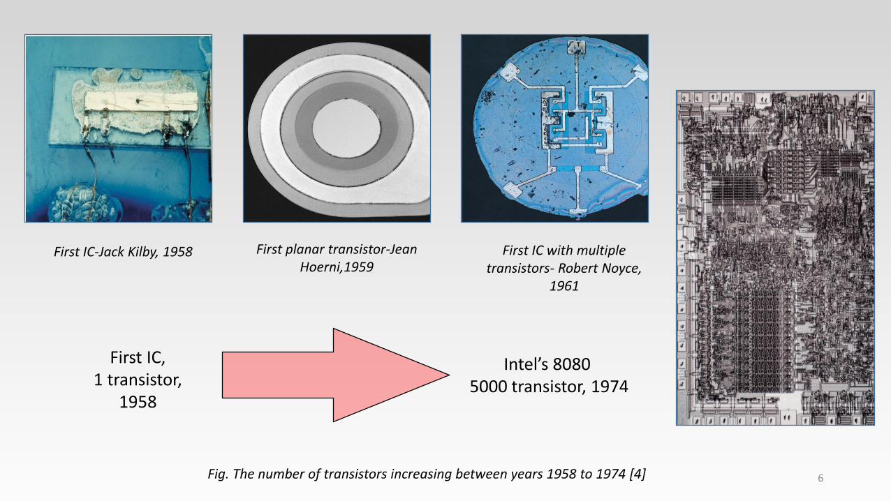
First IC, 1 transistor,
1958
Intel’s 80805000 transistor, 1974
Fig. The number of transistors increasing between years 1958 to 1974 [4] 6
First IC-Jack Kilby, 1958 First planar transistor-Jean Hoerni,1959
First IC with multiple transistors- Robert Noyce,
1961
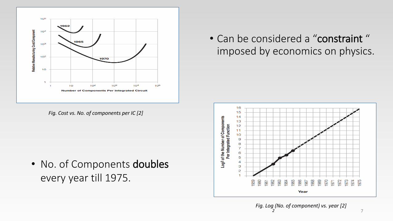
• Can be considered a “constraint “ imposed by economics on physics.
Fig. Cost vs. No. of components per IC [2]
7
• No. of Components doublesevery year till 1975.
Fig. Log (No. of component) vs. year [2] 2
8
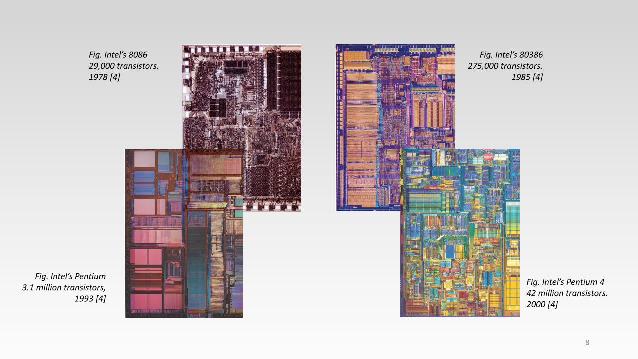
Fig. Intel’s 808629,000 transistors.1978 [4]
Fig. Intel’s 80386275,000 transistors.
1985 [4]
Fig. Intel’s Pentium 3.1 million transistors,
1993 [4]
Fig. Intel’s Pentium 442 million transistors.2000 [4]
9
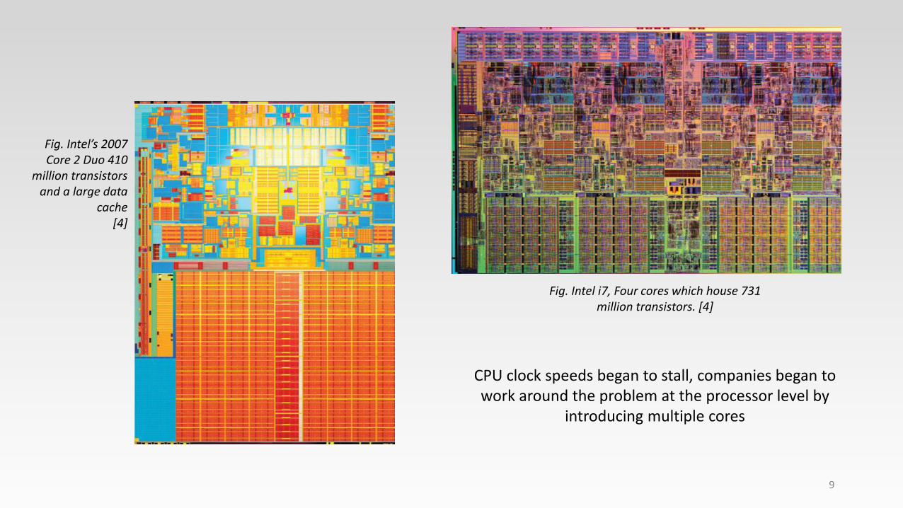
CPU clock speeds began to stall, companies began to work around the problem at the processor level by
introducing multiple cores
Fig. Intel i7, Four cores which house 731 million transistors. [4]
Fig. Intel’s 2007 Core 2 Duo 410
million transistors and a large data
cache[4]
The Technical Drivers
10
• Minimum feature sizes decreasing by about 10%, resulting in an increase in transistors per area of 25%
• Chip area was increasing by about 20%.
• Design cleverness made up the rest of the improvement , 33%.
1.25 x 1.20 x 1.33 = 2
Revised slope!
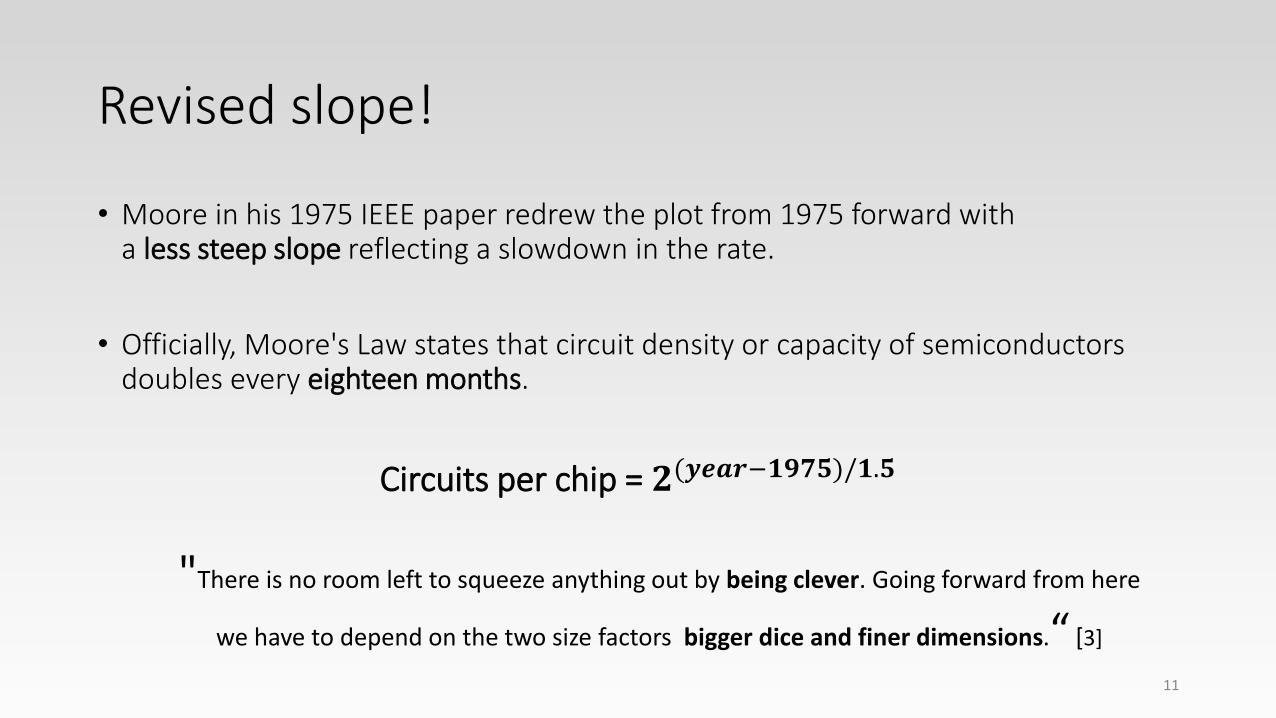
• Moore in his 1975 IEEE paper redrew the plot from 1975 forward witha less steep slope reflecting a slowdown in the rate.
• Officially, Moore's Law states that circuit density or capacity of semiconductors doubles every eighteen months.
Circuits per chip = 𝟐(𝒚𝒆𝒂𝒓−𝟏𝟗𝟕𝟓)/𝟏.𝟓
11
"There is no room left to squeeze anything out by being clever. Going forward from here
we have to depend on the two size factors bigger dice and finer dimensions.“ [3]

12
How do we keep pace ?
Fin-FET and UTB SOI
• Planar transistor- it is very difficult to reduce leakage current in a transistor when it’s very small.
• 3D ridge channel draped by the gate ,which switches the transistor on and off, is called a fin.
• SOI has a layer of insulator with a thin layer of silicon on top. Because, the current carrying channel is very thin, gate voltage can be scaled down.
• Higher gate voltages are made to make the difference between on and off more profound, but power is proportional to the square of the voltage.
13
Fin-FET vs. UTB SOI
Fin-FET UTB SOI
Fin-FETs need more manufacturing and design
UTBs need less manufacturing and design
First to the market. “Soitec” is increasingly investing
in on SOI technology.
With wider channel more current flows through, hence
faster.
The flat channel—with such thin silicon, less current goes
through, which translates to lower speed.
More costly to manufacture.But, companies like Intel are
funding in on Fin-FETs
The special UTB wafer are more costly, but the manufacture cost
on the company is low.
Fig. FinFET
Fig. UTB SOI
14
III-V Compounds
• Replace the current-carrying silicon channel with germanium and compound semiconductors known as III-Vs.
• The atoms in the alternative semiconductors are spaced farther apart than in silicon, making the crystals difficult to grow.
• The resulting chips could trim energy consumption at data centers, boost the battery life of mobile devices
15
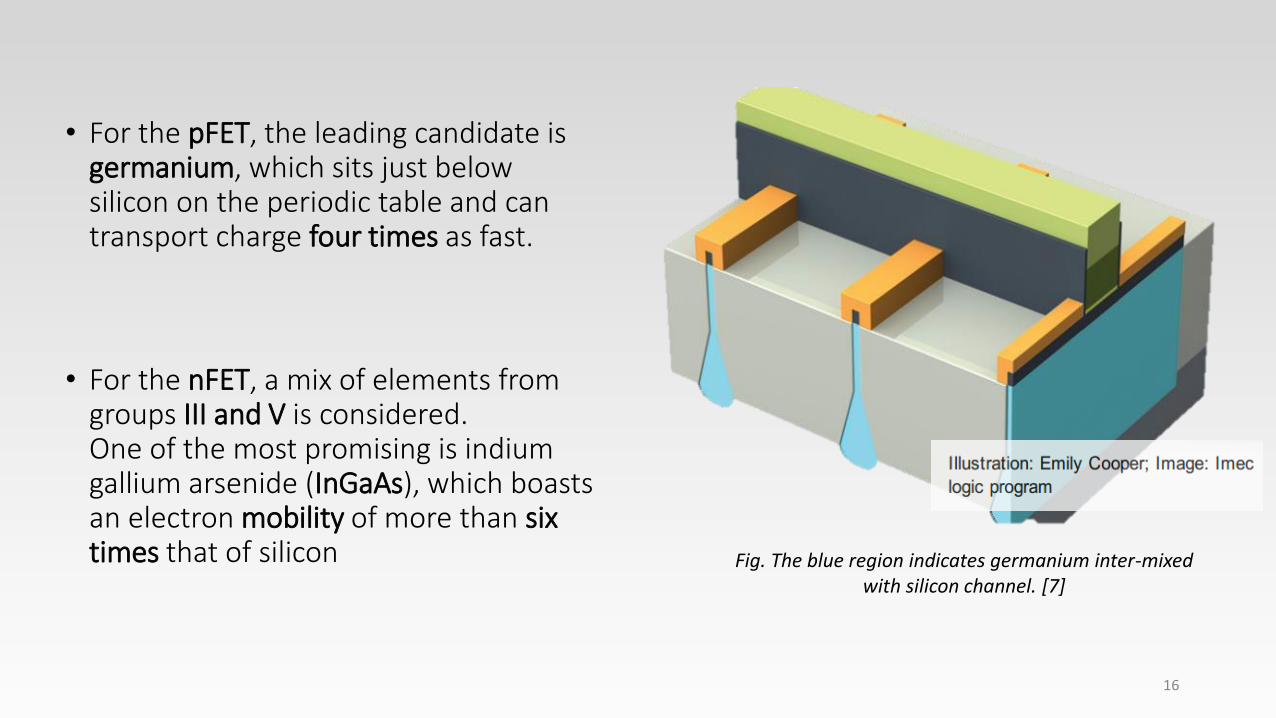
• For the pFET, the leading candidate is germanium, which sits just below silicon on the periodic table and can transport charge four times as fast.
• For the nFET, a mix of elements from groups III and V is considered.One of the most promising is indium gallium arsenide (InGaAs), which boasts an electron mobility of more than six times that of silicon
16
Fig. The blue region indicates germanium inter-mixed with silicon channel. [7]

High-K Metal Dielectric
17
Problems Solutions
Carriers tunneling the dielectric Thick dielectric medium
Uneven dielectric surface traps charges Atomic Layer deposition
Phonons scatter electrons in the channel Metal gate’s higher electron density
prevents scattering of electrons
Poor bonding between dielectric and gate causing poor gate field.
Proprietary metal used solves the bonding issues.
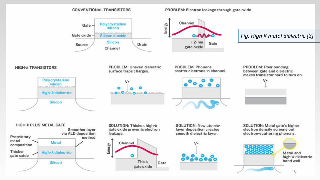
18
Fig. High K metal dielectric [3]

19
Future of Moore’s law…
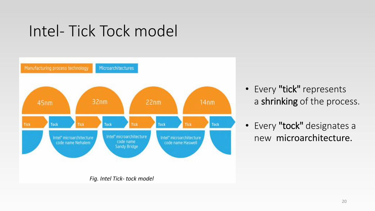
Intel- Tick Tock model
20
• Every "tick" represents a shrinking of the process.
• Every "tock" designates a new microarchitecture.
Fig. Intel Tick- tock model
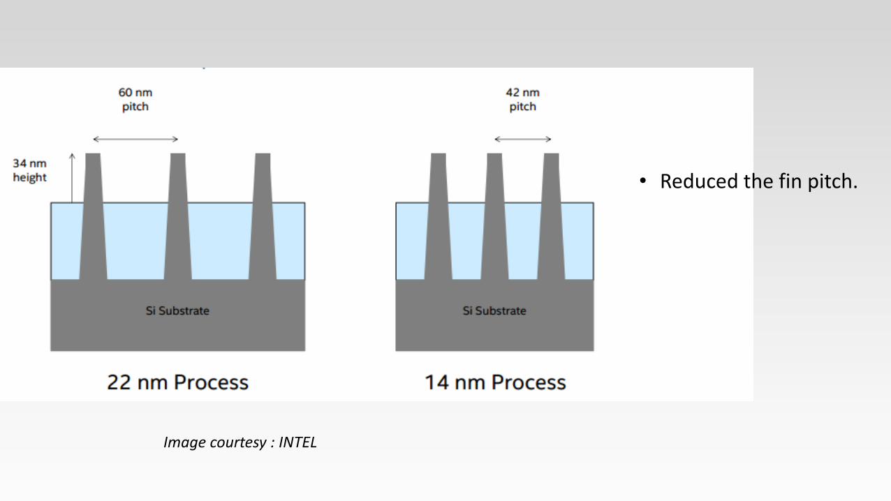
• Reduced the fin pitch.
Image courtesy : INTEL
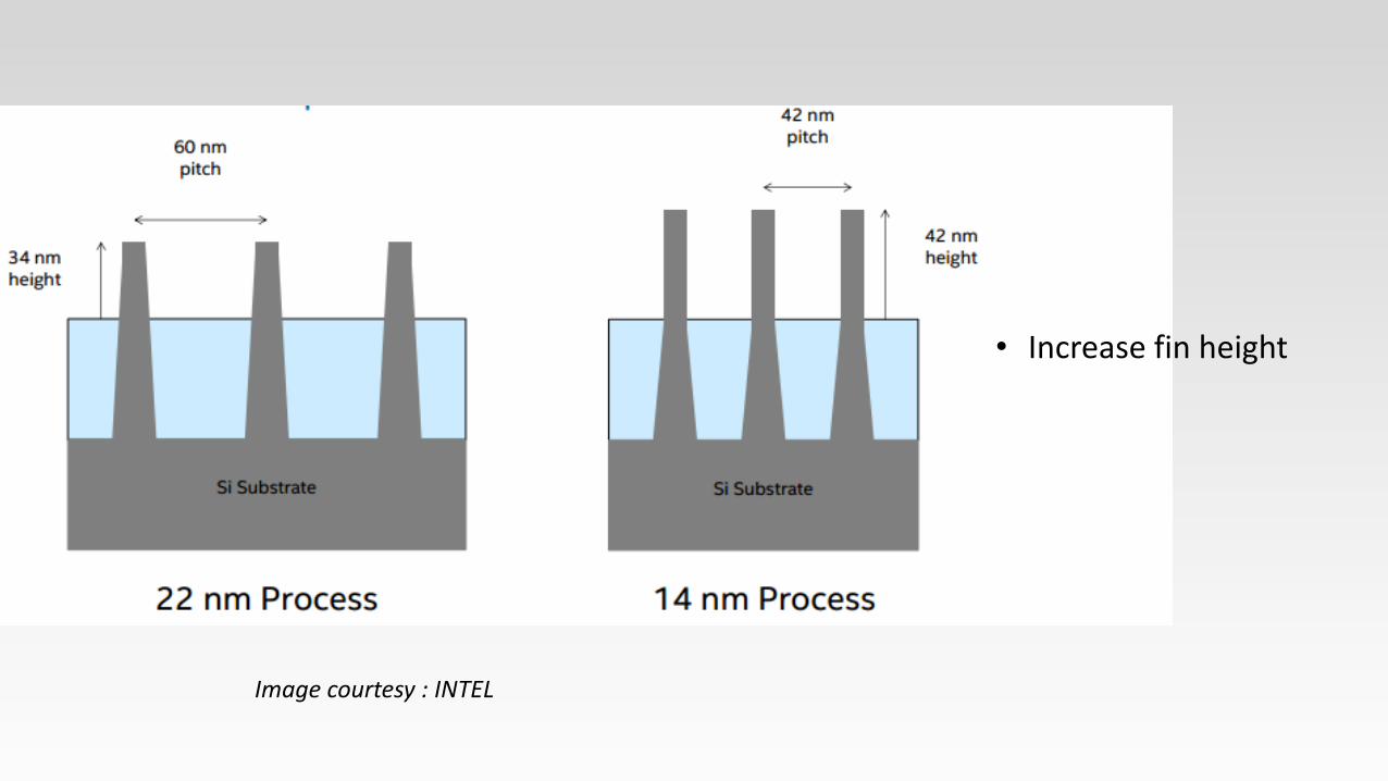
• Increase fin height
Image courtesy : INTEL
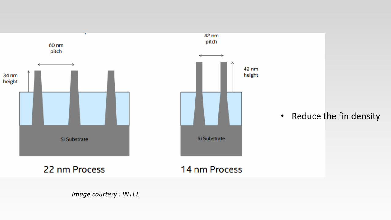
• Reduce the fin density
Image courtesy : INTEL
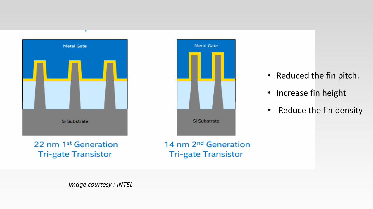
• Reduced the fin pitch.
• Increase fin height
• Reduce the fin density
Image courtesy : INTEL
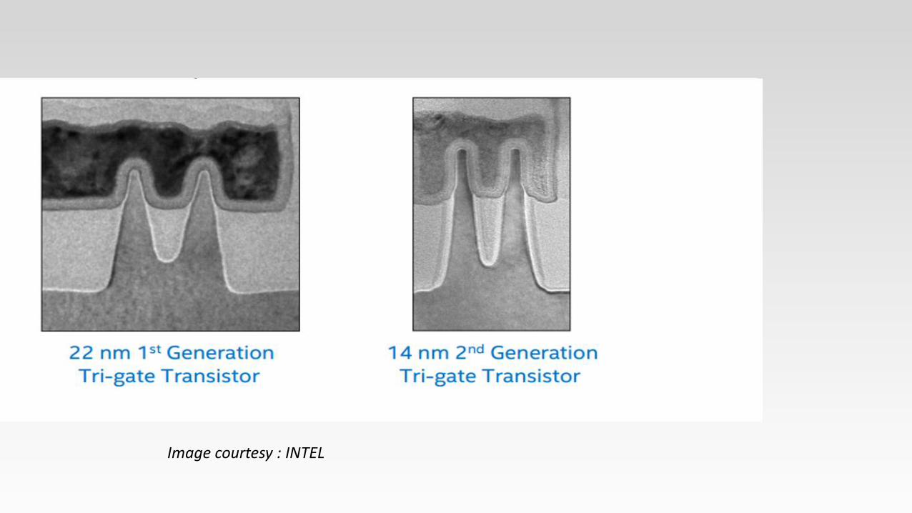
Image courtesy : INTEL

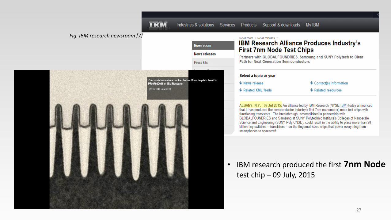
IBM 7nm Technology
26
• IBM Invested $3 billion dollar on research in July 2014
27
• IBM research produced the first 7nm Node test chip – 09 July, 2015
Fig. IBM research newsroom [7]
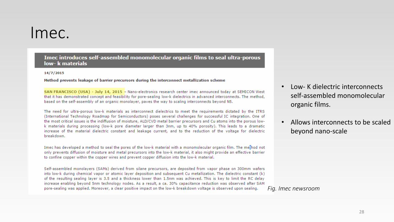
Imec.
28
• Low- K dielectric interconnects self-assembled monomolecular organic films.
• Allows interconnects to be scaled beyond nano-scale
Fig. Imec newsroom
Conclusions
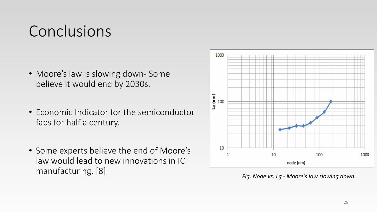
• Moore’s law is slowing down- Some believe it would end by 2030s.
• Economic Indicator for the semiconductor fabs for half a century.
• Some experts believe the end of Moore’s law would lead to new innovations in IC manufacturing. [8]
29
Fig. Node vs. Lg - Moore’s law slowing down
“ What can happen, will happen… “
30
Murphy’s Law :

References:[1] Chris A. Mac, “Fifty Years of Moore’s Law”, IEEE TRANSACTIONS ON SEMICONDUCTOR
MANUFACTURING, VOL. 24, NO. 2, MAY 2011
[2] Gordon E. Moore, “Cramming more components onto integrated circuits”, Electronics Magazine,
Volume 38 ,Number 8 , April 19 ,1965.
[3] Mark T. Bohr, Robert S. Chau, Tahir Ghani, Kaizad Mistry, “The Highk Solution”, IEEE Spectrum article,Oct 2007
[4] Kristina Grifantini,” Moore's Law”, MIT Technology Review article, December 22, 2008.
[5] Richard Stevenson, “Changing the Transistor Channel”, IEEE Spectrum article, Jun 2013
[6] www.intel.com
[7] http://www-03.ibm.com/press/us/en/pressrelease/47301.wss?ccy=us
[8] Agam Shah,”Lapsing of Moore's Law opens up opportunity in chip design”, PC World article, Aug 2013.
[9] Jamil Kawa,” FinFET Design, Manufacturability, and Reliability”, Synopsys DesignWare Technical Bulletin , Jan 2013.
[10] Bich-Yen Nguyen, George Celler, and Carlos Mazuré, “A Review of SOI Technology and its Applications”, SOITEC article, Pg. 51, Aug 2009.
[11] Bob Schaller, “The Origin, Nature, and Implications of MOORE'S LAW “, The Benchmark ofProgressin Semiconductor Electronics, Microsoft Research paper, Sept, 1996
31

32
Thank you !