26 - talking electronicstalkingelectronics.com/download ebooks/principles of...
TRANSCRIPT

Digital Electronics 729
26.1 Analog and Digital Signals
26.3 Binary Number System
26.5 Decimal to Binary Conversion
26.7 Octal Number System
26.9 Binary-Coded Decimal Code(BCD Code)
26.11 Three Basic Logic Gates
26.13 AND Gate
26.15 Combination of Basic LogicGates
26.17 Exclusive OR Gate
26.19 Advantages and Disadvan-tages of Digital Electronics
26.21 Boolean Theorems
26.23 Operator Precedence
26.25 Boolean Expressions forCombinational Logic Circuits
26.27 Truth Table from Logic Cir-cuit
26.29 Sum-of-Products Form
26.31 Binary Addition
26.33 Flip - Flops
○ ○ ○ ○ ○ ○ ○ ○ ○ ○ ○ ○ ○ ○ ○ ○ ○ ○ ○ ○ ○ ○ ○ ○ ○ ○ ○
INTRINTRINTRINTRINTRODUCTIONODUCTIONODUCTIONODUCTIONODUCTION
A continuously varying signal (voltage or cur-rent) is called an analog signal. For example,a sinusoidal voltage is an analog signal. In the
previous chapter, we studied the behaviour of diodesand transistors primarily from the analog or continuous-signal point of view. In an analog electronic circuit, theoutput voltage changes continuously according to theinput voltage variations. In other words, the outputvoltage can have an infinite number of values. A signal(voltage or current) which can have only two discretevalues is called a digital signal. For example, a squarewave is a digital signal. The semiconductors devices(e.g. diodes, transistors etc.) can be designed for two-state operation viz., saturation and cut off. In that case,the output voltage can have only two states (i.e., values),either *low or high. An electronic circuit that is de-signed for two-state operation is called a digital circuit.
* The exact value of voltage is unimportant if the voltageis distinguishable as low or high.
Digital Electronics
26

730 Principles of Electronics
The branch of electronics which deals with digital circuits is called digital electronics. Whenmost of us hear the term digital, we immediately think of “digital calculator” or “digital computer”.This is attributed to the dramatic way the low-cost, powerful calculators and computers have becomeaccessible to an average person. Now digital circuits are being used in many electronic products suchas video games, microwave ovens and oscilloscopes. Digital techniques have also replaced a lot ofthe older “analog circuits” used in consumer products such as radios, TV sets and high-fidelity soundrecording and playback equipment. In this chapter, we shall discuss the fundamental aspects ofdigital electronics.
26.1 Analog and Digital Signals(i) Analog signal. A continuously varying signal (voltage or current) is called an analog sig-
nal. For example, an alternating voltage varying sinusoidally is an analog signal [See Fig. 26.1]. Ifsuch an analog signal is applied to the input of a transistor amplifier, the output voltage will also varysinusoidally. This is the analog operation i.e., the output voltage can have an infinite number ofvalues. Due to many-valued output, the analog operation is less reliable.
(ii) Digital signal. A signal (voltage or current) that can have only two discrete values is called adigital signal. For example, a square wave is a digital signal [See Fig. 26.2]. It is because this signal hasonly two values viz, +5 V and 0 V and no other value. These values are labelled as High and Low. TheHigh voltage is + 5 V and the Low voltage is 0 V. If proper digital signal is applied to the input of atransistor, the transistor can be driven between cut off and saturation. In other words, the transistor willhave two-state operations i.e., output is either low or high. Since digital operation has only two states(i.e., ON or OFF), it is far more reliable than many-valued analog operation. It is because with two-states operation, all the signals are easily recognised as either low or high.
Fig. 26.1 Fig. 26.2
26.2 Digital CircuitAn electronic circuit that handles only a digital signal is called a digital circuit.
The output voltage of a digital circuit is either low or high and no other value. In other words,digital operation is a two-state operation. These states are expressed as (High or Low) or (ON orOFF) or (1 or 0). Therefore, a digital circuit is one that expresses the values in digits 1’s or 0’s.Hence the name digital. The numbering concept that uses only the two digits 1 and 0 is the binarynumbering system. Therefore, the first step would be to discuss this number system.
26.3 Binary Number SystemA number system is a code that uses symbols to count the number of items. The most common andfamiliar number system is the decimal number system. The decimal number system uses the symbols0, 1, 2, 3, 4, 5, 6, 7, 8 and 9. Thus, the decimal system uses 10 digits for counting the items. A binarysystem uses only two digits (0 and 1) for counting the items. The reader may wonder how to count theitems in a binary system. Let us see how it is done.

Digital Electronics 731Counting in Decimal and Binary systems. Figure 26.3 shows the counting of stones in deci-
mal as well as binary system. As you will see, the counting in the binary number system is performedmuch the same way as in the decimal number system.
Stones Decimal BinaryNo stone 0 0••••• 1 1• •• •• •• •• • 2 10• • •• • •• • •• • •• • • 3 11• • • •• • • •• • • •• • • •• • • • 4 100• • • • •• • • • •• • • • •• • • • •• • • • • 5 101• • • • • •• • • • • •• • • • • •• • • • • •• • • • • • 6 110• • • • • • •• • • • • • •• • • • • • •• • • • • • •• • • • • • • 7 111• • • • • • • •• • • • • • • •• • • • • • • •• • • • • • • •• • • • • • • • 8 1000• • • • • • • • •• • • • • • • • •• • • • • • • • •• • • • • • • • •• • • • • • • • • 9 1001
Fig. 26.3
(i) Let us first see how items are counted in decimal system. In this system, the count starts as0, 1, ...., 9. After 9, we are to write the next number. To do so, we use the second digit of the decimalsystem (i.e., 1) followed by the first digit (i.e., 0). So after 9, the next number is 10. The count againcontinues as 10, 11, 12 ....., 19. After 19, we use the third digit of the system (i.e., 2) followed by thefirst digit (i.e., 0) and the count continues as 20, 21, .... etc. In this way, we get the number upto 99.In order to represent a number next to 99, we use three decimal digits (100). That is to say seconddigit of the decimal system (i.e., 1) followed by two first digits (i.e, two zeros).
(ii) Let us now turn to binary system. Note that 0 and 1 count in the binary system is the same asin the decimal counting. To represent 2 stones, we use the second binary digit (i.e., 1) followed by thefirst (i.e., 0). This gives binary number 10 (read as one-zero and not ten) as an equivalent of 2 in thedecimal system. Likewise, 3 in the decimal system can be represented by the binary number 11 (readas one-one and not eleven). After this, the two binary digits are exhausted. We shall use three digitsto represent the next binary number. Thus, to represent 4 (four), we use the second binary digitfollowed by two first binary digits. This gives the binary *100 (read as one-zero-zero) as equivalentto 4 in the decimal system. Here is a simple way to find binary equivalents. Each time the two digits1 and 0 in one position are exhausted (counted as high as they will go), a 1 is added at the left, alldigits to the right are made 0, and the count continues. The reader may apply this simple rule to findnext binary numbers.Notes :
(i) Each binary digit (0 or 1) is referred to as a bit. A string of four bits is called as a nibble andeight bits make a byte. Thus, 1001 is a nibble and 10010110 is a binary byte.
(ii) The binary number system is the most useful in digital circuits because there are only twodigits (0 and 1).
26.4 Place ValueConsider the decimal number 642. This can be expressed as :
642 = 600 + 40 + 2Note that in a multidigit decimal number (i.e., 642 in the present case), each position has a value
that is 10 times the value of the next position to its immediate right. In other words, every positioncan be expressed as :
* Note that the procedure is similar to that which was used to write 100 (hundred) in the decimal system.○ ○ ○ ○ ○ ○ ○ ○ ○ ○ ○ ○ ○ ○ ○ ○ ○ ○ ○ ○ ○ ○ ○ ○ ○ ○ ○ ○ ○ ○ ○ ○ ○ ○ ○ ○ ○ ○ ○ ○ ○ ○ ○ ○ ○ ○ ○ ○ ○

732 Principles of Electronics
642 = 6 × 10² + 4 × 101 + 2 × 100
Thus, we find that values of various positions in a decimal number system are powers of 10 i.e.,equal to the number of digits used in the system. This number is called base or radix of the system.Thus, the decimal system has base of 10 (ten).
For the decimals, the digit to the extreme right is referred to as the least significant digit (LSD)because its positional value or weight is the lowest. For the decimal number 642, 2 is the LSD. Theleft-most digit in the decimal number is the most significant digit (MSD) because its positional valueor weight is the highest. For the decimal number 642, 6 is the MSD with a value of 600.
Binary number system. In the binary number system, only two digits (0 and 1) are used. There-fore, the base of this system is 2. In a binary number, each position has a value that is 2 times thevalue of the next position to its immediate right. In other words, every position can be expressed by2 raised to some power. We know that binary number 1001 is equal to the decimal number 9. Thiscan be readily shown as under :
1001 = 1 × 23 + 0 × 22 + 0 × 21 + 1 × 20 = 9For binary numbers, the digit at the extreme right is referred to as least significant bit (LSB).
In the binary number 1001, the 1 at the right is the LSB. The left-most digit is called the mostsignificant bit (MSB). In the binary number 1001, the 1 at the left is the MSB with the value of 8 indecimal terms.26.5 Decimal to Binary ConversionThere are many methods to perform this conversion. The method described here is called double-dabble because it requires successive divisions by 2. This method can be summarised as under :
Divide progressively the decimal number by 2 and write down the remainder after each division.Continue this process till you get a quotient of 0 and remainder of 1, the conversion is now complete.The remainders, taken in reverse order, form the binary number [See Fig. 26.4].
Note that 13 is first divided by 2, giving a quotient of 6 with a remainder of 1. This remainderbecomes the 20 position in the binary number. The 6 is then divided by 2, giving a quotient of 3 witha remainder of 0. This remainder becomes the 21 position in the binary number.
Continuing this procedure, the equivalent binary number is 1101.Decimal number↓13 ÷ 2 = 6 with a remainder of 1 20 ↑ LSB6 ÷ 2 = 3 with a remainder of 0 21
3 ÷ 2 = 1 with a remainder of 1 22
1 ÷ 2 = 0 with a remainder of 1 23 MSB
Fig. 26.4
Example 26.1. Convert the decimal number 37 to its equivalent binarynumber.
Solution. Using double-dabble method, we find that the equivalent binarynumber is 100101. It is a usual practice to mention the base of the number system.The decimal system has a base of 10 while binary system has a base of 2.
∴ (37)10 = (100101)2Note. This notation avoids the confusion that may arise because decimal
number also involves the digits 0 and 1. Thus, (101)10 denotes the decimal numberhundred one while the binary number (101)2 is equivalent to decimal number 5.
2 372 18 − 12 9 − 02 4 − 12 2 − 02 1 − 0
0 − 1

Digital Electronics 733Example 26.2. Convert the decimal number 23 to its equivalent binary number.Solution. Using double-dabble method, we find that the equivalent binary number is 10111.∴ (23)10 = (10111)2Note that binary number 10111 has five bits.
26.6 Binary to Decimal ConversionBinary numbers can be converted to equivalent decimal numbers quite easily. Sup-pose you are given the binary number 110011. Its conversion to equivalent deci-mal number involves the following two steps :
(i) Place the decimal value of each position of the binary number.(ii) Add all the decimal values to get the decimal number.Thus, (110011)2 = 1 × 25 + 1 × 24 + 0 × 23 + 0 × 22 + 1 × 21 + 1 × 20
= 32 + 16 + 0 + 0 + 2 + 1 = 51∴ (110011)2 = (51)10Note. In binary to decimal conversion, all positions containing 0 can be ignored. Only add the
decimal values of the positions where 1 appears. Thus, in case of the above binary number,(110011)2 = 1 × 25 + 1 × 24 + 1 × 21 + 1 × 20
= 32 + 16 + 2 + 1 = 51Example 26.3. Convert the binary number 110001 to its equivalent decimal number.Solution. The binary number along with its decimal values of various positions is shown.∴ (110001)2 = 1 × 25 + 1 × 24 + 1 × 20 1 1 0 0 0 1
= 32 + 16 + 1 = 49 25 24 23 22 21 20
or (110001)2 = (49)10
26.7 Octal Number SystemThe octal number system has a radix of eight so that it uses eight digits : 0, 1, 2, 3, 4, 5, 6 and 7. Theposition weights in the system are powers of eight. The digit positions of first six powers of eight are:
80 = 1 ; 81 = 8 ; 82 = 6483 = 512 ; 84 = 4096 ; 85 = 32768
The octal number system is frequently used in digital circuits due to two principal reasons. First,it can be easily converted to binary. Secondly, there are significantly fewer digits in any given octal numberthan in the corresponding binary number so that it is much easier to work with shorter octal numbers.
1. Decimal-to-Octal Conversion. To convert a decimal number to octal, we employ the samerepeated-division method that we used in decimal-to-binary conversion. However, here the divisionfactor is 8 instead of two. The following examples illustrate decimal-to-octal conversion.
(i) To convert decimal number 91 to octal number, the procedure is as under :Division Remainder
91 ÷ 8 = 11 3 (LSB)11 ÷ 8 = 1 31 ÷ 8 = 0 1 (MSB)
∴ (91)10 = (133)8(ii) As another example, consider the conversion of decimal number 266 to octal number.
Division Remainder266 ÷ 8 = 33 2 (LSB)
33 ÷ 8 = 4 1
1 1 0 0 1 125 24 23 22 21 20
2 232 11 − 12 5 − 12 2 − 12 1 − 0
0 − 1
734 Principles of Electronics
4 ÷ 8 = 0 4 (MSB)∴ (266)10 = (412)82. Octal-to-Decimal Conversion. An octal-to-decimal conversion can be done in the same
manner as a binary-to-decimal conversion i.e. simply add up the position weights to obtain the deci-mal number. The following examples illustrate octal-to-decimal conversion.
(i) To convert octal number (133)8 to decimal number, the procedure is as under :Position weights 82 81 80
Octal number 1 3 3∴ (133)8 = (82 × 1) + (81 × 3) + (80 × 3)
= 64 + 24 + 3 = 91∴ (133)8 = (91)10(ii) As another example, consider the conversion of octal number (372)8 to decimal number.
Position weights 82 81 80
Octal number 3 7 2∴ (372)8 = (82 × 3) + (81 × 7) + (80 × 2)
= 192 + 56 + 2 = 250∴ (372)8 = (250)103. Octal-to-Binary Conversion. The advantage of oc-
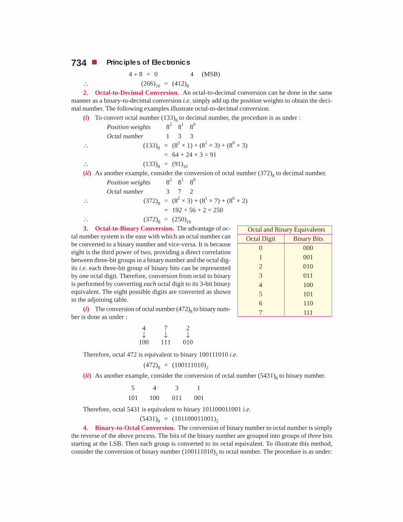
tal number system is the ease with which an octal number canbe converted to a binary number and vice-versa. It is becauseeight is the third power of two, providing a direct correlationbetween three-bit groups in a binary number and the octal dig-its i.e. each three-bit group of binary bits can be representedby one octal digit. Therefore, conversion from octal to binaryis performed by converting each octal digit to its 3-bit binaryequivalent. The eight possible digits are converted as shownin the adjoining table.
(i) The conversion of octal number (472)8 to binary num-ber is done as under :
4 7 2
100 111 010↓ ↓ ↓
Therefore, octal 472 is equivalent to binary 100111010 i.e.(472)8 = (100111010)2
(ii) As another example, consider the conversion of octal number (5431)8 to binary number.
5 4 3 1101 100 011 001
Therefore, octal 5431 is equivalent to binary 101100011001 i.e.(5431)8 = (101100011001)2
4. Binary-to-Octal Conversion. The conversion of binary number to octal number is simplythe reverse of the above process. The bits of the binary number are grouped into groups of three bitsstarting at the LSB. Then each group is converted to its octal equivalent. To illustrate this method,consider the conversion of binary number (100111010)2 to octal number. The procedure is as under:
Octal and Binary EquivalentsOctal Digit Binary Bits
0 0001 0012 0103 0114 1005 1016 1107 111

Digital Electronics 735� � �100 111 010
4 7 2↓ ↓ ↓
∴ (100111010)2 = (472)8Note that there are fewer digits in the octal number than in the corresponding binary number.
Therefore, it is much easier to work with shorter octal numbers.Sometimes the binary number will not have even groups of 3 bits. In that case, we can add one or
two 0s to the left of the MSB of the binary number to fill the last group. This point is illustrated belowfor the binary number 11010110.
� � �011 010 110
3 2 6Note that a 0 is placed to the left of the MSB to produce even groups of 3 bits.Example 26.4. Convert the following decimal numbers to octal equivalent.(i) 76 (ii) 255 (iii) 372Solution.(i) Division Remainder
76 ÷ 8 = 9 4 (LSB)9 ÷ 8 = 1 11 ÷ 8 = 0 1 (MSB)
∴ (76)10 = (114)8(ii) Division Remainder
255 ÷ 8 = 31 7 (LSB)31 ÷ 8 = 3 7
3 ÷ 8 = 0 3 (MSB)∴ (255)10 = (377)8(iii) Division Remainder
372 ÷ 8 = 46 4 (LSB)46 ÷ 8 = 5 6
5 ÷ 8 = 0 5 (MSB)∴ (372)10 = (564)8
Example 26.5. Convert octal number (24.6)8 to the equivalent decimal number.Solution.
(24.6)8 = (2 × 81) + (4 × 80) + (6 × 8– 1)= 16 + 4 + 0.75 = 20.75
∴ (24.6)8 = (20.75)10
Example 26.6. Convert (177)10 to its 8-bit binary equivalent by first converting to octal.Solution. We shall first convert (177)10 to its equivalent octal number as under :
Division Remainder177 ÷ 8 = 22 1 (LSB)
22 ÷ 8 = 2 62 ÷ 8 = 0 2 (MSB)
∴ (177)10 = (261)8We now convert the octal number (261)8 to its equivalent binary number as under :

736 Principles of Electronics2 6 1
010 110 001↓ ↓ ↓
Therefore, the binary equivalent is 010110001. We remove the leading zero to express the resultas 8 bits
∴ (177)10 = (10110001)2
26.8 Hexadecimal Number SystemThe hexadecimal system uses a radix of 16. Therefore,it has 16 possible digit symbols. The first ten digits inthe hexadecimal system are represented by the num-bers 0 through 9 (0, 1, 2, 3, 4, 5, 6, 7, 8 and 9) and theletters A though F are used to represent the numbers10, 11, 12, 13, 14 and 15 respectively. The adjoiningtable shows the relationships among hexadecimal, deci-mal and binary. Note that each hexadecimal digit rep-resents a group of four binary digits.
As is true for binary and decimal numbers, eachdigit in the hexadecimal system has a positional valueor weight. For the right most digit of a hex (abbrevia-tion for hexadecimal) number, the positional weight is160 (= 1), the next digit to the left has a positional weightof 161 (= 16) and so on. The positional weight distribu-tion of a hex number system is given below:
etc.3 2 1 016 16 16 16
4096 256 16 1
1. Decimal-to-Hex Conversion. To convert adecimal number to hex number, the technique is the same as used for decimal-to-binary conversion ordecimal-to-octal conversion. Recall that we did decimal-to-binary conversion using repeated divi-sion by 2 and decimal-to-octal conversion using repeated division by 8. Likewise, decimal-to-hexconversion is done using repeated division by 16. Let us illustrate the decimal-to-hex conversionprocedure. Suppose we are to convert the decimal number 423 to hex number.
Division Remainder423 ÷ 16 = 26 7 (LSB)
26 ÷ 16 = 1 101 ÷ 16 = 0 1 (MSB)
∴ (423)10 = (1 A7)16Note that 10 is represented by the letter A.2. Hex-to-Decimal Conversion. In order to convert a hex number to its decimal equivalent,
simply add up the position weight of each digit in the hex number. The following example illustratesthis conversion.
(356)16 = (3 × 162) + (5 × 161) + (6 × 160)= 768 + 80 + 6 = 854
∴ (356)16 = (854)103. Hex-to-Binary Conversion. The conversion from hex to binary is performed by convert-
ing each hex digit to its 4-bit binary equivalent (See above table). The following example illustratesthis point. Here, we shall convert hex number (9 F2)16 to its binary equivalent.
Hexadecimal Decimal Binary0 0 00001 1 00012 2 00103 3 00114 4 01005 5 01016 6 01107 7 01118 8 10009 9 1001A 10 1010B 11 1011C 12 1100D 13 1101E 14 1110F 15 1111
←

Digital Electronics 7379 2
1001 1111 0010
F↓ ↓ ↓
∴ (9F2)16 = (100111110010)24. Binary-to-Hex Conversion. The conversion from binary to hex is just the reverse of the
above process. The binary number is grouped into groups of four bits and each group is converted toits equivalent hex digit. The following example illustrates this point. Here, we shall convert binarynumber (1110100110)2 to its *equivalent hex number.
� � �0011 1010 01103 6A
∴ (1110100110)2 = (3A6)16
Example 26.7. Convert decimal number 541 to hexadecimal.Solution.
Division Remainder541 ÷ 16 = 33 13 (LSB)
33 ÷ 16 = 2 12 ÷ 16 = 0 2 (MSB)
∴ (541)10 = (21D)16
Example 26.8. Convert decimal number 378 to a 16-bit number by first converting to hexa-decimal.
Solution.Division Remainder
378 ÷ 16 = 23 10 (LSB)23 ÷ 16 = 1 7
1 ÷ 16 = 0 1 (MSB)Thus (378)10 = (17A )16. We can easily convert this hex number to binary 000101111010. There-
fore, we can express (378)10 as a 16-bit binary number by adding four leading 0s.(378)10 = (0000000101111010)2
Example 26.9. Convert (B2F)16 to octal.Solution. It is easier to first convert hex to binary and then to octal.
(B2F)16 = 1011 0010 1111 .... conversion to binary= 101 100 101 111 .... 3-bit groupings= 5 4 5 7
∴ (B2F)16 = (5457)8
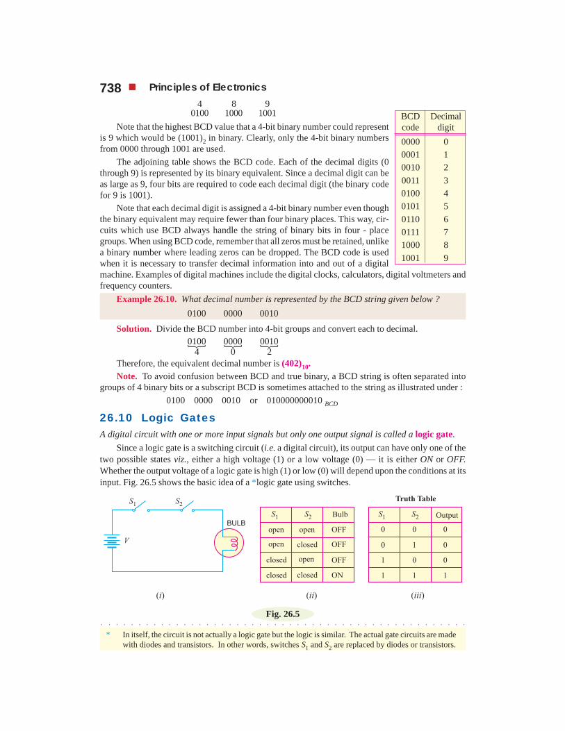
26.9. Binary-Coded Decimal Code (BCD Code)Circuits and machines can deal readily with binary numbers, but people are used to working withdecimal numbers. Moreover, there are considerably fewer decimal digits required to represent a num-ber than there are binary. It is much easier to remember just a few digits than it is to remember many.Thus whenever there is an interface between digital circuits and people, the interface data usuallytakes the decimal from. As a result, the digital circuits must utilise some binary code to convenientlyrepresent the decimal numbers. The code used for this purpose is called BCD code. In a BCD code,each decimal number is represented by a 4-bit binary number. For example, to convert decimalnumber (489)10 to BCD, the procedure is as under :
* Zeros are added, as needed, to complete 4-bit group.○ ○ ○ ○ ○ ○ ○ ○ ○ ○ ○ ○ ○ ○ ○ ○ ○ ○ ○ ○ ○ ○ ○ ○ ○ ○ ○ ○ ○ ○ ○ ○ ○ ○ ○ ○ ○ ○ ○ ○ ○ ○ ○ ○ ○ ○ ○ ○ ○
738 Principles of Electronics
4 8 90100 1000 1001
Note that the highest BCD value that a 4-bit binary number could representis 9 which would be (1001)2 in binary. Clearly, only the 4-bit binary numbersfrom 0000 through 1001 are used.
The adjoining table shows the BCD code. Each of the decimal digits (0through 9) is represented by its binary equivalent. Since a decimal digit can beas large as 9, four bits are required to code each decimal digit (the binary codefor 9 is 1001).
Note that each decimal digit is assigned a 4-bit binary number even thoughthe binary equivalent may require fewer than four binary places. This way, cir-cuits which use BCD always handle the string of binary bits in four - placegroups. When using BCD code, remember that all zeros must be retained, unlikea binary number where leading zeros can be dropped. The BCD code is usedwhen it is necessary to transfer decimal information into and out of a digitalmachine. Examples of digital machines include the digital clocks, calculators, digital voltmeters andfrequency counters.
Example 26.10. What decimal number is represented by the BCD string given below ?0100 0000 0010
Solution. Divide the BCD number into 4-bit groups and convert each to decimal.� � �0100 0000 0010
4 0 2Therefore, the equivalent decimal number is (402)10.Note. To avoid confusion between BCD and true binary, a BCD string is often separated into
groups of 4 binary bits or a subscript BCD is sometimes attached to the string as illustrated under :0100 0000 0010 or 010000000010 BCD
26.10 Logic GatesA digital circuit with one or more input signals but only one output signal is called a logic gate.
Since a logic gate is a switching circuit (i.e. a digital circuit), its output can have only one of thetwo possible states viz., either a high voltage (1) or a low voltage (0) — it is either ON or OFF.Whether the output voltage of a logic gate is high (1) or low (0) will depend upon the conditions at itsinput. Fig. 26.5 shows the basic idea of a *logic gate using switches.
Fig. 26.5
BCD Decimalcode digit0000 00001 10010 20011 30100 40101 50110 60111 71000 81001 9
* In itself, the circuit is not actually a logic gate but the logic is similar. The actual gate circuits are madewith diodes and transistors. In other words, switches S1 and S2 are replaced by diodes or transistors.
○ ○ ○ ○ ○ ○ ○ ○ ○ ○ ○ ○ ○ ○ ○ ○ ○ ○ ○ ○ ○ ○ ○ ○ ○ ○ ○ ○ ○ ○ ○ ○ ○ ○ ○ ○ ○ ○ ○ ○ ○ ○ ○ ○ ○ ○ ○ ○ ○

Digital Electronics 739(i) When S1 and S2 are open, the bulb is OFF.
(ii) When S1 is open and S2 closed, the bulb is OFF.(iii) When S2 is open and S1 closed, the bulb is OFF.(iv) When both S1 and S2 are closed, the bulb is ON.Note that output (OFF or ON) depends upon the conditions at the input.The four possible combinations of switches S1 and S2 are shown in the table on the previous
page. It is clear that when either of the switches (S1 or S2) or both are open, the bulb is OFF. In binarylanguage, when either of the inputs or both the inputs are low (0), the output is low. When bothswitches are closed, the bulb is ON. In terms of binary language, when both the inputs are high (1),the output is high. It is usual practice to show the conditions at the input and output of a logic gate inthe binary form as shown in the table on the previous page. Such a table is called truth table.The term “logic” is usually used to refer to a decision-making process. A logic gate makes logicaldecisions regarding the existence of output depending upon the nature of the input. Hence, suchcircuits are called logic circuits.
26.11 Three Basic Logic GatesA logic gate is a circuit that has one or more input signals but only one output signal. All logic gatescan be analysed by constructing a truth table. A truth table lists all input possibilities and the corre-sponding output for each input. The three basic logic gates that make up all digital circuits are (i) ORgate (ii) AND gate and (iii) NOT gate. We shall first discuss these three basic logic gates and then thecombination of these gates. The following points may be noted about logic *gates :
(i) A binary 0 represents 0 V and binary 1 represents + 5V**. It is common to refer to binary 0as LOW input or output and binary 1 as HIGH input or output.
(ii) A logic gate has only one output signal. The output will depend upon the input signal/signals and the type of gate.
(iii) The operation of a logic gate may be described either by truth table or Boolean algebra.
26.12 OR GateAn OR gate is a logic gate that has two or more inputs but only one output. However, the output Y ofan OR gate is LOW when all inputs are LOW. The output Y of an OR gate is HIGH if any or all theinputs are HIGH.
It is called OR gate because the output is high if any or all the inputs are high. For the samereason, an OR gate is sometimes called “any or all gate”. For example, consider a 2-input OR gate.The output Y will be high if either or both inputs are high.
OR gate operation. Fig. 26.6 (i) shows one way to build a 2-input OR gate while Fig. †26.6 (ii)shows its simplified schematic diagram. The input voltages are labeled as A and B while the outputvoltage is Y. Note that negative terminal of the battery is grounded and corresponds to 0 state (LOWlevel). The positive terminal of the battery (+5 V) corresponds to 1 state (HIGH level). There areonly four input-output possibilities.
* A gate can be regarded as a barrier which when closed prevents the passgae of information but if openallows the signal/signals to pass through freely.
** In digital systems, the binary information is represented by two voltage levels, generally +5 V and 0 V.So 5 V is used to represent binary 1 and 0 V is used to represent binary 0.
† As you can see in Fig. 26.6 (ii) that output is high when either or both of the input switches are closedbut not when both are open.
○ ○ ○ ○ ○ ○ ○ ○ ○ ○ ○ ○ ○ ○ ○ ○ ○ ○ ○ ○ ○ ○ ○ ○ ○ ○ ○ ○ ○ ○ ○ ○ ○ ○ ○ ○ ○ ○ ○ ○ ○ ○ ○ ○ ○ ○ ○ ○ ○

740 Principles of Electronics
(i) When both A and B are connected to ground, both diodes are non-conducting. Hence, theoutput voltage is ideally zero (low voltage). In terms of binary, when A = 0 and B = 0, then Y = 0 asshown in the truth table in Fig. 26.6 (iii).
Fig. 26.6
(ii) When A is connected to ground and B connected to the positive terminal of the battery, diodeD2 is forward biased and diode D1 is non-conducting. Therefore, diode D2 conducts and the outputvoltage is ideally +5 V. In terms of binary, when A = 0 and B = 1, then Y = 1 [See Fig. 26.6 (iii)].
(iii) When A is connected to the positive terminal of the battery and B to the ground, diode D1 ison and diode D2 is off. Again the output voltage is +5 V. In binary terms, when A = 1 and B = 0, thenY = 1 [See Fig. 26.6 (iii)].
(iv) When both A and B are connected to the positive terminal of the battery, both diodes are on.Since the diodes are in parallel, the output voltage is +5 V. In binary terms, when A = 1 and B = 1, thenY = 1 [See Fig. 26.6 (iii)].
It is clear from the truth table that for OR gate, the out-put is high if any or all of the inputs are high. The only way toget a low output is by having all inputs low. Fig. 26.7 showsthe logic symbol of OR gate. Note that the symbol has curvedline at the input.Boolean expression. The algebra used
to symbolically describe logic functions is called Boolean algebra. The “+” signin Boolean algebra refers to the logical OR function. The Boolean expressionfor OR function is
A + B = Y↑
OR symbolThe adjoining table shows possibilities for the inputs. According to this table, when 0 is ORed
with 0, the result equals 0. Also, any variable ORed with 1 equals 1. The OR function can be summedup as under :
0 ORed with 0 equals 00 ORed with 1 equals 11 ORed with 1 equals 1
26.13 AND GateThe AND gate is a logic gate that has two or more inputs but only one output. The output Y of ANDgate is HIGH when all inputs are HIGH. However, the output Y of AND gate is LOW if any or allinputs are LOW.
A + B = Y0 + 0 = 00 + 1 = 11 + 0 = 11 + 1 = 1
Fig. 26.7

Digital Electronics 741It is called AND gate because output is HIGH only when all the inputs are HIGH. For this
reason, the AND gate is sometimes called “all or nothing gate”. For example, consider a 2-inputAND gate. The output will be HIGH when both the inputs are HIGH.
AND gate operation. Fig. 26.8 (i) shows one way to build a 2-input AND gate while *Fig. 26.8(ii) shows its simplified schematic diagram. There are only four input-output possibilities.
Fig. 26.8
(i) When both A and B are connected to ground, both the diodes (D1 and D2) are forward biasedand hence they conduct current. Consequently, the two diodes are grounded and output voltage is zero.In terms of binary, when A = 0 and B = 0, then Y = 0 as shown in truth table in Fig. 26.8 (iii).
(ii) When A is connected to the ground and B connected to the positive terminal of the battery,diode D1 is forward biased while diode D2 will not conduct. Therefore, diode D1 conducts and isgrounded. Again output voltage will be zero. In binary terms, when A = 0 and B = 1, then Y = 0. Thisfact is shown in the truth table.
(iii) When B is connected to the ground and A connected to the positive terminal of the battery,the roles of diodes are interchanged. Now diode D2 will conduct while diode D1 does not conduct.As a result, diode D2 is grounded and again output voltage is zero. In binary terms, when A = 1 andB = 0, then Y = 0. This fact is indicated in the truth table.
(iv) When both A and B are connected to the positive terminal of the battery, both the diodes donot conduct. Now, the output voltage is +5 V because there is no current through RL.
It is clear from the truth table that for AND gate, the output is high if all the inputs are high.However, the output is low if any or all inputs are low. Fig. 26.9 shows the logic symbol of AND gate.This is the symbol you should memorise and use from now on for AND gates.
Boolean expression. The Boolean expression for AND function isA . B = Y
↑AND symbol
where the multiplication **dot stands for the AND operation. The adjoining table shows the possi-bilities for the inputs. Table tells us that 0 ANDed with any variable equals 0. Also, 1 ANDed with 1equals one. The AND function can be summed up as under :
0 ANDed with 0 equals 00 ANDed with 1 equals 01 ANDed with 1 equals 1
A . B = Y0 . 0 = 00 . 1 = 01 . 0 = 01 . 1 = 1
* Note that two switches used to represent the OR function were connected in parallel. If the switches areconnected in series [See Fig. 26.8 (ii)], AND function is obtained. The output is high if both the switchesare closed. The output will be low if either switch is open.
** Note that the multiplication dot is often omitted, so expression may appear as AB = Y.
Fig. 26.9○ ○ ○ ○ ○ ○ ○ ○ ○ ○ ○ ○ ○ ○ ○ ○ ○ ○ ○ ○ ○ ○ ○ ○ ○ ○ ○ ○ ○ ○ ○ ○ ○ ○ ○ ○ ○ ○ ○ ○ ○ ○ ○ ○ ○ ○ ○ ○ ○
742 Principles of Electronics
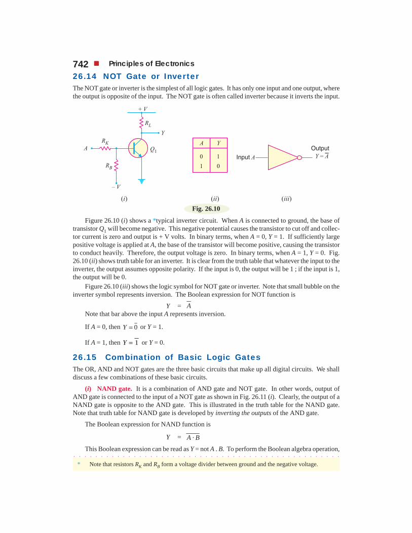
26.14 NOT Gate or InverterThe NOT gate or inverter is the simplest of all logic gates. It has only one input and one output, wherethe output is opposite of the input. The NOT gate is often called inverter because it inverts the input.
Fig. 26.10
Figure 26.10 (i) shows a *typical inverter circuit. When A is connected to ground, the base oftransistor Q1 will become negative. This negative potential causes the transistor to cut off and collec-tor current is zero and output is + V volts. In binary terms, when A = 0, Y = 1. If sufficiently largepositive voltage is applied at A, the base of the transistor will become positive, causing the transistorto conduct heavily. Therefore, the output voltage is zero. In binary terms, when A = 1, Y = 0. Fig.26.10 (ii) shows truth table for an inverter. It is clear from the truth table that whatever the input to theinverter, the output assumes opposite polarity. If the input is 0, the output will be 1 ; if the input is 1,the output will be 0.
Figure 26.10 (iii) shows the logic symbol for NOT gate or inverter. Note that small bubble on theinverter symbol represents inversion. The Boolean expression for NOT function is
Y = ANote that bar above the input A represents inversion.
If A = 0, then 0Y = or Y = 1.
If A = 1, then 1=Y or Y = 0.
26.15 Combination of Basic Logic GatesThe OR, AND and NOT gates are the three basic circuits that make up all digital circuits. We shalldiscuss a few combinations of these basic circuits.
(i) NAND gate. It is a combination of AND gate and NOT gate. In other words, output ofAND gate is connected to the input of a NOT gate as shown in Fig. 26.11 (i). Clearly, the output of aNAND gate is opposite to the AND gate. This is illustrated in the truth table for the NAND gate.Note that truth table for NAND gate is developed by inverting the outputs of the AND gate.
The Boolean expression for NAND function is
Y = ·A B
This Boolean expression can be read as Y = not A . B. To perform the Boolean algebra operation,
* Note that resistors RK and RB form a voltage divider between ground and the negative voltage.○ ○ ○ ○ ○ ○ ○ ○ ○ ○ ○ ○ ○ ○ ○ ○ ○ ○ ○ ○ ○ ○ ○ ○ ○ ○ ○ ○ ○ ○ ○ ○ ○ ○ ○ ○ ○ ○ ○ ○ ○ ○ ○ ○ ○ ○ ○ ○ ○

Digital Electronics 743first the inputs must be ANDed and then the inversion is performed. Note that output from a NANDgate is always 1 except when all of the inputs are 1. Fig. 26.11 (iii) shows the logic symbols for aNAND gate. The little bubble (small circle) on the right end of the symbol means to invert the AND.
Fig. 26.11
(ii) NOR gate. It is a combination of OR gate and NOT gate. In other words, output of OR gateis connected to the input of a NOT gate as shown in Fig. 26.12 (i). Note that output of OR gate isinverted to form NOR gate. This is illustrated in the truth table for NOR gate. It is clear that truthtable for NOR gate is developed by inverting the outputs of the OR gate.
Fig. 26.12The Boolean expression for NOR function is
Y = A B+
This Boolean expression can be read as Y = not A or B. To perform the Boolean algebra opera-tion, first the inputs must be ORed and then the inversion is performed. Note that output from a NORgate is high (1) only when all the inputs are low (0). If any of the inputs is high (1), the output is low(0). Fig. 26.12 (iii) shows the logic symbol for a NOR gate. The bubble (small circle) at the Y outputindicates inversion.
26.16 NAND Gate as a *Universal GateThe NAND gate is universal gate because its repeated use can produce other logic gates. The tablebelow shows how NAND gates can be connected to produce inverter (i.e., NOT gate), AND gate andOR gate.
* It may be noted that NOR gate is also a universal gate.○ ○ ○ ○ ○ ○ ○ ○ ○ ○ ○ ○ ○ ○ ○ ○ ○ ○ ○ ○ ○ ○ ○ ○ ○ ○ ○ ○ ○ ○ ○ ○ ○ ○ ○ ○ ○ ○ ○ ○ ○ ○ ○ ○ ○ ○ ○ ○ ○

744 Principles of Electronics
Fig. 26.13
(i) NOT gate from NAND gate. When two inputs of NAND gateare joined together so that it has one input, the resulting circuit is NOTgate. The truth table also shows this fact.
(ii) AND gate from NAND gates. Forthis purpose, we use two NAND gates in a manner as shown above. Theoutput of first NAND gate is given to the second NAND gate acting as in-verter (i.e., inputs of NAND gate joined). The resulting circuit is the ANDgate. The output Y′ of first NAND gate (AND gate followed by NOT gate) isinverted output of AND gate.The second NAND gate acting
as inverter further inverts it so that the final output Y isthat of AND gate. The truth table also shows this fact.
(iii) OR gate from NAND gates. For this purpose,we use three NAND gates in a manner as shown above.The first two NAND gates are operated as NOT gatesand their outputs are fed to the third. The resulting cir-cuit is OR gate. This fact is also indicated by the truth table.
26.17 Exclusive OR GateThe name exclusive OR gate is usually shortened to XOR gate. The XOR gate can be obtained byusing OR, AND and NOT gates as shown in Fig. 26.14 (i).
Fig. 26.14 (ii) shows the truth table for XOR gate. The table shows that the output is HIGH (1)if any but not all of the inputs are HIGH (1). This exclusive feature eliminates the similarity to the ORgate. The OR gate truth table is also given so that you can compare the OR gate truth table with XORgate truth table. The logic symbol for XOR gate is shown in Fig. 26.14 (iii). Note that the symbol issimilar to that of OR gate except for the additional curved line at the input side.
A B (= A) Y0 0 11 1 0
A B Y′ Y0 0 1 01 0 1 00 1 1 01 1 0 1
A B Y′ = A Y″ = B Y0 0 1 1 01 0 0 1 10 1 1 0 11 1 0 0 1

Digital Electronics 745
Fig. 26.14
The logic operations in the circuit are as under :
A B A B A B Y ′⋅ = ·A B Y ′′= Y = Y′ + Y″
0 0 1 1 0 0 0
1 0 0 1 0 1 1
0 1 1 0 1 0 1
1 1 0 0 0 0 0
Note that 0 ANDed with 1 is 0 and 1 ANDed with 1 is 1.
Example 26.11. Obtain the truth table for the circuit shown in Fig. 26.15 (i).
Solution. Figure 26.15 (ii) shows the truth table for the circuit. The truth table can be obtainedvery easily if the reader remembers the following simple Boolean operations :
Fig. 26.15
(i) 0 *ORed with 0 = 0 ; 1 ORed with 1 = 1 ; 1 ORed with 0 = 1
(ii) 0 **ANDed with 0 = 0 ; 0 ANDed with 1 = 0 ; 1 ANDed with 1 = 1Thus, when A = 0 and B = 0, then A ORed with B = 0 i.e., Y′ = 0. When Y′ (= 0) is ANDed with
A (= 0), the result is 0. Again when A = 1 and B = 0, then A ORed with B is 1 i.e., Y′ = 1. Now Y′(= 1) ANDed with A (= 1), the result is 1.
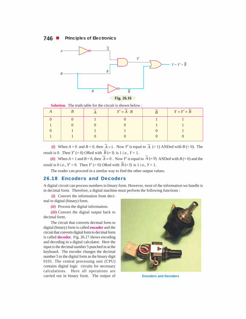
Example 26.12. Obtain the truth table for the circuit shown in Fig. 26.16.
* Note that A + B means A ORed with B.** Note that A . B means A ANDed with B.
○ ○ ○ ○ ○ ○ ○ ○ ○ ○ ○ ○ ○ ○ ○ ○ ○ ○ ○ ○ ○ ○ ○ ○ ○ ○ ○ ○ ○ ○ ○ ○ ○ ○ ○ ○ ○ ○ ○ ○ ○ ○ ○ ○ ○ ○ ○ ○ ○
746 Principles of Electronics
Fig. 26.16
Solution. The truth table for the circuit is shown below :A B A Y A B′ = ⋅ B Y Y B′= +
0 0 1 0 1 11 0 0 0 1 10 1 1 1 0 11 1 0 0 0 0
(i) When A = 0 and B = 0, then 1A = . Now Y′ is equal to A (= 1) ANDed with B (= 0). Theresult is 0. Then Y′ (= 0) ORed with ( 1)B = is 1 i.e., Y = 1.
(ii) When A = 1 and B = 0, then 0A = . Now Y′ is equal to ( 0)A = ANDed with B (= 0) and theresult is 0 i.e., Y′ = 0. Then Y′ (= 0) ORed with ( 1)B = is 1 i.e., Y = 1.
The reader can proceed in a similar way to find the other output values.
26.18 Encoders and DecodersA digital circuit can process numbers in binary form. However, most of the information we handle isin decimal form. Therefore, a digital machine must perform the following functions :
(i) Convert the information from deci-mal to digital (binary) form.
(ii) Process the digital information.(iii) Convert the digital output back to
decimal form.The circuit that converts decimal form to
digital (binary) form is called encoder and thecircuit that converts digital form to decimal formis called decoder. Fig. 26.17 shows encodingand decoding in a digital calculator. Here theinput is the decimal number 5 punched in at thekeyboard. The encoder changes the decimalnumber 5 to the digital form as the binary digit0101. The central processing unit (CPU)contains digital logic circuits for necessarycalculations. Here all operations arecarried out in binary form. The output of Encoders and Decoders
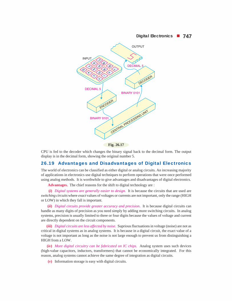
Digital Electronics 747
Fig. 26.17
CPU is fed to the decoder which changes the binary signal back to the decimal form. The outputdisplay is in the decimal form, showing the original number 5.
26.19 Advantages and Disadvantages of Digital ElectronicsThe world of electronics can be classified as either digital or analog circuits. An increasing majorityof applications in electronics use digital techniques to perform operations that were once performedusing analog methods. It is worthwhile to give advantages and disadvantages of digital electronics.
Advantages. The chief reasons for the shift to digital technology are :(i) Digital systems are generally easier to design. It is because the circuits that are used are
switching circuits where exact values of voltages or currents are not important, only the range (HIGHor LOW) in which they fall is important.
(ii) Digital circuits provide greater accuracy and precision. It is because digital circuits canhandle as many digits of precision as you need simply by adding more switching circuits. In analogsystems, precision is usually limited to three or four digits because the values of voltage and currentare directly dependent on the circuit components.
(iii) Digital circuits are less affected by noise. Suprious fluctuations in voltage (noise) are not ascritical in digital systems as in analog systems. It is because in a digital circuit, the exact value of avoltage is not important as long as the noise is not large enough to prevent us from distinguishing aHIGH from a LOW.
(iv) More digital circuitry can be fabricated on IC chips. Analog system uses such devices(high-value capacitors, inductors, transformers) that cannot be economically integrated. For thisreason, analog systems cannot achieve the same degree of integration as digital circuits.
(v) Information storage is easy with digital circuits.
748 Principles of Electronics
Disadvantages. (i) The real world is mainly analog. However, the digital circuits can handleonly digital signals. This necessitates encoders and decoders which increase the cost of the equip-ment.
(ii) There are situations where using only analog techniques is simpler and more economical.For example, the process of signal amplification is most easily accomplished using analog circuitry.
However, advantages of digital techniques outweigh the disadvantages. For this reason, we arefast switching to digital techniques.
26.20 Boolean AlgebraDigital circuits perform the binary arithmetic operations with binary digits 1 and 0. These opera-tions are called logic functions or logical operations. The algebra used to symbolically describelogic functions is called Boolean algebra. Boolean algebra is a set of rules and theorems by whichlogical operations can be expressed symbolically in equation form and be manipulated mathemati-cally. As with the ordinary algebra, the *letters of alphabet (e.g. A, B, C etc.) can be used torepresent the variables. Boolean algebra differs from ordinary algebra in that Boolean constantsand variables can have only two values ; 0 and 1. There are four connecting symbols used inBoolean algebra viz.
(i) equals sign (=) (ii) plus sign (+)(iii) multiply sign (·) (iv) bar (–)
(i) Equals sign (=). The equals sign in Boolean algebra refers to the standard mathematicalequality. In other words, the logical value on one side of the sign is identical to the logical value onthe other side of the sign. Suppose we are given two logical variables such that A = B. Then if A = 1,then B = 1 and if A = 0, then B = 0.
(ii) Plus sign (+). The plus sign in Boolean algebra refers to the logical OR operation. Thus,when the statement A + B = 1 appears in Boolean algebra, it means A ORed with B equals 1. Conse-quently, either A = 1 or B = 1 or both equal 1.
(iii) Multiply sign (·). The multiply sign in Boolean algebra refers to AND operation. Thus,when the statement A · B = 1 appears in Boolean algebra, it means A ANDed with B equals 1.Consequently, A = 1 and B = 1. The function A · B is often written as AB, omitting the dot forconvenience.
(iv) Bar sign (–). The bar sign in Boolean algebra refers to NOT operation. The NOT has theeffect of inverting (complementing) the logical value. Thus, if A = 1, then 0A = .
26.21 Boolean TheoremsWe now discuss the basic Boolean theorems that are useful in manipulating and simplifying Booleanexpressions. For convenience, we divide the theorems into two groups :
(i) Single variable theorems(ii) Multivariable theorems(i) Single variable theorems. These theorems refer to the condition when only one input to
the logic gate is variable. Table 26.1 gives single variable Boolean theorems.
* For example, A might represent a certain digital circuit input or output and at any time, we must haveeither A = 0 or A = 1.
○ ○ ○ ○ ○ ○ ○ ○ ○ ○ ○ ○ ○ ○ ○ ○ ○ ○ ○ ○ ○ ○ ○ ○ ○ ○ ○ ○ ○ ○ ○ ○ ○ ○ ○ ○ ○ ○ ○ ○ ○ ○ ○ ○ ○ ○ ○ ○ ○

Digital Electronics 749Table 26.1
Theorem 1 : A + 0 = ATheorem 2 : A · 1 = ATheorem 3 : 1A A+ =Theorem 4 : · 0A A =Theorem 5 : A + A = ATheorem 6 : A · A = ATheorem 7 : A + 1 = 1Theorem 8 : A · 0 = 0Theorem 9 : A A=
Theorem 1. (A + 0 = A). This theorem can be verifiedby ORing a variable A with a 0 and is illustrated in Fig. 26.18.Here one input to OR gate is always 0 and the other input Acan be a value 1 or 0. When A is at 1, the output is 1 which isequal to A. When A is at 0, the output is 0 which is also equalto A (= 0). Therefore, a variable ORed with 0 is equal to thevalue of the variable. This is easy to remember since 0 addedto anything does not effect the value of the variable, either inregular addition or OR addition.
Theorem 2. (A . 1 = A). This theorem can be verified by ANDing a variable A with a 1 and isillustrated in Fig. 26.19. Here one input to AND gate is always 1 and the other can be a value 1 or 0.
If A is 1, the output of the AND gate is 1 because both theinputs are now 1’s. If A is 0, the output of the AND gate is a0. Therefore, a variable ANDed with a 1 is equal to thevalue of the variable (A · 1 = A). This is easy to rememberbecause AND operation is just like ordinary multiplication.
Theorem 3.
( )1A A+ = . Thistheorem can be eas-
ily explained. If a variable A and its complement ( )A areORed, the result is always 1. If A is a 0, then 0 0 0 1 1+ = + = .If A is a 1, then 1 1 1 0 1+ = + = . Fig. 26.20 illustrates thistheorem.
Theorem 4. ( )· 0A A = . This theorem states that if avariable A is ANDed with its complement, the result is zero.This is readily apparent because either A or A will alwaysbe 0. Therefore, when one of the inputs to an AND gate is 0,the output is always 0. Fig. 26.21 illustrates this theorem.
Theorem 5. ( )+ =A A A . This theorem states that whena variable A is ORed with itself, the output is equal to the variable. Thus, if A is a 0, then 0 + 0 = 0 and
Fig. 26.19
Fig. 26.20
Fig. 26.18
Fig. 26.21

750 Principles of Electronics
if A is a 1, then 1 + 1 = 1. Fig. 26.22 illustrates this theorem.Theorem 6. (A · A = A). This theorem states that if a
variable A is ANDedwith itself, the resultis equal to the vari-able. For example, ifA = 0, then 0·0 = 0 and
if A = 1, then 1 · 1 = 1. For either case, the output of an ANDgate is equal to the value of the input variable A. Fig. 26.23illustrates this theorem.
Theorem 7. (A + 1 = 1). This theorem states that whena variable A is ORed with 1, the outuput is always equal to1. Fig. 26.24 illustrates this theorem. One input to an ORgate is always 1 and the other input A can be either 1 or 0.Now 1 on an input to OR gate produces 1 on the outputregardless of the value of the variable on the other input.
Theorem 8. (A · 0 = 0). This theorem states that vari-able A ANDed
with 0 always produces 0. Recall that any time one input toan AND gate is 0, the output is 0 regardless of the value of thevariable A on the other input. This theorem is illustrated inFig. 26.25.
Theorem 9. ( )A A= . This theo-rem states that if a variable A is comple-mented twice, the result is the variableitself. Starting with A and inverting(complementing) it once gives A . In-
verting it once more gives A — the original value. This theorem is illustrated in Fig. 26.26.Duality Principle. Before moving to multivariable theorems, this would be the right place to
mention an important property of Boolean algebra called duality principle. It is stated below :The duality principle states that a Boolean expression remains valid if operators OR and AND
are interchanged and 1’s and 0’s in the expression are also interchanged.In order to understand this principle, consider the Boolean Theorem 1 viz.
A + 0 = AAccording to duality principle, this Boolean expression remains valid if OR function is replaced
by AND function and 0 by 1. In that case, the Boolean expression becomes :A · 1 = A
Note that this is Boolean Theorem No. 2. Therefore, Boolean Theorem 2 is dual of BooleanTheorem 1 and vice-versa. Applying duality principle, Theorem 4 is dual of Theorem 3 and vice-versa, Theorem 6 is dual of Theorem 5 and vice-versa, Theorem 8 is dual of Theorem 7 and vice-versa. To apply duality principle to a Boolean expression, we simply interchange OR and ANDoperator and replace 1’s by 0’s and 0’s by 1’s.
(ii) Multivariable theorems. These theorems refer to the condition when more than one inputto the logic gate are variable. Table 26.2 gives multivariable Boolean theorems.
Fig. 26.24
Fig. 26.25
Fig. 26.26
Fig. 26.22
Fig. 26.23

Digital Electronics 751
}}
}
Table 26.2
Theorem 10 : A + B = B + ATheorem 11 : A · B = B · ATheorem 12 : A + (B + C) = (A + B) + CTheorem 13 : A · (B · C) = (A · B) · CTheorem 14 : A · (B + C) = A · B + A · CTheorem 15 : (A + B) · (C + D) = A · C + B · C + A · D + B · DTheorem 16 : A + A · B = ATheorem 17 : ( )+ = ⋅A B A BTheorem 18 : ( ) = +⋅ A BA B
The following points may be noted about these theorems :(a) Theorems 10 and 11 obey commutative law. This law states that the order in which the
variables are ORed or ANDed makes no difference.
Fig. 26.27
Fig. 26.28
Figure 26.27 illustrates the commutative law as applied to the OR gate while Fig. 26.28 illus-trates the commutative law as applied to an AND gate.
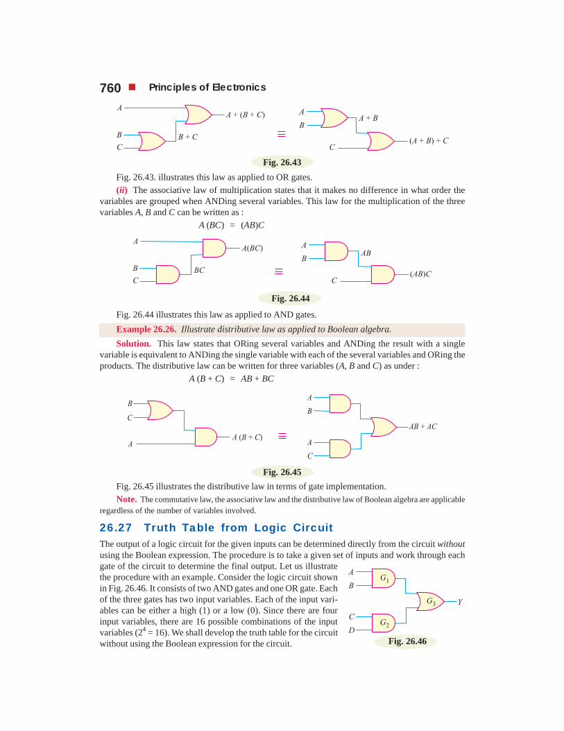
(b) Theorems 12 and 13 obey associative law. This law states that in the ORing or ANDing ofseveral variables, the result is the same regardless of the grouping of the variables.
Fig. 26.29
Fig. 26.30
Figure 26.29 illustrates the associative law as applied to the OR gate, while Fig. 26.30 illustratesthe associative law as applied to an AND gate.
(c) Theorems 14 and 15 obey distributive law. This law states that a Boolean expression canbe expanded by multiplying term-by-term just the same as in ordinary algebra.
Commutative Law
Associative Law
Distributive Law
De Morgan’s Theorems⎫⎪⎬⎪⎭

752 Principles of Electronics
Fig. 26.31
Fig. 26.31 illustrates the distributive law in terms of gate implementation.(d) We will prove Theorem 16 by factoring and using Theorems 2, 7, 10 and 14.
A + A · B = A · 1 + A · B ...Theorem 2= A · (1 + B) ...Theorem 14= A · (B + 1) ...Theorem 10= A · 1 ...Theorem 7= A ...Theorem 2
(e) Theorems 17 and 18 are the two most important theorems of Boolean algebra and werecontributed by the great mathematician named De Morgan. Therefore, these theorems are called DeMorgan’s theorems.
26.22 De Morgan’s TheoremsDe Morgan’s theorems are extremely useful in simplifying expressions in which a product or sum ofvariables is inverted. The two theorems are :
(i) ( ) = ⋅+ A BA B
(ii) ( ). = +A BA B(i) The first De Morgan’s theorem may be stated as under :When the OR sum of two variables is inverted, this is equal to inverting each variable
individually and then ANDing these inverted variables i.e.,
( )+A B = A B⋅In this expression, A and B are the two variables. The L.H.S. is the complement of the OR sum
of the two variables. The R.H.S. is the AND product of individual inverted variables.(ii) The second De Morgan’s theorem may be stated as under :When the AND product of two variables is inverted, this is equal to inverting each variable
individually and then ORing them i.e.,
( )⋅A B = A B+In this expression, A and B are the two variables. The L.H.S. is the complement of the AND
product of the two variables. The R.H.S. is the OR sum of the individual inverted variables.
26.23 Operator PrecedenceThe operator precedence for evaluating Boolean expression is (i) parenthesis (ii) NOT (iii) AND and(iv) OR. In other words, the expression inside the parenthesis must be evaluated before all otheroperations. The next operation that holds precedence is the complement, then follows the AND andfinally the OR. For example, consider the Boolean expression : . ( )A B C D+ +

Digital Electronics 753The sequence of operations will be :(i) The expression inside the parenthesis (i.e. C + D) will be evaluated first.
(ii) Then B will be evaluated.(iii) Then the results of the two (i.e. B and C + D) will be ANDed.(iv) Finally, the result of the product will be ORed with A.
Example 26.13. Using Boolean algebraic techniques, simplify the following expression :Y = · · · · · · · · · · · ·A B C D A B C D A B C D A B C D+ + +
Solution. Y = · · · · · · · · · · · ·A B C D A B C D A B C D A B C D+ + + ...(i)Step 1 : Take out the common factors as below :
Y = ( ) ( )B C D A A B C D A A+ + +
Step 2 : Apply Theorem 3 ( 1)A A+ = :
Y = B C D B C D+Step 3 : Again factorise :
Y = ( )B D C C+
Step 4 : Apply Theorem 3 ( 1)C C+ = :
Y = ·1B D BD=This is the simplified form of exp. (i).Example 26.14. Using Boolean techniques, simplify the following expression :
Y = AB + A (B + C) + B (B + C)Solution. Y = AB + A (B + C) + B (B + C) ...(i)Step 1 : Apply Theorem 14 (distributive law) to second and third terms:
Y = AB + AB + AC + BB + BCStep 2 : Apply Theorem 6 (B · B = B) :
Y = AB + AB + AC + B + BCStep 3 : Apply Theorem 5 (AB + AB = AB) :
Y = AB + AC + B + BCStep 4 : Factor B out of last 2 terms :
Y = AB + AC + B (1 + C)Step 5 : Apply commutative law and Theorem 7 (1 + C = C + 1 = 1) :
Y = AB + AC + B · 1Step 6 : Apply Theorem 2 (B · 1 = B) :
Y = AB + AC + BStep 7 : Factor B out of first and third terms :
Y = B (A + 1) + ACStep 8 : Apply Theorem 7 (A + 1 = 1) :
Y = B · 1 + ACStep 9 : Apply Theorem 2 (B · 1 = B) :
Y = B + ACThis is the simplified form of exp. (i).

754 Principles of Electronics
Example 26.15. Simplify the following Boolean expressions to a minimum number of literals :(i) Y = A A B+ (ii) Y = AB AC BC+ +
Solution. (i) Y = A A B+
= A AB AB+ + [ä A = A + AB from Theorem 16]( )A B A A= + +
= A + B [ä A A+ = 1 from Theorem 3]∴ Y = A + B(ii) Y = AB AC BC+ +
= · ( )AB AC BC A A+ + +
= AB AC ABC ABC+ + +
= AB (1 + C) + AC (1 + B)= AB + AC
∴ Y = AB + ACExample 26.16. Determine output expression for the circuit shown below and simplify it using
De Morgan’s theorem.
Fig. 26.32
Solution. The output expression for the circuit shown above is :
Y = [( ) · · ]A B C D+Using De Morgan’s theorem :
Y = (A + B) + C D+
∴ Y = A + B + C D+Example 26.17. Find the complement of the expressions given below :
(i) Y = ABC ABC+
(ii) Y = ( )A BC BC+ +
Solution. (i) Y = ABC ABC+
Y = ( )ABC ABC+Applying De Morgan’s theorem :
Y = ( ) · ( )ABC ABCAgain applying De Morgan’s theorem to the each expression inside the brackets :
Y = ( ) · ( )A B C A B C+ + + +(ii) Y = ( )A BC BC+

Digital Electronics 755
Y = ( )A BC BC+Applying De Morgan’s theorem :
Y = ( )A BC BC+ +Again applying De Morgan’s theorem to the expression inside the bracket :
Y = ( ) · ( )+A BC BCApplying De Morgan’s theorem for the third time we get :
Y = ( ) · ( )A B C B C+ + +
or Y = A BC BC+ +Example 26.18. Simplify the following Boolean expressions :(i) Y = (A + B + C) · (A + B)
(ii) Y = AB + ABC + ABC
(iii) Y = 1 ( · )A B C BC B C ABC AC+ + + + +
(iv) Y = ( ) ( )A B C B C+ + + +
Solution. (i) Y = (A + B + C) · (A + B)= A · A + A · B + B · A + B · B + C · A + C · B
Using A · A = A, we get,Y = A + AB + AB + B + AC + BC
= A + AB + B + AC + BC [ä AB + AB = AB]= A + B + AC + BC [ä A + AB = A]= A (1 + C) + B (1 + C)= A · 1 + B · 1 [ä 1 + C = 1]
∴ Y = A + B(ii) Y = AB + ABC + ABC
= AB + AB ( )C C+
= AB + AB [ä C C+ = 1]∴ Y = AB(iii) Y = 1 ( · )+ + + + +A B C BC B C ABC AC
Using 1 + A = 1, we get,
Y = 1 + ABC + AC [ä 1 ( )+ + +A BC BC BC = 1]= 1 + AC
∴ Y = 1Thus, because of the first term Y reduces to 1. Therefore, any Boolean expression ORed with 1,
results in 1.
(iv) Y = ( ) ( )A B C B C+ + + +Applying De Morgan’s theorem :
Y = ( ) · ( )A B C B C+ + +Again applying De Morgan’s theorem :
Y = ( · · ) · ( · )A B C B C = 0 [ä · 0, · 0B B C C= = ]

756 Principles of Electronics
Example 26.19. Simplify the following Boolean expression :
Y = A B D A B D+
Solution. Y = A B D A B D+
Factoring out the common variables A B (using Theorem 14), we get ,
Y = ( )A B D D+
Using Theorem 3, D D+ = 1.
∴ Y = ·1A BUsing Theorem 2, we get,
Y = A B
Example 26.20. Simplify the following Boolean expression :Y = ( ) ( )A B A B+ +
Solution. Y = ( ) ( )A B A B+ +The expression can be expanded by multiplying out the terms [Theorem 15].
Y = · · · ·A A A B B A B B+ + +
Using Theorem 4, ·A A = 0. Also B . B = B [Theorem 6].
∴ Y = 0 · ·A B B A B+ + +
= ·A B A B B+ +Factoring out the variable B [Theorem 14], we have,
Y = ( 1)B A A+ +Using Theorem 7, A + 1 = 1.
∴ Y = ( 1)B A +
Again using Theorem 7, 1A + = 1.
∴ Y = B · 1Finally, using Theorem 2, we have,
Y = B
26.24 Combinational Logic CircuitsWe can combine two or more logic gates to form a logic circuit or digital circuit. When the resultinglogic or digital circuit has no feedback and no memory, it is often called combinational logic circuit.
A logic circuit consisting of two or more logic gates that has no feedback and no memory iscalled a combinational logic circuit.
A combinational logic circuit is constructed using OR, AND and NOT gates. Therefore, the basicbuilding block for combinational circuits is the logic gate. Since a combinational logic circuit has nofeedback and no memory, its output depends only on the current value of its inputs.
26.25 Boolean Expressions for Combinational Logic CircuitsA combinational logic circuit (or digital circuit) often consists of several different logic gates, inter-connected in such a way as to perform a specific logic function. By using the laws, theorems andtechniques of Boolean algebra, we can find the Boolean expression for any combinational logiccircuit. Let us find Boolean expression for some logic circuits.

Digital Electronics 757(i) Fig. 26.33 shows a logic circuit. It
consists of two AND gates and one OR gate.Each of the three gates has two input variables.Because gate G1 is an AND gate and its twoinputs are A and B, its output is AB. The gateG2 is also an AND gate and its two inputs areC and D so that its output is CD. The gate G3is an OR gate so that its output is the ORing ofAB and CD, producing AB + CD. Therefore,the Boolean expression for the output of thislogic circuit is
Y = AB + CD(ii) Fig. 26.34 shows a logic circuit consisting of two AND gates and one OR gate. There are
four (A, B, C and D) input variables.
Fig. 26.34
The variable C is ANDed with D and its output is CD. Then CD is ORed with B, giving an output(B + CD). This sum is then ANDed with A, resulting in the following Boolean expression :
Y = A (B + CD)(iii) Fig. 26.35 shows a logic circuit consisting of three AND gates and one OR gate. There are
six input variables viz. A, B, C, D, E and F.
Fig. 26.35
The variables A and B are ANDed to produce AB, B, C and D are ANDed to produce BCD and E andF are ANDed to produce EF. The input to OR gate is AB, BCD and EF so the output of this gate is theORing of the inputs i.e.
Y = AB + BCD + EF
26.26 AND and OR Operations in Boolean ExpressionIt is very important to interpret AND and OR operations in the Boolean expression. Sometimes, theremay be confusion as to which operation (AND or OR) in a Boolean expression is to be performed
Fig. 26.33

758 Principles of Electronics
* Recall that it indicates A ANDed with B and can be expressed as A⋅B or AB.○ ○ ○ ○ ○ ○ ○ ○ ○ ○ ○ ○ ○ ○ ○ ○ ○ ○ ○ ○ ○ ○ ○ ○ ○ ○ ○ ○ ○ ○ ○ ○ ○ ○ ○ ○ ○ ○ ○ ○ ○ ○ ○ ○ ○ ○ ○ ○ ○
first. For example, the Boolean expression *A ⋅ B + C can be interpreted in two different ways viz.(i) A ⋅ B is ORed with C or (ii) A is ANDed with the term B + CIn order to avoid this confusion, it will be understood that if Boolean expression contains both
AND and OR operations, the AND operations are performed first unless there are brackets in theexpression in which case the operation inside the brackets is to be performed first. This is the samerule that is used in ordinary algebra to determine the order of operations. Let us illustrate this impor-tant point with examples.
(i) Consider the Boolean expression:Y = A ⋅ B + C. Since there are no brackets in thisexpression, AND operation is to be performedfirst. In other words, first A and B are ANDed toproduce A ⋅ B and then A ⋅ B is ORed with C togive the final function: Y = A ⋅ B + C. The logiccircuit representing this Boolean expression is shown in Fig. 26.36.
(ii) Consider the Boolean expression: Y = (A + B) ⋅ C. Since A + B is in the bracket, theOR operation is to be performed first. Inother words, A is ORed with B to give (A + B)and then (A + B) is ANDed with C to produce Y= (A + B) ⋅ C. The logic circuit representingthis Boolean expression is shown in Fig. 26.37.
Example 26.21. Write the Boolean expres-sion for the digital circuit shown in Fig. 26.38.
Solution. The output of G2 is A + B . Thisoutput of G2 is NANDed with C to yield Y =
( )+A B C . Note that bracket around (A + B ) isrequired otherwise the expression may be inter-
preted that A is NORed with B C.
Example 26.22. Write the Boolean expression for the logic circuit (digital circuit) shown inFig. 26.39.
Fig. 26.39
Solution. There are two AND gates (viz. G1 and G3) and one OR gate (G2). Also the circuit hastwo inverters. The input A is fed to G1 through the inverter. Therefore, A , B and C are ANDed by G1
to produce an output of A BC. The input A is ORed with D by G2 to produce an output of (A + D). Theinputs ABC and ( )A D+ to G3 are ANDed to produce the final output :
Y = ( )+ABC A D
Fig. 26.36
Fig. 26.37
Fig. 26.38

Digital Electronics 759Example 26.23. Write the Boolean expression for the digital circuit shown in Fig. 26.40.
Fig. 26.40
Solution. The output of G1 is A + B. Then (A + B) and C are ANDed to produce an output of
(A + B) C. It is easy to see ( )A B C+ and D are ORed by G3 to produce an output of D + ( )A B C+ ⋅ .
Finally, D + ( )A B C+ ⋅ and E are ANDed by G4 to produce the final output Y given by ;
Y = [D + ( )+A B C ] ⋅ ⋅ ⋅ ⋅ ⋅ E
Example 26.24. Illustrate the commutative law of (i) addition and (ii) multiplication of twovariables.
Solution.(i) The commutative law of addition states that the order in which the variables are ORed
makes no difference. This law for the addition of two variables A and B can be written as :A + B = B + A
Fig. 26.41
Fig. 26.41 illustrates the commutative law as applied to the OR gate.(ii) The commutative law of multiplication states that the order in which the variables are ANDed
makes no difference. This law for the multiplication of two variables A and B can be written as :AB = BA
Fig. 26.42
Fig. 26.42 illustrates the commutative law as applied to the AND gate.Example 26.25. Illustrate associative law of (i) addition and (ii) multiplication as applied to
Boolean algebra.Solution.(i) The associative law of addition states that in the ORing of several variables, the result is the
same regardless of the grouping of the variables. This law for the addition of the three variables A, Band C can be written as:
A + (B + C) = (A + B) + C
760 Principles of Electronics
Fig. 26.43Fig. 26.43. illustrates this law as applied to OR gates.(ii) The associative law of multiplication states that it makes no difference in what order the
variables are grouped when ANDing several variables. This law for the multiplication of the threevariables A, B and C can be written as :
A (BC) = (AB)C
Fig. 26.44
Fig. 26.44 illustrates this law as applied to AND gates.Example 26.26. Illustrate distributive law as applied to Boolean algebra.Solution. This law states that ORing several variables and ANDing the result with a single
variable is equivalent to ANDing the single variable with each of the several variables and ORing theproducts. The distributive law can be written for three variables (A, B and C) as under :
A (B + C) = AB + BC
Fig. 26.45Fig. 26.45 illustrates the distributive law in terms of gate implementation.Note. The commutative law, the associative law and the distributive law of Boolean algebra are applicable
regardless of the number of variables involved.
26.27 Truth Table from Logic CircuitThe output of a logic circuit for the given inputs can be determined directly from the circuit withoutusing the Boolean expression. The procedure is to take a given set of inputs and work through eachgate of the circuit to determine the final output. Let us illustratethe procedure with an example. Consider the logic circuit shownin Fig. 26.46. It consists of two AND gates and one OR gate. Eachof the three gates has two input variables. Each of the input vari-ables can be either a high (1) or a low (0). Since there are fourinput variables, there are 16 possible combinations of the inputvariables (24 = 16). We shall develop the truth table for the circuitwithout using the Boolean expression for the circuit. Fig. 26.46

Digital Electronics 761First, suppose each input is low (i.e. A = 0, B = 0, C = 0 and D = 0). Under this condition, we shall
examine the output of each gate in the circuit to arrive at the final output Y. If the inputs to gate G1 arelow (0), the output of G1 is low (0). Also the output of G2 is low (0) because both inputs are low (0).The two low inputs to G3 also make its output low (0). Therefore, the output of the logic circuit is lowwhen all the inputs are low as shown in the truth table. Similarly, we can find the output of the circuitfor the remaining 15 input combinations.
Truth TableY = AB + CD
Inputs G1 Output G2 Output G3 OutputA B C D (AB) (CD) Y0 0 0 0 0 0 00 0 0 1 0 0 00 0 1 0 0 0 00 0 1 1 0 1 10 1 0 0 0 0 00 1 0 1 0 0 00 1 1 0 0 0 00 1 1 1 0 1 11 0 0 0 0 0 01 0 0 1 0 0 01 0 1 0 0 0 01 0 1 1 0 1 11 1 0 0 1 0 11 1 0 1 1 0 11 1 1 0 1 0 11 1 1 1 1 1 1
Note. We can also construct the truth table by devel-oping the Boolean expression from the logic circuit. Thelogic circuit shown above (See Fig. 26.46) is redrawn asshown in Fig. 26.47. The Boolean expression for this logiccircuit is
Y = AB + CDNow simply put in the values for each combina-
tion of inputs and use the Boolean rules and laws todetermine the final output Y. For example, when A = 1,B = 1, C = 1 and D = 0, the final output is
Y = AB + CD= 1.1 + 1.0= 1 + 0= 1
Similary, we can find Y for the remaining 15 input combinations to get the truth table shown above.
Fig. 26.47
762 Principles of Electronics
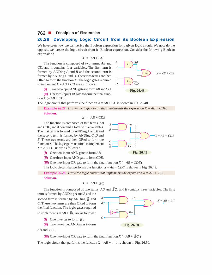
26.28 Developing Logic Circuit from its Boolean ExpressionWe have seen how we can derive the Boolean expression for a given logic circuit. We now do theopposite i.e. create the logic circuit from its Boolean expression. Consider the following Booleanexpression :
X = AB + CDThe function is composed of two terms, AB and
CD, and it contains four variables. The first term isformed by ANDing A and B and the second term isformed by ANDing C and D. These two terms are thenORed to form the function X. The logic gates requiredto implement X = AB + CD are as follows :
(i) Two two-input AND gates to form AB and CD.(ii) One two-input OR gate to form the final func-
tion X (= AB + CD).The logic circuit that performs the function X = AB + CD is shown in Fig. 26.48.
Example 26.27. Drawn the logic circuit that implements the expression X = AB + CDE.Solution.
X = AB + CDEThe function is composed of two terms, AB
and CDE, and it contains a total of five variables.The first term is formed by ANDing A and B andthe second term is formed by ANDing C, D andE. These two terms are then ORed to form thefunction X. The logic gates required to implementX = AB + CDE are as follows :
(i) One two-input AND gate to form AB.(ii) One three-input AND gate to form CDE.(iii) One two-input OR gate to form the final function X (= AB + CDE).The logic circuit that performs the function X = AB + CDE is shown in Fig. 26.49.Example 26.28. Draw the logic circuit that implements the expression X = AB + BC.Solution.
X = AB + BC
The function is composed of two terms, AB and BC , and it contains three variables. The firstterm is formed by ANDing A and B and thesecond term is formed by ANDing B andC. These two terms are then ORed to formthe final function. The logic gates requiredto implement X = AB + BC are as follows :
(i) One inverter to form B .(ii) Two two-input AND gates to form
AB and BC .
(iii) One two-input OR gate to form the final function X (= AB + BC ).
The logic circuit that performs the function X = AB + BC is shown in Fig. 26.50.
Fig. 26.48
Fig. 26.49
Fig. 26.50

Digital Electronics 763Example 26.29. Draw the logic circuit that implements the expression X = AB ( CD + EF).Solution.
X = AB ( CD + EF)A breakdown of this equation shows that the term AB and the term CD + EF are ANDed. The
term AB is formed by ANDing the variables A and B. The term CD + EF is formed first by ANDingC and D , ANDing E and F and then ORing these two terms. The logic gates required to implementX = AB ( CD + EF) are as follows :
(i) One inverter to form D .
(ii) Two two-input AND gates to form CD and EF.
(iii) One two-input OR gate to form CD + EF.(iv) One two-input AND gate to form AB.
(v) One two-input AND gate to form X [=AB ( CD + EF)].
Fig. 26.51
The logic circuit that forms the function X = AB (CD + EF) is shown in Fig. 26.51.
26.29 Sum-of-Products FormThe sum-of-products form of a Boolean expression consists of two or more AND terms (i.e. prod-ucts) that are ORed together. For example, AB + CD is a sum-of-products expression. Here ANDterms AB and CD are ORed (added). Other examples of this form are :
(i) ABC ABC+
(ii) ABC DEF AEF+ +
(iii) A BCD EFG+ +The sum-of-products is a very useful formof a Boolean expression due to the straight-forward manner is which it can be imple-mented in logic gates. For example, Fig.26.52 shows the logic circuit that results ina sum-of-products form. It has simply twosteps: ANDing and then ORing. Therefore, Fig. 26.52
764 Principles of Electronics
this form is always only a two-level gate network i.e. the maximum number of gates through which asignal must pass in going form input to output is two (excluding inversions, but these can also beworked in).
26.30 Simplification of Boolean ExpressionsThe form of Boolean expression determines how many and which types of logic gates are needed aswell as how they are connected together. The more complicated the Boolean expression, the morecomplex the logic circuit will be. It is, therefore, desirable to simplify an expression as much aspossible to get the simplest logic circuit. Note that the new expression can be used to implement alogic circuit that is equivalent to the original logic circuit but contains fewer gates and connections.While simplifying a Boolean expression, the following two steps may be very helpful:
(i) Put the original expression into the sum-of-products form by the repeated use of rules, theo-rems and techniques of Boolean algebra.
(ii) Once it is in this form, the product terms are checked for common factors and factoring isperformed wherever possible.
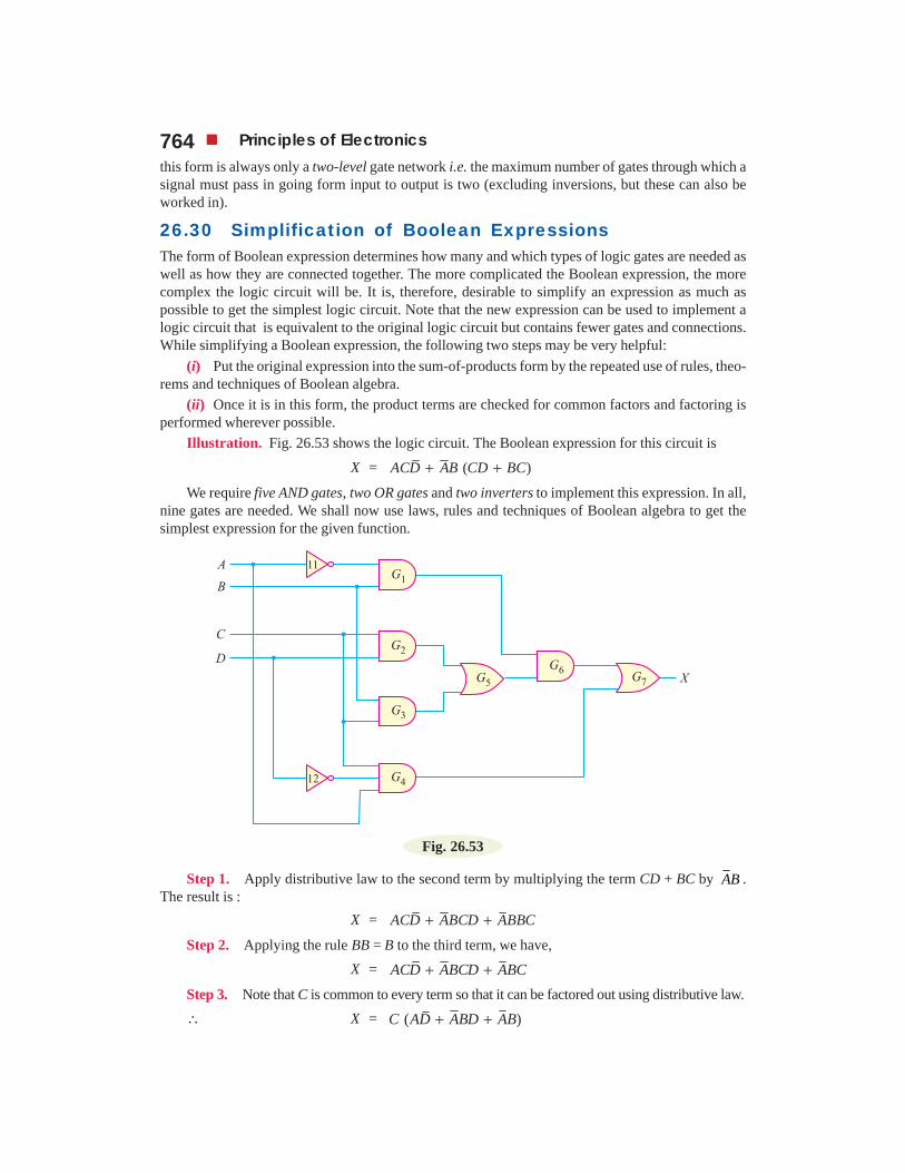
Illustration. Fig. 26.53 shows the logic circuit. The Boolean expression for this circuit is
X = ( )ACD AB CD BC+ +
We require five AND gates, two OR gates and two inverters to implement this expression. In all,nine gates are needed. We shall now use laws, rules and techniques of Boolean algebra to get thesimplest expression for the given function.
Fig. 26.53
Step 1. Apply distributive law to the second term by multiplying the term CD + BC by AB .The result is :
X = ACD ABCD ABBC+ +
Step 2. Applying the rule BB = B to the third term, we have,X = ACD ABCD ABC+ +
Step 3. Note that C is common to every term so that it can be factored out using distributive law.∴ X = ( )C AD ABD AB+ +

Digital Electronics 765Step 4. We see that the term AB appears in the last two terms within the bracket and can be
factored out of those two terms.∴ X = [ ( 1)]C AD AB D+ +
Since D + 1 = 1, X = ( )C AD AB+It appears that this equation cannot be simplified any further, but is can be written in a slightly
different way by applying the distributive law (this results in the sum-of-products form):
X = ACD ABC+
Fig. 26.54
Implementing this equation (i.e. X = ACD ABC+ ) into the logic circuit, it only requires twothree-input AND gates, two inverters and one two-input OR gate as shown in Fig. 26.54. Note thatthis minimised circuit is equivalent to the original circuit of Fig. 26.53 but only requires five gates(instead of nine).
Example 26.30. Simplify the expression :
X = ABC ABC ABC ABC+ + +Solution.
X = ABC ABC ABC ABC+ + +
Step 1. Note that the first two terms have BC as common factors while the last two terms haveAB as common factors.
∴ X = ( ) ( )BC A A AB C C+ + +
Step 2. A A+ = 1 and C C+ = 1 so that :
X = 1 1BC AB⋅ + ⋅
Step 3. Since 1BC ⋅ = BC and AB⋅1 = AB so that :
X = AB + BCNote that not only is the Boolean expression simplified, but so is the resultant logic circuit.Example 26.31. Simplify the expression :
X = AB + A (B + C) + B (B + C)Solution.
X = AB + A (B + C) + B (B + C)Step 1. Applying distributive law to the second and third terms, we have,
X = AB + AB + AC + BB + BC

766 Principles of Electronics
○ ○ ○ ○ ○ ○ ○ ○ ○ ○ ○ ○ ○ ○ ○ ○ ○ ○ ○ ○ ○ ○ ○ ○ ○ ○ ○ ○ ○ ○ ○ ○ ○ ○ ○ ○ ○ ○ ○ ○ ○ ○ ○ ○ ○ ○ ○ ○ ○
Step 2. Now BB = B and AB + AB = AB so that :X = AB + AC + B + BC
Step 3. B + BC = B(1 + C) = B⋅1 = B∴ X = AB + AC + BStep 4. Factoring B out, we have,
X = B(A + 1) + ACStep 5. A + 1 = 1 so that B( A + 1) = B⋅1 = B.∴ X = B + ACThe original expression is simplified as far as it can go. Once you get acquainted with Boolean
simplification techniques, you can combine many individual steps.Example 26.32. Simplify the circuit of Fig. 26.55 (i).
Fig. 26.55Solution. The Boolean expression for the circuit shown in Fig. 26.55 (i) is
X = ( ) ( )A B A B+ +Step 1. Multiplying out to get the sum-of-products form, we have,
X = AA AB BA BB+ + +
Step 2. Now AA = 0 and BB = 0 so that :X = AB AB+
This expression is implemented in Fig. 26.55 (ii). If you compare the circuit with the originalcircuit, you see that both circuits contain the same number of gates and connections. Therefore, thesimplification process has not produced a simpler circuit but it has produced an alternative circuit.
26.31 Binary AdditionThe addition of two binary numbers is performed in exactly the same manner as the addition of
decimal numbers. In fact, binary addition is simpler, because we have only two digits (0 and 1). Whenadding binary numbers, the following rules apply :
0 + 0 = 01 + 0 = 11 + 1 = 10 = 0 + carry of 1 into next position
1 + 1 + 1 = 11 = 1 + carry of 1 into next positionIt is not necessary to consider the addition of more than two binary numbers at a time. It is
because the circuitry that actually performs the addition in a digital system can handle only twonumbers at a time. When more than two numbers are to be added, the first two are added together andthen their sum is added to the third number and so on.
Examples. Let us illustrate binary addition with two examples.
* This is the alternate symbol for the inverter.

Digital Electronics 767(i) Let us add the following two binary numbers :
1 0 1+ 0 1 0
1 1 1
The addition is done column by column starting at the right as it is in the decimal number system.For the first column, 1 + 0 = 1 and for the second column, 0 + 1 = 1. For the third or last column, 1 +0 = 1. This produces a sum of 111.
(ii) Let us now add the following two binary numbers :1 0 1 1 1
+ 1 0 0 1 01 0 1 0 0 1
For the first column, 1 + 0 = 1. In the second column, we have, 1 + 1 = 10 = 0 with a carry of 1.For the third column, we have, 1 + 0 + carry of 1 = 1 + 1 = 10 = 0 with a carry of 1. For the fourthcolumn, 1 + 0 + 0 = 1 + 0 = 1. For the fifth column, we have 1 + 1 = 10 = 0 with a carry of 1. Thisproduces a sum of 101001.
Binary addition is the most important arithmetic operation in digital systems. It is because theoperations of subtraction, multiplication and division as they are performed in most modern digitalcomputers and calculators actually use only addition as their basic operation. To be an intelligentworker on digital equipment, you must master binary addition.
26.32 Electronic AddersA logic circuit that performs the function of binary addition is called electronic adder or adder. Theadder circuit consists of properly connected logic gates. There are usually two forms of the adder incommon applications viz. (i) half adder (ii) full adder.
(i) Half Adder (HA). A logic circuit that can add two binary bits is called a half adder (HA).Fig. 26.56 (i) shows the block symbol for the half adder. The adder circuit would need two inputs andtwo outputs. The two inputs are for the two digits to be added, either 0 or 1. One output terminal is forthe sum of the two inputs and the other output is for the carry, if necessary. Fig. 26.56 (ii) shows theaddition table of the adder and can be thought of as a truth table. The numbers being added are on theinput side of the table. The truth table has two output columns, one column for the sum and onecolumn for the carry. The sum column is labeled with summation symbol Σ. The carry column islabeled with Co. The Co stands for carry output or carry out. Thus the half adder circuit has two inputs(A, B) and two outputs (Σ, Co).
Fig. 26.56The half adder would behave according to the truth table shown in Fig. 26.56 (ii). Take a careful
look at the truth table. The output columns (sum and carry) can be produced by using two gates asunder :
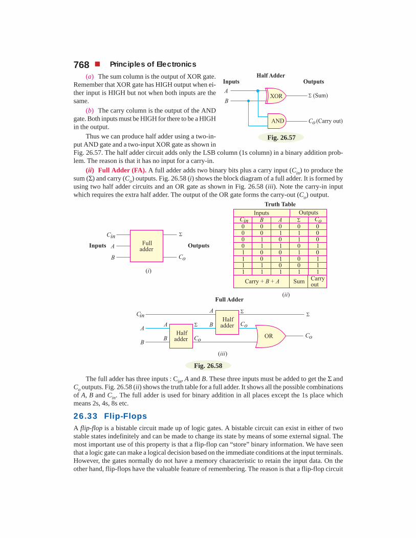
768 Principles of Electronics
(a) The sum column is the output of XOR gate.Remember that XOR gate has HIGH output when ei-ther input is HIGH but not when both inputs are thesame.
(b) The carry column is the output of the ANDgate. Both inputs must be HIGH for there to be a HIGHin the output.
Thus we can produce half adder using a two-in-put AND gate and a two-input XOR gate as shown inFig. 26.57. The half adder circuit adds only the LSB column (1s column) in a binary addition prob-lem. The reason is that it has no input for a carry-in.
(ii) Full Adder (FA). A full adder adds two binary bits plus a carry input (Cin) to produce thesum (Σ) and carry (Co) outputs. Fig. 26.58 (i) shows the block diagram of a full adder. It is formed byusing two half adder circuits and an OR gate as shown in Fig. 26.58 (iii). Note the carry-in inputwhich requires the extra half adder. The output of the OR gate forms the carry-out (Co) output.
Fig. 26.58
The full adder has three inputs : Cin, A and B. These three inputs must be added to get the Σ andCo outputs. Fig. 26.58 (ii) shows the truth table for a full adder. It shows all the possible combinationsof A, B and Cin. The full adder is used for binary addition in all places except the 1s place whichmeans 2s, 4s, 8s etc.
26.33 Flip-FlopsA flip-flop is a bistable circuit made up of logic gates. A bistable circuit can exist in either of twostable states indefinitely and can be made to change its state by means of some external signal. Themost important use of this property is that a flip-flop can “store” binary information. We have seenthat a logic gate can make a logical decision based on the immediate conditions at the input terminals.However, the gates normally do not have a memory characteristic to retain the input data. On theother hand, flip-flops have the valuable feature of remembering. The reason is that a flip-flop circuit
Fig. 26.57

Digital Electronics 769
○ ○ ○ ○ ○ ○ ○ ○ ○ ○ ○ ○ ○ ○ ○ ○ ○ ○ ○ ○ ○ ○ ○ ○ ○ ○ ○ ○ ○ ○ ○ ○ ○ ○ ○ ○ ○ ○ ○ ○ ○ ○ ○ ○ ○ ○ ○ ○ ○
is bistable. Because the flip-flop’s output remains at a 0 or 1 depending on the last input signal, theflip-flop can be said to “remember”. Another name for the flip-flop is bistable multivibrator. We shalldiscuss two important types of flip-flops viz. (i) R–S flip-flop and (ii) J–K flip-flop.
(i) R–S Flip-Flop. The *R–S type is the basic flip-flop logic circuit. Fig. 26.59 (i) shows thelogic symbol for an R–S flip flop. It has two inputs called set (S) and reset (R). The two outputs are
labeled as Q and Q . In flip-flops, the outputs are always opposite or complementary. In other words,
if output Q = 1, then output Q = 0 and so on. Note the small bubbles for inversion at the S and R inputterminals. The bubbles show that this FF has active LOW inputs. Logic 0 is required to activate the Ror S input.
Fig. 26.59
The exact behaviour of a flip-flop is defined by its truth table shown in Fig. 26.59 (ii). In the leftcolumn, the four modes of operation are :
(a) Prohibited mode. When the S and R inputs are both 0, both outputs go to a logical 1. This iscalled a prohibited state for the flip-flop. This mode is not used because it drives both outputs HIGH.A flip-flop must operate with complementary outputs.
(b) Set mode. The second line of truth table shows that when input S is 0 and R is 1, the Q outputis set to logical 1. This is called the set mode. In this FF, the bubble at S means that a LOW here makesQ go HIGH.
(c) Reset mode. The third line of the truth table shows that when input R is 0 and S is 1, outputQ is reset (cleared) to 0. This is called the reset mode. In this FF, the bubble at R means a LOW hereresets Q to make it LOW.
(d) Disabled mode. The fourth line of the truth table shows both inputs (R and S) at 1. This is the
idle or at rest condition and leaves Q and Q in their previous complementary states. This is calleddisabled state because there is no change. The outputs stay as they were, with Q either set or reset.Because of the disabled mode, the flip-flop “remembers” the preceding state by remaining at thatstate until it is switched. That operation is possible because a flip-flop is a bistable circuit.
(ii) J–K Flip-Flop. The J–K flip-flop is probably the most widely used and is considered theuniversal flip-flop because it can be used in many ways. The logic symbol for the J–K flip-flop isillustrated in Fig. 26.60 (i). The inputs labeled J and K are the data inputs. The input labeled CLK is
the clock input. Outputs Q and Q are the usual normal and complementary outputs.
Fig. 26.60(ii) shows the truth table for the J–K flip-flop. This table shows four useful modes ofoperation. When the J and K inputs are both 0, the flip-flop is in the hold (or disabled) mode. In thehold mode, the data inputs have no effect on the outputs. The outputs “hold” the last data present.Lines 2 and 3 of the truth table show the reset and set conditions for the Q output. Line 4 of the truth
* It is reset/set type flip-flop and hence the name R–S flip-flop.

770 Principles of Electronics
table illustrates the useful toggle position of the J–K flip-flop. When both data inputs J and K are at1, repeated *clock pulses cause the output to turn off-on-off-on-off-on and so on. This off-on actionis like a toggle switch and is called toggling. Each clock pulse toggles the outputs to switch to theiropposite states.
Fig. 26.60
* The clock pulses occur at some fixed interval, say after every 10 microsecond.
○ ○ ○ ○ ○ ○ ○ ○ ○ ○ ○ ○ ○ ○ ○ ○ ○ ○ ○ ○ ○ ○ ○ ○ ○ ○ ○ ○ ○ ○ ○ ○ ○ ○ ○ ○ ○ ○ ○ ○ ○ ○ ○ ○ ○ ○ ○ ○ ○
MULTIPLE-CHOICE QUESTIONS1. The binary number 10101 is equivalent to
decimal number ....................(i) 19 (ii) 12
(iii) 27 (iv) 212. The universal gate is ....................
(i) NAND gate (ii) OR gate(iii) NOT gate (iv) none of the above
3. The inverter is ....................(i) NOT gate (ii) OR gate
(iii) AND gate (iv) none of the above4. The inputs of a NAND gate are connected
together. The resulting circuit is....................(i) OR gate (ii) AND gate
(iii) NOT gate (iv) none of the above5. The NOR gate is OR gate followed by ........
(i) AND gate (ii) NAND gate(iii) NOT gate (iv) none of the above
6. The NAND gate is AND gate followed by....................(i) NOT gate (ii) OR gate
(iii) AND gate (iv) none of the above
7. Digital circuit can be made by the repeateduse of .................(i) OR gates (ii) NOT gates
(iii) NAND gates (iv) none of the above8. The only function of NOT gate is to ............
(i) stop a signal(ii) invert input signal
(iii) act as a universal gate(iv) none of the above
9. When an input signal 1 is applied to a NOTgate, the output is ....................(i) 0
(ii) 1(iii) either 0 or 1(iv) none of the above
10. In Boolean algebra, the bar sign (−) indi-cates ....................(i) OR operation
(ii) AND operation(iii) NOT operation(iv) none of the above

Digital Electronics 77111. The given Boolean expression is
Y = A B B A+If A = 1 and B= 1, then Y =
(i) 1 (ii) 0(iii) either 1 or 0 (iv) none of the above
12. In Boolean algebra, the plus sign (+) indi-cates ....................(i) AND operation
(ii) OR operation(iii) NOT operation(iv) none of the above
13. ( )A B+ = .....................
(i) A B+ (ii) A B−(iii) ·A B (iv) none of the above
14. ( · )A B = .....................
(i) A B+ (ii) ·A B(iii) A B− (iv) none of the above
15. A + A · B = .....................(i) B (ii) A
(iii) A B+ (iv) none of the above
Answers to Multiple-Choice Questions1. (iv) 2. (i) 3. (i) 4. (iii) 5. (iii)6. (i) 7. (iii) 8. (ii) 9. (i) 10. (iii)
11. (ii) 12. (ii) 13. (iii) 14. (i) 15. (ii)
Chapter Review Topics
1. Write a short note on analog and digital signals.2. What is a digital circuit ?3. What is binary number system ?4. How will you make decimal to binary conversion ?5. How will you make binary to decimal conversion ?6. What is a logic gate ?7. What are the three basic logic gates ?8. Describe OR function with a 2-input OR gate.9. Explain AND function with a 2-input AND gate.
10. What is a NAND gate ?11. What is a NOR gate ?12. How will you obtain NOT gate from NAND gate ?13. What is indicated by plus (+), dot (.) and bar (—) in a Boolean expression ?14. State De Morgan’s theorems.15. What are encoders and decoders ?
Problems1. Convert decimal number 23 into equivalent binary number. [(10111)2]
2. Simplify the expression Y = .A C D A B C D+ [Y = +AC BD ]
3. Simplify the expression Y = ( ) · ( )A C B D+ + to one having only single variables inverted.
[Y = +AC BD ]
4. Find the complement function of Y = .A B C A B C+ [(A + B + C) (A + B + C )]
5. Simplify the expression Y = A · B + A · B . [Y = A]6. Simplify the expression Y = A · B · C + B · C. [Y = B · C]

772 Principles of Electronics7. Simplify the following Boolean expression to a minimum number of literals :
Y = ( )A A B+ [Y = AB]
8. Simplify the following Boolean function to a minimum number of literals :
Y = A B C A B C A B+ + [Y = +A C AB ]
9. Simplify the expression : Y = ( ) ( ) ( )A B A C B C+ + + [Y = (A + B) ( + )A C ]
10. Find the complement of the function :Y = ( )A B C B C+ H [ = + ( + ) ( + )]Y A B C B C
11. Draw the logic circuit for the following Boolean expressions :
(i) Y = ABC + D (ii) Y = ( EG + B) H
12. A logic circuit is given by the Boolean escperssion : Y =
+AB C . Draw the logic circuit for this expression.
13. Write the Boolean expressions for the logic circuits shownin Fig. 26.61.
Fig. 26.61
[Ans. :- (i) Y = +AB C D+ (ii) Y = ( + )( )E F GH14. Write the Boolean expression for the logic circuit shown in Fig. 26.62.
Fig. 26.62
[Ans. :- Y = ( + )AB C DE ]

Digital Electronics 77315. Write the BCD code for 829.
[100000101001]16. What is the decimal number for 10000111000 BCD ?
[438]
Discussion Questions1. Why is logic circuit name so ?
2. What is the importance of digital techniques ?
3. Why is analog system unreliable ?
4. What is the importance of NAND gate ?
5. What is Boolean algebra ?
6. What is the importance of De Morgan’s theorems in Boolean Algebra ?
7. What is the meaning of + sign in Boolean expression ?
8. Give two differences between decimal and binary systems.
9. What are the disadvantages of digital circuits ?
10. What are the advantages of Boolean theorems ?
11. What is the meaning of sign . in Boolean expression ?
12. What is a universal gate ? Why is it so named?
13. Most of information we handle is in decimal form. Will a digital circuit process this information assuch?
14. What role is played by encoder and decoder?