1p_acdc conv pake.pdf
TRANSCRIPT

Power Electronics by Prof. M. Madhusudhan Rao 11Ir. Yahya Chusna Arif, MT
Controlled Rectifiers
(Line Commutation AC to DC converters)

Power Electronics by Prof. M. Madhusudhan Rao 22
• Type of input: Fixed voltage, fixed frequency ac power supply.
• Type of output: Variable dc output voltage• Type of commutation: Natural / AC line
commutation
LineCommutated
Converter
+
-
DC OutputV0(dc)
ACInput
Voltage

Power Electronics by Prof. M. Madhusudhan Rao 33
Differences Between Diode Rectifiers
& Phase Controlled Rectifiers

Power Electronics by Prof. M. Madhusudhan Rao 44
• The diode rectifiers are referred to as uncontrolled rectifiers .
• The diode rectifiers give a fixed dc output voltage .
• Each diode conducts for one half cycle.• Diode conduction angle = 1800 or π radians. • We can not control the dc output voltage or the
average dc load current in a diode rectifier circuit.

Power Electronics by Prof. M. Madhusudhan Rao 55
( )
( )
Single phase half wave diode rectifier gives an
Average dc output voltage
Single phase full wave diode rectifier gives an 2Average dc output voltage
mO dc
mO dc
VV
VV
π
π
=
=

Power Electronics by Prof. M. Madhusudhan Rao 66
Applications ofPhase Controlled Rectifiers
• DC motor control in steel mills, paper and textile mills employing dc motor drives.
• Traction system using dc traction motor.• Electro-chemical and electro-metallurgical
processes.• Magnet power supplies.• Portable hand tool drives.

Power Electronics by Prof. M. Madhusudhan Rao 77
Classification ofPhase Controlled Rectifiers
• Single Phase Controlled Rectifiers. • Three Phase Controlled Rectifiers.

Power Electronics by Prof. M. Madhusudhan Rao 88
Different Types of Three Phase Controlled Rectifiers
• Half wave controlled rectifiers.• Full wave controlled rectifiers.
• Semi converter (half controlled bridge converter).
• Full converter (fully controlled bridge converter).

Power Electronics by Prof. M. Madhusudhan Rao 99
Principle of Phase Controlled Rectifier Operation

Power Electronics by Prof. M. Madhusudhan Rao 1010
Single Phase Half-Wave Thyristor Converter with a Resistive Load

Power Electronics by Prof. M. Madhusudhan Rao 1111
Supply Voltage
Output Voltage
Output (load) Current

Power Electronics by Prof. M. Madhusudhan Rao 1212
Supply Voltage
Thyristor Voltage

Power Electronics by Prof. M. Madhusudhan Rao 1313
Equations
sin i/p ac supply voltagemax. value of i/p ac supply voltage
RMS value of i/p ac supply voltage2
output voltage across the load
s m
m
mS
O L
v V tV
VV
v v
ω= =
=
= =
= =

Power Electronics by Prof. M. Madhusudhan Rao 1414
When the thyristor is triggered at sin ; to
Load current; to
sin sin ; to
Where max. value of load current
O L m
OO L
mO L m
mm
tv v V t t
vi i tR
V ti i I t tRVIR
ω αω ω α π
ω α π
ω ω ω α π
== = =
= = = =
= = = =
= =

Power Electronics by Prof. M. Madhusudhan Rao 1515
To Derive an Expression for the Average (DC)
Output Voltage Across The Load

Power Electronics by Prof. M. Madhusudhan Rao 1616
( ) ( )
( ) ( )
( ) ( )
2
0
1 . ; 2
sin
1 sin .2
1 sin .2
dc OO dc
O m
dc mO dc
mO dc
V V v d t
v V t for t to
V V V t d t
V V t d t
π
π
α
π
α
ωπ
ω ω α π
ω ωπ
ω ωπ
= =
= =
= =
=
∫
∫
∫

Power Electronics by Prof. M. Madhusudhan Rao 1717
( ) ( )
( )
( ) [ ]
( ) [ ]
sin .2
cos2
cos cos ; cos 12
1 cos ; 22
mO dc
mO dc
mO dc
mm SO dc
VV t d t
VV t
VV
VV V V
π
α
π
α
ω ωπ
ωπ
π α ππ
απ
=
⎡ ⎤= −⎢ ⎥
⎣ ⎦
= − + = −
= + =
∫

Power Electronics by Prof. M. Madhusudhan Rao 1818
( ) ( ) ( )
( )
max
max
Maximum average (dc) o/pvoltage is obtained when 0 and the maximum dc output voltage
1 cos 0 ; cos 0 12
mdmdc
mdmdc
VV V
VV V
α
π
π
=
= = + =
∴ = =

Power Electronics by Prof. M. Madhusudhan Rao 1919
( ) [ ]
( )
( )( )
0
1 cos ; 22
The average dc output voltage can be varied by varying the trigger angle from 0 to a maximum of 180 radiansWe can plot the control characteristic
v by using the eq
mm SO dc
O dc
VV V V
V s
απ
α
π
α
= + =
( )uation for O dcV

Power Electronics by Prof. M. Madhusudhan Rao 2020
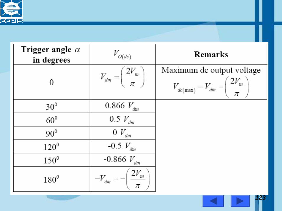
Control Characteristic of
Single Phase Half Wave Phase Controlled Rectifier
with Resistive Load

Power Electronics by Prof. M. Madhusudhan Rao 2121
( ) [ ]
The average dc output voltage is given by the expression
1 cos2
We can obtain the control characteristic by plotting the expression for the dc output voltage as a function of trigger angle
mO dc
VV απ
α
= +
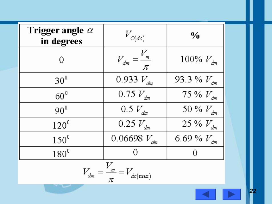
Power Electronics by Prof. M. Madhusudhan Rao 2222

Power Electronics by Prof. M. Madhusudhan Rao 2323
Control CharacteristicVO(dc)
Trigger angle in degreesα
0 60 120 180
Vdm
0.2 Vdm
0.6Vdm

Power Electronics by Prof. M. Madhusudhan Rao 2424
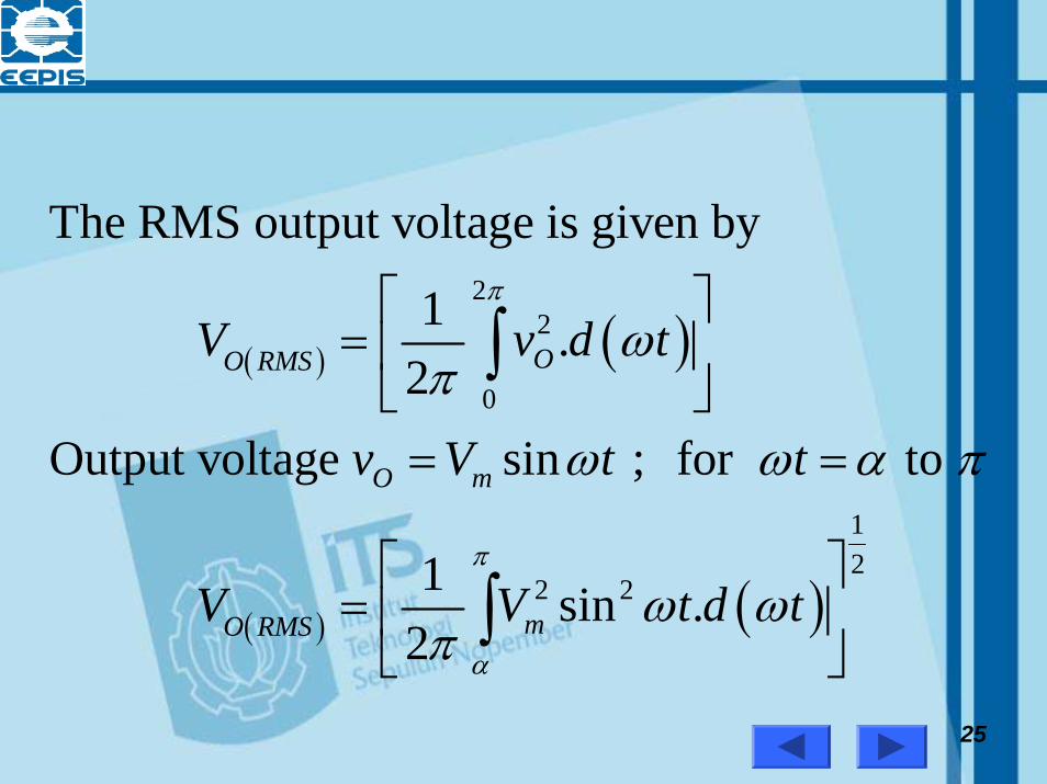
To Derive An Expression for the
RMS Value of Output Voltage of a
Single Phase Half Wave Controlled Rectifier With Resistive Load
Power Electronics by Prof. M. Madhusudhan Rao 2525
( ) ( )
( ) ( )
22
0
12
2 2
The RMS output voltage is given by
1 .2
Output voltage sin ; for to
1 sin .2
OO RMS
O m
mO RMS
V v d t
v V t t
V V t d t
π
π
α
ωπ
ω ω α π
ω ωπ
⎡ ⎤= ⎢ ⎥
⎣ ⎦= =
⎡ ⎤= ⎢ ⎥
⎣ ⎦
∫
∫

Power Electronics by Prof. M. Madhusudhan Rao 2626
( )( ) ( )
( ) ( ) ( )
( ) ( ) ( )
2
12
2
12 2
12 2
1 cos 2By substituting sin , we get2
1 cos 21 .2 2
1 cos 2 .4
cos 2 .4
mO RMS
mO RMS
mO RMS
tt
tV V d t
VV t d t
VV d t t d t
π
α
π
α
π π
α α
ωω
ωω
π
ω ωπ
ω ω ωπ
−=
⎡ ⎤−= ⎢ ⎥
⎣ ⎦
⎡ ⎤= −⎢ ⎥
⎣ ⎦
⎡ ⎤⎧ ⎫= −⎢ ⎥⎨ ⎬
⎢ ⎥⎩ ⎭⎣ ⎦
∫
∫
∫ ∫

Power Electronics by Prof. M. Madhusudhan Rao 2727
( ) ( )
( ) ( ) ( )
( ) ( )
( ) ( )
12
12
12
12
1 sin 222
sin 2 sin 21 ;sin2 02 2
1 sin 22 2
sin 222
mO RMS
mO RMS
mO RMS
mO RMS
V tV t
VV
VV
VV
π π
α α
ωωπ
π απ α π
π
απ απ
απ απ
⎡ ⎤⎧ ⎫⎛ ⎞= −⎢ ⎥⎨ ⎬⎜ ⎟⎝ ⎠⎢ ⎥⎩ ⎭⎣ ⎦
⎡ ⎤−⎛ ⎞= − − =⎢ ⎥⎜ ⎟
⎢ ⎥⎝ ⎠⎣ ⎦
⎡ ⎤⎛ ⎞= − +⎜ ⎟⎢ ⎥⎝ ⎠⎣ ⎦
⎛ ⎞= − +⎜ ⎟⎝ ⎠

Power Electronics by Prof. M. Madhusudhan Rao 2828
Performance Parameters Of
Phase Controlled Rectifiers

Power Electronics by Prof. M. Madhusudhan Rao 2929
( ) ( ) ( )
( )
( )
Output dc power (avg. or dc o/ppower delivered to the load)
; . .,
Whereavg./ dc value of o/p voltage.
avg./dc value of o/p current
dc dc dcO dc O dc O dc
dcO dc
dcO dc
P V I i e P V I
V V
I I
= × = ×
= =
= =

Power Electronics by Prof. M. Madhusudhan Rao 3030
( ) ( ) ( )
( )
( )
( )
( )
( )
Output ac power
Efficiency of Rectification (Rectification Ratio)
Efficiency ; % Efficiency 100
The o/p voltage consists of two componentsThe dc component
The ac
O ac O RMS O RMS
O dc O dc
O ac O ac
O dc
P V I
P P
P P
V
η η
= ×
= = ×
( )/ripple component ac r rmsV V=

Power Electronics by Prof. M. Madhusudhan Rao 3131
( ) ( ) ( )
( ) ( ) ( )
( )
( )
2 2
2 2
The total RMS value of output voltage is given by
Form Factor (FF) which is a measure of the shape of the output voltage is given by
RMS output l
O RMS O dc r rms
ac r rms O RMS O dc
O RMS
O dc
V V V
V V V V
VFF
V
= +
∴ = = −
= =( )
( )oad voltage
DC load output load voltage

Power Electronics by Prof. M. Madhusudhan Rao 3232
( )
( )
( ) ( )
( )
( )
( )
22 2
2
The Ripple Factor (RF) w.r.t. o/p voltage w/f
1
1
r rms acv
dcO dc
O RMS O dc O RMSv
O dc O dc
v
V Vr RFV V
V V Vr
V V
r FF
= = =
− ⎡ ⎤= = −⎢ ⎥
⎢ ⎥⎣ ⎦
∴ = −

Power Electronics by Prof. M. Madhusudhan Rao 3333
( )
( )
( ) ( ) ( )
( )
( ) ( ) ( )
( )
( ) ( ) ( )
2 2
max min
max min
Current Ripple Factor
Where
peak to peak ac ripple output voltage
peak to peak ac ripple load current
r rms aci
dcO dc
acr rms O RMS O dc
r pp
r pp O O
r pp
r pp O O
I IrI I
I I I I
V
V V V
I
I I I
= =
= = −
=
= −
=
= −

Power Electronics by Prof. M. Madhusudhan Rao 3434
( )
Transformer Utilization Factor (TUF)
Where RMS supply (secondary) voltageRMS supply (secondary) current
O dc
S S
S
S
PTUF
V I
VI
=×
==

Power Electronics by Prof. M. Madhusudhan Rao 3535

Power Electronics by Prof. M. Madhusudhan Rao 3636
1
Where Supply voltage at the transformer secondary side i/p supply current (transformer secondary winding current) Fundamental component of the i/p supply current Peak value of the input s
S
S
S
P
vi
iI
==
=
= upply currentPhase angle difference between (sine wave components) the fundamental components of i/p supply current & the input supply voltage.
φ =

Power Electronics by Prof. M. Madhusudhan Rao 3737
1
Displacement angle (phase angle)For an RL load
Displacement angle = Load impedance angle
tan for an RL load
Displacement Factor (DF) or Fundamental Power Factor
LR
DF Cos
φ
φωφ
φ
−
=
=
⎛ ⎞∴ = ⎜ ⎟⎝ ⎠
=

Power Electronics by Prof. M. Madhusudhan Rao 3838
11 2 22 2 21
21 1
1
Harmonic Factor (HF) orTotal Harmonic Distortion Factor ; THD
1
WhereRMS value of input supply current.RMS value of fundamental component of the i
S S S
S S
S
S
I I IHFI I
II
⎡ ⎤⎡ ⎤ ⎛ ⎞−⎢ ⎥= = −⎜ ⎟⎢ ⎥⎢ ⎥⎣ ⎦ ⎝ ⎠⎣ ⎦
==
/p supply current.

Power Electronics by Prof. M. Madhusudhan Rao 3939
( )
( )
1 1
Input Power Factor (PF)
cos cos
The Crest Factor (CF)
Peak input supply c
For an Ide
urrentRMS input supply current
1; 100% ; al Controlled Rectifier
0 ; 1;
S S S
S S S
S peak
S
ac r rms
V I IPFV I I
ICF
I
FF V V TUF
R
φ φ
η
= =
= =
= = = = =
0 ; 0; 1vF r HF THD PF DPF= = = = = =

Power Electronics by Prof. M. Madhusudhan Rao 4040
Single Phase Half Wave Controlled Rectifier
With An
RL Load

Power Electronics by Prof. M. Madhusudhan Rao 4141

Power Electronics by Prof. M. Madhusudhan Rao 4242
Input Supply Voltage (Vs)&
Thyristor (Output) Current Waveforms

Power Electronics by Prof. M. Madhusudhan Rao 4343

Power Electronics by Prof. M. Madhusudhan Rao 4444
Output (Load) Voltage Waveform

Power Electronics by Prof. M. Madhusudhan Rao 4545
To Derive An Expression For
Average (DC) Load Voltage of a Single Half Wave Controlled
Rectifier withRL Load

Power Electronics by Prof. M. Madhusudhan Rao 4646
( ) ( )
( ) ( ) ( ) ( )
( ) ( )
2
0
2
0
1 .2
1 . . .2
0 for 0 to & for to 2
1 . ;2
sin for to
L OO dc
L O O OO dc
O
L OO dc
O m
V V v d t
V V v d t v d t v d t
v t t
V V v d t
v V t t
π
βα π
α β
β
α
ωπ
ω ω ωπ
ω α ω β π
ωπ
ω ω α β
= =
⎡ ⎤= = + +⎢ ⎥
⎢ ⎥⎣ ⎦= = =
⎡ ⎤∴ = = ⎢ ⎥
⎣ ⎦= =
∫
∫ ∫ ∫
∫

Power Electronics by Prof. M. Madhusudhan Rao 4747
( ) ( )
( )
( ) ( )
( ) ( )
1 sin .2
cos2
cos cos2
cos cos2
L mO dc
mLO dc
mLO dc
mLO dc
V V V t d t
VV V t
VV V
VV V
β
α
β
α
ω ωπ
ωπ
α βπ
α βπ
⎡ ⎤= = ⎢ ⎥
⎣ ⎦⎡ ⎤
= = −⎢ ⎥⎣ ⎦
= = −
∴ = = −
∫

Power Electronics by Prof. M. Madhusudhan Rao 4848
During the period to the instantaneous o/p voltage is negative
reduces the average or the dc outputvo
and this
when compared to a purely resist
ltageive load.
tω π β=
Effect of Load Inductance on the Output

Power Electronics by Prof. M. Madhusudhan Rao 4949
Single Phase Half Wave Controlled Rectifier
With RL Load &
Free Wheeling Diode
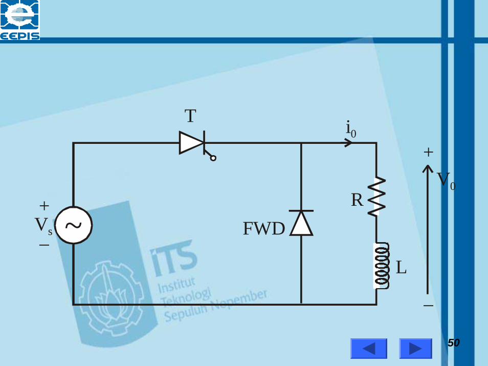
Power Electronics by Prof. M. Madhusudhan Rao 5050
V0
i0T
R
L
Vs ~+
+
−
−
FWD

Power Electronics by Prof. M. Madhusudhan Rao 5151
2π
2π
3π
3π
π
π
α
α
α
α
0
0
0
0
vS
iG
vO
ωt
ωt
ωt
ωt
Supply voltage
Load current
Load voltage
ωt=β
2π+α
Gate pulses
β
α
β
iO

Power Electronics by Prof. M. Madhusudhan Rao 5252
[ ]
The followi
The average
ng points a
output voltage
1 cos which is the same as that 2
of a purely resistive load.
For low value of inductance, the load current tends to become dis
re to be noted
cont
mdc
VV απ
= +
inuous.

Power Electronics by Prof. M. Madhusudhan Rao 5353
During the period to the load current is carried by the SCR.During the period to load current is carried by the free wheeling diode.The value of depends on the value of R and L and the forwa
α π
π β
βrd resistance
of the FWD.
Power Electronics by Prof. M. Madhusudhan Rao 5454
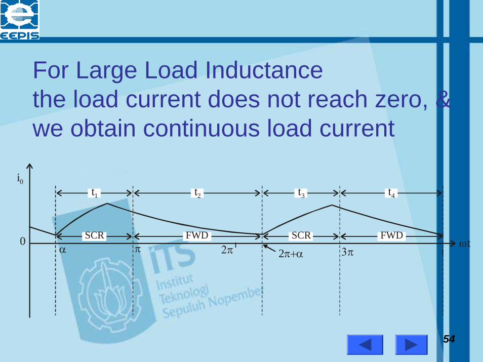
For Large Load Inductancethe load current does not reach zero, & we obtain continuous load current
2π 3ππα0 ωt
2π+α
t1
i0
SCR SCRFWD FWD
t3t2 t4

Power Electronics by Prof. M. Madhusudhan Rao 5555
Single Phase Half Wave Controlled Rectifier With
A General Load

Power Electronics by Prof. M. Madhusudhan Rao 5656
R
vS~+
− L
E+−
vO
iO

Power Electronics by Prof. M. Madhusudhan Rao 5757
1sin
For trigger angle ,the Thyristor conducts from to For trigger angle , the Thyristor conducts from to
m
EV
t
t
γ
α γω γ β
α γω α β
− ⎛ ⎞= ⎜ ⎟
⎝ ⎠<
=>
=
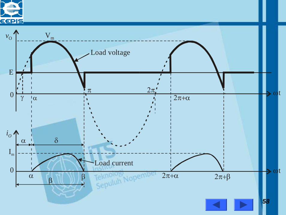
Power Electronics by Prof. M. Madhusudhan Rao 5858
0
0
iO
ωt
ωt
Load current
E
vO
Load voltage
γ απ 2π
2π+α
Vm
Im
α β 2π+α 2π+β
α
β
δ

Power Electronics by Prof. M. Madhusudhan Rao 5959
Equations
( )sin Input supply voltage.sin o/p load voltage for to .
for 0 to & for to 2 .
S m
O m
O
v V tv V t
tv E t
t
ωωω α βω αω β π
= =
= =
== =
=

Power Electronics by Prof. M. Madhusudhan Rao 6060
To Derive An
Expression For The Average Or
DC Load Voltage

Power Electronics by Prof. M. Madhusudhan Rao 6161
( ) ( )
( ) ( ) ( ) ( )
( ) ( ) ( )
2
0
2
0
2
0
sin Output load voltage
1 .2
1 .
for 0 to & for to 2for
. .
to
2
1 . sin .2
O
OO dc
O O OO d
m
m
c
O dc
O
V v d t
V v d t v d t v d t
V E d t V t E d t
v V tv E t t
t
π
βα π
α β
βα π
α β
ωπ
ω
ω ω α
ω ωπ
ω ω ωπ
ω α πβ
ω β
=
⎡ ⎤= + +⎢ ⎥
⎢ ⎥=
⎣ ⎦
⎡ ⎤= +
= == =
+⎢ ⎥
=
⎢ ⎥⎣ ⎦
∫
∫ ∫ ∫
∫ ∫ ∫

Power Electronics by Prof. M. Madhusudhan Rao 6262
( ) ( ) ( ) ( )
( ) ( ) ( ) ( )
( ) ( ) ( )
( ) ( ) ( )
2
0
1 cos2
1 0 cos cos 22
cos cos 22 2
2cos cos
2 2
mO dc
mO dc
mO dc
mO dc
V E t V t E t
V E V E
V EV
VV E
πα β
βα
ω ω ωπ
α β α π βπ
α β π β απ π
π β αα β
π π
⎡ ⎤= + − +⎢ ⎥
⎢ ⎥⎣ ⎦
= − − − + −⎡ ⎤⎣ ⎦
= − + − +⎡ ⎤ ⎡ ⎤⎣ ⎦ ⎣ ⎦
− −⎡ ⎤= − + ⎢ ⎥
⎣ ⎦

Power Electronics by Prof. M. Madhusudhan Rao 6363
( )
( ) ( )2
2
0
Conduction angle of thyristor
RMS Output Voltage can be calculated by using the expres
1 .
sion
2 OO RMSV v d tπ
ω
δ β α
π⎡ ⎤
= ⎥
=
⎢⎣
−
⎦∫

Power Electronics by Prof. M. Madhusudhan Rao 6464
Single Phase Full Wave Controlled Rectifier
Using A Center Tapped Transformer

Power Electronics by Prof. M. Madhusudhan Rao 6565
ACSupply
O
A
B
T1
T2
R L
vO
+

Power Electronics by Prof. M. Madhusudhan Rao 6666
Discontinuous Load Current Operation
without FWDfor
( )π β π α< < +

Power Electronics by Prof. M. Madhusudhan Rao 6767
vOVm
0α
2π 3πα π β( )π+α ( )π+β
αβ
iO
ωt
ωt0

Power Electronics by Prof. M. Madhusudhan Rao 6868
To Derive An Expression For The DC Output Voltage Of
A Single Phase Full Wave Controlled Rectifier With RL Load
(Without FWD)

Power Electronics by Prof. M. Madhusudhan Rao 6969
vOVm
0α
2π 3πα π β( )π+α ( )π+β
αβ
iO
ωt
ωt0

Power Electronics by Prof. M. Madhusudhan Rao 7070
( ) ( )
( ) ( )
( )
( ) ( )
1 .
1 sin .
cos
cos cos
dc OO dct
dc mO dc
mdcO dc
mdcO dc
V V v d t
V V V t d t
VV V t
VV V
β
ω α
β
α
β
α
ωπ
ω ωπ
ωπ
α βπ
=
= =
⎡ ⎤= = ⎢ ⎥
⎣ ⎦⎡ ⎤
= = −⎢ ⎥⎣ ⎦
= = −
∫
∫

Power Electronics by Prof. M. Madhusudhan Rao 7171
( )
( ) ( )
( ) ( )( )
( ) ( )
When the load inductance is negligible i.e., 0 Extinction angle radiansHence the average or dc output voltage for R load
cos cos
cos 1
1 cos ; for R load, when
mO dc
mO dc
mO dc
L
VV
VV
VV
β π
α ππ
απ
α β ππ
≈
=
= −
= − −
= + =

Power Electronics by Prof. M. Madhusudhan Rao 7272
( ) ( )2 2
To calculate the RMS output voltage we usethe expression
1 sin .mO RMSV V t d tβ
α
ω ωπ
⎡ ⎤= ⎢ ⎥
⎣ ⎦∫

Power Electronics by Prof. M. Madhusudhan Rao 7373
Discontinuous Load Current Operation with FWD

Power Electronics by Prof. M. Madhusudhan Rao 7474
vOVm
0α
2π 3πα π β( )π+α ( )π+β
αβ
iO
ωt
ωt0

Power Electronics by Prof. M. Madhusudhan Rao 7575
( )( )
2
2
1
1
Thyristor is trigger
Thyristor is triggered at ; conducts from to
FWD conducts from to &0 during discontinuous loa
ed at ;
conducts from t
d current.
o 2
O
T t
T
T t
t
T t
tv
ω π α
ω
ω αω
πω π β
α
α π
π
= +
==
≈
= +
=

Power Electronics by Prof. M. Madhusudhan Rao 7676
To Derive an Expression For The
DC Output Voltage ForA
Single Phase Full Wave Controlled Rectifier
With RL Load & FWD

Power Electronics by Prof. M. Madhusudhan Rao 7777
( ) ( )
( ) ( )
( )
( ) [ ]
( ) ( )
0
1 .
1 sin .
cos
cos cos ; cos 1
1 cos
dc OO dct
dc mO dc
mdcO dc
mdcO dc
mdcO dc
V V v d t
V V V t d t
VV V t
VV V
VV V
π
ω
π
α
π
α
ωπ
ω ωπ
ωπ
π α ππ
απ
=
= =
∴ = =
⎡ ⎤= = −⎢ ⎥
⎣ ⎦
= = − + = −
∴ = = +
∫
∫

Power Electronics by Prof. M. Madhusudhan Rao 7878
• The load current is discontinuous for low values of load inductance and for large values of trigger angles.
• For large values of load inductance the load current flows continuously without falling to zero.
• Generally the load current is continuous for large load inductance and for low trigger angles.

Power Electronics by Prof. M. Madhusudhan Rao 7979
Continuous Load Current Operation
(Without FWD)

Power Electronics by Prof. M. Madhusudhan Rao 8080
vOVm
0
2π 3πα π( )π+α
α
iO
ωt
ωt0
α α α
( )2π+α

Power Electronics by Prof. M. Madhusudhan Rao 8181
To Derive An Expression For
Average / DC Output VoltageOf
Single Phase Full Wave Controlled Rectifier For Continuous Current
Operation without FWD

Power Electronics by Prof. M. Madhusudhan Rao 8282
vOVm
0
2π 3πα π( )π+α
α
iO
ωt
ωt0
α α α
( )2π+α

Power Electronics by Prof. M. Madhusudhan Rao 8383
( ) ( )( )
( ) ( )( )
( )
( )
1 .
1 sin .
cos
dc OO dct
dc mO dc
mdcO dc
V V v d t
V V V t d t
VV V t
π α
ω α
π α
α
π α
α
ωπ
ω ωπ
ωπ
+
=
+
+
= =
⎡ ⎤= = ⎢ ⎥
⎢ ⎥⎣ ⎦⎡ ⎤
= = −⎢ ⎥⎣ ⎦
∫
∫

Power Electronics by Prof. M. Madhusudhan Rao 8484
( )
( )
( )
( ) [ ]
( )
cos cos ;
cos cos
cos cos
2 cos
dcO dc
m
mdcO dc
mdcO dc
V V
V
VV V
VV V
α π απ
π α α
α απ
απ
=
= − +⎡ ⎤⎣ ⎦
+ = −
= = +
∴ = =

Power Electronics by Prof. M. Madhusudhan Rao 8585
• By plotting VO(dc) versus α,we obtain the control characteristic of a single phase full wave controlled rectifier with RL load for continuous load current operation without FWD

Power Electronics by Prof. M. Madhusudhan Rao 8686
cosdc dmV V α= ×

Power Electronics by Prof. M. Madhusudhan Rao 8787
VO(dc)
Trigger angle in degreesα
030 60 90
Vdm
0.2 Vdm
0.6Vdm
-0.6 Vdm
-0.2Vdm
-Vdm
α
120 150 180
cosdc dmV V α= ×

Power Electronics by Prof. M. Madhusudhan Rao 8888
( )00
By varying the trigger angle we can vary the output dc voltage across the load. Hence we can control the dc output power flow to the load.
For trigger a . ., ngle , 0 to 90
cos is positive
0 90 ;
i e αα
α
≤ ≤
( )and hence is positive
Converter & are positive ; is positive
Controlled Rectif operates as a Power flow is from the
ie ac source to the d.
r.loa
dc dc dc dc d
d
c
cVV I P V I= ×

Power Electronics by Prof. M. Madhusudhan Rao 8989
( )
( )
0
0
0
0. ., 90 180 ,
is negative; is positive
For trigger angle , 90
; is negative.
Line
to 180
cos is negative and hence
In this case the conve Co
rtemmutated In
r operates s vea a
dc dc
dc dc dc
i e
V IP V I
α
α
α
≤ ≤
= ×
Power flows from the load ckt. to the i/p ac source.The inductive load energy is fed back to thei/p sou
rter.
rce.

Power Electronics by Prof. M. Madhusudhan Rao 9090
Drawbacks Of Full Wave Controlled Rectifier With Centre Tapped Transformer
• We require a centre tapped transformer which is quite heavier and bulky.
• Cost of the transformer is higher for the required dc output voltage & output power.
• Hence full wave bridge converters are preferred.
Power Electronics by Prof. M. Madhusudhan Rao 9191
Single Phase Full Wave Bridge Controlled Rectifier2 types of FW Bridge Controlled Rectifiers are
Half Controlled Bridge Converter (Semi-Converter)
Fully Controlled Bridge Converter (Full Converter)
The bridge full wave controlled rectifier does not require a centre tapped transformer

Power Electronics by Prof. M. Madhusudhan Rao 9292
Single Phase Full Wave Half Controlled Bridge
Converter (Single Phase Semi Converter)

Power Electronics by Prof. M. Madhusudhan Rao 9393
• Semi Converter with resistive load

Power Electronics by Prof. M. Madhusudhan Rao 9494
Input voltage, dc o/p voltage, dc o/p currentwaveform

Power Electronics by Prof. M. Madhusudhan Rao 9595
Power Electronics by Prof. M. Madhusudhan Rao 9696
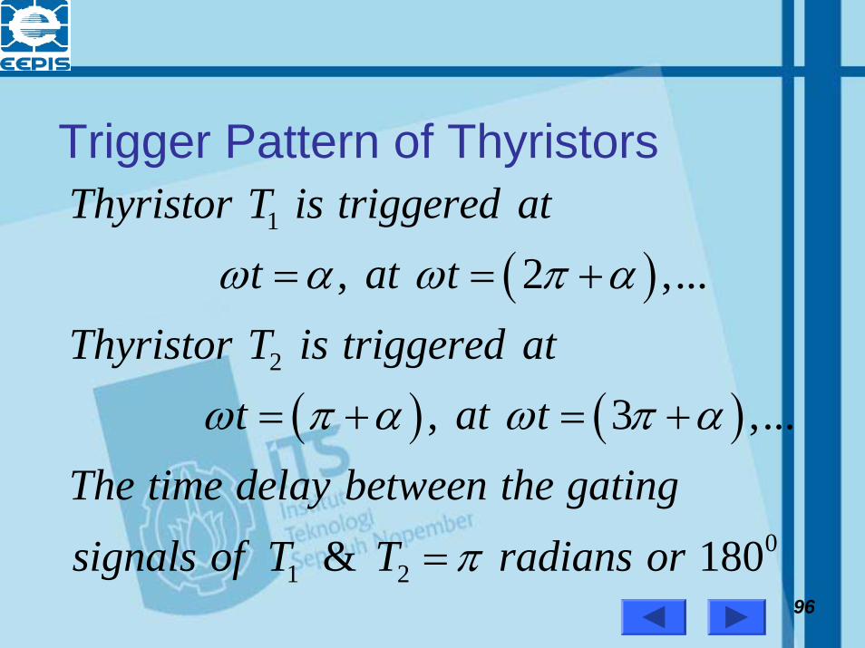
Trigger Pattern of Thyristors
( )
( ) ( )
1
2
01 2
, 2 ,...
, 3 ,...
& 180
Thyristor T is triggered att at t
Thyristor T is triggered att at t
The time delay between the gatingsignals of T T radians or
ω α ω π α
ω π α ω π α
π
= = +
= + = +
=

Power Electronics by Prof. M. Madhusudhan Rao 9797
Waveforms of single phase semi-converter
with general load & FWDfor α > 900

Power Electronics by Prof. M. Madhusudhan Rao 9898
Single Quadrant Operation

Power Electronics by Prof. M. Madhusudhan Rao 9999

Power Electronics by Prof. M. Madhusudhan Rao 100100

Power Electronics by Prof. M. Madhusudhan Rao 101101
( )
( )
1 1
2 2
Thyristor & conduct from
Thyristor & conduct from 2
FWD conducts during 0 to , ,...
T Dt to
T Dt to
t to
ω α π
ω π α π
ω α π π α
=
= +
= +
Power Electronics by Prof. M. Madhusudhan Rao 102102
Load Voltage & Load Current Waveform of Single Phase Semi
Converter forα < 900
& Continuous load current operation

Power Electronics by Prof. M. Madhusudhan Rao 103103
vOVm
0α
iO
ωt
2π 3πα π( )π+α
α
ωt0
α α
( )2π+α

Power Electronics by Prof. M. Madhusudhan Rao 104104
To Derive an Expression For The
DC Output Voltage ofA
Single Phase Semi-Converter With R,L, & E Load & FWD
For Continuous, Ripple Free Load Current Operation

Power Electronics by Prof. M. Madhusudhan Rao 105105
( ) ( )
( ) ( )
( )
( ) [ ]
( ) ( )
0
1 .
1 sin .
cos
cos cos ; cos 1
1 cos
dc OO dct
dc mO dc
mdcO dc
mdcO dc
mdcO dc
V V v d t
V V V t d t
VV V t
VV V
VV V
π
ω
π
α
π
α
ωπ
ω ωπ
ωπ
π α ππ
απ
=
= =
∴ = =
⎡ ⎤= = −⎢ ⎥
⎣ ⎦
= = − + = −
∴ = = +
∫
∫

Power Electronics by Prof. M. Madhusudhan Rao 106106
( )
( )
max
can be varied from a max. 2value of 0 by varying from 0 to .
For 0, The max. dc o/p voltage obtained is
Normalized dc o/p voltage is
2
11 cos
2
dc
m
m
dc
mdn
mdmdc
dcn n
VV to
VV
V V
VVV
V
V
π
α ππ
α
απ
π
= =
=
=
+=
⎛ ⎞⎜ ⎟⎝ ⎠
= = ( )1 cos2
α+

Power Electronics by Prof. M. Madhusudhan Rao 107107
RMS O/P Voltage VO(RMS)
( ) ( )
( ) ( ) ( )
( )
12
2 2
12 2
12
2 sin .2
1 cos 2 .2
1 sin 222
mO RMS
mO RMS
mO RMS
V V t d t
VV t d t
VV
π
α
π
α
ω ωπ
ω ωπ
απ απ
⎡ ⎤= ⎢ ⎥
⎣ ⎦
⎡ ⎤= −⎢ ⎥
⎣ ⎦
⎡ ⎤⎛ ⎞= − +⎜ ⎟⎢ ⎥⎝ ⎠⎣ ⎦
∫
∫

Power Electronics by Prof. M. Madhusudhan Rao 108108
Single Phase Full Wave Full Converter
(Fully Controlled Bridge Converter)
With R,L, & E Load

Power Electronics by Prof. M. Madhusudhan Rao 109109
Single phase full conveter with R load

Power Electronics by Prof. M. Madhusudhan Rao 110110
Input voltage, dc o/p voltage, dc o/p currentwaveform

Power Electronics by Prof. M. Madhusudhan Rao 111111

Power Electronics by Prof. M. Madhusudhan Rao 112112
Waveforms of Single Phase Full Converter
Assuming Continuous (Constant Load Current)
& Ripple Free Load Current

Power Electronics by Prof. M. Madhusudhan Rao 113113

Power Electronics by Prof. M. Madhusudhan Rao 114114

Power Electronics by Prof. M. Madhusudhan Rao 115115
iOConstant Load Current i =IO a
α π+α
α π+α 2π+α
ii
T1
T2&
Ia
π+α 2π+α 3π+α
ωt
ωt
ωtIai
iT3
T4&
Ia
Ia

Power Electronics by Prof. M. Madhusudhan Rao 116116
To Derive An Expression For
The Average DC Output Voltage of a Single Phase Full Converter
assuming Continuous & Constant Load Current

Power Electronics by Prof. M. Madhusudhan Rao 117117
( ) ( )2
0
The average dc output voltage can be determined by using the expression
1 . ;2
The o/p voltage waveform consists of two o/p pulses during the input supply time period of 0 to 2 r
dc OO dcV V v d tπ
ωπ
π
⎡ ⎤= = ⎢ ⎥
⎣ ⎦∫
adians. Hence the Average or dc o/p voltage can be calculated as

Power Electronics by Prof. M. Madhusudhan Rao 118118
( ) ( )
( ) [ ]
( )
2 sin .2
2 cos22 cos
dc mO dc
mdcO dc
mdcO dc
V V V t d t
VV V t
VV V
π α
α
π α
α
ω ωπ
ωπ
απ
+
+
⎡ ⎤= = ⎢ ⎥
⎣ ⎦
= = −
= =
∫

Power Electronics by Prof. M. Madhusudhan Rao 119119
( ) ( )
( )
0
max
max
Maximum average dc output voltage is calculated for a trigger angle 0and is obtained as
2 2cos 0
2
m mdmdc
mdmdc
V VV V
VV V
α
π π
π
=
= = × =
∴ = =

Power Electronics by Prof. M. Madhusudhan Rao 120120
( )
( )max
The normalized average output voltage is given by
2 coscos2
O dc dcdcn n
dmdc
m
dcn nm
V VV VV V
V
V V V
απ α
π
= = =
∴ = = =

Power Electronics by Prof. M. Madhusudhan Rao 121121
By plotting VO(dc) versus α,we obtain the control characteristic of a single phase full wave fully controlled
bridge converter (single phase full converter) for constant & continuous
load current operation.

Power Electronics by Prof. M. Madhusudhan Rao 122122
( )
To plot the control characteristic of a Single Phase Full Converter for constant& continuous load current operation.We use the equation for the average/ dc output voltage
2 cosmdcO dc
VV V απ
= =
Power Electronics by Prof. M. Madhusudhan Rao 123123

Power Electronics by Prof. M. Madhusudhan Rao 124124
VO(dc)
Trigger angle in degreesα
030 60 90
Vdm
0.2 Vdm
0.6Vdm
-0.6 Vdm
-0.2Vdm
-Vdm
α
120 150 180
cosdc dmV V α= ×

Power Electronics by Prof. M. Madhusudhan Rao 125125
• During the period from ωt = α to π the input voltage vS and the input current iS are both positive and the power flows from the supply to the load.
• The converter is said to be operated in the rectification mode
Controlled Rectifier Operationfor 0 < α < 900

Power Electronics by Prof. M. Madhusudhan Rao 126126
• During the period from ωt = π to (π+α), the input voltage vS is negative and the input current iS is positive and the output power becomes negative and there will be reverse power flow from the load circuit to the supply.
• The converter is said to be operated in the inversion mode.
Line Commutated Inverter Operationfor 900 < α < 1800

Power Electronics by Prof. M. Madhusudhan Rao 127127
Two Quadrant Operation of a Single Phase Full Converter
0<α < 900
Controlled Rectifier Operation
900<α <1800
Line CommutatedInverter Operation

Power Electronics by Prof. M. Madhusudhan Rao 128128
To Derive An Expression For The RMS Value Of The Output Voltage
( ) ( )2
2
0
The rms value of the output voltage is calculated as
1 .2 OO RMSV v d t
π
ωπ
⎡ ⎤= ⎢ ⎥
⎣ ⎦∫

Power Electronics by Prof. M. Madhusudhan Rao 129129
The single phase full converter gives two output voltage pulses during the input supply time period and hence the single phase full converter is referred to as a two pulse converter. The rms output vo
( ) ( )2
ltage can be calculated as
2 .2 OO RMSV v d t
π α
α
ωπ
+⎡ ⎤= ⎢ ⎥
⎣ ⎦∫

Power Electronics by Prof. M. Madhusudhan Rao 130130
( ) ( )
( ) ( )
( )( ) ( )
( ) ( ) ( )
2 2
22
2
2
1 sin .
sin .
1 cos 2.
2
cos 2 .2
mO RMS
mO RMS
mO RMS
mO RMS
V V t d t
VV t d t
tVV d t
VV d t t d t
π α
α
π α
α
π α
α
π α π α
α α
ω ωπ
ω ωπ
ωω
π
ω ω ωπ
+
+
+
+ +
⎡ ⎤= ⎢ ⎥
⎣ ⎦
⎡ ⎤= ⎢ ⎥
⎣ ⎦
⎡ ⎤−= ⎢ ⎥
⎣ ⎦
⎡ ⎤= −⎢ ⎥
⎣ ⎦
∫
∫
∫
∫ ∫

Power Electronics by Prof. M. Madhusudhan Rao 131131
( ) ( )
( ) ( ) ( )
( ) ( ) ( )
( )
2
2
2
sin 222
sin 2 sin 22 2
sin 2 2 sin 2;
2 2
sin 2 2 sin 2
mO RMS
mO RMS
mO RMS
V tV t
VV
VV
π α π α
α α
ωωπ
π α απ α α
π
π α απ
π
π α α
+ +⎡ ⎤⎛ ⎞= −⎢ ⎥⎜ ⎟⎝ ⎠⎣ ⎦
⎡ ⎤+ −⎛ ⎞= + − −⎢ ⎥⎜ ⎟
⎢ ⎥⎝ ⎠⎣ ⎦
⎡ ⎤+ −⎛ ⎞= −⎢ ⎥⎜ ⎟
⎢ ⎥⎝ ⎠⎣ ⎦+ =
Power Electronics by Prof. M. Madhusudhan Rao 132132
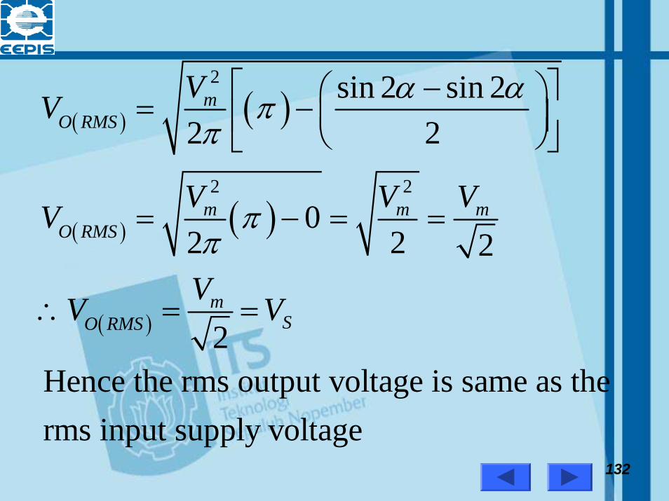
( ) ( )
( ) ( )
( )
2
2 2
sin 2 sin 22 2
02 2 2
2Hence the rms output voltage is same as the rms input supply voltage
mO RMS
m m mO RMS
mSO RMS
VV
V V VV
VV V
α αππ
ππ
⎡ − ⎤⎛ ⎞= − ⎜ ⎟⎢ ⎥⎝ ⎠⎣ ⎦
= − = =
∴ = =